EP3217431A1 - Semiconductor device capable of high-voltage operation - Google Patents
Semiconductor device capable of high-voltage operation Download PDFInfo
- Publication number
- EP3217431A1 EP3217431A1 EP17157038.5A EP17157038A EP3217431A1 EP 3217431 A1 EP3217431 A1 EP 3217431A1 EP 17157038 A EP17157038 A EP 17157038A EP 3217431 A1 EP3217431 A1 EP 3217431A1
- Authority
- EP
- European Patent Office
- Prior art keywords
- gate structure
- doped region
- semiconductor device
- top surface
- electrically coupled
- Prior art date
- Legal status (The legal status is an assumption and is not a legal conclusion. Google has not performed a legal analysis and makes no representation as to the accuracy of the status listed.)
- Granted
Links
Images




Classifications
-
- H—ELECTRICITY
- H10—SEMICONDUCTOR DEVICES; ELECTRIC SOLID-STATE DEVICES NOT OTHERWISE PROVIDED FOR
- H10D—INORGANIC ELECTRIC SEMICONDUCTOR DEVICES
- H10D30/00—Field-effect transistors [FET]
- H10D30/60—Insulated-gate field-effect transistors [IGFET]
-
- H—ELECTRICITY
- H10—SEMICONDUCTOR DEVICES; ELECTRIC SOLID-STATE DEVICES NOT OTHERWISE PROVIDED FOR
- H10D—INORGANIC ELECTRIC SEMICONDUCTOR DEVICES
- H10D64/00—Electrodes of devices having potential barriers
- H10D64/111—Field plates
- H10D64/112—Field plates comprising multiple field plate segments
-
- H—ELECTRICITY
- H10—SEMICONDUCTOR DEVICES; ELECTRIC SOLID-STATE DEVICES NOT OTHERWISE PROVIDED FOR
- H10D—INORGANIC ELECTRIC SEMICONDUCTOR DEVICES
- H10D30/00—Field-effect transistors [FET]
- H10D30/01—Manufacture or treatment
- H10D30/021—Manufacture or treatment of FETs having insulated gates [IGFET]
- H10D30/028—Manufacture or treatment of FETs having insulated gates [IGFET] of double-diffused metal oxide semiconductor [DMOS] FETs
- H10D30/0281—Manufacture or treatment of FETs having insulated gates [IGFET] of double-diffused metal oxide semiconductor [DMOS] FETs of lateral DMOS [LDMOS] FETs
-
- H—ELECTRICITY
- H10—SEMICONDUCTOR DEVICES; ELECTRIC SOLID-STATE DEVICES NOT OTHERWISE PROVIDED FOR
- H10D—INORGANIC ELECTRIC SEMICONDUCTOR DEVICES
- H10D30/00—Field-effect transistors [FET]
- H10D30/60—Insulated-gate field-effect transistors [IGFET]
- H10D30/64—Double-diffused metal-oxide semiconductor [DMOS] FETs
- H10D30/65—Lateral DMOS [LDMOS] FETs
-
- H—ELECTRICITY
- H10—SEMICONDUCTOR DEVICES; ELECTRIC SOLID-STATE DEVICES NOT OTHERWISE PROVIDED FOR
- H10D—INORGANIC ELECTRIC SEMICONDUCTOR DEVICES
- H10D62/00—Semiconductor bodies, or regions thereof, of devices having potential barriers
- H10D62/10—Shapes, relative sizes or dispositions of the regions of the semiconductor bodies; Shapes of the semiconductor bodies
- H10D62/102—Constructional design considerations for preventing surface leakage or controlling electric field concentration
- H10D62/103—Constructional design considerations for preventing surface leakage or controlling electric field concentration for increasing or controlling the breakdown voltage of reverse-biased devices
-
- H—ELECTRICITY
- H10—SEMICONDUCTOR DEVICES; ELECTRIC SOLID-STATE DEVICES NOT OTHERWISE PROVIDED FOR
- H10D—INORGANIC ELECTRIC SEMICONDUCTOR DEVICES
- H10D62/00—Semiconductor bodies, or regions thereof, of devices having potential barriers
- H10D62/10—Shapes, relative sizes or dispositions of the regions of the semiconductor bodies; Shapes of the semiconductor bodies
- H10D62/17—Semiconductor regions connected to electrodes not carrying current to be rectified, amplified or switched, e.g. channel regions
- H10D62/393—Body regions of DMOS transistors or IGBTs
-
- H—ELECTRICITY
- H10—SEMICONDUCTOR DEVICES; ELECTRIC SOLID-STATE DEVICES NOT OTHERWISE PROVIDED FOR
- H10D—INORGANIC ELECTRIC SEMICONDUCTOR DEVICES
- H10D64/00—Electrodes of devices having potential barriers
- H10D64/01—Manufacture or treatment
-
- H—ELECTRICITY
- H10—SEMICONDUCTOR DEVICES; ELECTRIC SOLID-STATE DEVICES NOT OTHERWISE PROVIDED FOR
- H10D—INORGANIC ELECTRIC SEMICONDUCTOR DEVICES
- H10D64/00—Electrodes of devices having potential barriers
- H10D64/111—Field plates
-
- H—ELECTRICITY
- H10—SEMICONDUCTOR DEVICES; ELECTRIC SOLID-STATE DEVICES NOT OTHERWISE PROVIDED FOR
- H10D—INORGANIC ELECTRIC SEMICONDUCTOR DEVICES
- H10D64/00—Electrodes of devices having potential barriers
- H10D64/20—Electrodes characterised by their shapes, relative sizes or dispositions
- H10D64/27—Electrodes not carrying the current to be rectified, amplified, oscillated or switched, e.g. gates
- H10D64/311—Gate electrodes for field-effect devices
- H10D64/411—Gate electrodes for field-effect devices for FETs
- H10D64/511—Gate electrodes for field-effect devices for FETs for IGFETs
-
- H—ELECTRICITY
- H10—SEMICONDUCTOR DEVICES; ELECTRIC SOLID-STATE DEVICES NOT OTHERWISE PROVIDED FOR
- H10D—INORGANIC ELECTRIC SEMICONDUCTOR DEVICES
- H10D30/00—Field-effect transistors [FET]
- H10D30/60—Insulated-gate field-effect transistors [IGFET]
- H10D30/611—Insulated-gate field-effect transistors [IGFET] having multiple independently-addressable gate electrodes influencing the same channel
-
- H—ELECTRICITY
- H10—SEMICONDUCTOR DEVICES; ELECTRIC SOLID-STATE DEVICES NOT OTHERWISE PROVIDED FOR
- H10D—INORGANIC ELECTRIC SEMICONDUCTOR DEVICES
- H10D62/00—Semiconductor bodies, or regions thereof, of devices having potential barriers
- H10D62/10—Shapes, relative sizes or dispositions of the regions of the semiconductor bodies; Shapes of the semiconductor bodies
- H10D62/17—Semiconductor regions connected to electrodes not carrying current to be rectified, amplified or switched, e.g. channel regions
- H10D62/351—Substrate regions of field-effect devices
- H10D62/357—Substrate regions of field-effect devices of FETs
- H10D62/364—Substrate regions of field-effect devices of FETs of IGFETs
- H10D62/371—Inactive supplementary semiconductor regions, e.g. for preventing punch-through, improving capacity effect or leakage current
Definitions
- the present invention relates to integrated circuits (ICs), and in particular to semiconductor devices capable of high-voltage operation.
- HV MOSFETs high-voltage metal-oxide-semiconductor field effect transistors
- HV MOSFETs high-voltage metal-oxide-semiconductor field effect transistors
- LDMOS lateral double diffused metal-oxide-semiconductor
- the semiconductor device includes a semiconductor substrate having a first conductivity type.
- a first well doped region is formed in a portion of the semiconductor substrate.
- the first well doped region has a second conductivity type that is the opposite of the first conductivity type.
- a first doped region is formed on the first well doped region, having the second conductivity type.
- a second doped region is formed on the first well doped region and is separated from the first doped region, having the second conductivity type.
- a first gate structure is formed over the first well doped region and is adjacent to the first doped region.
- a second gate structure is formed beside the first gate structure and is close to the second doped region.
- a third gate structure is formed overlapping a portion of the first gate structure and a first portion of the second gate structure.
- a semiconductor device includes a semiconductor substrate having a first conductivity type.
- a first well doped region is formed in a portion of the semiconductor substrate.
- the first well doped region has a second conductivity type that is the opposite of the first conductivity type.
- a first doped region is formed on the first well doped region, having the second conductivity type.
- a second doped region is formed on a portion of the first well doped region and separated from the first doped region, having the second conductivity type.
- a first gate structure is formed on the first well doped region and is close to the first doped region.
- a second gate structure is positioned close to the second doped region and is separated from the first gate structure.
- a third gate structure covers the first gate structure and the second gate structure.
- a first portion of a bottom surface of the third gate structure is in contact with a top surface of the first gate structure.
- a second portion of the bottom surface of the third gate structure is in contact with a top surface of the second gate structure.
- Yet another exemplary embodiment of a semiconductor device includes a semiconductor substrate having a first conductivity type.
- a first well doped region is formed in a portion of the semiconductor substrate, having a second conductivity type that is the opposite of the first conductivity type.
- a source doped region is formed on the first well doped region, having the second conductivity type.
- a drain doped region is formed on the first well doped region and is separated from the first doped region, having the second conductivity type.
- a gate structure is formed on the first well doped region and isclose to the source doped region.
- a first extended gate structure is formed covering and electrically coupled to the gate structure.
- a first dummy gate structure covers the first well doped region between the first extended gate structure and the drain doped region, so that the first extended gate structure is pulled away from the drain doped region by the dummy gate structure.
- Embodiments provide a semiconductor device.
- the semiconductor device may include a power metal-oxide-semiconductor (MOS) transistor.
- MOS metal-oxide-semiconductor
- the semiconductor device uses both a field plate gate structure and a dummy gate structure to extend a lateral distance between a source doped region and a drain doped region (i.e. a channel length) of the power MOS transistor.
- the lateral distance is along a direction that is substantially parallel to a top surface of a semiconductor substrate.
- the field plate gate structure overlaps a portion of a gate structure of the power MOS transistor and electrically connects to the gate structure of the power MOS.
- the field plate gate structure is composed of a resist-protection-oxide (RPO) pattern and a conductive layer pattern on the RPO pattern.
- RPO resist-protection-oxide
- the dummy poly gate structure is disposed laterally between the gate structure and the drain doped region and covered by the field plate gate structure.
- the dummy gate structure is used to prevent a silicide formed on the top surface of the semiconductor substrate between the field plate gate structure and the drain doped region.
- the dummy gate structure is electrically floating (i.e. electrically isolated form other components of the power MOS transistor). Therefore, the field plate gate, which is electrically coupled to the gate voltage, can be pulled away from the drain doped region, which is electrically coupled to a high operation voltage.
- the dummy poly gate structure and the gate structure may be formed simultaneously (in the same process). Alternatively, the dummy poly gate structure and the field plate gate structure may be formed simultaneously.
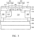
- FIGS. 1-6 are schematic cross-sectional views showing an intermediate stage of a method for forming a semiconductor device 500a in accordance with some embodiments of the disclosure.
- the semiconductor device 500a shown in FIG. 6 formed by the method shown in FIGS. 1-6 comprises a high-voltage metal-oxide-semiconductor field effect transistor (HV MOSFET) capable of high-voltage (e.g. 100 volts or above) operations.
- HV MOSFET high-voltage metal-oxide-semiconductor field effect transistor
- a semiconductor substrate 100 is provided.
- the semiconductor substrate 100 comprises a silicon substrate or a SiGe substrate.
- the semiconductor substrate 100 comprises a bulk semiconductor substrate, a strained semiconductor substrate or a compound semiconductor substrate.
- the semiconductor substrate 100 may have a first conductivity type such as P-type.
- An isolation element 108 is respectively disposed in opposite end portions of the semiconductor substrate 100 to define an active region for the semiconductor device 500a formed thereon.
- the isolation elements 108 can be the shallow trench isolation (STI) elements shown in FIG. 1 , but are not limited thereto.
- the isolation elements 108 can be field oxide (FOX) isolation elements.
- the isolation elements 108 may comprise insulating materials such as silicon oxides, but they are not limited thereto.
- a doped buried region 102 is formed in a portion of the semiconductor substrate 100 underlying the isolation elements 108.
- the doped buried region 102 may have a second conductive type that is the opposite of the first conductivity type, for example N-type.
- a well doped region 104 is formed between the doped buried region 102 and each of the isolation elements 108.
- a well doped region 106 is formed in a portion of the semiconductor substrate 100 between the well doped regions 104, and is above the doped buried region 102.
- the well doped regions 104 and the well doped region 106 may have the first conductivity type, for example P-type.
- a well doped region 110 is formed in the semiconductor substrate 100 between the isolation elements 108, the well doped region 106 and the well doped regions 104.
- a top surface 140 of the well doped region 110 is also located on the top surface of the semiconductor substrate 100.
- the well doped region 110 may have the second conductive type, for example N-type.
- a well doped region 112 is formed on a portion of the well doped region 110 and is adjacent to the one isolation element 108. Also, the well doped region 112 is surrounded by the well doped region 110 and the isolation element 108.
- the well doped region 112 may have the first conductivity type, for example P-type.
- a doped region 114 is formed in a portion of the well doped region 112, and may have the second conductivity type, for example N-type.
- Another doped region 116 is formed in a portion of the well doped region 110, and is adjacent to the right isolation element 108.
- the doped region 116 may have the second conductivity type, for example N-type.
- the doped region 114 and the doped region 116 may have a doping concentration greater than that of the well doped region 110.In some embodiments, the doped region 114 and the doped region 116 respectively serve as a source doped region and a drain doped region of the semiconductor device 500a.
- a gate structure G1 nd a gate structure G2 are formed on the well doped region 110, covering different portions of the well doped region 110.
- the gate structure G1 is formed over a portion of the well doped region 112 and a portion of the well doped region 110.
- the gate structure G1 is positioned adjacent to the doped region 114.
- the gate structure G2 formed over another portion of the well doped region 112, which is close to the drain doped region 116.
- the gate structure G2 is disposed adjacent to the drain doped region 116.
- the distance d1 between the doped region 114 and the doped region 116 i.e. the channel length of the semiconductor device 500a
- the gate structure G1 comprises a dielectric layer 118a and a conductive layer 120a formed over the dielectric layer 118a.
- the gate structure G2 comprises a dielectric layer 118b and a conductive layer 120b formed over the dielectric layer 118b.
- the gate dielectric layers 118a and 118b may comprise silicon oxide, silicon nitride or the like, and may have a thickness of about 23-140 A.
- the conductive layers 120a and 120b may comprise conductive materials such as polysilicon, metal or the like, and may have a thickness of about 800-2000 A.
- the gate dielectric layers 118a and 118b are formed simultaneously by a dielectric material deposition process and a subsequent patterning process.
- the conductive layers 120a and 120b are formed simultaneously by a conductive material deposition process and the subsequent patterning process. Therefore, a top surface of the gate structure G1 is coplanar with a top surface of the gate structure G2.
- a dielectric layer 122 is conformable and entirely formed on the well doped region 110.
- the dielectric layer 122 blanketly covers a top surface 140 of the well doped region 110 and the gate structures G1 and G2, as shown in FIG. 2 .
- the dielectric layer 122 is in contact with the gate structure G1 (including the gate dielectric layer 118a and the conductive layer 120a) and the gate structure G2 (including the gate dielectric layer 118b and the conductive layer 120b).
- the dielectric layer 122 may comprise silicon oxide, silicon nitride or the like, and may have a thickness of about 200-1200 A.
- the dielectric layer 122 may be thicker than the dielectric layers 118a and 118b.
- the dielectric layer 122 may serve as a resist-protection-oxide (RPO) layer.
- RPO resist-protection-oxide
- the RPO layer is used to cover a silicide-forbidden area of the active region, which avoids having the silicide formed thereon, during the silicidation process.
- a conductive layer 124 is conformably and entirely formed on the dielectric layer 122.
- the conductive layer 124 blanketly covers a top surface 141 of the dielectric layer 122, as shown in FIG. 3 .
- the conductive layer 124 may comprise conductive materials such as polysilicon, metal or the like, and may have a thickness of about 300-2000 ⁇ .
- the conductive layer 124 may be thicker than the conductive layers 120a and 120b.
- a patterned mask layer 126a as shown in FIG. 4 is formed over a portion of conductive layer 124 (see FIG. 3 ).
- the patterned mask layer 126a is formed by using a mask for patterning a resist-protection-oxide (RPO) layer.
- An etching process 128 is then performed to remove portions of the conductive layer 124 not covered by the patterned mask layer 126a.
- the patterned mask layer 126a may comprise materials such as photoresists or the like, and the etching process 128 can be, for example, a dry etching process.
- the etching process 128 stops on the dielectric layer 122, thereby forming a patterned conductive layer 124a.
- the patterned conductive layer 124a is formed overlapping a portion of the gate structure G1, a portion of the gate structure G2. Also, the patterned conductive layer 124a is formed covering a portion of the semiconductor substrate 100 between the gate structures G1 and G2.
- etching process 129 is performed to remove portions of the dielectric layer 122 (see FIG. 4 ) not covered by the patterned mask layer 126a and the patterned conductive layer 124a as shown in FIG. 5 .
- the etching process 129 can be, for example, a dry etching process. As shown in FIG. 5 , the etching process 129 stops on the conductive layer 120a and the semiconductor substrate 100, thereby respectively forming a patterned dielectric layer 122a.
- the patterned dielectric layer 122a is formed under the patterned conductive layer 124a. Also, the patterned dielectric layer 122a is formed over a portion of the gate structure G1, a portion of the gate structure G2 and a portion of the top surface 140 of the well doped region 110 between the gate structures G1 and G2.
- a gate structure G3 is formed overlapping the portion of the gate structure G1, the portion of the gate structure G2 and the portion of the well doped region 110 between the gate structures G1 and G2.
- the gate structure G3 serve as a field-plate gate structure of the semiconductor device 500a. After the aforementioned processes, the semiconductor device 500a is formed.
- a first portion 132a of a bottom surface 132 of the gate structure G3 is in contact with a top surface 134a of the gate structure G1.
- a second portion 132b of the bottom surface 132 of the gate structure G3 is in contact with a top surface 134b of the gate structure G2.
- the top surface 134a of the gate structure G1 is coplanar with the top surface 134b of the gate structure G2, as shown in FIG. 6 .
- the top surface 134a of the gate structure G1 and the top surface 134b of the gate structure G2 are not coplanar with a top surface 144a of the gate structure G3.
- the gate structure G3 comprises a first sidewall 136 and a second sidewall 138 opposite to the first sidewall 136.
- the first sidewall 136 is located directly on the gate structure G1
- the second sidewall 138 is located directly on the gate structure G2, as shown in FIG. 6 .
- the gate structure G3 includes the patterned conductive layer 124a and the patterned dielectric layer 122a, as shown in FIG. 6 . Therefore, a top surface 140 of the well doped region 110 between the doped region 114 and the doped region 116 (which also serves as the top surface of a channel region of the semiconductor device 500a) is entirely covered by the gate structure G1, the gate structure G2 and the gate structure G3. A patterned dielectric layer 122a of the gate structure G3 is in contact with the patterned conductive layer 118a of the gate structure G1 and the patterned conductive layer 118b of the gate structure G2.
- the gate structure G3 covers a portion of about 20 %-80 % of the top surface 134a of the underlying gate structure G1 comprising the conductive layer 120a and the dielectric layer 118a. Similarly, the gate structure G3 covers a portion of about 20 %-80 % of the top surface 134b of the underlying gate structure G2 comprising the conductive layer 120b and the dielectric layer 118b.
- conductive contacts 128a and 128b and a conductive line 130a can be further provided to the semiconductor device 500a.
- the conductive contact 128a is connected to the conductive layer 120a of the gate structure G1 and the conductive contact 128b is connected to the conductive layer 124a of the gate structure G3.
- the conductive contacts 128a and 128b are both connected the conductive line 130a, so that the gate structure G3 is electrically coupled to the gate structure G1.
- the gate structure G3 comprising the patterned conductive layer 124a and the patterned dielectric layer 122a and the gate structure G1 comprising the conductive layer 120a and the dielectric layer 118a may be provided with the same electrical potential during operations. Therefore, the gate structure G1 and the gate structure G3 may serve as a combined gate structure to increase the on-state current of the semiconductor device.
- the gate structure G3 is electrically coupled to the doped region 114 (i.e. the source doped region of the semiconductor device 500a) rather than to the gate structure G1. In other words, the gate structure G3 is electrically coupled to the reference potential VSS to increase the switching speed of the semiconductor device.
- the conductive contacts 128a and 128b may comprise conductive materials such as tungsten, copper or the like, and the conductive line 130a may comprise materials such as tungsten, copper or the like.
- the gate structure G2 is electrically floating. Therefore, the gate structure G2 may serve as a dummy gate structure. Also, the doped region 114, which serves as the source doped region of the semiconductor device 500a, is electrically coupled to a reference potential VSS. The doped region 116, which serves as the drain doped region of the semiconductor device 500a, is electrically coupled to a drain supply voltage VDD.
- the gate structure G3 may serve as a field plate gate structure.
- the gate structure G3, which comprises the patterned conductive layer 124a and the patterned dielectric layer 122a, and the gate structure G1, which comprises the conductive layer 120a and the dielectric layer 118a may be combined to function as a combined gate structure of the semiconductor device 500a capable of high-voltage operations. Therefore, the gate structure G3 may serve as an extended gate structure to reduce the surface electric field and to increase the on-state current of the semiconductor device 500a.
- the gate structure G3 is electrically coupled to the doped region 114 to increase the switching speed of the semiconductor device 500a.
- the doped region 114 and the doped region 116 may function as source doped region and drain doped region, respectively.
- the gate structure G3 is pulled away from the doped region 116 (the drain doped region) by the gate structure G2 to improve the breakdown voltage of the of the semiconductor device 500a. Also, the gate structure G2 is formed to prevent the undesired silicide from being formed on the channel region between the gate structure G1 and the doped region 116.
- FIG. 7 is a cross-sectional view of a semiconductor device 500b in accordance with some embodiments of the disclosure. Elements of the embodiments hereinafter that are the same or similar as those previously described with reference to FIGS. 1-6 , are not repeated for brevity.
- the semiconductor device 500a and the semiconductor device 500b are that the semiconductor device 500b further includes a gate structure G4 formed beside the gate structure G3 close to the doped region 116.
- the gate structure G4 also covers a portion 142b of the gate structure G2 and a portion of the top surface 140 of the well doped region 110 between the gate structure G2 and the doped region 116.
- the top surface 140 of the well doped region 110 between the doped region 114 and the doped region 116 (which also serves as the top surface of a channel region of the semiconductor device 500b) is entirely covered by the gate structure G1, the gate structure G2, the gate structure G3 and the gate structure G4.
- the gate structure G3, which is electrically coupled to the gate structure G1 is pulled away from the doped region 116 by the formation of the gate structure G2 and the gate structure G4.
- the gate structure G4 may be formed overlapping a portion of the doped region 116. Also, the gate structure G3 overlaps a first portion 142a of the gate structure G2. The gate structure G4 overlaps a second portion 142b of the gate structure G2, which is different from the first portion 142a.
- the gate structure G4 includes a patterned conductive layer 124b and a patterned dielectric layer 122b.
- the patterned dielectric layer 122b is formed by patterning the dielectric layer 122 through the etching process 128.
- the patterned conductive layer 124b is also formed by patterning the conductive layer 124 through the etching process 128.
- the patterned dielectric layers 122a and 122b are formed simultaneously.
- the patterned conductive layers 142a and 124b are formed simultaneously. Therefore, the gate structure G4 also serves as a field plate gate structure.
- a top surface 144a of the gate structure G3 is aligned to a top surface 144b of the gate structure G4.
- the gate structure G2 and gate structure G4 are electrically floating. Therefore, the gate structure G2 and gate structure G4 both serve as dummy gate structures.
- the gate structure G3 is electrically coupled to the gate structure G1 through the conductive contacts 128a and 128b and the conductive line 130a to increase the on-state current of the semiconductor device 500b.
- the gate structure G3 is electrically coupled to the doped region 114 through the conductive contact (not shown) to increase the switching speed of the semiconductor device 500b.
- the doped region 114 which serves as the source doped region of the semiconductor device 500b, is electrically coupled to the reference potential VSS.
- the doped region 116 which serves as the drain doped region of the semiconductor device 500b, is electrically coupled to the drain supply voltage VDD.
- the gate structure G3 is pulled away from the doped region 116 (the drain doped region) by the gate structure G2 and the gate structure G4, which serve as dummy gate structures, to improve the breakdown voltage of the of the semiconductor device 500b. Also, the gate structure G2 and the gate structure G4 are formed to prevent the undesired silicide from forming on the channel region between the gate structure G3 and the doped region 116.
- FIG. 8 is a cross-sectional view of a semiconductor device 500c in accordance with some embodiments of the disclosure. Elements of the embodiments hereinafter that are the same or similar as those previously described with reference to FIGS. 1-7 , are not repeated for brevity.
- the semiconductor device 500c further includes a gate structure G5 formed beside the gate structure G2 and adjacent to the doped region 116.
- the gate structure G5 is formed on the top surface 140 of the well doped region 110 between the gate structure G2 and the doped region 116.
- the gate structure G4 overlaps both the portion 142b of the gate structure G2 and a portion 146a of the gate structure G5.
- the top surface 140 of the well doped region 110 between the doped region 114 and the doped region 116 (which also serves as the top surface of a channel region of the semiconductor device 500c) is entirely covered by the gate structure G1, the gate structure G2, the gate structure G3, the gate structure G4 and the gate structure G5.
- the gate structure G4 covers the portion 142b of about 20 %-80 % of the top surface of the underlying gate structure G2 comprising the conductive layer 120b and the dielectric layer 118b. Similarly, the gate structure G4 covers the portion 146a of about 20 %-80 % of the top surface of the underlying gate structure G5 comprising the conductive layer 120c and the dielectric layer 118c.
- the gate structure G5 includes a dielectric layer 118c and a conductive layer 120c on the dielectric layer 118c.
- the dielectric layers 118a, 118b and 118c are formed simultaneously.
- the conductive layers 120a, 120b and 120c are formed simultaneously. Therefore, the top surface of gate structure G5 is coplanar with the top surface 134a of the gate structure G1 and the top surface 134b of the gate structure G2.
- the gate structure G4 may serve as a field plate gate structure.
- the gate structure G4 is electrically coupled to the gate structure G1 and the gate structure G3 through the conductive contacts 128a, 128b and 128c and the conductive line 130a.
- the gate structure G1, the gate structure G3 and the gate structure G4 may be collectively combined to function as a combined gate structure of the semiconductor device 500c capable of high-voltage operations. Therefore, the gate structure G3 and the gate structure G4 may serve as extended gate structures to increase the on-state current of the semiconductor device 500c.
- the gate structure G3 and he gate structure G4 are electrically coupled to the doped region 114 through the conductive contact (not shown) to increase the switching speed of the semiconductor device 500c.
- the gate structure G2 and gate structure G5 are electrically floating. Therefore, the gate structure G2 and gate structure G5 may serve as dummy gate structures. Also, the doped region 114, which serves as the source doped region of the semiconductor device 500c, is electrically coupled to the reference potential VSS. The doped region 116, which serves as the drain doped region of the semiconductor device 500c, is electrically coupled to the drain supply voltage VDD.
- the gate structure G4 is pulled away from the doped region 116 (the drain doped region) by the formation of the gate structure G5, which serve as dummy gate structures, to improve the breakdown voltage of the of the semiconductor device 500c. Also, the gate structure G5 is formed to prevent the undesired silicide from forming on the channel region between the gate structure G4 and the doped region 116.
- Embodiments provide semiconductor devices 500a-500c.
- the combined gate structure shown in FIGS. 6-8 Through the use of the combined gate structure shown in FIGS. 6-8 , a more uniform electric field contribution can be observed in the portion of the well doped region 110 underlying the combined gate structure during the operation of the semiconductor devices 500a-500c shown in FIGS. 6-8 when compared with another semiconductor device that is similar to the one shown in FIG. 6 , but which comprises only the gate structure G1 comprising a conductive layer 120a and a dielectric layer 118a and a dielectric layer 122. Also, the combined gate structure is pulled away from the drain doped region by the formation of the dummy gate structure to improve the breakdown voltage of the of the semiconductor device.
- the dummy gate structure is formed to prevent the undesired silicide from being formed on the channel region between the combined gate structure and the drain doped region of the semiconductor device. Accordingly, the semiconductor devices 500a-500c capable of high-voltage operation shown in FIGS. 6-8 can operate at a higher voltage of about 9-100 volts, which is about 100-1100 % higher than a semiconductor device that is similar to the one shown in FIG. 6 , but which comprises only the gate structure G1 comprising a conductive layer 120a and a dielectric layer 118a and a dielectric layer 122.
Landscapes
- Insulated Gate Type Field-Effect Transistor (AREA)
- Engineering & Computer Science (AREA)
- Manufacturing & Machinery (AREA)
- Metal-Oxide And Bipolar Metal-Oxide Semiconductor Integrated Circuits (AREA)
Abstract
Description
- This application claims the benefit of
U.S. Provisional Application No. 62/306,661 filed March 11,2016 U.S. Provisional Application No. 62/382,804 filed on September 2, 2016 - The present invention relates to integrated circuits (ICs), and in particular to semiconductor devices capable of high-voltage operation.
- Recently, as demand has increased for high-voltage devices such as power semiconductor devices, there has been an increasing interest in research on high-voltage metal-oxide-semiconductor field effect transistors (HV MOSFETs) applied in high-voltage devices.
- Among the various types of high-voltage metal-oxide-semiconductor field effect transistors (HV MOSFETs), semiconductor devices such as lateral double diffused metal-oxide-semiconductor (LDMOS) devices are often used.
- However, with progress being made in semiconductor fabrication, the breakdown voltage of high-voltage MOSFETs for high-voltage devices needs to be increased further. Thus, a reliable high-voltage MOSFET for high-voltage devices having an increased breakdown voltage is needed to meet device performance requirements as the needs in semiconductor fabrication of high-voltage devices continue.
- An exemplary embodiment of a semiconductor device is provided. The semiconductor device includes a semiconductor substrate having a first conductivity type. A first well doped region is formed in a portion of the semiconductor substrate. The first well doped region has a second conductivity type that is the opposite of the first conductivity type. A first doped region is formed on the first well doped region, having the second conductivity type. A second doped region is formed on the first well doped region and is separated from the first doped region, having the second conductivity type. A first gate structure is formed over the first well doped region and is adjacent to the first doped region. A second gate structure is formed beside the first gate structure and is close to the second doped region. A third gate structure is formed overlapping a portion of the first gate structure and a first portion of the second gate structure.
- Another exemplary embodiment of a semiconductor device includes a semiconductor substrate having a first conductivity type. A first well doped region is formed in a portion of the semiconductor substrate. The first well doped region has a second conductivity type that is the opposite of the first conductivity type. A first doped region is formed on the first well doped region, having the second conductivity type. A second doped region is formed on a portion of the first well doped region and separated from the first doped region, having the second conductivity type. A first gate structure is formed on the first well doped region and is close to the first doped region. A second gate structure is positioned close to the second doped region and is separated from the first gate structure. A third gate structure covers the first gate structure and the second gate structure. A first portion of a bottom surface of the third gate structure is in contact with a top surface of the first gate structure. A second portion of the bottom surface of the third gate structure is in contact with a top surface of the second gate structure.
- Yet another exemplary embodiment of a semiconductor device includes a semiconductor substrate having a first conductivity type. A first well doped region is formed in a portion of the semiconductor substrate, having a second conductivity type that is the opposite of the first conductivity type. A source doped region is formed on the first well doped region, having the second conductivity type. A drain doped region is formed on the first well doped region and is separated from the first doped region, having the second conductivity type. A gate structure is formed on the first well doped region and isclose to the source doped region. A first extended gate structure is formed covering and electrically coupled to the gate structure. A first dummy gate structure covers the first well doped region between the first extended gate structure and the drain doped region, so that the first extended gate structure is pulled away from the drain doped region by the dummy gate structure.
- A detailed description is given in the following embodiments with reference to the accompanying drawings.
- The invention can be more fully understood by reading the subsequent detailed description and examples with references made to the accompanying drawings, wherein:
-
FIGS. 1-6 are schematic cross-sectional views showing an intermediate stage of a method for forming a semiconductor device in accordance with some embodiments of the disclosure; -
FIG. 7 is a cross-sectional view of a semiconductor device in accordance with some embodiments of the disclosure; and -
FIG. 8 is a cross-sectional view of a semiconductor device in accordance with some embodiments of the disclosure. - The following description is of the best-contemplated mode of carrying out the invention. This description is made for the purpose of illustrating the general principles of the invention and should not be taken in a limiting sense. The scope of the invention is best determined by reference to the appended claims.
- Embodiments provide a semiconductor device. The semiconductor device may include a power metal-oxide-semiconductor (MOS) transistor. The semiconductor device uses both a field plate gate structure and a dummy gate structure to extend a lateral distance between a source doped region and a drain doped region (i.e. a channel length) of the power MOS transistor. The lateral distance is along a direction that is substantially parallel to a top surface of a semiconductor substrate. The field plate gate structure overlaps a portion of a gate structure of the power MOS transistor and electrically connects to the gate structure of the power MOS. The field plate gate structure is composed of a resist-protection-oxide (RPO) pattern and a conductive layer pattern on the RPO pattern. It should be noted that the dummy poly gate structure is disposed laterally between the gate structure and the drain doped region and covered by the field plate gate structure. The dummy gate structure is used to prevent a silicide formed on the top surface of the semiconductor substrate between the field plate gate structure and the drain doped region. Also, the dummy gate structure is electrically floating (i.e. electrically isolated form other components of the power MOS transistor). Therefore, the field plate gate, which is electrically coupled to the gate voltage, can be pulled away from the drain doped region, which is electrically coupled to a high operation voltage. A more uniform electric field contribution can be observed in a channel region (a region between a source doped region and the drain doped region) and a higher breakdown voltage (BVD) is obtained during operations of the of the power MOS transistor. In some embodiments, the dummy poly gate structure and the gate structure may be formed simultaneously (in the same process). Alternatively, the dummy poly gate structure and the field plate gate structure may be formed simultaneously.
-
FIGS. 1-6 are schematic cross-sectional views showing an intermediate stage of a method for forming asemiconductor device 500a in accordance with some embodiments of the disclosure. Thesemiconductor device 500a shown inFIG. 6 formed by the method shown inFIGS. 1-6 comprises a high-voltage metal-oxide-semiconductor field effect transistor (HV MOSFET) capable of high-voltage (e.g. 100 volts or above) operations. - In
FIG. 1 , asemiconductor substrate 100 is provided. As shown inFIG. 1 , thesemiconductor substrate 100 comprises a silicon substrate or a SiGe substrate. In some embodiments, thesemiconductor substrate 100 comprises a bulk semiconductor substrate, a strained semiconductor substrate or a compound semiconductor substrate. Thesemiconductor substrate 100 may have a first conductivity type such as P-type. Anisolation element 108 is respectively disposed in opposite end portions of thesemiconductor substrate 100 to define an active region for thesemiconductor device 500a formed thereon. Theisolation elements 108 can be the shallow trench isolation (STI) elements shown inFIG. 1 , but are not limited thereto. In some embodiments, theisolation elements 108 can be field oxide (FOX) isolation elements. Theisolation elements 108 may comprise insulating materials such as silicon oxides, but they are not limited thereto. - As shown in
FIG. 1 , a doped buriedregion 102 is formed in a portion of thesemiconductor substrate 100 underlying theisolation elements 108. The doped buriedregion 102 may have a second conductive type that is the opposite of the first conductivity type, for example N-type. Moreover, a welldoped region 104 is formed between the doped buriedregion 102 and each of theisolation elements 108. A well dopedregion 106 is formed in a portion of thesemiconductor substrate 100 between the welldoped regions 104, and is above the doped buriedregion 102. The welldoped regions 104 and the welldoped region 106 may have the first conductivity type, for example P-type. A well dopedregion 110 is formed in thesemiconductor substrate 100 between theisolation elements 108, the welldoped region 106 and the welldoped regions 104. Atop surface 140 of the welldoped region 110 is also located on the top surface of thesemiconductor substrate 100. The welldoped region 110 may have the second conductive type, for example N-type. A well dopedregion 112 is formed on a portion of the welldoped region 110 and is adjacent to the oneisolation element 108. Also, the welldoped region 112 is surrounded by the welldoped region 110 and theisolation element 108. The welldoped region 112 may have the first conductivity type, for example P-type. - As shown in
FIG. 1 , a dopedregion 114 is formed in a portion of the welldoped region 112, and may have the second conductivity type, for example N-type. Another dopedregion 116 is formed in a portion of the welldoped region 110, and is adjacent to theright isolation element 108. The dopedregion 116 may have the second conductivity type, for example N-type. The dopedregion 114 and the dopedregion 116 may have a doping concentration greater than that of the well doped region 110.In some embodiments, the dopedregion 114 and the dopedregion 116 respectively serve as a source doped region and a drain doped region of thesemiconductor device 500a. - A gate structure G1 nd a gate structure G2 are formed on the well
doped region 110, covering different portions of the welldoped region 110. The gate structure G1 is formed over a portion of the welldoped region 112 and a portion of the welldoped region 110. Also, the gate structure G1 is positioned adjacent to the dopedregion 114. The gate structure G2 formed over another portion of the welldoped region 112, which is close to the drain dopedregion 116. In this embodiment, the gate structure G2 is disposed adjacent to the drain dopedregion 116. As shown inFIG. 1 , the distance d1 between the dopedregion 114 and the doped region 116 (i.e. the channel length of thesemiconductor device 500a) is greater than the distance d2 between the gate structure G1 and the gate structure G2. - The gate structure G1 comprises a
dielectric layer 118a and aconductive layer 120a formed over thedielectric layer 118a. Similarly, the gate structure G2 comprises adielectric layer 118b and aconductive layer 120b formed over thedielectric layer 118b. In some embodiments, the gatedielectric layers conductive layers dielectric layers conductive layers - Next, a
dielectric layer 122 is conformable and entirely formed on the welldoped region 110. Thedielectric layer 122 blanketly covers atop surface 140 of the welldoped region 110 and the gate structures G1 and G2, as shown inFIG. 2 . Also, thedielectric layer 122 is in contact with the gate structure G1 (including thegate dielectric layer 118a and theconductive layer 120a) and the gate structure G2 (including thegate dielectric layer 118b and theconductive layer 120b). In some embodiments, thedielectric layer 122 may comprise silicon oxide, silicon nitride or the like, and may have a thickness of about 200-1200 A. Thedielectric layer 122 may be thicker than thedielectric layers dielectric layer 122 may serve as a resist-protection-oxide (RPO) layer. The RPO layer is used to cover a silicide-forbidden area of the active region, which avoids having the silicide formed thereon, during the silicidation process. - Next, a
conductive layer 124 is conformably and entirely formed on thedielectric layer 122. Theconductive layer 124 blanketly covers atop surface 141 of thedielectric layer 122, as shown inFIG. 3 . In some embodiments, theconductive layer 124 may comprise conductive materials such as polysilicon, metal or the like, and may have a thickness of about 300-2000 Å. Theconductive layer 124 may be thicker than theconductive layers - Next, a patterned
mask layer 126a as shown inFIG. 4 is formed over a portion of conductive layer 124 (seeFIG. 3 ). In some embodiments, the patternedmask layer 126a is formed by using a mask for patterning a resist-protection-oxide (RPO) layer. Anetching process 128 is then performed to remove portions of theconductive layer 124 not covered by the patternedmask layer 126a. As shown inFIG. 4 , the patternedmask layer 126a may comprise materials such as photoresists or the like, and theetching process 128 can be, for example, a dry etching process. Theetching process 128 stops on thedielectric layer 122, thereby forming a patternedconductive layer 124a. The patternedconductive layer 124a is formed overlapping a portion of the gate structure G1, a portion of the gate structure G2. Also, the patternedconductive layer 124a is formed covering a portion of thesemiconductor substrate 100 between the gate structures G1 and G2. - Next, another
etching process 129 is performed to remove portions of the dielectric layer 122 (seeFIG. 4 ) not covered by the patternedmask layer 126a and the patternedconductive layer 124a as shown inFIG. 5 . Theetching process 129 can be, for example, a dry etching process. As shown inFIG. 5 , theetching process 129 stops on theconductive layer 120a and thesemiconductor substrate 100, thereby respectively forming apatterned dielectric layer 122a. The patterneddielectric layer 122a is formed under the patternedconductive layer 124a. Also, the patterneddielectric layer 122a is formed over a portion of the gate structure G1, a portion of the gate structure G2 and a portion of thetop surface 140 of the welldoped region 110 between the gate structures G1 and G2. - In
FIG. 6 , after removal the patternedmask layer 126a (shown inFIG. 5 ), a gate structure G3 is formed overlapping the portion of the gate structure G1, the portion of the gate structure G2 and the portion of the welldoped region 110 between the gate structures G1 and G2. In some embodiments, the gate structure G3 serve as a field-plate gate structure of thesemiconductor device 500a. After the aforementioned processes, thesemiconductor device 500a is formed. - In some embodiments, a
first portion 132a of abottom surface 132 of the gate structure G3 is in contact with atop surface 134a of the gate structure G1. Asecond portion 132b of thebottom surface 132 of the gate structure G3 is in contact with atop surface 134b of the gate structure G2. Thetop surface 134a of the gate structure G1 is coplanar with thetop surface 134b of the gate structure G2, as shown inFIG. 6 . Also, thetop surface 134a of the gate structure G1 and thetop surface 134b of the gate structure G2 are not coplanar with atop surface 144a of the gate structure G3. - In some embodiments, the gate structure G3 comprises a
first sidewall 136 and asecond sidewall 138 opposite to thefirst sidewall 136. Thefirst sidewall 136 is located directly on the gate structure G1, and thesecond sidewall 138 is located directly on the gate structure G2, as shown inFIG. 6 . - In some embodiments, the gate structure G3 includes the patterned
conductive layer 124a and the patterneddielectric layer 122a, as shown inFIG. 6 . Therefore, atop surface 140 of the welldoped region 110 between the dopedregion 114 and the doped region 116 (which also serves as the top surface of a channel region of thesemiconductor device 500a) is entirely covered by the gate structure G1, the gate structure G2 and the gate structure G3. A patterneddielectric layer 122a of the gate structure G3 is in contact with the patternedconductive layer 118a of the gate structure G1 and the patternedconductive layer 118b of the gate structure G2. - In some embodiments, the gate structure G3 covers a portion of about 20 %-80 % of the
top surface 134a of the underlying gate structure G1 comprising theconductive layer 120a and thedielectric layer 118a. Similarly, the gate structure G3 covers a portion of about 20 %-80 % of thetop surface 134b of the underlying gate structure G2 comprising theconductive layer 120b and thedielectric layer 118b. - As shown in
FIG. 6 , for the ease of illustrating the electrical potential provided to thesemiconductor device 500a,conductive contacts conductive line 130a can be further provided to thesemiconductor device 500a. Theconductive contact 128a is connected to theconductive layer 120a of the gate structure G1 and theconductive contact 128b is connected to theconductive layer 124a of the gate structure G3. In some embodiments, theconductive contacts conductive line 130a, so that the gate structure G3 is electrically coupled to the gate structure G1. The gate structure G3 comprising the patternedconductive layer 124a and the patterneddielectric layer 122a and the gate structure G1 comprising theconductive layer 120a and thedielectric layer 118a may be provided with the same electrical potential during operations. Therefore, the gate structure G1 and the gate structure G3 may serve as a combined gate structure to increase the on-state current of the semiconductor device. - In some other embodiments, the gate structure G3 is electrically coupled to the doped region 114 (i.e. the source doped region of the
semiconductor device 500a) rather than to the gate structure G1. In other words, the gate structure G3 is electrically coupled to the reference potential VSS to increase the switching speed of the semiconductor device. - In some embodiments, the
conductive contacts conductive line 130a may comprise materials such as tungsten, copper or the like. - In some embodiments, the gate structure G2 is electrically floating. Therefore, the gate structure G2 may serve as a dummy gate structure. Also, the doped
region 114, which serves as the source doped region of thesemiconductor device 500a, is electrically coupled to a reference potential VSS. The dopedregion 116, which serves as the drain doped region of thesemiconductor device 500a, is electrically coupled to a drain supply voltage VDD. - As shown in
FIG. 6 , the gate structure G3 may serve as a field plate gate structure. In some embodiments, the gate structure G3, which comprises the patternedconductive layer 124a and the patterneddielectric layer 122a, and the gate structure G1, which comprises theconductive layer 120a and thedielectric layer 118a, may be combined to function as a combined gate structure of thesemiconductor device 500a capable of high-voltage operations. Therefore, the gate structure G3 may serve as an extended gate structure to reduce the surface electric field and to increase the on-state current of thesemiconductor device 500a. In some other embodiments, the gate structure G3 is electrically coupled to the dopedregion 114 to increase the switching speed of thesemiconductor device 500a. The dopedregion 114 and the dopedregion 116 may function as source doped region and drain doped region, respectively. - In this embodiment, the gate structure G3 is pulled away from the doped region 116 (the drain doped region) by the gate structure G2 to improve the breakdown voltage of the of the
semiconductor device 500a. Also, the gate structure G2 is formed to prevent the undesired silicide from being formed on the channel region between the gate structure G1 and the dopedregion 116. -
FIG. 7 is a cross-sectional view of asemiconductor device 500b in accordance with some embodiments of the disclosure. Elements of the embodiments hereinafter that are the same or similar as those previously described with reference toFIGS. 1-6 , are not repeated for brevity. One of the differences between thesemiconductor device 500a and thesemiconductor device 500b is that thesemiconductor device 500b further includes a gate structure G4 formed beside the gate structure G3 close to the dopedregion 116. The gate structure G4 also covers aportion 142b of the gate structure G2 and a portion of thetop surface 140 of the welldoped region 110 between the gate structure G2 and the dopedregion 116. Therefore, thetop surface 140 of the welldoped region 110 between the dopedregion 114 and the doped region 116 (which also serves as the top surface of a channel region of thesemiconductor device 500b) is entirely covered by the gate structure G1, the gate structure G2, the gate structure G3 and the gate structure G4. The gate structure G3, which is electrically coupled to the gate structure G1, is pulled away from the dopedregion 116 by the formation of the gate structure G2 and the gate structure G4. - In some other embodiments, the gate structure G4 may be formed overlapping a portion of the doped
region 116. Also, the gate structure G3 overlaps afirst portion 142a of the gate structure G2. The gate structure G4 overlaps asecond portion 142b of the gate structure G2, which is different from thefirst portion 142a. - As shown in
FIG. 7 , the gate structure G4 includes a patternedconductive layer 124b and a patterneddielectric layer 122b. The patterneddielectric layer 122b is formed by patterning thedielectric layer 122 through theetching process 128. Similarly, the patternedconductive layer 124b is also formed by patterning theconductive layer 124 through theetching process 128. In other words, the patterneddielectric layers conductive layers top surface 144a of the gate structure G3 is aligned to atop surface 144b of the gate structure G4. - In some embodiments, the gate structure G2 and gate structure G4 are electrically floating. Therefore, the gate structure G2 and gate structure G4 both serve as dummy gate structures. In some embodiments, the gate structure G3 is electrically coupled to the gate structure G1 through the
conductive contacts conductive line 130a to increase the on-state current of thesemiconductor device 500b. In some other embodiments, the gate structure G3 is electrically coupled to the dopedregion 114 through the conductive contact (not shown) to increase the switching speed of thesemiconductor device 500b. Also, the dopedregion 114, which serves as the source doped region of thesemiconductor device 500b, is electrically coupled to the reference potential VSS. The dopedregion 116, which serves as the drain doped region of thesemiconductor device 500b, is electrically coupled to the drain supply voltage VDD. - In this embodiment, the gate structure G3 is pulled away from the doped region 116 (the drain doped region) by the gate structure G2 and the gate structure G4, which serve as dummy gate structures, to improve the breakdown voltage of the of the
semiconductor device 500b. Also, the gate structure G2 and the gate structure G4 are formed to prevent the undesired silicide from forming on the channel region between the gate structure G3 and the dopedregion 116. -
FIG. 8 is a cross-sectional view of asemiconductor device 500c in accordance with some embodiments of the disclosure. Elements of the embodiments hereinafter that are the same or similar as those previously described with reference toFIGS. 1-7 , are not repeated for brevity. One of the differences between thesemiconductor device 500c and thesemiconductor device 500b (FIG. 7 ) is that thesemiconductor device 500c further includes a gate structure G5 formed beside the gate structure G2 and adjacent to the dopedregion 116. The gate structure G5 is formed on thetop surface 140 of the welldoped region 110 between the gate structure G2 and the dopedregion 116. The gate structure G4 overlaps both theportion 142b of the gate structure G2 and aportion 146a of the gate structure G5. Therefore, thetop surface 140 of the welldoped region 110 between the dopedregion 114 and the doped region 116 (which also serves as the top surface of a channel region of thesemiconductor device 500c) is entirely covered by the gate structure G1, the gate structure G2, the gate structure G3, the gate structure G4 and the gate structure G5. - In some embodiments, the gate structure G4 covers the
portion 142b of about 20 %-80 % of the top surface of the underlying gate structure G2 comprising theconductive layer 120b and thedielectric layer 118b. Similarly, the gate structure G4 covers theportion 146a of about 20 %-80 % of the top surface of the underlying gate structure G5 comprising theconductive layer 120c and thedielectric layer 118c. - As shown in
FIG. 8 , the gate structure G5 includes adielectric layer 118c and aconductive layer 120c on thedielectric layer 118c. Thedielectric layers conductive layers top surface 134a of the gate structure G1 and thetop surface 134b of the gate structure G2. - As shown in
FIG. 8 , the gate structure G4 may serve as a field plate gate structure. In some embodiments, the gate structure G4 is electrically coupled to the gate structure G1 and the gate structure G3 through theconductive contacts conductive line 130a. The gate structure G1, the gate structure G3 and the gate structure G4 may be collectively combined to function as a combined gate structure of thesemiconductor device 500c capable of high-voltage operations. Therefore, the gate structure G3 and the gate structure G4 may serve as extended gate structures to increase the on-state current of thesemiconductor device 500c. In some other embodiments, the gate structure G3 and he gate structure G4 are electrically coupled to the dopedregion 114 through the conductive contact (not shown) to increase the switching speed of thesemiconductor device 500c. - In some embodiments, the gate structure G2 and gate structure G5 are electrically floating. Therefore, the gate structure G2 and gate structure G5 may serve as dummy gate structures. Also, the doped
region 114, which serves as the source doped region of thesemiconductor device 500c, is electrically coupled to the reference potential VSS. The dopedregion 116, which serves as the drain doped region of thesemiconductor device 500c, is electrically coupled to the drain supply voltage VDD. - In this embodiment, the gate structure G4 is pulled away from the doped region 116 (the drain doped region) by the formation of the gate structure G5, which serve as dummy gate structures, to improve the breakdown voltage of the of the
semiconductor device 500c. Also, the gate structure G5 is formed to prevent the undesired silicide from forming on the channel region between the gate structure G4 and the dopedregion 116. - Embodiments provide
semiconductor devices 500a-500c. Through the use of the combined gate structure shown inFIGS. 6-8 , a more uniform electric field contribution can be observed in the portion of the welldoped region 110 underlying the combined gate structure during the operation of thesemiconductor devices 500a-500c shown inFIGS. 6-8 when compared with another semiconductor device that is similar to the one shown inFIG. 6 , but which comprises only the gate structure G1 comprising aconductive layer 120a and adielectric layer 118a and adielectric layer 122. Also, the combined gate structure is pulled away from the drain doped region by the formation of the dummy gate structure to improve the breakdown voltage of the of the semiconductor device. The dummy gate structure is formed to prevent the undesired silicide from being formed on the channel region between the combined gate structure and the drain doped region of the semiconductor device. Accordingly, thesemiconductor devices 500a-500c capable of high-voltage operation shown inFIGS. 6-8 can operate at a higher voltage of about 9-100 volts, which is about 100-1100 % higher than a semiconductor device that is similar to the one shown inFIG. 6 , but which comprises only the gate structure G1 comprising aconductive layer 120a and adielectric layer 118a and adielectric layer 122. - While the invention has been described by way of example and in terms of the preferred embodiments, it is to be understood that the invention is not limited to the disclosed embodiments. On the contrary, it is intended to cover various modifications and similar arrangements (as would be apparent to those skilled in the art). Therefore, the scope of the appended claims should be accorded the broadest interpretation so as to encompass all such modifications and similar arrangements.
Claims (14)
Applications Claiming Priority (3)
| Application Number | Priority Date | Filing Date | Title |
|---|---|---|---|
| US201662306661P | 2016-03-11 | 2016-03-11 | |
| US201662382804P | 2016-09-02 | 2016-09-02 | |
| US15/425,207 US10396166B2 (en) | 2016-03-11 | 2017-02-06 | Semiconductor device capable of high-voltage operation |
Publications (2)
| Publication Number | Publication Date |
|---|---|
| EP3217431A1 true EP3217431A1 (en) | 2017-09-13 |
| EP3217431B1 EP3217431B1 (en) | 2022-04-20 |
Family
ID=58098537
Family Applications (1)
| Application Number | Title | Priority Date | Filing Date |
|---|---|---|---|
| EP17157038.5A Active EP3217431B1 (en) | 2016-03-11 | 2017-02-21 | Semiconductor device capable of high-voltage operation |
Country Status (4)
| Country | Link |
|---|---|
| US (1) | US10396166B2 (en) |
| EP (1) | EP3217431B1 (en) |
| CN (1) | CN107180870B (en) |
| TW (1) | TWI637520B (en) |
Families Citing this family (11)
| Publication number | Priority date | Publication date | Assignee | Title |
|---|---|---|---|---|
| US10396166B2 (en) | 2016-03-11 | 2019-08-27 | Mediatek Inc. | Semiconductor device capable of high-voltage operation |
| US10418480B2 (en) | 2016-03-11 | 2019-09-17 | Mediatek Inc. | Semiconductor device capable of high-voltage operation |
| US10199496B2 (en) | 2016-03-11 | 2019-02-05 | Mediatek Inc. | Semiconductor device capable of high-voltage operation |
| CN108630754B (en) * | 2017-03-24 | 2021-04-27 | 立锜科技股份有限公司 | High voltage components |
| CN108682689B (en) * | 2018-05-25 | 2023-12-01 | 矽力杰半导体技术(杭州)有限公司 | Laterally diffused metal oxide semiconductor structure and method of forming same |
| TWI699888B (en) * | 2018-11-07 | 2020-07-21 | 新唐科技股份有限公司 | High voltage semiconductor devices |
| CN111508843B (en) * | 2019-01-31 | 2023-07-14 | 中芯国际集成电路制造(上海)有限公司 | Semiconductor device and method of forming the same |
| KR102220445B1 (en) * | 2019-07-01 | 2021-02-25 | 삼성전자주식회사 | Semiconductor device and manufacturing method having the same |
| US11355596B2 (en) * | 2019-12-17 | 2022-06-07 | Taiwan Semiconductor Manufacturing Company, Ltd. | High power device with self-aligned field plate |
| CN114975574A (en) * | 2021-02-19 | 2022-08-30 | 联华电子股份有限公司 | High Voltage Semiconductor Devices |
| CN117133801A (en) * | 2022-05-20 | 2023-11-28 | 联华电子股份有限公司 | Gallium nitride element with field plate structure and manufacturing method thereof |
Citations (5)
| Publication number | Priority date | Publication date | Assignee | Title |
|---|---|---|---|---|
| US6710416B1 (en) * | 2003-05-16 | 2004-03-23 | Agere Systems Inc. | Split-gate metal-oxide-semiconductor device |
| US20080070371A1 (en) * | 2006-09-18 | 2008-03-20 | Promos Technologies Inc. | Semiconductor Device and Manufacturing Method Thereof |
| US20120126323A1 (en) * | 2010-11-23 | 2012-05-24 | Macronix International Co., Ltd. | Semiconductor device having a split gate and a super-junction structure |
| WO2012147456A1 (en) * | 2011-04-26 | 2012-11-01 | シャープ株式会社 | Semiconductor device |
| US20160172490A1 (en) * | 2014-12-16 | 2016-06-16 | Vanguard International Semiconductor Corporation | High- voltage semiconductor device and method for manufacturing the same |
Family Cites Families (32)
| Publication number | Priority date | Publication date | Assignee | Title |
|---|---|---|---|---|
| US4811078A (en) | 1985-05-01 | 1989-03-07 | Texas Instruments Incorporated | Integrated circuit device and process with tin capacitors |
| US5393691A (en) | 1993-07-28 | 1995-02-28 | Taiwan Semiconductor Manufacturing Company | Fabrication of w-polycide-to-poly capacitors with high linearity |
| JPH09237841A (en) | 1996-02-29 | 1997-09-09 | Toshiba Corp | Semiconductor device and manufacturing method thereof |
| KR100302611B1 (en) | 1999-06-07 | 2001-10-29 | 김영환 | High power semiconductor device and fabrication method thereof |
| SG165138A1 (en) * | 2000-07-12 | 2010-10-28 | Inst Of Microelectronics | A semiconductor device |
| US6461902B1 (en) * | 2000-07-18 | 2002-10-08 | Institute Of Microelectronics | RF LDMOS on partial SOI substrate |
| US7253486B2 (en) | 2002-07-31 | 2007-08-07 | Freescale Semiconductor, Inc. | Field plate transistor with reduced field plate resistance |
| US6825531B1 (en) | 2003-07-11 | 2004-11-30 | Micrel, Incorporated | Lateral DMOS transistor with a self-aligned drain region |
| EP1661186A2 (en) * | 2003-08-27 | 2006-05-31 | Koninklijke Philips Electronics N.V. | Electronic device comprising an ldmos transistor |
| US7573078B2 (en) | 2004-05-11 | 2009-08-11 | Cree, Inc. | Wide bandgap transistors with multiple field plates |
| US9773877B2 (en) | 2004-05-13 | 2017-09-26 | Cree, Inc. | Wide bandgap field effect transistors with source connected field plates |
| KR100731054B1 (en) | 2005-10-28 | 2007-06-22 | 동부일렉트로닉스 주식회사 | Power semiconductor device and manufacturing method thereof |
| US7824968B2 (en) | 2006-07-17 | 2010-11-02 | Chartered Semiconductor Manufacturing Ltd | LDMOS using a combination of enhanced dielectric stress layer and dummy gates |
| US8247869B2 (en) * | 2010-04-26 | 2012-08-21 | Freescale Semiconductor, Inc. | LDMOS transistors with a split gate |
| US8860120B2 (en) | 2010-09-22 | 2014-10-14 | Nxp, B.V. | Field modulating plate and circuit |
| CN102569079B (en) | 2010-12-17 | 2014-12-10 | 上海华虹宏力半导体制造有限公司 | Preparation method of dual-grid LDMOS (laterally diffused metal oxide semiconductor) with self-aligned metal silicification technology |
| US8610206B2 (en) * | 2011-02-18 | 2013-12-17 | Macronix International Co., Ltd. | Split-gate lateral diffused metal oxide semiconductor device |
| US20130020632A1 (en) | 2011-07-18 | 2013-01-24 | Disney Donald R | Lateral transistor with capacitively depleted drift region |
| US8680615B2 (en) * | 2011-12-13 | 2014-03-25 | Freescale Semiconductor, Inc. | Customized shield plate for a field effect transistor |
| US9087920B2 (en) * | 2012-06-01 | 2015-07-21 | Taiwan Semiconductor Manufacturing Company, Ltd. | Vertical power MOSFET and methods of forming the same |
| JP6009341B2 (en) * | 2012-12-13 | 2016-10-19 | ルネサスエレクトロニクス株式会社 | Semiconductor device |
| US9859399B2 (en) * | 2013-11-05 | 2018-01-02 | Vanguard International Semiconductor Corporation | Lateral diffused semiconductor device with ring field plate |
| KR102154336B1 (en) | 2014-01-09 | 2020-09-10 | 한국전자통신연구원 | Field-Effect Transistors for High Voltage Operation and Manufacturing Method Thereof |
| US9490360B2 (en) | 2014-02-19 | 2016-11-08 | United Microelectronics Corp. | Semiconductor device and operating method thereof |
| US9373712B2 (en) * | 2014-09-29 | 2016-06-21 | Taiwan Semiconductor Manufacturing Co., Ltd. | Transistor and method of manufacturing the same |
| US9627528B2 (en) * | 2015-09-11 | 2017-04-18 | Macronix International Co., Ltd. | Semiconductor device having gate structures and manufacturing method thereof |
| CN106531794B (en) * | 2015-09-15 | 2021-02-09 | 联华电子股份有限公司 | High voltage metal oxide semiconductor transistor element and manufacturing method thereof |
| TWI672815B (en) * | 2015-10-14 | 2019-09-21 | United Microelectronics Corp. | Metal-oxide-semiconductor transistor and method of forming gate layout |
| US10205024B2 (en) * | 2016-02-05 | 2019-02-12 | Taiwan Semiconductor Manufacturing Company Ltd. | Semiconductor structure having field plate and associated fabricating method |
| US10396166B2 (en) | 2016-03-11 | 2019-08-27 | Mediatek Inc. | Semiconductor device capable of high-voltage operation |
| US10418480B2 (en) | 2016-03-11 | 2019-09-17 | Mediatek Inc. | Semiconductor device capable of high-voltage operation |
| US10199496B2 (en) | 2016-03-11 | 2019-02-05 | Mediatek Inc. | Semiconductor device capable of high-voltage operation |
-
2017
- 2017-02-06 US US15/425,207 patent/US10396166B2/en active Active
- 2017-02-21 EP EP17157038.5A patent/EP3217431B1/en active Active
- 2017-02-24 CN CN201710103833.4A patent/CN107180870B/en active Active
- 2017-03-08 TW TW106107513A patent/TWI637520B/en not_active IP Right Cessation
Patent Citations (5)
| Publication number | Priority date | Publication date | Assignee | Title |
|---|---|---|---|---|
| US6710416B1 (en) * | 2003-05-16 | 2004-03-23 | Agere Systems Inc. | Split-gate metal-oxide-semiconductor device |
| US20080070371A1 (en) * | 2006-09-18 | 2008-03-20 | Promos Technologies Inc. | Semiconductor Device and Manufacturing Method Thereof |
| US20120126323A1 (en) * | 2010-11-23 | 2012-05-24 | Macronix International Co., Ltd. | Semiconductor device having a split gate and a super-junction structure |
| WO2012147456A1 (en) * | 2011-04-26 | 2012-11-01 | シャープ株式会社 | Semiconductor device |
| US20160172490A1 (en) * | 2014-12-16 | 2016-06-16 | Vanguard International Semiconductor Corporation | High- voltage semiconductor device and method for manufacturing the same |
Also Published As
| Publication number | Publication date |
|---|---|
| CN107180870A (en) | 2017-09-19 |
| US20170263717A1 (en) | 2017-09-14 |
| US10396166B2 (en) | 2019-08-27 |
| CN107180870B (en) | 2020-03-10 |
| TW201733125A (en) | 2017-09-16 |
| EP3217431B1 (en) | 2022-04-20 |
| TWI637520B (en) | 2018-10-01 |
Similar Documents
| Publication | Publication Date | Title |
|---|---|---|
| EP3217432B1 (en) | Semiconductor device capable of high-voltage operation | |
| EP3217431B1 (en) | Semiconductor device capable of high-voltage operation | |
| US10170589B2 (en) | Vertical power MOSFET and methods for forming the same | |
| US8803234B1 (en) | High voltage semiconductor device and method for fabricating the same | |
| US10134868B2 (en) | MOS devices with mask layers and methods for forming the same | |
| US10879389B2 (en) | Semiconductor device capable of high-voltage operation | |
| CN105118855A (en) | Semiconductor elements with gate dielectrics of various thicknesses | |
| US11145718B2 (en) | Semiconductor device with separate active region and method of fabricating the same | |
| US7573098B2 (en) | Transistors fabricated using a reduced cost CMOS process | |
| CN113257914A (en) | Semiconductor device and method for manufacturing the same | |
| US8598659B2 (en) | Single finger gate transistor | |
| US20100001352A1 (en) | Semiconductor device and method of manufacturing the same |
Legal Events
| Date | Code | Title | Description |
|---|---|---|---|
| PUAI | Public reference made under article 153(3) epc to a published international application that has entered the european phase |
Free format text: ORIGINAL CODE: 0009012 |
|
| STAA | Information on the status of an ep patent application or granted ep patent |
Free format text: STATUS: THE APPLICATION HAS BEEN PUBLISHED |
|
| AK | Designated contracting states |
Kind code of ref document: A1 Designated state(s): AL AT BE BG CH CY CZ DE DK EE ES FI FR GB GR HR HU IE IS IT LI LT LU LV MC MK MT NL NO PL PT RO RS SE SI SK SM TR |
|
| AX | Request for extension of the european patent |
Extension state: BA ME |
|
| STAA | Information on the status of an ep patent application or granted ep patent |
Free format text: STATUS: REQUEST FOR EXAMINATION WAS MADE |
|
| 17P | Request for examination filed |
Effective date: 20180306 |
|
| RBV | Designated contracting states (corrected) |
Designated state(s): AL AT BE BG CH CY CZ DE DK EE ES FI FR GB GR HR HU IE IS IT LI LT LU LV MC MK MT NL NO PL PT RO RS SE SI SK SM TR |
|
| STAA | Information on the status of an ep patent application or granted ep patent |
Free format text: STATUS: EXAMINATION IS IN PROGRESS |
|
| 17Q | First examination report despatched |
Effective date: 20200403 |
|
| GRAP | Despatch of communication of intention to grant a patent |
Free format text: ORIGINAL CODE: EPIDOSNIGR1 |
|
| STAA | Information on the status of an ep patent application or granted ep patent |
Free format text: STATUS: GRANT OF PATENT IS INTENDED |
|
| INTG | Intention to grant announced |
Effective date: 20211022 |
|
| GRAS | Grant fee paid |
Free format text: ORIGINAL CODE: EPIDOSNIGR3 |
|
| GRAA | (expected) grant |
Free format text: ORIGINAL CODE: 0009210 |
|
| STAA | Information on the status of an ep patent application or granted ep patent |
Free format text: STATUS: THE PATENT HAS BEEN GRANTED |
|
| RAP3 | Party data changed (applicant data changed or rights of an application transferred) |
Owner name: MEDIATEK INC. |
|
| AK | Designated contracting states |
Kind code of ref document: B1 Designated state(s): AL AT BE BG CH CY CZ DE DK EE ES FI FR GB GR HR HU IE IS IT LI LT LU LV MC MK MT NL NO PL PT RO RS SE SI SK SM TR |
|
| REG | Reference to a national code |
Ref country code: GB Ref legal event code: FG4D |
|
| REG | Reference to a national code |
Ref country code: CH Ref legal event code: EP |
|
| REG | Reference to a national code |
Ref country code: IE Ref legal event code: FG4D |
|
| REG | Reference to a national code |
Ref country code: DE Ref legal event code: R096 Ref document number: 602017056143 Country of ref document: DE |
|
| REG | Reference to a national code |
Ref country code: AT Ref legal event code: REF Ref document number: 1485884 Country of ref document: AT Kind code of ref document: T Effective date: 20220515 |
|
| REG | Reference to a national code |
Ref country code: LT Ref legal event code: MG9D |
|
| REG | Reference to a national code |
Ref country code: NL Ref legal event code: MP Effective date: 20220420 |
|
| REG | Reference to a national code |
Ref country code: AT Ref legal event code: MK05 Ref document number: 1485884 Country of ref document: AT Kind code of ref document: T Effective date: 20220420 |
|
| PG25 | Lapsed in a contracting state [announced via postgrant information from national office to epo] |
Ref country code: NL Free format text: LAPSE BECAUSE OF FAILURE TO SUBMIT A TRANSLATION OF THE DESCRIPTION OR TO PAY THE FEE WITHIN THE PRESCRIBED TIME-LIMIT Effective date: 20220420 |
|
| PG25 | Lapsed in a contracting state [announced via postgrant information from national office to epo] |
Ref country code: SE Free format text: LAPSE BECAUSE OF FAILURE TO SUBMIT A TRANSLATION OF THE DESCRIPTION OR TO PAY THE FEE WITHIN THE PRESCRIBED TIME-LIMIT Effective date: 20220420 Ref country code: PT Free format text: LAPSE BECAUSE OF FAILURE TO SUBMIT A TRANSLATION OF THE DESCRIPTION OR TO PAY THE FEE WITHIN THE PRESCRIBED TIME-LIMIT Effective date: 20220822 Ref country code: NO Free format text: LAPSE BECAUSE OF FAILURE TO SUBMIT A TRANSLATION OF THE DESCRIPTION OR TO PAY THE FEE WITHIN THE PRESCRIBED TIME-LIMIT Effective date: 20220720 Ref country code: LT Free format text: LAPSE BECAUSE OF FAILURE TO SUBMIT A TRANSLATION OF THE DESCRIPTION OR TO PAY THE FEE WITHIN THE PRESCRIBED TIME-LIMIT Effective date: 20220420 Ref country code: HR Free format text: LAPSE BECAUSE OF FAILURE TO SUBMIT A TRANSLATION OF THE DESCRIPTION OR TO PAY THE FEE WITHIN THE PRESCRIBED TIME-LIMIT Effective date: 20220420 Ref country code: GR Free format text: LAPSE BECAUSE OF FAILURE TO SUBMIT A TRANSLATION OF THE DESCRIPTION OR TO PAY THE FEE WITHIN THE PRESCRIBED TIME-LIMIT Effective date: 20220721 Ref country code: FI Free format text: LAPSE BECAUSE OF FAILURE TO SUBMIT A TRANSLATION OF THE DESCRIPTION OR TO PAY THE FEE WITHIN THE PRESCRIBED TIME-LIMIT Effective date: 20220420 Ref country code: ES Free format text: LAPSE BECAUSE OF FAILURE TO SUBMIT A TRANSLATION OF THE DESCRIPTION OR TO PAY THE FEE WITHIN THE PRESCRIBED TIME-LIMIT Effective date: 20220420 Ref country code: BG Free format text: LAPSE BECAUSE OF FAILURE TO SUBMIT A TRANSLATION OF THE DESCRIPTION OR TO PAY THE FEE WITHIN THE PRESCRIBED TIME-LIMIT Effective date: 20220720 Ref country code: AT Free format text: LAPSE BECAUSE OF FAILURE TO SUBMIT A TRANSLATION OF THE DESCRIPTION OR TO PAY THE FEE WITHIN THE PRESCRIBED TIME-LIMIT Effective date: 20220420 |
|
| PG25 | Lapsed in a contracting state [announced via postgrant information from national office to epo] |
Ref country code: RS Free format text: LAPSE BECAUSE OF FAILURE TO SUBMIT A TRANSLATION OF THE DESCRIPTION OR TO PAY THE FEE WITHIN THE PRESCRIBED TIME-LIMIT Effective date: 20220420 Ref country code: PL Free format text: LAPSE BECAUSE OF FAILURE TO SUBMIT A TRANSLATION OF THE DESCRIPTION OR TO PAY THE FEE WITHIN THE PRESCRIBED TIME-LIMIT Effective date: 20220420 Ref country code: LV Free format text: LAPSE BECAUSE OF FAILURE TO SUBMIT A TRANSLATION OF THE DESCRIPTION OR TO PAY THE FEE WITHIN THE PRESCRIBED TIME-LIMIT Effective date: 20220420 Ref country code: IS Free format text: LAPSE BECAUSE OF FAILURE TO SUBMIT A TRANSLATION OF THE DESCRIPTION OR TO PAY THE FEE WITHIN THE PRESCRIBED TIME-LIMIT Effective date: 20220820 |
|
| REG | Reference to a national code |
Ref country code: DE Ref legal event code: R097 Ref document number: 602017056143 Country of ref document: DE |
|
| PG25 | Lapsed in a contracting state [announced via postgrant information from national office to epo] |
Ref country code: SM Free format text: LAPSE BECAUSE OF FAILURE TO SUBMIT A TRANSLATION OF THE DESCRIPTION OR TO PAY THE FEE WITHIN THE PRESCRIBED TIME-LIMIT Effective date: 20220420 Ref country code: SK Free format text: LAPSE BECAUSE OF FAILURE TO SUBMIT A TRANSLATION OF THE DESCRIPTION OR TO PAY THE FEE WITHIN THE PRESCRIBED TIME-LIMIT Effective date: 20220420 Ref country code: RO Free format text: LAPSE BECAUSE OF FAILURE TO SUBMIT A TRANSLATION OF THE DESCRIPTION OR TO PAY THE FEE WITHIN THE PRESCRIBED TIME-LIMIT Effective date: 20220420 Ref country code: EE Free format text: LAPSE BECAUSE OF FAILURE TO SUBMIT A TRANSLATION OF THE DESCRIPTION OR TO PAY THE FEE WITHIN THE PRESCRIBED TIME-LIMIT Effective date: 20220420 Ref country code: DK Free format text: LAPSE BECAUSE OF FAILURE TO SUBMIT A TRANSLATION OF THE DESCRIPTION OR TO PAY THE FEE WITHIN THE PRESCRIBED TIME-LIMIT Effective date: 20220420 Ref country code: CZ Free format text: LAPSE BECAUSE OF FAILURE TO SUBMIT A TRANSLATION OF THE DESCRIPTION OR TO PAY THE FEE WITHIN THE PRESCRIBED TIME-LIMIT Effective date: 20220420 |
|
| PLBE | No opposition filed within time limit |
Free format text: ORIGINAL CODE: 0009261 |
|
| STAA | Information on the status of an ep patent application or granted ep patent |
Free format text: STATUS: NO OPPOSITION FILED WITHIN TIME LIMIT |
|
| 26N | No opposition filed |
Effective date: 20230123 |
|
| PG25 | Lapsed in a contracting state [announced via postgrant information from national office to epo] |
Ref country code: AL Free format text: LAPSE BECAUSE OF FAILURE TO SUBMIT A TRANSLATION OF THE DESCRIPTION OR TO PAY THE FEE WITHIN THE PRESCRIBED TIME-LIMIT Effective date: 20220420 |
|
| PG25 | Lapsed in a contracting state [announced via postgrant information from national office to epo] |
Ref country code: SI Free format text: LAPSE BECAUSE OF FAILURE TO SUBMIT A TRANSLATION OF THE DESCRIPTION OR TO PAY THE FEE WITHIN THE PRESCRIBED TIME-LIMIT Effective date: 20220420 |
|
| P01 | Opt-out of the competence of the unified patent court (upc) registered |
Effective date: 20230607 |
|
| PG25 | Lapsed in a contracting state [announced via postgrant information from national office to epo] |
Ref country code: MC Free format text: LAPSE BECAUSE OF FAILURE TO SUBMIT A TRANSLATION OF THE DESCRIPTION OR TO PAY THE FEE WITHIN THE PRESCRIBED TIME-LIMIT Effective date: 20220420 |
|
| REG | Reference to a national code |
Ref country code: CH Ref legal event code: PL |
|
| REG | Reference to a national code |
Ref country code: BE Ref legal event code: MM Effective date: 20230228 |
|
| PG25 | Lapsed in a contracting state [announced via postgrant information from national office to epo] |
Ref country code: LU Free format text: LAPSE BECAUSE OF NON-PAYMENT OF DUE FEES Effective date: 20230221 Ref country code: LI Free format text: LAPSE BECAUSE OF NON-PAYMENT OF DUE FEES Effective date: 20230228 Ref country code: CH Free format text: LAPSE BECAUSE OF NON-PAYMENT OF DUE FEES Effective date: 20230228 |
|
| REG | Reference to a national code |
Ref country code: IE Ref legal event code: MM4A |
|
| PG25 | Lapsed in a contracting state [announced via postgrant information from national office to epo] |
Ref country code: IT Free format text: LAPSE BECAUSE OF FAILURE TO SUBMIT A TRANSLATION OF THE DESCRIPTION OR TO PAY THE FEE WITHIN THE PRESCRIBED TIME-LIMIT Effective date: 20220420 Ref country code: IE Free format text: LAPSE BECAUSE OF NON-PAYMENT OF DUE FEES Effective date: 20230221 |
|
| PG25 | Lapsed in a contracting state [announced via postgrant information from national office to epo] |
Ref country code: BE Free format text: LAPSE BECAUSE OF NON-PAYMENT OF DUE FEES Effective date: 20230228 |
|
| PG25 | Lapsed in a contracting state [announced via postgrant information from national office to epo] |
Ref country code: BG Free format text: LAPSE BECAUSE OF FAILURE TO SUBMIT A TRANSLATION OF THE DESCRIPTION OR TO PAY THE FEE WITHIN THE PRESCRIBED TIME-LIMIT Effective date: 20220420 |
|
| REG | Reference to a national code |
Ref country code: DE Ref legal event code: R079 Ref document number: 602017056143 Country of ref document: DE Free format text: PREVIOUS MAIN CLASS: H01L0029400000 Ipc: H10D0064000000 |
|
| PG25 | Lapsed in a contracting state [announced via postgrant information from national office to epo] |
Ref country code: BG Free format text: LAPSE BECAUSE OF FAILURE TO SUBMIT A TRANSLATION OF THE DESCRIPTION OR TO PAY THE FEE WITHIN THE PRESCRIBED TIME-LIMIT Effective date: 20220420 |
|
| PG25 | Lapsed in a contracting state [announced via postgrant information from national office to epo] |
Ref country code: CY Free format text: LAPSE BECAUSE OF FAILURE TO SUBMIT A TRANSLATION OF THE DESCRIPTION OR TO PAY THE FEE WITHIN THE PRESCRIBED TIME-LIMIT; INVALID AB INITIO Effective date: 20170221 |
|
| PG25 | Lapsed in a contracting state [announced via postgrant information from national office to epo] |
Ref country code: HU Free format text: LAPSE BECAUSE OF FAILURE TO SUBMIT A TRANSLATION OF THE DESCRIPTION OR TO PAY THE FEE WITHIN THE PRESCRIBED TIME-LIMIT; INVALID AB INITIO Effective date: 20170221 |
|
| PG25 | Lapsed in a contracting state [announced via postgrant information from national office to epo] |
Ref country code: TR Free format text: LAPSE BECAUSE OF FAILURE TO SUBMIT A TRANSLATION OF THE DESCRIPTION OR TO PAY THE FEE WITHIN THE PRESCRIBED TIME-LIMIT Effective date: 20220420 |
|
| PGFP | Annual fee paid to national office [announced via postgrant information from national office to epo] |
Ref country code: FR Payment date: 20251208 Year of fee payment: 10 |
|
| PGFP | Annual fee paid to national office [announced via postgrant information from national office to epo] |
Ref country code: GB Payment date: 20260106 Year of fee payment: 10 |
|
| PGFP | Annual fee paid to national office [announced via postgrant information from national office to epo] |
Ref country code: DE Payment date: 20251230 Year of fee payment: 10 |