EP3217288B1 - Instruction atomique de portée locale limitée à un niveau de cache intermédiaire - Google Patents
Instruction atomique de portée locale limitée à un niveau de cache intermédiaire Download PDFInfo
- Publication number
- EP3217288B1 EP3217288B1 EP17157413.0A EP17157413A EP3217288B1 EP 3217288 B1 EP3217288 B1 EP 3217288B1 EP 17157413 A EP17157413 A EP 17157413A EP 3217288 B1 EP3217288 B1 EP 3217288B1
- Authority
- EP
- European Patent Office
- Prior art keywords
- cache
- instruction
- atomic
- memory
- processor
- Prior art date
- Legal status (The legal status is an assumption and is not a legal conclusion. Google has not performed a legal analysis and makes no representation as to the accuracy of the status listed.)
- Active
Links
Images

Classifications
-
- G—PHYSICS
- G06—COMPUTING OR CALCULATING; COUNTING
- G06F—ELECTRIC DIGITAL DATA PROCESSING
- G06F12/00—Accessing, addressing or allocating within memory systems or architectures
- G06F12/14—Protection against unauthorised use of memory or access to memory
- G06F12/1458—Protection against unauthorised use of memory or access to memory by checking the subject access rights
- G06F12/1466—Key-lock mechanism
- G06F12/1475—Key-lock mechanism in a virtual system, e.g. with translation means
-
- G—PHYSICS
- G06—COMPUTING OR CALCULATING; COUNTING
- G06F—ELECTRIC DIGITAL DATA PROCESSING
- G06F12/00—Accessing, addressing or allocating within memory systems or architectures
- G06F12/02—Addressing or allocation; Relocation
- G06F12/08—Addressing or allocation; Relocation in hierarchically structured memory systems, e.g. virtual memory systems
- G06F12/0802—Addressing of a memory level in which the access to the desired data or data block requires associative addressing means, e.g. caches
- G06F12/0804—Addressing of a memory level in which the access to the desired data or data block requires associative addressing means, e.g. caches with main memory updating
-
- G—PHYSICS
- G06—COMPUTING OR CALCULATING; COUNTING
- G06F—ELECTRIC DIGITAL DATA PROCESSING
- G06F12/00—Accessing, addressing or allocating within memory systems or architectures
- G06F12/02—Addressing or allocation; Relocation
- G06F12/08—Addressing or allocation; Relocation in hierarchically structured memory systems, e.g. virtual memory systems
- G06F12/0802—Addressing of a memory level in which the access to the desired data or data block requires associative addressing means, e.g. caches
- G06F12/0806—Multiuser, multiprocessor or multiprocessing cache systems
- G06F12/0811—Multiuser, multiprocessor or multiprocessing cache systems with multilevel cache hierarchies
-
- G—PHYSICS
- G06—COMPUTING OR CALCULATING; COUNTING
- G06F—ELECTRIC DIGITAL DATA PROCESSING
- G06F12/00—Accessing, addressing or allocating within memory systems or architectures
- G06F12/02—Addressing or allocation; Relocation
- G06F12/08—Addressing or allocation; Relocation in hierarchically structured memory systems, e.g. virtual memory systems
- G06F12/0802—Addressing of a memory level in which the access to the desired data or data block requires associative addressing means, e.g. caches
- G06F12/0806—Multiuser, multiprocessor or multiprocessing cache systems
- G06F12/0815—Cache consistency protocols
-
- G—PHYSICS
- G06—COMPUTING OR CALCULATING; COUNTING
- G06F—ELECTRIC DIGITAL DATA PROCESSING
- G06F12/00—Accessing, addressing or allocating within memory systems or architectures
- G06F12/02—Addressing or allocation; Relocation
- G06F12/08—Addressing or allocation; Relocation in hierarchically structured memory systems, e.g. virtual memory systems
- G06F12/0802—Addressing of a memory level in which the access to the desired data or data block requires associative addressing means, e.g. caches
- G06F12/0862—Addressing of a memory level in which the access to the desired data or data block requires associative addressing means, e.g. caches with prefetch
-
- G—PHYSICS
- G06—COMPUTING OR CALCULATING; COUNTING
- G06F—ELECTRIC DIGITAL DATA PROCESSING
- G06F9/00—Arrangements for program control, e.g. control units
- G06F9/06—Arrangements for program control, e.g. control units using stored programs, i.e. using an internal store of processing equipment to receive or retain programs
- G06F9/30—Arrangements for executing machine instructions, e.g. instruction decode
- G06F9/30003—Arrangements for executing specific machine instructions
- G06F9/3004—Arrangements for executing specific machine instructions to perform operations on memory
-
- G—PHYSICS
- G06—COMPUTING OR CALCULATING; COUNTING
- G06F—ELECTRIC DIGITAL DATA PROCESSING
- G06F9/00—Arrangements for program control, e.g. control units
- G06F9/06—Arrangements for program control, e.g. control units using stored programs, i.e. using an internal store of processing equipment to receive or retain programs
- G06F9/46—Multiprogramming arrangements
- G06F9/52—Program synchronisation; Mutual exclusion, e.g. by means of semaphores
-
- G—PHYSICS
- G06—COMPUTING OR CALCULATING; COUNTING
- G06F—ELECTRIC DIGITAL DATA PROCESSING
- G06F2212/00—Indexing scheme relating to accessing, addressing or allocation within memory systems or architectures
- G06F2212/10—Providing a specific technical effect
- G06F2212/1052—Security improvement
-
- G—PHYSICS
- G06—COMPUTING OR CALCULATING; COUNTING
- G06F—ELECTRIC DIGITAL DATA PROCESSING
- G06F2212/00—Indexing scheme relating to accessing, addressing or allocation within memory systems or architectures
- G06F2212/28—Using a specific disk cache architecture
- G06F2212/283—Plural cache memories
-
- G—PHYSICS
- G06—COMPUTING OR CALCULATING; COUNTING
- G06F—ELECTRIC DIGITAL DATA PROCESSING
- G06F2212/00—Indexing scheme relating to accessing, addressing or allocation within memory systems or architectures
- G06F2212/60—Details of cache memory
- G06F2212/602—Details relating to cache prefetching
-
- G—PHYSICS
- G06—COMPUTING OR CALCULATING; COUNTING
- G06F—ELECTRIC DIGITAL DATA PROCESSING
- G06F2212/00—Indexing scheme relating to accessing, addressing or allocation within memory systems or architectures
- G06F2212/62—Details of cache specific to multiprocessor cache arrangements
- G06F2212/621—Coherency control relating to peripheral accessing, e.g. from DMA or I/O device
Definitions
- the invention relates to atomic instructions of the read-modify-write type implemented in a multi-core processor having a shared cache memory, currently a cache memory of level 2 or higher.
- the figure 1 is a simplified diagram of a four-core processor connected to a system memory MEM, typically a dynamic DDR memory, via two levels of cache memories.
- a system memory MEM typically a dynamic DDR memory
- Each CPU processor core has its own level 1 L1 cache memory.
- Each pair of cores shares a level 2 L2 cache memory.
- each L2 cache memory shares access to the system memory MEM.
- Each cache memory comprises a CTRL manager which carries out the operations implemented in the cache memory, including the management of the coherence (co) between the cache memories.
- Processor cores generally operate on virtual addresses, while cache memories operate on physical addresses.
- a memory management unit or MMU is thus generally provided between each processor core and the associated CTRL manager to translate the virtual addresses into physical addresses.
- atomic instructions of the read-modify-write type are often used, for example the instructions known as "Fetch-and-Add” (read-and-add, FA) or " Compare-And-Swap” (compare-and-swap, CAS).
- These instructions have the characteristic of producing an effect perceived as instantaneous on the contents of the system memory, in other words the various operations which compose them, often the reading of a variable, modification of the variable, and rewriting of the variable, are carried out guaranteeing the absence of external interference on the variable between the reading and the rewriting.
- a first technique is based on locking the system memory, prohibiting any access to the memory, or to a memory zone, by other processes, even if these processes do not access the variable. affected by the read-modify-write sequence.
- Another technique is based on a cache coherency protocol according to which the cache line containing the target variable of the atomic instruction is acquired in “exclusive” mode by the core executing the instruction. This acquisition leads to the invalidation of the line in the other cache memories, further prohibiting the other cores from accessing it, and thus from accessing the associated zone of the system memory, until the exclusive mode is raised by the heart having acquired it.
- This technique limits the prohibition of access to only the memory zone corresponding to the cache line, but it is complex to implement, and presents restrictions on the alignment of the data.
- US 7,996,632 B1 discloses a processor configured to control the execution of atomic instructions in a cache.
- US 2013/061020 A1 describes a system replacing full system-wide consistency with partial consistency.
- each processor-device pair in the system can be consistent.
- each processor-device pair may not be consistent with other processor-device pairs, as in a fully coherent system.
- a multi-core processor is generally provided according to claim 1. Preferred embodiments are defined in claims 2 to 4.
- the figure 2 illustrates by a chronogram an implementation of a classic atomic read-and-add instruction, by way of example, in a system of the type of the figure 1 and using the classic system memory locking method discussed above.
- the instruction is denoted AFAU, for Atomic Fetch-and-Add, the suffix “U” meaning out-of-cache (“Uncached”), that is to say effective at the level of the memory MEM.
- AFAU Atomic Fetch-and-Add
- U meaning out-of-cache
- Such an instruction takes as parameters the address of the shared variable and the increment to add to it.
- the instruction places the core on hold for an acknowledgment, for example the return of the value of the shared variable before its modification.
- a core CPUa executes an AFAU instruction a1, i, where the parameter a1 is the address of the shared variable and the parameter i is the increment to add to it.
- the atomic operations can be delegated to one of the cache memories, for example that closest to the system memory, L2, whose management circuit can be provided with a processing unit PU designed to implement the operations.
- the atomic instruction is transmitted to cache memory L1, which in turn transmits it, at time 11, to cache memory L2.
- the cache memory L2 executes an out-of-cache read LDU command (“LoaD Uncached”) at the address a1 , which command is associated with an LCK locking command of the memory zone containing the address a1.
- the memory MEM reacts by locking the area, meaning that from time t2 access to the memory area is reserved exclusively for the core CPUa having executed the atomic instruction.
- the lock interval is indicated by a bold line.
- the execution of such an out-of-cache command activates the cache memory consistency management, for example by causing the invalidation (INVAL a1) of the cache line assigned to the address a1 in all the cache memories .
- another core which accesses the variable in read mode causes its cache memory to be refreshed with the up-to-date variable in the system memory. If such an access takes place while the memory zone is locked, it is put on hold for the unlocking of the memory zone.
- the memory At a time t3, in response to the read command LDU, the memory returns the value val of the variable stored at address a1. A relatively large number of clock cycles may elapse between the execution of the LDU command and the return of the value val.
- the cache memory L2 returns the read value val to the cache memory L1 and locally adds the increment i to the value val.
- the L1 cache memory returns the read value val to the CPUa core while the L2 cache memory executes an STU command to write out of cache (“STore Uncached”) of the modified value of the variable at the address a1, which command is associated with an unlocking command ULCK of the memory zone containing the address a1.
- STore Uncached STU command to write out of cache
- the system memory sends back to the cache memory L2 an acknowledgment signal ACK indicating the end of locking.
- a relatively large number of clock cycles may elapse between the execution of the STU command and the return of the acknowledgment signal.
- the system memory then unlocks the memory area containing the address a1.
- the other cores From time t6, the other cores have access to the updated shared variable in the system memory. If another core has requested the reading of the shared variable between times t2 and t6, the variable is only returned to it from time t6.
- LDU and STU commands executed in the L2 cache memory can be similar to cache memory responses to similarly named instructions executed by the core. This means that the cache line assigned to address a1 is updated by these instructions. Thus, after the execution of the STU write command, the cache line is updated with the current value in memory of the variable.
- the system memory lock interval can be quite large, since system memory latency can be counted in hundreds of core clock cycles. This latency occurs twice for each atomic instruction, once for the LDU read command and another time for the STU write command. While system memory is locked, no other process has access to it and is suspended, even if the process does not access the shared variable. You can lock partial areas of the memory, corresponding for example to memory banks, but these areas remain relatively large so that their locking is detrimental to the performance of the system.
- processors of the type of the figure 1 one can find cache memories which are shared by several cores, for example two or four for a level 2 cache memory. Some processors can have a level 3 cache memory which is shared by even more cores. Moreover, in many situations, it is possible to intervene on the distribution of the program threads on the cores so that interdependent threads are assigned to cores sharing the same cache memory. For example, in the figure 1 , two interdependent threads will be assigned respectively to the cores CPUa and CPUb, or CPUc and CPUd.
- variable shared by a group of interdependent program threads generally has no use for other processes, especially processes that might be running on cores that do not share cache memory. In other words, other processes do not need to access an up-to-date value of the shared variable.
- the processor instruction set comprises, in addition to a family of conventional atomic instructions (which will be called global scope), a family of homologous local scope atomic instructions.
- a family of conventional atomic instructions which will be called global scope
- a family of homologous local scope atomic instructions For example, if the processor includes a conventional read-and-add atomic instruction AFAU (Add-and-Fetch Uncached), its counterpart instruction of local scope or “cache” AFA is introduced.
- AFAU Address-and-Fetch Uncached
- the classic global atomic instructions can be used in interdependent threads executed on any cores that do not necessarily share the same cache memory, while the new local atomic instructions will be used in interdependent threads executed on cores that share a cache memory. hidden.
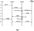
- the picture 3 is a timing diagram illustrating an example implementation of a local read-and-add atomic instruction within the framework of the example of processor of the figure 1 .
- the shared cache memory closest to the cores is that of level 2 (L2).
- the local atomic instructions are then allocated to the cache memories L2 whose management circuit will be configured to process them.
- the core CPUa executes an AFA instruction a1, i, where the parameter a1 is the address of the shared variable and the parameter i is the increment to add to it.
- the instruction is assigned to the shared cache closest to the cores, L2.
- the atomic instruction is transmitted to cache memory L1, which in turn transmits it, at time 11, to cache memory L2.
- the cache memory L2 executes a cached read command LD at the address a1 , which command is associated with a lock command LCK, not of a memory area , but from the local cache line L(a1) assigned to address a1.
- the cache lines are subject to concurrent access by the cores which share this cache memory.
- the cache memory manager can comprise an independent processing unit PU associated with each core, and it is these processing units which compete to initiate accesses to the cache lines. From time t2 access to the cache line L(a1) is reserved exclusively for the core CPUa having executed the atomic instruction. The lock interval is indicated by a bold line.
- the effect of the LD (“LoaD”) read command can be similar to the response of the cache memory to a read instruction of the same name executed by the core.
- This command then causes, according to the usual cache management mechanisms, the verification of the validity of the cache line allocated to the address a1 , in other words if this line is present and has not been invalidated by the consistency management mechanism. If the cache line is invalid or absent (“cache-miss”), the cache manager requests its update (REQ REFILL) to the downstream memory, the downstream memory possibly being the system memory MEM, or a cache memory of higher level (L3), if the processor has one.
- REQ REFILL update
- the new content of the cache line is received from the downstream memory, including the updated value val of the shared variable at the address a1.
- the interval t2 to t3 corresponds to the downstream memory latency.
- the cache line has a non-negligible probability of being valid, in which case the update of the cache line is omitted and the interval t2 to t3 is zero, since the cache memory manager can immediately chain the operations following.
- the cache memory L2 returns the read value val to the cache memory L1 and locally adds the increment i to the value val.
- the cache memory L1 acknowledges the operation to the CPUa core, for example by returning the read value val to the CPUa core.
- the cache memory L2 executes a write command ST ("STore") of the modified variable at the address a1.
- ST write command
- the effect of the ST ("STore") command can be similar to the response of the cache memory to a write instruction of the same name executed by the core.
- This command can then cause, according to the usual cache management mechanisms, the update of the cache line assigned to the address a1 , and the marking of the line as “dirty” (“dirty”). Then, the line is for example placed in a write buffer to the system memory, and it is invalidated in the other L2 cache memories according to the consistency management mechanism.
- the cache line can be unlocked (ULCK) and an acknowledgment can be sent to the cache memory L1.
- the cache memory L2 can empty its write buffer (FLUSH) towards the system memory MEM, or towards a higher level cache memory L3 which passes on the emptying to the system memory.
- the cache line lock interval is shorter than the system memory lock interval in the case of the figure 2 , in particular when the shared variable is up to date in the cache line, avoiding reading the downstream memory between times t2 and t3.
- the classic atomic instructions can be implemented by a second technique, based on a cache coherence protocol according to which the cache line containing the target variable of the instruction atomic is acquired in "exclusive" mode by the core executing the atomic instruction.
- an atomic instruction of local scope limited to a cache level e.g. L2 improves responsiveness by eliminating the exclusive lock mode, requiring the exchange of messages between cache managers of the same level.
- the cache line is not locked in exclusive mode, the cores connected to another cache memory of the same level continue to have access to their cache line in the usual way.
- scopes of atomic instructions are differentiated by families of dedicated atomic instructions of the processor instruction set, i.e. having opcodes (“opcode”) different.
- opcode opcode
- an MMU unit makes it possible to associate various memory transaction modes with ranges of virtual addresses and offers great flexibility for translating ranges of virtual addresses into ranges of physical addresses.
- Memory transaction modes are generally programmable by the operating system in the MMU by setting "attributes" associated with virtual address ranges.
- the MMU unit it is proposed to configure the MMU unit to translate two distinct virtual address ranges to the same physical address range containing the shared variable, and to differentiate the scope of the atomic instruction by setting the transaction mode memory.
- the first range of virtual addresses is associated with the local scope, and is therefore assigned an “in-cache” attribute. Since “cached” mode is generally the default mode, this mode is established without setting any particular attribute in some systems.
- the second range of virtual addresses is associated with the global scope, and is therefore assigned an "out-of-cache" attribute.
- a cache memory controller thus receives the physical address of the variable shared - translated by the MMU from either virtual address range used by the instruction - and an attribute indicative of the scope of the instruction, the value of which depends on the range of virtual addresses used by the instruction.
- the cache memory controller will be able to implement the same generic atomic instruction with a local or global scope depending on whether the virtual address passed as a parameter of the instruction to access the shared variable is in the first or the second range of virtual addresses.
Landscapes
- Engineering & Computer Science (AREA)
- Theoretical Computer Science (AREA)
- Physics & Mathematics (AREA)
- General Engineering & Computer Science (AREA)
- General Physics & Mathematics (AREA)
- Software Systems (AREA)
- Computer Security & Cryptography (AREA)
- Memory System Of A Hierarchy Structure (AREA)
Description
- L'invention est relative aux instructions atomiques de type lecture-modification-écriture mises en oeuvre dans un processeur multi-coeur ayant une mémoire cache partagée, couramment une mémoire cache de niveau 2 ou supérieur.
- La
figure 1 est un schéma simplifié d'un processeur quadri-coeur connecté à une mémoire système MEM, typiquement une mémoire dynamique DDR, par l'intermédiaire de deux niveaux de mémoires cache. Chaque coeur de processeur CPU possède sa propre mémoire cache L1 de niveau 1. Chaque paire de coeurs partage une mémoire cache L2 de niveau 2. Enfin, chaque mémoire cache L2 partage l'accès à la mémoire système MEM. Dans certains processeurs, on peut trouver en outre une mémoire cache de niveau 3 partagée entre les mémoires cache L2. - Chaque mémoire cache comprend un gestionnaire CTRL qui réalise les opérations mises en oeuvre dans la mémoire cache, y compris la gestion de la cohérence (co) entre les mémoires cache. Les coeurs de processeur opèrent généralement sur des adresses virtuelles, alors que les mémoires cache opèrent avec des adresses physiques. Une unité de gestion de mémoire ou MMU est ainsi généralement prévue entre chaque coeur de processeur et le gestionnaire CTRL associé pour traduire les adresses virtuelles en adresses physiques.
- Dans un tel processeur, on peut avoir besoin de partager des données entre des morceaux de code, ou fils de programme, exécutés sur des coeurs différents, ce qui pose des difficultés compte tenu des multiples mémoires cache interposées entre les coeurs qui peuvent stocker des versions différentes des données partagées.
- Pour permettre un partage fiable de données entre plusieurs coeurs, on a souvent recours à des instructions atomiques de type lecture-modification-écriture, par exemple les instructions dites « Fetch-and-Add » (lecture-et-addition, FA) ou « Compare-And-Swap » (comparaison-et-échange, CAS). Ces instructions ont pour caractéristique de produire un effet perçu comme instantané sur le contenu de la mémoire système, en d'autres termes les différentes opérations qui les composent, souvent la lecture d'une variable, la modification de la variable, et la récriture de la variable, sont exécutées en garantissant l'absence d'interférence externe sur la variable entre la lecture et la récriture. Pour garantir l'atomicité, une première technique repose sur un verrouillage de la mémoire système, interdisant tout accès à la mémoire, ou à une zone de la mémoire, par d'autres processus, même si ces processus n'accèdent pas à la variable concernée par la séquence de lecture-modification-écriture.
- Une autre technique repose sur un protocole de cohérence de cache selon lequel la ligne de cache contenant la variable cible de l'instruction atomique est acquise en mode « exclusif » par le coeur exécutant l'instruction. Cette acquisition entraîne l'invalidation de la ligne dans les autres mémoires cache, en interdisant en outre aux autres coeurs d'y accéder, et ainsi d'accéder à la zone associée de la mémoire système, jusqu'à ce que le mode exclusif soit levé par le coeur l'ayant acquis.
- Cette technique limite l'interdiction d'accès à seulement la zone mémoire correspondant à la ligne de cache, mais elle est complexe à réaliser, et présente des restrictions sur l'alignement des données.
- Les deux techniques ont pour résultat de temporairement interdire l'accès à la variable partagée en mémoire, l'une utilisant un mécanisme mis en oeuvre au niveau de la mémoire système, l'autre un mécanisme mis en oeuvre au niveau des mémoires cache.
-
US 7 996 632 B1 divulgue un processeur configuré pour contrôler l'exécution d'instructions atomiques dans un cache. -
US 2013/061020 A1 décrit un système remplaçant la cohérence totale à l'échelle du système par une cohérence partielle. Par exemple, chaque couple processeur-dispositif du système peut être cohérent. Cependant, chaque paire processeur-dispositif peut ne pas être cohérente par rapport aux autres paires processeur-dispositif, comme dans un système entièrement cohérent. - On prévoit de façon générale un processeur multi-coeurs selon la revendication 1. Des modes de réalisations préférentiels sont définis dans les revendications 2 à 4.
- Des modes de réalisation seront exposés dans la description suivante, faite à titre non limitatif en relation avec les figures jointes parmi lesquelles :
- la
figure 1 , précédemment décrite, est un schéma simplifié d'un processeur quadri-coeur comprenant deux niveaux de mémoires cache ; - la
figure 2 est un chronogramme illustrant une mise en oeuvre d'une instruction atomique classique de lecture-et-addition, de portée globale ; et - la
figure 3 est un chronogramme illustrant une mise en oeuvre d'une instruction atomique de lecture-et-addition de portée locale. - La
figure 2 illustre par un chronogramme une mise en oeuvre d'une instruction atomique classique de lecture-et-addition, à titre d'exemple, dans un système du type de lafigure 1 et utilisant la méthode classique de verrouillage de la mémoire système évoquée ci-dessus. L'instruction est notée AFAU, pour Atomic Fetch-and-Add, le suffixe « U » signifiant hors-cache (« Uncached »), c'est-à-dire effective au niveau de la mémoire MEM. Une telle instruction prend comme paramètres l'adresse de la variable partagée et l'incrément à lui ajouter. L'instruction place le coeur en attente d'un acquittement, par exemple le retour de la valeur de la variable partagée avant sa modification. - A un instant t0, un coeur CPUa exécute une instruction AFAU a1, i, où le paramètre a1 est l'adresse de la variable partagée et le paramètre i est l'incrément à lui ajouter. Les opérations atomiques peuvent être déléguées à l'une des mémoires cache, par exemple celle la plus proche de la mémoire système, L2, dont le circuit de gestion peut être pourvu d'une unité de traitement PU conçue pour mettre en oeuvre les opérations.
- Ainsi, à l'instant t0, l'instruction atomique est transmise à la mémoire cache L1, qui la transmet à son tour, à l'instant 11, à la mémoire cache L2.
- A un instant t2, en réponse à l'instruction atomique, la mémoire cache L2 exécute une commande LDU de lecture hors-cache (« LoaD Uncached ») à l'adresse a1, laquelle commande est associée à une commande de verrouillage LCK de la zone mémoire contenant l'adresse a1. La mémoire MEM réagit en verrouillant la zone, signifiant qu'à partir de l'instant t2 l'accès à la zone mémoire est réservé exclusivement au coeur CPUa ayant exécuté l'instruction atomique. L'intervalle de verrouillage est indiqué par un trait gras.
- En outre, l'exécution d'une telle commande hors-cache active la gestion de cohérence des mémoires cache, par exemple en provoquant l'invalidation (INVAL a1) de la ligne de cache attribuée à l'adresse a1 dans toutes les mémoires cache. Ainsi, un autre coeur qui accède en lecture à la variable provoque un rafraîchissement de sa mémoire cache avec la variable à jour dans la mémoire système. Si un tel accès a lieu pendant que la zone mémoire est verrouillée, il est mis en attente du déverrouillage de la zone mémoire.
- A un instant t3, en réponse à la commande de lecture LDU, la mémoire renvoie la valeur val de la variable stockée à l'adresse a1. Il peut s'écouler un nombre relativement important de cycles d'horloge entre l'exécution de la commande LDU et le renvoi de la valeur val.
- A un instant t4, la mémoire cache L2 renvoie la valeur lue val à la mémoire cache L1 et ajoute localement l'incrément i à la valeur val.
- A un instant t5, la mémoire cache L1 renvoie la valeur lue val au coeur CPUa tandis que la mémoire cache L2 exécute une commande STU d'écriture hors-cache (« STore Uncached ») de la valeur modifiée de la variable à l'adresse a1, laquelle commande est associée à une commande de déverrouillage ULCK de la zone mémoire contenant l'adresse a1.
- A un instant t6, en réponse à la commande STU, la mémoire système renvoie à la mémoire cache L2 un signal d'acquittement ACK indiquant la fin du verrouillage. Il peut s'écouler un nombre relativement important de cycles d'horloge entre l'exécution de la commande STU et le renvoi du signal d'acquittement. La mémoire système déverrouille alors la zone mémoire contenant l'adresse a1.
- A partir de l'instant t6, les autres coeurs ont accès à la variable partagée à jour dans la mémoire système. Si un autre coeur a demandé la lecture de la variable partagée entre les instants t2 et t6, la variable ne lui est renvoyée qu'à partir de l'instant t6.
- Les effets des commandes LDU et STU exécutées dans la mémoire cache L2, plus précisément par le gestionnaire de la mémoire cache, peuvent être similaires aux réponses de la mémoire cache à des instructions de même nom exécutées par le coeur. Cela signifie que la ligne de cache attribuée à l'adresse a1 est mise à jour par ces instructions. Ainsi, après l'exécution de la commande d'écriture STU, la ligne de cache est à jour avec la valeur courante en mémoire de la variable.
- L'intervalle de verrouillage de la mémoire système, indiqué en trait gras, peut être relativement important, du fait que la latence de la mémoire système peut être comptée en centaines de cycles de l'horloge des coeurs. Cette latence intervient deux fois pour chaque instruction atomique, une fois pour la commande de lecture LDU et une autre fois pour la commande d'écriture STU. Pendant que la mémoire système est verrouillée, aucun autre processus n'y a accès et est mis en attente, même si le processus n'accède pas à la variable partagée. On peut verrouiller des zones partielles de la mémoire, correspondant par exemple à des banques mémoire, mais ces zones restent relativement grandes de sorte que leur verrouillage est pénalisant pour les performances du système.
- Dans des processeurs du type de la
figure 1 , on peut trouver des mémoires cache qui sont partagées par plusieurs coeurs, par exemple deux ou quatre pour une mémoire cache de niveau 2. Certains processeurs peuvent avoir une mémoire cache de niveau 3 qui est partagée par encore plus de coeurs. Par ailleurs, dans de nombreuses situations, on peut intervenir sur la répartition des fils de programme sur les coeurs de manière que des fils interdépendants soient affectés à des coeurs partageant une même mémoire cache. Par exemple, dans lafigure 1 , on affectera deux fils interdépendants respectivement aux coeurs CPUa et CPUb, ou CPUc et CPUd. - En outre, une variable partagée par un groupe de fils de programme interdépendants n'a généralement aucune utilité pour d'autres processus, notamment des processus qui pourraient être exécutés sur des coeurs qui ne partagent pas la mémoire cache. En d'autres termes, les autres processus n'ont pas besoin d'accéder à une valeur à jour de la variable partagée.
- Sur ce constat, on propose d'introduire dans le jeu d'instructions du processeur des instructions atomiques de portée locale. Plus spécifiquement, une telle instruction n'est atomique que jusqu'à un niveau de mémoire cache intermédiaire. Dans un processeur comprenant plusieurs niveaux de mémoires cache partagées, on préfèrera attribuer l'instruction atomique de portée locale à la mémoire cache partagée la plus proche des coeurs.
- Le jeu d'instructions du processeur comporte, en plus d'une famille d'instructions atomiques classiques (que l'on qualifiera de portée globale), une famille d'instructions atomiques de portée locale homologues. Ainsi, par exemple, si le processeur comporte une instruction atomique lecture-et-addition classique AFAU (Add-and-Fetch Uncached), on introduit son instruction homologue de portée locale ou « en-cache » AFA.
- Alors, les instructions atomiques globales classiques pourront être utilisées dans des fils interdépendants exécutés sur des coeurs quelconques qui ne partagent pas forcément la même mémoire cache, tandis que les nouvelles instructions atomiques locales seront utilisées dans des fils interdépendants exécutés sur des coeurs qui partagent une mémoire cache.
- La
figure 3 est un chronogramme illustrant un exemple de mise en oeuvre d'une instruction atomique de lecture-et-addition locale dans le cadre de l'exemple de processeur de lafigure 1 . Dans le processeur de lafigure 1 , la mémoire cache partagée la plus proche des coeurs est celle de niveau 2 (L2). Les instructions atomiques locales sont alors attribuées aux mémoires cache L2 dont le circuit de gestion sera configuré pour les traiter. - A un instant t0, le coeur CPUa exécute une instruction AFA a1, i, où le paramètre a1 est l'adresse de la variable partagée et le paramètre i est l'incrément à lui ajouter. L'instruction est attribuée à la mémoire cache partagée la plus proche des coeurs, L2.
- Ainsi, à l'instant t0, l'instruction atomique est transmise à la mémoire cache L1, qui la transmet à son tour, à l'instant 11, à la mémoire cache L2.
- A un instant t2, en réponse à l'instruction atomique, la mémoire cache L2 exécute une commande LD de lecture en-cache à l'adresse a1, laquelle commande est associée à une commande de verrouillage LCK, non pas d'une zone mémoire, mais de la ligne de cache locale L(a1) attribuée à l'adresse a1.
- Les lignes de cache sont soumises à des accès concurrents par les coeurs qui partagent cette mémoire cache. En pratique, comme cela est représenté dans la
figure 1 pour les mémoires cache L2, le gestionnaire de la mémoire cache peut comprendre une unité de traitement indépendante PU associée à chaque coeur, et ce sont ces unités de traitement qui sont en concurrence pour initier des accès aux lignes de cache. A partir de l'instant t2 l'accès à la ligne de cache L(a1) est réservé exclusivement au coeur CPUa ayant exécuté l'instruction atomique. L'intervalle de verrouillage est indiqué par un trait gras. - L'effet de la commande de lecture LD (« LoaD ») peut être similaire à la réponse de la mémoire cache à une instruction de lecture de même nom exécutée par le coeur. Cette commande provoque alors, selon les mécanismes de gestion de cache habituels, la vérification de la validité de la ligne de cache attribuée à l'adresse a1, en d'autres termes si cette ligne est présente et n'a pas été invalidée par le mécanisme de gestion de cohérence. Si la ligne de cache est invalide ou absente (« cache-miss »), le gestionnaire de cache requiert sa mise à jour (REQ REFILL) à la mémoire aval, la mémoire aval pouvant être la mémoire système MEM, ou une mémoire cache de niveau supérieur (L3), si le processeur en comporte une.
- A un instant t3, si une mise à jour a été requise, le nouveau contenu de la ligne de cache est reçu de la mémoire aval, incluant la valeur val à jour de la variable partagée à l'adresse a1.
- Lors d'une mise à jour de ligne de cache, l'intervalle t2 à t3 correspond à la latence de la mémoire aval. Cependant, la ligne de cache a une probabilité non négligeable d'être valide, auquel cas la mise à jour de la ligne de cache est omise et l'intervalle t2 à t3 est nul, puisque le gestionnaire de mémoire cache peut enchaîner immédiatement les opérations suivantes.
- A un instant t4, la mémoire cache L2 renvoie la valeur lue val à la mémoire cache L1 et ajoute localement l'incrément i à la valeur val.
- A un instant t5, la mémoire cache L1 acquitte l'opération auprès du coeur CPUa, par exemple en renvoyant la valeur lue val au coeur CPUa. La mémoire cache L2 exécute une commande ST d'écriture (« STore ») de la variable modifiée à l'adresse a1. L'effet de la commande ST (« STore ») peut être similaire à la réponse de la mémoire cache à une instruction d'écriture de même nom exécutée par le coeur. Cette commande peut alors provoquer, selon les mécanismes de gestion de cache habituels, la mise à jour de la ligne de cache attribuée à l'adresse a1, et le marquage de la ligne comme « sale » (« dirty »). Alors, la ligne est par exemple mise dans un tampon d'écriture vers la mémoire système, et elle est invalidée dans les autres mémoires cache L2 selon le mécanisme de gestion de cohérence.
- Selon une variante, on peut omettre d'invalider la ligne dans les autres mémoires cache de même niveau, puisque la variable modifiée est partagée seulement entre les coeurs connectés à la même mémoire cache. En d'autres termes, les autres coeurs pourront continuer à accéder sans latence aux données dans la ligne de leur mémoire cache et n'accéderont en principe pas à la variable partagée obsolète dans cette ligne.
- A un instant t6, dès que la variable partagée est à jour dans la ligne de cache, la ligne de cache peut être déverrouillée (ULCK) et un acquittement peut être envoyé vers la mémoire cache L1. A partir de cet instant, la mémoire cache L2 peut vider son tampon d'écriture (FLUSH) vers la mémoire système MEM, ou vers une mémoire cache de niveau supérieur L3 qui répercute le vidage vers la mémoire système.
- On s'aperçoit que l'intervalle de verrouillage de la ligne de cache est plus court que l'intervalle de verrouillage de la mémoire système dans le cas de la
figure 2 , notamment lorsque la variable partagée est à jour dans la ligne de cache, évitant la lecture de la mémoire aval entre les instants t2 et t3. - Un gain remarquable provient du fait que ce n'est pas la mémoire système qui est verrouillée, mais seulement une ligne de cache attribuée à l'adresse de la variable partagée. Les accès à d'autres lignes de cache et à l'ensemble de la mémoire système restent autorisés aux coeurs concurrents pendant les opérations atomiques locales.
- Comme on l'a précédemment évoqué, dans certaines architectures de processeur, les instructions atomiques classiques peuvent être mises en oeuvre par une deuxième technique, reposant sur un protocole de cohérence de cache selon lequel la ligne de cache contenant la variable cible de l'instruction atomique est acquise en mode « exclusif » par le coeur exécutant l'instruction atomique. Dans une telle architecture, une instruction atomique de portée locale limitée à un niveau de cache (par exemple L2) améliore la réactivité par l'élimination du mode de verrouillage exclusif, nécessitant l'échange de messages entre les gestionnaires de cache de même niveau. En outre, comme la ligne de cache n'est pas verrouillée en mode exclusif, les coeurs reliés à une autre mémoire cache de même niveau continuent à avoir accès à leur ligne de cache de façon habituelle.
- Dans ce qui précède, on a supposé que les portées des instructions atomiques (locale ou globale) étaient différenciées par des familles d'instructions atomiques dédiées du jeu d'instructions du processeur, c'est-à-dire ayant des codes opération (« opcode ») différents. Selon un autre mode de réalisation, on peut utiliser la même famille d'instructions atomiques, qu'on qualifiera de générique, et différencier la portée en utilisant des fonctionnalités classiquement offertes par une unité de gestion de mémoire MMU. En effet, une unité MMU permet d'associer divers modes de transaction mémoire à des plages d'adresses virtuelles et offre une grande souplesse pour traduire des plages d'adresses virtuelles vers des plages d'adresses physiques. Les modes des transactions mémoire sont généralement programmables par le système d'exploitation dans l'unité MMU en réglant des « attributs » associés aux plages d'adresses virtuelles.
- Dans ce contexte, on propose de configurer l'unité MMU pour traduire deux plages d'adresses virtuelles distinctes vers une même plage d'adresses physiques contenant la variable partagée, et de différencier la portée de l'instruction atomique en réglant le mode des transactions mémoire. La première plage d'adresses virtuelles est associée à la portée locale, et on lui affecte pour cela un attribut « en-cache ». Le mode « en-cache » étant généralement le mode par défaut, ce mode est établi sans régler d'attribut particulier dans certains systèmes. La deuxième plage d'adresses virtuelles est associée à la portée globale, et on lui affecte pour cela un attribut « hors-cache ».
- Les valeurs des attributs sont généralement véhiculées sur des lignes supplémentaires des bus d'adresses pour être prises en compte notamment par les contrôleurs de mémoire cache. Un contrôleur de mémoire cache reçoit ainsi l'adresse physique de la variable partagée - traduite par l'unité MMU à partir de l'une ou l'autre plage d'adresses virtuelles utilisée par l'instruction - et un attribut indicatif de la portée de l'instruction, dont la valeur dépend de la plage d'adresses virtuelles utilisée par l'instruction.
- Avec cette configuration, le contrôleur de mémoire cache pourra mettre en oeuvre une même instruction atomique générique avec une portée locale ou globale selon que l'adresse virtuelle passée en paramètre de l'instruction pour accéder à la variable partagée se trouve dans la première ou la deuxième plage d'adresses virtuelles.
Claims (4)
- Processeur multi-coeurs comprenant :• une mémoire cache (L2 CACHE) partagée par un groupe de plusieurs coeurs (CPUa, CPUb) configurés pour déléguer des instructions atomiques à la mémoire cache ;• dans son jeu d'instructions, une instruction atomique de lecture-modification-écriture (AFAU), prenant comme paramètre une adresse mémoire d'une variable partagée, l'instruction atomique ayant une portée globale ;• un gestionnaire de mémoire cache (CTRL) configuré pour recevoir et traiter chaque instruction atomique globale exécutée par un coeur donné du groupe en verrouillant globalement une plage d'adresses contenant l'adresse de la variable partagée, de sorte à interdire l'accès à la variable partagée à tout autre coeur pendant l'exécution de l'instruction atomique globale ;le gestionnaire de mémoire cache étant configuré pour :
dans lequel l'instruction atomique a en outre une portée locale, le gestionnaire de mémoire cache étant configuré pour traiter chaque instruction atomique locale exécutée par un coeur donné du groupe en verrouillant localement une ligne de cache associée à l'adresse de la variable partagée, tout en autorisant un accès à la variable partagée à des coeurs connectés à une autre mémoire cache de même niveau partagée par un autre groupe de plusieurs coeurs (CPUc, CPUd) pendant l'exécution de l'instruction atomique locale ;utiliser un protocole de cohérence de cache pour mettre en oeuvre les instructions atomiques globales, et pour, lors de l'exécution d'une instruction atomique locale, verrouiller localement la ligne de cache sans invalider ni verrouiller une ligne de cache homologue dans l'autre mémoire cache de même niveau, ouverrouiller une zone d'une mémoire système contenant la variable partagée pendant l'exécution d'une instruction atomique globale, et pour, lors de l'exécution d'une instruction atomique locale, accéder à la variable dans la ligne de cache et ne verrouiller aucune zone de la mémoire système. - Processeur selon la revendication 1, dans lequel les portées globale et locale des instructions atomiques sont mises en oeuvre par deux instructions respectives dédiées du jeu d'instructions du processeur (AFAU, AFA).
- Processeur selon la revendication 1, dans lequel les portées globale et locale des instructions atomiques sont mises en oeuvre par une même instruction du jeu d'instructions, et sont différenciées par l'utilisation de deux plages d'adresses virtuelles distinctes associées à une même plage d'adresses physiques contenant la variable partagée, le processeur comprenant une unité de gestion de mémoire (MMU) qui effectue une traduction des adresses virtuelles en adresses physiques, et qui associe un attribut « hors-cache » à la plage d'adresses virtuelles associée à la portée globale.
- Processeur selon la revendication 1, dans lequel l'instruction atomique locale est une instruction de lecture-et-addition, ayant en outre comme paramètre une valeur d'incrément (i), le gestionnaire de mémoire cache étant configuré pour ajouter l'incrément à la variable.
Applications Claiming Priority (1)
| Application Number | Priority Date | Filing Date | Title |
|---|---|---|---|
| FR1651869A FR3048526B1 (fr) | 2016-03-07 | 2016-03-07 | Instruction atomique de portee limitee a un niveau de cache intermediaire |
Publications (2)
| Publication Number | Publication Date |
|---|---|
| EP3217288A1 EP3217288A1 (fr) | 2017-09-13 |
| EP3217288B1 true EP3217288B1 (fr) | 2023-01-25 |
Family
ID=56801631
Family Applications (1)
| Application Number | Title | Priority Date | Filing Date |
|---|---|---|---|
| EP17157413.0A Active EP3217288B1 (fr) | 2016-03-07 | 2017-02-22 | Instruction atomique de portée locale limitée à un niveau de cache intermédiaire |
Country Status (4)
| Country | Link |
|---|---|
| US (1) | US11144480B2 (fr) |
| EP (1) | EP3217288B1 (fr) |
| CN (1) | CN107168680B (fr) |
| FR (1) | FR3048526B1 (fr) |
Families Citing this family (8)
| Publication number | Priority date | Publication date | Assignee | Title |
|---|---|---|---|---|
| KR102372423B1 (ko) * | 2017-05-16 | 2022-03-10 | 한국전자통신연구원 | 파라미터 공유 장치 및 방법 |
| CN108647154A (zh) * | 2018-05-14 | 2018-10-12 | 国网山东省电力公司阳谷县供电公司 | 一种在集中器中进行参数修改的方法 |
| US11182159B2 (en) * | 2020-02-26 | 2021-11-23 | Google Llc | Vector reductions using shared scratchpad memory |
| US11467962B2 (en) * | 2020-09-02 | 2022-10-11 | SiFive, Inc. | Method for executing atomic memory operations when contested |
| CN113836050A (zh) * | 2021-09-30 | 2021-12-24 | 龙芯中科技术股份有限公司 | 访存控制方法、装置、设备及可读存储介质 |
| US11934318B2 (en) * | 2022-06-07 | 2024-03-19 | XConn Technologies Holdings, Inc. | Multi-host memory sharing |
| US12204462B2 (en) * | 2022-12-02 | 2025-01-21 | SiFive, Inc. | Downgrading a permission associated with data stored in a cache |
| WO2025062169A1 (fr) * | 2023-09-19 | 2025-03-27 | Synthara Ag | Ordinateur in-memory |
Citations (2)
| Publication number | Priority date | Publication date | Assignee | Title |
|---|---|---|---|---|
| US6631447B1 (en) * | 1993-03-18 | 2003-10-07 | Hitachi, Ltd. | Multiprocessor system having controller for controlling the number of processors for which cache coherency must be guaranteed |
| US20130061020A1 (en) * | 2011-09-01 | 2013-03-07 | Qualcomm Incorporated | Computer System with Processor Local Coherency for Virtualized Input/Output |
Family Cites Families (18)
| Publication number | Priority date | Publication date | Assignee | Title |
|---|---|---|---|---|
| JP2500101B2 (ja) * | 1992-12-18 | 1996-05-29 | インターナショナル・ビジネス・マシーンズ・コーポレイション | 共用変数の値を更新する方法 |
| US6430657B1 (en) * | 1998-10-12 | 2002-08-06 | Institute For The Development Of Emerging Architecture L.L.C. | Computer system that provides atomicity by using a tlb to indicate whether an exportable instruction should be executed using cache coherency or by exporting the exportable instruction, and emulates instructions specifying a bus lock |
| AU2001236793A1 (en) * | 2000-02-25 | 2001-09-03 | Sun Microsystems, Inc. | Apparatus and method for maintaining high snoop traffic throughput and preventing cache data eviction during an atomic operation |
| US7971030B2 (en) * | 2002-08-07 | 2011-06-28 | Mmagix Technology Limited | Method for using multiple processing resources which share multiple co-processor resources |
| US6920532B2 (en) * | 2002-11-05 | 2005-07-19 | Newisys, Inc. | Cache coherence directory eviction mechanisms for modified copies of memory lines in multiprocessor systems |
| US7194587B2 (en) * | 2003-04-24 | 2007-03-20 | International Business Machines Corp. | Localized cache block flush instruction |
| US7996632B1 (en) * | 2006-12-22 | 2011-08-09 | Oracle America, Inc. | Device for misaligned atomics for a highly-threaded x86 processor |
| US8281075B2 (en) * | 2009-04-14 | 2012-10-02 | International Business Machines Corporation | Processor system and methods of triggering a block move using a system bus write command initiated by user code |
| US8117399B2 (en) * | 2009-05-07 | 2012-02-14 | Freescale Semiconductor, Inc. | Processing of coherent and incoherent accesses at a uniform cache |
| US9086973B2 (en) * | 2009-06-09 | 2015-07-21 | Hyperion Core, Inc. | System and method for a cache in a multi-core processor |
| US8095617B2 (en) * | 2009-06-30 | 2012-01-10 | Oracle America Inc. | Caching data in a cluster computing system which avoids false-sharing conflicts |
| US8788794B2 (en) * | 2010-12-07 | 2014-07-22 | Advanced Micro Devices, Inc. | Programmable atomic memory using stored atomic procedures |
| US9122476B2 (en) * | 2010-12-07 | 2015-09-01 | Advanced Micro Devices, Inc. | Programmable atomic memory using hardware validation agent |
| US20120304178A1 (en) * | 2011-05-24 | 2012-11-29 | International Business Machines Corporation | Concurrent reduction optimizations for thieving schedulers |
| US20130159812A1 (en) * | 2011-12-16 | 2013-06-20 | Advanced Micro Devices, Inc. | Memory architecture for read-modify-write operations |
| US8694706B2 (en) * | 2012-04-27 | 2014-04-08 | Oracle International Corporation | System and method for NUMA-aware locking using lock cohorts |
| US9218289B2 (en) * | 2012-08-06 | 2015-12-22 | Qualcomm Incorporated | Multi-core compute cache coherency with a release consistency memory ordering model |
| US9734063B2 (en) * | 2014-02-27 | 2017-08-15 | École Polytechnique Fédérale De Lausanne (Epfl) | Scale-out non-uniform memory access |
-
2016
- 2016-03-07 FR FR1651869A patent/FR3048526B1/fr active Active
-
2017
- 2017-02-22 EP EP17157413.0A patent/EP3217288B1/fr active Active
- 2017-03-07 CN CN201710191989.2A patent/CN107168680B/zh active Active
- 2017-03-07 US US15/452,073 patent/US11144480B2/en active Active
Patent Citations (2)
| Publication number | Priority date | Publication date | Assignee | Title |
|---|---|---|---|---|
| US6631447B1 (en) * | 1993-03-18 | 2003-10-07 | Hitachi, Ltd. | Multiprocessor system having controller for controlling the number of processors for which cache coherency must be guaranteed |
| US20130061020A1 (en) * | 2011-09-01 | 2013-03-07 | Qualcomm Incorporated | Computer System with Processor Local Coherency for Virtualized Input/Output |
Non-Patent Citations (1)
| Title |
|---|
| ANONYMOUS: "Lock (computer science) - Wikipedia", 17 January 2012 (2012-01-17), XP055370138, Retrieved from the Internet <URL:https://en.wikipedia.org/w/index.php?title=Lock_(computer_science)&oldid=471818463> [retrieved on 20170508] * |
Also Published As
| Publication number | Publication date |
|---|---|
| CN107168680A (zh) | 2017-09-15 |
| EP3217288A1 (fr) | 2017-09-13 |
| US11144480B2 (en) | 2021-10-12 |
| FR3048526A1 (fr) | 2017-09-08 |
| CN107168680B (zh) | 2023-09-12 |
| FR3048526B1 (fr) | 2023-01-06 |
| US20170255571A1 (en) | 2017-09-07 |
Similar Documents
| Publication | Publication Date | Title |
|---|---|---|
| EP3217288A1 (fr) | Instruction atomique de portée locale limitée à un niveau de cache intermédiaire | |
| AU2010337318B2 (en) | Mechanisms to accelerate transactions using buffered stores | |
| US11614959B2 (en) | Coherence protocol for hardware transactional memory in shared memory using non volatile memory with log and no lock | |
| US8271730B2 (en) | Handling of write access requests to shared memory in a data processing apparatus | |
| US8255626B2 (en) | Atomic commit predicated on consistency of watches | |
| US20080022054A1 (en) | Object based conflict detection in a software transactional memory | |
| US20090019247A1 (en) | Bufferless Transactional Memory with Runahead Execution | |
| KR20080076981A (ko) | 무한 트랜잭션 메모리 시스템 | |
| US20090198694A1 (en) | Resolving conflicts in a transactional execution model of a multiprocessor system | |
| FR2677472A1 (fr) | Unite de controle pour memoire cache de second niveau. | |
| US7356670B2 (en) | Data processing system | |
| US20050015637A1 (en) | Data processing system | |
| US20100318747A1 (en) | Atomic memory operation cache protocol with opportunistic combining | |
| GB2523804A (en) | Transactional memory support | |
| US20100287342A1 (en) | Processing of coherent and incoherent accesses at a uniform cache | |
| US11586462B2 (en) | Memory access request for a memory protocol | |
| US20230244604A1 (en) | Contention tracking for latency reduction of exclusive operations | |
| FR2808902A1 (fr) | Systeme de pre-extraction speculative de donnees dans un systeme de processeur d'execution non ordonnee d'instructions | |
| US7409503B2 (en) | Register file systems and methods for employing speculative fills | |
| US11809319B2 (en) | Contention tracking for processor cache management | |
| EP3519971B1 (fr) | Appareil et procédé pour fournir un ensemble atomique d'accès à des données | |
| EP1739561A1 (fr) | Cohérence de cache dans un système multiprocesseurs à mémoire partagée | |
| WO2014056534A1 (fr) | Antémémoire de données sensible au contexte | |
| US20070088896A1 (en) | Arithmetic processing unit and method for operating cache | |
| FR2631472A1 (fr) | Procede de transmission d'informations dans un systeme informatique, notamment un systeme a antememoires |
Legal Events
| Date | Code | Title | Description |
|---|---|---|---|
| PUAI | Public reference made under article 153(3) epc to a published international application that has entered the european phase |
Free format text: ORIGINAL CODE: 0009012 |
|
| STAA | Information on the status of an ep patent application or granted ep patent |
Free format text: STATUS: THE APPLICATION HAS BEEN PUBLISHED |
|
| AK | Designated contracting states |
Kind code of ref document: A1 Designated state(s): AL AT BE BG CH CY CZ DE DK EE ES FI FR GB GR HR HU IE IS IT LI LT LU LV MC MK MT NL NO PL PT RO RS SE SI SK SM TR |
|
| AX | Request for extension of the european patent |
Extension state: BA ME |
|
| STAA | Information on the status of an ep patent application or granted ep patent |
Free format text: STATUS: REQUEST FOR EXAMINATION WAS MADE |
|
| 17P | Request for examination filed |
Effective date: 20180306 |
|
| RBV | Designated contracting states (corrected) |
Designated state(s): AL AT BE BG CH CY CZ DE DK EE ES FI FR GB GR HR HU IE IS IT LI LT LU LV MC MK MT NL NO PL PT RO RS SE SI SK SM TR |
|
| STAA | Information on the status of an ep patent application or granted ep patent |
Free format text: STATUS: EXAMINATION IS IN PROGRESS |
|
| 17Q | First examination report despatched |
Effective date: 20180612 |
|
| RIC1 | Information provided on ipc code assigned before grant |
Ipc: G06F 9/52 20060101ALI20220701BHEP Ipc: G06F 9/30 20060101ALI20220701BHEP Ipc: G06F 12/0815 20160101ALI20220701BHEP Ipc: G06F 12/0811 20160101ALI20220701BHEP Ipc: G06F 12/0804 20160101AFI20220701BHEP |
|
| GRAP | Despatch of communication of intention to grant a patent |
Free format text: ORIGINAL CODE: EPIDOSNIGR1 |
|
| STAA | Information on the status of an ep patent application or granted ep patent |
Free format text: STATUS: GRANT OF PATENT IS INTENDED |
|
| INTG | Intention to grant announced |
Effective date: 20220908 |
|
| GRAS | Grant fee paid |
Free format text: ORIGINAL CODE: EPIDOSNIGR3 |
|
| GRAA | (expected) grant |
Free format text: ORIGINAL CODE: 0009210 |
|
| STAA | Information on the status of an ep patent application or granted ep patent |
Free format text: STATUS: THE PATENT HAS BEEN GRANTED |
|
| AK | Designated contracting states |
Kind code of ref document: B1 Designated state(s): AL AT BE BG CH CY CZ DE DK EE ES FI FR GB GR HR HU IE IS IT LI LT LU LV MC MK MT NL NO PL PT RO RS SE SI SK SM TR |
|
| REG | Reference to a national code |
Ref country code: GB Ref legal event code: FG4D Free format text: NOT ENGLISH |
|
| REG | Reference to a national code |
Ref country code: CH Ref legal event code: EP |
|
| REG | Reference to a national code |
Ref country code: DE Ref legal event code: R096 Ref document number: 602017065689 Country of ref document: DE |
|
| REG | Reference to a national code |
Ref country code: AT Ref legal event code: REF Ref document number: 1546349 Country of ref document: AT Kind code of ref document: T Effective date: 20230215 Ref country code: IE Ref legal event code: FG4D Free format text: LANGUAGE OF EP DOCUMENT: FRENCH |
|
| REG | Reference to a national code |
Ref country code: NL Ref legal event code: FP |
|
| REG | Reference to a national code |
Ref country code: LT Ref legal event code: MG9D |
|
| REG | Reference to a national code |
Ref country code: AT Ref legal event code: MK05 Ref document number: 1546349 Country of ref document: AT Kind code of ref document: T Effective date: 20230125 |
|
| PG25 | Lapsed in a contracting state [announced via postgrant information from national office to epo] |
Ref country code: RS Free format text: LAPSE BECAUSE OF FAILURE TO SUBMIT A TRANSLATION OF THE DESCRIPTION OR TO PAY THE FEE WITHIN THE PRESCRIBED TIME-LIMIT Effective date: 20230125 Ref country code: PT Free format text: LAPSE BECAUSE OF FAILURE TO SUBMIT A TRANSLATION OF THE DESCRIPTION OR TO PAY THE FEE WITHIN THE PRESCRIBED TIME-LIMIT Effective date: 20230525 Ref country code: NO Free format text: LAPSE BECAUSE OF FAILURE TO SUBMIT A TRANSLATION OF THE DESCRIPTION OR TO PAY THE FEE WITHIN THE PRESCRIBED TIME-LIMIT Effective date: 20230425 Ref country code: LV Free format text: LAPSE BECAUSE OF FAILURE TO SUBMIT A TRANSLATION OF THE DESCRIPTION OR TO PAY THE FEE WITHIN THE PRESCRIBED TIME-LIMIT Effective date: 20230125 Ref country code: LT Free format text: LAPSE BECAUSE OF FAILURE TO SUBMIT A TRANSLATION OF THE DESCRIPTION OR TO PAY THE FEE WITHIN THE PRESCRIBED TIME-LIMIT Effective date: 20230125 Ref country code: HR Free format text: LAPSE BECAUSE OF FAILURE TO SUBMIT A TRANSLATION OF THE DESCRIPTION OR TO PAY THE FEE WITHIN THE PRESCRIBED TIME-LIMIT Effective date: 20230125 Ref country code: ES Free format text: LAPSE BECAUSE OF FAILURE TO SUBMIT A TRANSLATION OF THE DESCRIPTION OR TO PAY THE FEE WITHIN THE PRESCRIBED TIME-LIMIT Effective date: 20230125 Ref country code: AT Free format text: LAPSE BECAUSE OF FAILURE TO SUBMIT A TRANSLATION OF THE DESCRIPTION OR TO PAY THE FEE WITHIN THE PRESCRIBED TIME-LIMIT Effective date: 20230125 |
|
| PG25 | Lapsed in a contracting state [announced via postgrant information from national office to epo] |
Ref country code: SE Free format text: LAPSE BECAUSE OF FAILURE TO SUBMIT A TRANSLATION OF THE DESCRIPTION OR TO PAY THE FEE WITHIN THE PRESCRIBED TIME-LIMIT Effective date: 20230125 Ref country code: PL Free format text: LAPSE BECAUSE OF FAILURE TO SUBMIT A TRANSLATION OF THE DESCRIPTION OR TO PAY THE FEE WITHIN THE PRESCRIBED TIME-LIMIT Effective date: 20230125 Ref country code: IS Free format text: LAPSE BECAUSE OF FAILURE TO SUBMIT A TRANSLATION OF THE DESCRIPTION OR TO PAY THE FEE WITHIN THE PRESCRIBED TIME-LIMIT Effective date: 20230525 Ref country code: GR Free format text: LAPSE BECAUSE OF FAILURE TO SUBMIT A TRANSLATION OF THE DESCRIPTION OR TO PAY THE FEE WITHIN THE PRESCRIBED TIME-LIMIT Effective date: 20230426 Ref country code: FI Free format text: LAPSE BECAUSE OF FAILURE TO SUBMIT A TRANSLATION OF THE DESCRIPTION OR TO PAY THE FEE WITHIN THE PRESCRIBED TIME-LIMIT Effective date: 20230125 |
|
| REG | Reference to a national code |
Ref country code: DE Ref legal event code: R097 Ref document number: 602017065689 Country of ref document: DE |
|
| PG25 | Lapsed in a contracting state [announced via postgrant information from national office to epo] |
Ref country code: SM Free format text: LAPSE BECAUSE OF FAILURE TO SUBMIT A TRANSLATION OF THE DESCRIPTION OR TO PAY THE FEE WITHIN THE PRESCRIBED TIME-LIMIT Effective date: 20230125 Ref country code: RO Free format text: LAPSE BECAUSE OF FAILURE TO SUBMIT A TRANSLATION OF THE DESCRIPTION OR TO PAY THE FEE WITHIN THE PRESCRIBED TIME-LIMIT Effective date: 20230125 Ref country code: MC Free format text: LAPSE BECAUSE OF FAILURE TO SUBMIT A TRANSLATION OF THE DESCRIPTION OR TO PAY THE FEE WITHIN THE PRESCRIBED TIME-LIMIT Effective date: 20230125 Ref country code: LU Free format text: LAPSE BECAUSE OF NON-PAYMENT OF DUE FEES Effective date: 20230222 Ref country code: EE Free format text: LAPSE BECAUSE OF FAILURE TO SUBMIT A TRANSLATION OF THE DESCRIPTION OR TO PAY THE FEE WITHIN THE PRESCRIBED TIME-LIMIT Effective date: 20230125 Ref country code: DK Free format text: LAPSE BECAUSE OF FAILURE TO SUBMIT A TRANSLATION OF THE DESCRIPTION OR TO PAY THE FEE WITHIN THE PRESCRIBED TIME-LIMIT Effective date: 20230125 Ref country code: CZ Free format text: LAPSE BECAUSE OF FAILURE TO SUBMIT A TRANSLATION OF THE DESCRIPTION OR TO PAY THE FEE WITHIN THE PRESCRIBED TIME-LIMIT Effective date: 20230125 |
|
| PG25 | Lapsed in a contracting state [announced via postgrant information from national office to epo] |
Ref country code: SK Free format text: LAPSE BECAUSE OF FAILURE TO SUBMIT A TRANSLATION OF THE DESCRIPTION OR TO PAY THE FEE WITHIN THE PRESCRIBED TIME-LIMIT Effective date: 20230125 |
|
| PLBE | No opposition filed within time limit |
Free format text: ORIGINAL CODE: 0009261 |
|
| STAA | Information on the status of an ep patent application or granted ep patent |
Free format text: STATUS: NO OPPOSITION FILED WITHIN TIME LIMIT |
|
| 26N | No opposition filed |
Effective date: 20231026 |
|
| PG25 | Lapsed in a contracting state [announced via postgrant information from national office to epo] |
Ref country code: SI Free format text: LAPSE BECAUSE OF FAILURE TO SUBMIT A TRANSLATION OF THE DESCRIPTION OR TO PAY THE FEE WITHIN THE PRESCRIBED TIME-LIMIT Effective date: 20230125 |
|
| PG25 | Lapsed in a contracting state [announced via postgrant information from national office to epo] |
Ref country code: IT Free format text: LAPSE BECAUSE OF FAILURE TO SUBMIT A TRANSLATION OF THE DESCRIPTION OR TO PAY THE FEE WITHIN THE PRESCRIBED TIME-LIMIT Effective date: 20230125 |
|
| PG25 | Lapsed in a contracting state [announced via postgrant information from national office to epo] |
Ref country code: BG Free format text: LAPSE BECAUSE OF FAILURE TO SUBMIT A TRANSLATION OF THE DESCRIPTION OR TO PAY THE FEE WITHIN THE PRESCRIBED TIME-LIMIT Effective date: 20230125 |
|
| PG25 | Lapsed in a contracting state [announced via postgrant information from national office to epo] |
Ref country code: BG Free format text: LAPSE BECAUSE OF FAILURE TO SUBMIT A TRANSLATION OF THE DESCRIPTION OR TO PAY THE FEE WITHIN THE PRESCRIBED TIME-LIMIT Effective date: 20230125 |
|
| PGFP | Annual fee paid to national office [announced via postgrant information from national office to epo] |
Ref country code: NL Payment date: 20250226 Year of fee payment: 9 |
|
| PGFP | Annual fee paid to national office [announced via postgrant information from national office to epo] |
Ref country code: DE Payment date: 20250312 Year of fee payment: 9 |
|
| PGFP | Annual fee paid to national office [announced via postgrant information from national office to epo] |
Ref country code: IE Payment date: 20250226 Year of fee payment: 9 |
|
| PGFP | Annual fee paid to national office [announced via postgrant information from national office to epo] |
Ref country code: BE Payment date: 20250226 Year of fee payment: 9 Ref country code: CH Payment date: 20250313 Year of fee payment: 9 |
|
| PGFP | Annual fee paid to national office [announced via postgrant information from national office to epo] |
Ref country code: FR Payment date: 20250219 Year of fee payment: 9 |
|
| PGFP | Annual fee paid to national office [announced via postgrant information from national office to epo] |
Ref country code: GB Payment date: 20250226 Year of fee payment: 9 |
|
| PG25 | Lapsed in a contracting state [announced via postgrant information from national office to epo] |
Ref country code: CY Free format text: LAPSE BECAUSE OF FAILURE TO SUBMIT A TRANSLATION OF THE DESCRIPTION OR TO PAY THE FEE WITHIN THE PRESCRIBED TIME-LIMIT; INVALID AB INITIO Effective date: 20170222 |
|
| PG25 | Lapsed in a contracting state [announced via postgrant information from national office to epo] |
Ref country code: HU Free format text: LAPSE BECAUSE OF FAILURE TO SUBMIT A TRANSLATION OF THE DESCRIPTION OR TO PAY THE FEE WITHIN THE PRESCRIBED TIME-LIMIT; INVALID AB INITIO Effective date: 20170222 |
|
| PG25 | Lapsed in a contracting state [announced via postgrant information from national office to epo] |
Ref country code: TR Free format text: LAPSE BECAUSE OF FAILURE TO SUBMIT A TRANSLATION OF THE DESCRIPTION OR TO PAY THE FEE WITHIN THE PRESCRIBED TIME-LIMIT Effective date: 20230125 |