EP3214760A2 - Feed-forward filtering device and associated method - Google Patents
Feed-forward filtering device and associated method Download PDFInfo
- Publication number
- EP3214760A2 EP3214760A2 EP17155232.6A EP17155232A EP3214760A2 EP 3214760 A2 EP3214760 A2 EP 3214760A2 EP 17155232 A EP17155232 A EP 17155232A EP 3214760 A2 EP3214760 A2 EP 3214760A2
- Authority
- EP
- European Patent Office
- Prior art keywords
- signal
- filtering
- noise
- output signal
- generate
- Prior art date
- Legal status (The legal status is an assumption and is not a legal conclusion. Google has not performed a legal analysis and makes no representation as to the accuracy of the status listed.)
- Granted
Links
Images





Classifications
-
- H—ELECTRICITY
- H04—ELECTRIC COMMUNICATION TECHNIQUE
- H04L—TRANSMISSION OF DIGITAL INFORMATION, e.g. TELEGRAPHIC COMMUNICATION
- H04L25/00—Baseband systems
- H04L25/02—Details ; arrangements for supplying electrical power along data transmission lines
- H04L25/03—Shaping networks in transmitter or receiver, e.g. adaptive shaping networks
- H04L25/03993—Noise whitening
-
- H—ELECTRICITY
- H03—ELECTRONIC CIRCUITRY
- H03H—IMPEDANCE NETWORKS, e.g. RESONANT CIRCUITS; RESONATORS
- H03H11/00—Networks using active elements
- H03H11/02—Multiple-port networks
- H03H11/38—One-way transmission networks, i.e. unilines
-
- H—ELECTRICITY
- H03—ELECTRONIC CIRCUITRY
- H03H—IMPEDANCE NETWORKS, e.g. RESONANT CIRCUITS; RESONATORS
- H03H1/00—Constructional details of impedance networks whose electrical mode of operation is not specified or applicable to more than one type of network
- H03H1/02—RC networks, e.g. filters
-
- H—ELECTRICITY
- H03—ELECTRONIC CIRCUITRY
- H03H—IMPEDANCE NETWORKS, e.g. RESONANT CIRCUITS; RESONATORS
- H03H11/00—Networks using active elements
- H03H11/02—Multiple-port networks
- H03H11/04—Frequency selective two-port networks
- H03H11/0422—Frequency selective two-port networks using transconductance amplifiers, e.g. gmC filters
- H03H11/0461—Current mode filters
-
- H—ELECTRICITY
- H03—ELECTRONIC CIRCUITRY
- H03H—IMPEDANCE NETWORKS, e.g. RESONANT CIRCUITS; RESONATORS
- H03H11/00—Networks using active elements
- H03H11/02—Multiple-port networks
- H03H11/04—Frequency selective two-port networks
- H03H11/12—Frequency selective two-port networks using amplifiers with feedback
- H03H11/1213—Frequency selective two-port networks using amplifiers with feedback using transistor amplifiers
-
- H—ELECTRICITY
- H03—ELECTRONIC CIRCUITRY
- H03H—IMPEDANCE NETWORKS, e.g. RESONANT CIRCUITS; RESONATORS
- H03H21/00—Adaptive networks
-
- H—ELECTRICITY
- H04—ELECTRIC COMMUNICATION TECHNIQUE
- H04L—TRANSMISSION OF DIGITAL INFORMATION, e.g. TELEGRAPHIC COMMUNICATION
- H04L25/00—Baseband systems
- H04L25/02—Details ; arrangements for supplying electrical power along data transmission lines
- H04L25/03—Shaping networks in transmitter or receiver, e.g. adaptive shaping networks
- H04L25/03828—Arrangements for spectral shaping; Arrangements for providing signals with specified spectral properties
- H04L25/03834—Arrangements for spectral shaping; Arrangements for providing signals with specified spectral properties using pulse shaping
- H04L25/03847—Shaping by selective switching of amplifying elements
-
- H—ELECTRICITY
- H04—ELECTRIC COMMUNICATION TECHNIQUE
- H04L—TRANSMISSION OF DIGITAL INFORMATION, e.g. TELEGRAPHIC COMMUNICATION
- H04L47/00—Traffic control in data switching networks
- H04L47/50—Queue scheduling
- H04L47/52—Queue scheduling by attributing bandwidth to queues
- H04L47/522—Dynamic queue service slot or variable bandwidth allocation
-
- G—PHYSICS
- G10—MUSICAL INSTRUMENTS; ACOUSTICS
- G10K—SOUND-PRODUCING DEVICES; METHODS OR DEVICES FOR PROTECTING AGAINST, OR FOR DAMPING, NOISE OR OTHER ACOUSTIC WAVES IN GENERAL; ACOUSTICS NOT OTHERWISE PROVIDED FOR
- G10K2210/00—Details of active noise control [ANC] covered by G10K11/178 but not provided for in any of its subgroups
- G10K2210/10—Applications
- G10K2210/108—Communication systems, e.g. where useful sound is kept and noise is cancelled
-
- H—ELECTRICITY
- H03—ELECTRONIC CIRCUITRY
- H03H—IMPEDANCE NETWORKS, e.g. RESONANT CIRCUITS; RESONATORS
- H03H11/00—Networks using active elements
- H03H11/02—Multiple-port networks
- H03H11/04—Frequency selective two-port networks
- H03H11/12—Frequency selective two-port networks using amplifiers with feedback
- H03H11/126—Frequency selective two-port networks using amplifiers with feedback using a single operational amplifier
- H03H11/1269—Filters using the operational amplifier pole
-
- H—ELECTRICITY
- H04—ELECTRIC COMMUNICATION TECHNIQUE
- H04L—TRANSMISSION OF DIGITAL INFORMATION, e.g. TELEGRAPHIC COMMUNICATION
- H04L25/00—Baseband systems
- H04L25/02—Details ; arrangements for supplying electrical power along data transmission lines
- H04L25/03—Shaping networks in transmitter or receiver, e.g. adaptive shaping networks
- H04L25/03006—Arrangements for removing intersymbol interference
- H04L25/03012—Arrangements for removing intersymbol interference operating in the time domain
- H04L25/03019—Arrangements for removing intersymbol interference operating in the time domain adaptive, i.e. capable of adjustment during data reception
- H04L25/03057—Arrangements for removing intersymbol interference operating in the time domain adaptive, i.e. capable of adjustment during data reception with a recursive structure
Definitions
- the present invention relates to a filtering device, and more particularly, to a feed-forward filtering device and an associated method according to the pre-characterizing clauses of claims 1, 10, 13 and 15.
- a Resistor-Capacitor (RC) low-pass filter is the most common filter used for filtering out undesired noise, but resistors cost a larger area in more advanced IC technology. Therefore, a filtering technique which can reduce the area of the filter for an RC based filter while also being able to effectively filter out undesired noise is required.
- RC Resistor-Capacitor
- One of the objectives of the present invention is to provide a filtering device and an associated filtering method to solve the abovementioned problems.
- a filtering device comprising a low pass-filter (LPF), a noise estimation circuit, and a first combining circuit.
- the low pass-filter is arranged to receive and filter a pre-filtering signal to generate an output signal of the filtering device;
- the noise estimation circuit is arranged to estimate an estimated noise signal according to the output signal and the pre-filtering signal; and
- a first combining circuit is arranged to subtract the estimated noise signal from an input signal of the filtering device to generate the pre-filtering signal.
- a filtering device comprising a low-pass filter (LPF), a feedback circuit and a resistor circuit.
- the low-pass filter is arranged to receive and filter a pre-filtering signal from an interconnection node to generate an output signal of the filtering device;
- the feedback circuit is arranged to receive the output signal to generate a feedback signal;
- the resistor circuit is coupled between an input signal of the filtering device and the feedback signal to generate the pre-filtering signal at the interconnection node; wherein the input signal, the pre-filtering signal and the output signal are voltage signals.
- a filtering method comprises: performing a low-pass filtering (LPF) operation upon a pre-filtering signal to generate an output signal; estimating a estimated noise signal according to the output signal and the pre-filtering signal; and subtracting the estimated noise signal from an input signal to generate the pre-filtering signal.
- LPF low-pass filtering
- a filtering method comprises: performing a low-pass filtering (LPF) operation upon a pre-filtering signal from an interconnection node to generate an output signal; generating a feedback signal according to the output signal; and utilizing a resistor circuit coupled between an input signal and the feedback signal to generate the pre-filtering signal at the interconnection node; wherein the input signal, the pre-filtering signal and the output signal are voltage signals.
- LPF low-pass filtering
- FIG. 1 is a diagram illustrating a filtering device 100 according to an embodiment of the present invention.
- the filtering device 100 may be a feed-forward filtering device.
- the filtering device 100 comprises a low-pass filter (LPF) 101, a noise estimation circuit 102 and a combining circuit 103, wherein the low-pass filter 101 receives and filters a pre-filtering signal S pre to generate an output signal S out , the noise estimation circuit 102 generates an estimated noise signal S noise according to the output signal S out and the pre-filtering signal S pre , and the combining circuit 103 subtracts the estimated noise signal S noise from an input signal S in to generate the pre-filtering signal S pre .
- LPF low-pass filter
- the pre-filtering signal S pre , the output signal S out and the input signal S in illustrated here can be referred to as voltage signals (e.g. V pre , V out , and V in ) or current signals (e.g. I pre , I out , and I in ).
- the noise can be greatly reduced by subtracting the estimated noise signal S noise generated by the noise estimation circuit 102 from the input signal S in when the input signal S in enters the circuit.
- FIG. 2 is a diagram illustrating the noise estimation circuit 102 of the filtering device 100.
- the noise estimation circuit 102 may be implemented using amplifying circuits 201 and 202, and a combining circuit 203.
- the gain of the amplifying circuit 201 is ⁇ 1, while the gain of the amplifying circuit 202 is ⁇ 2.
- the combining circuit 203 subtracts the amplified output signal S amp.out from the amplified pre-filtering signal S amp.pre to generate the estimated noise signal S noise as shown in FIG. 2 .
- the configuration of the noise estimation circuit 102 shown in FIG. 2 is for illustrative purposes only.
- both the amplifying circuits 201 and 202 can be replaced with a unity-gain buffer.
- the amplifying circuits 201 and 202 can be optional.
- the combining circuit 203 subtracts the amplified output signal S amp.out from the pre-filtering signal S pre , where the pre-filtering signal S pre is received by the combining circuit 203.
- the amplifying circuits 202 is used and the output signal S out is directly fed into the combining circuit 203, and the combining circuit 203 can subtract the output signal S out from the amplified pre-filtering signal S amp.pre , where the output signal S out is received by the combining circuit 203.
- neither the amplifying circuit 201 nor the amplifying circuit 202 is used.
- the combining circuit 203 subtracts the output signal S out from the pre-filtering signal S pre , where the output signal S out and the pre-filtering signal S pre are received by the combining circuit 203.
- the estimated noise signal S noise After subtracting the output signal S out (or the amplified output signal S amp.out ) which is filtered by the low-pass filter 101 from the pre-filtering signal S pre (or the amplified pre-filtering signal S amp.pre ) which has not been filtered, the estimated noise signal S noise can be extracted.
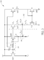
- FIG. 3 is a circuit diagram of a filtering device 300 implemented according to the filtering devices shown in FIG. 1 and FIG. 2 .
- the pre-filtering signal S pre , the output signal S out , the estimated noise signal S noise and the input signal S in are referred to as current signals, i.e. an pre-filtering signal I pre , an output signal I out , an estimated noise signal I noise and an input signal I in as marked in FIG. 3 .
- I pre an output signal I out
- I in marked in FIG. 3 .
- the filtering device 300 is composed of a plurality of current mirrors including transistors MP1, MP2, MP3 , MP4, MN1 and MN2, where MP1, MP2, MP3 and MP4 are P-channel metal oxide semiconductor (PMOS) transistors, and MN1 and MN2 are N-channel metal oxide semiconductor (NMOS) transistors.
- MP1, MP2, MP3 and MP4 are P-channel metal oxide semiconductor (PMOS) transistors
- MN1 and MN2 are N-channel metal oxide semiconductor (NMOS) transistors.
- the filtering device 300 comprises a low-pass filter 301, a noise estimation circuit 302 and a combining circuit 303, wherein the low-pass filter 301 is a passive Resistor-Capacitor filter composed of a resistor R1 and a capacitor C1, the noise estimation circuit 302 is composed of the transistor MP3, the transistor MN1 and a combining circuit 302_1 implemented by a node N2 for draining and receiving current, and the combining circuit 303 is implemented by a node N1 in this embodiment.
- the transistor MP3 included in the noise estimation circuit 302 is referred to as the amplifying circuit 202 for amplifying a current signal I pre generated by the transistor MP2 according to its channel width or length.
- the channel width of the transistor MP3 may be configured to be ⁇ 2 times as large as the channel width of the transistor MP2. In this way, the current generated by the transistor MP3 is ⁇ 2*I pre when the current generated by the transistor MP2 is I pre .
- the low-pass filter 301 is coupled between the transistor MP1 and MP2.
- the pre-filtering signal I pre is received by the low-pass filter 301 via a node N3.
- the low-pass filter 301 filters the pre-filtering signal I pre to generate a filtered signal at a node N4.
- the transistor MP1 receives the filtered signal to generate the output signal I out .
- the transistor MP4 replicates the current of the output signal I out and also produces the output signal I out .
- the output signal I out flows via the drain terminals of the transistor MP4 and MN2, where in one embodiment, the channel width of the transistor MP4 is same as that of the transistor MP1 to mirror the current signal I out directly on the drain terminal of the transistor MP4.
- the channel width of the transistor MN1 By configuring the channel width of the transistor MN1 to be ⁇ 1 times as large as that of the transistor MN2, i.e. when the channel width of the transistor MN2 is marked as 1, the channel width of the transistor MN1 is marked as ⁇ 1, a current ⁇ 1*I out is generated from a drain terminal of the transistor MN1.
- the channel width of the transistor MP4 and that of the transistor MN2, as well as the gain provided by the transistor MP4 and the gain provided by the transistor MN2, should be subject to circuit designs and thus can be varying accordingly.
- an estimated noise signal I noise is drained from the node N2 included in the combining circuit 203_1 to the node N1 included in the combining circuit 303, and a current signal I in is thus drained from the node N1 according to the estimated noise signal I noise and the pre-filtering I pre .
- FIG. 4 is a diagram illustrating a filtering device 400, which is a simplified circuit of that shown in FIG. 2 .
- the filtering device 400 comprises a low-pass filter (LPF) 401, a combining circuit 402, and amplifying circuits 403 and 404, wherein the gain of the amplifying circuit 403 is 1/(1+ ⁇ 2), while the gain of the amplifying circuit 404 is ⁇ 1.
- the filtering device 300 can be thus simplified by combining the combining circuits 303 and 302_1 shown in FIG. 3 .
- FIG. 5 is a diagram illustrating a filtering device 500, which is a simplified circuit of that shown in FIG. 3 .
- the filtering device 500 is composed of a plurality of current mirrors including transistors MP1', MP2', MP3', MN1' and MN2', where MP1', MP2' and MP3' are PMOS transistors, and MN1' and MN2' are NMOS transistors.
- the difference between the embodiments of FIG. 3 and FIG. 5 is that the two transistors MP2 and MP3 shown in FIG. 3 are combined as a single transistor MP2' based on the concept of combining two circuits as shown in FIG. 4 .
- the filtering device 500 After combining the transistor MP2 and MP3 as the transistor MP2', the filtering device 500 thus comprises a combining circuit 501 implemented by a node N5 whose function is similar/identical with the combining circuit 401 for combining the current I in and ⁇ 1*I out .
- the filtering device comprises a amplifying circuit 502 implemented by the transistor MN1' whose function is similar/identical with the amplifying circuit 404 for amplifying the output current I out by ⁇ 1.
- the low-pass filter 301 generates a filtered signal at the node N4.
- the transistor MP1' receives the filtered signal to generate the output signal I out .
- the transistor MP3' replicates the current of the output signal I out and also produces the output signal I out .
- the output signal I out flows via the drain terminals of the transistors MP3' and MN2'.
- FIG. 3 and FIG. 5 are implemented by a plurality of current mirrors; however, both implementations are hard to be applied to filtering voltage signals.
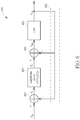
- the filtering device 400 shown in FIG. 4 can be simplified to the circuit 600 shown in FIG. 6 .
- the filtering device 600 comprises a low-pass filter (LPF) 601, a feedback path 602, combining circuits 603 and 604, and an amplifying circuit 605, wherein the low-pass filter 601 is arranged to receive and filter the pre-filtering S pre to generate the output signal S out which is sent to the combining circuits 603 and 604 through the feedback path 602.
- the combining circuit 603 is arranged to subtract the output signal S out from the input signal S in to generate a signal S x .
- the amplifying circuit 605 is arranged to amplify the signal S x to generate a signal S y
- the combining circuit 604 is arranged to combine the signal S y and the output signal S out to generate the pre-filtering signal S pre .
- the input signal S in , the signals S x and S y , the pre-filtering signal S pre and the output signal S out are referred to as voltage signals in this embodiment.
- the following equation (6) describes the relation between the pre-filtering signal S pre and the output signal S out according to the embodiment in FIG. 6 .
- Spre Sout * ⁇ 1 ⁇ 2 + 1 + 1
- FIG. 7 is a diagram illustrating a filtering device 700 implemented according to the filtering device shown in FIG. 6 .
- the pre-filtering signal S pre , the output signal S out , and the input signal S in are referred to as voltage signals, i.e. the pre-filtering signal V pre , the output signal V out , and the input signal V in as marked in FIG. 7 .
- the filtering device 700 comprises a low-pass filter 701, a feedback circuit 702 and a resistor circuit 703, wherein the low-pass filter 701 is a passive Resistor-Capacitor filter including a resistor R2 and a capacitor C2, the feedback circuit 702 comprises a feedback buffer 712, and the resistor circuit 703 comprises a plurality of resistors Rx and Ry. More specifically, the low-pass filter 701 is arranged to receive and filter the pre-filtering signal V pre to generate an output signal V out .
- the feedback buffer 712 included in the feedback circuit 702 is arranged to send the output signal V out to the resistor circuit 703.
- the resistors Rx and Ry are connected in series and coupled between the output signal V out and an input signal V in is arranged to serve as a voltage divider that divides the voltage to generate the pre-filtering signal Vp re shown in FIG. 7 .
- the following equations describe the relation between the input signal V in and the output signal V out according to the embodiment in FIG. 7 .
- H(s) is the transfer function of the low-pass filter 701.
- the -3dB frequency of the filtering device 700 can be reduced by 1/(1+ ⁇ 2) to decrease the noise effectively.
- the filtering device 700 can therefore be configured to further comprise a buffer 704 coupled between the input signal V in and the resistor Rx, which increases the driving ability of input signal V in , as shown in FIG. 7 .
- the low-pass filters 301, 501, and 701 are implemented by passive Resistor-Capacitor filters. This is only for illustrative purposes and not a limitation of the present invention. In other embodiments, the low-pass filter can be implemented by other circuits such as an active low-pass filter.
- embodiments of the present invention disclose filtering devices employing the feed forward technique to subtract noise from the input signal when the input signal enters the circuit.
- noise can be effectively decreased without increasing the resistance of a resistor included in a low-pass filter, and the consumed area for a low-pass filter in an integrated circuit can also be effectively limited.
Landscapes
- Engineering & Computer Science (AREA)
- Computer Networks & Wireless Communication (AREA)
- Signal Processing (AREA)
- Power Engineering (AREA)
- Physics & Mathematics (AREA)
- Spectroscopy & Molecular Physics (AREA)
- Amplifiers (AREA)
- Networks Using Active Elements (AREA)
- Noise Elimination (AREA)
- Filters That Use Time-Delay Elements (AREA)
Abstract
Description
- The present invention relates to a filtering device, and more particularly, to a feed-forward filtering device and an associated method according to the pre-characterizing clauses of
claims 1, 10, 13 and 15. - In an integrated circuit (IC) design, circuitry comprising hundreds of circuit blocks has to be designed within a limited area. A Resistor-Capacitor (RC) low-pass filter is the most common filter used for filtering out undesired noise, but resistors cost a larger area in more advanced IC technology. Therefore, a filtering technique which can reduce the area of the filter for an RC based filter while also being able to effectively filter out undesired noise is required.
- One of the objectives of the present invention is to provide a filtering device and an associated filtering method to solve the abovementioned problems.
- According to a first aspect of the present invention, a filtering device is disclosed, wherein the filtering device comprises a low pass-filter (LPF), a noise estimation circuit, and a first combining circuit. The low pass-filter is arranged to receive and filter a pre-filtering signal to generate an output signal of the filtering device; the noise estimation circuit is arranged to estimate an estimated noise signal according to the output signal and the pre-filtering signal; and a first combining circuit is arranged to subtract the estimated noise signal from an input signal of the filtering device to generate the pre-filtering signal.
- According to a second aspect of the present invention, a filtering device is disclosed, comprising a low-pass filter (LPF), a feedback circuit and a resistor circuit. The low-pass filter is arranged to receive and filter a pre-filtering signal from an interconnection node to generate an output signal of the filtering device; the feedback circuit is arranged to receive the output signal to generate a feedback signal; and the resistor circuit is coupled between an input signal of the filtering device and the feedback signal to generate the pre-filtering signal at the interconnection node; wherein the input signal, the pre-filtering signal and the output signal are voltage signals.
- According to a third aspect of the present invention, a filtering method is disclosed, wherein the filtering method comprises: performing a low-pass filtering (LPF) operation upon a pre-filtering signal to generate an output signal; estimating a estimated noise signal according to the output signal and the pre-filtering signal; and subtracting the estimated noise signal from an input signal to generate the pre-filtering signal.
- According to a fourth aspect of the present invention, a filtering method is disclosed, wherein the filtering method comprises: performing a low-pass filtering (LPF) operation upon a pre-filtering signal from an interconnection node to generate an output signal; generating a feedback signal according to the output signal; and utilizing a resistor circuit coupled between an input signal and the feedback signal to generate the pre-filtering signal at the interconnection node; wherein the input signal, the pre-filtering signal and the output signal are voltage signals.
- In the following, the invention is further illustrated by way of example, taking reference to the accompanying drawings. Thereof
- FIG. 1
- is a diagram illustrating a filtering device according to an embodiment of the present invention,
- FIG. 2
- is a diagram illustrating a noise estimation circuit of the filtering device of
FIG. 1 according to an embodiment of the present invention, - FIG. 3
- is a circuit diagram of a filtering device implemented according to the filtering devices shown in
FIG. 1 andFIG. 2 , - FIG. 4
- is a diagram illustrating a simplified circuit of the filtering device shown in
FIG. 2 , - FIG. 5
- is a diagram illustrating a simplified circuit of the filtering device shown in
FIG. 3 , - FIG. 6
- is a diagram illustrating a simplified circuit of the filtering device shown in
FIG. 4 , and - FIG. 7
- is a diagram illustrating a filtering device implemented according to the filtering device shown in
FIG. 6 . - Certain terms are used throughout the description and following claims to refer to particular components. As one skilled in the art will appreciate, manufacturers may refer to a component by different names. This document does not intend to distinguish between components that differ in name but not function. In the following description and in the claims, the terms "include" and "comprise" are used in an open-ended fashion, and thus should not be interpreted as a close-ended term such as "consist of". Also, the term "couple" is intended to mean either an indirect or direct electrical connection. Accordingly, if one device is coupled to another device, that connection may be through a direct electrical connection, or through an indirect electrical connection via other devices and connections.
-
FIG. 1 is a diagram illustrating afiltering device 100 according to an embodiment of the present invention. Thefiltering device 100 may be a feed-forward filtering device. As shown inFIG. 1 , thefiltering device 100 comprises a low-pass filter (LPF) 101, anoise estimation circuit 102 and a combiningcircuit 103, wherein the low-pass filter 101 receives and filters a pre-filtering signal Spre to generate an output signal Sout, thenoise estimation circuit 102 generates an estimated noise signal Snoise according to the output signal Sout and the pre-filtering signal Spre, and the combiningcircuit 103 subtracts the estimated noise signal Snoise from an input signal Sin to generate the pre-filtering signal Spre. It should be noted that the pre-filtering signal Spre, the output signal Sout and the input signal Sin illustrated here can be referred to as voltage signals (e.g. Vpre, Vout, and Vin) or current signals (e.g. Ipre, Iout, and Iin). The noise can be greatly reduced by subtracting the estimated noise signal Snoise generated by thenoise estimation circuit 102 from the input signal Sin when the input signal Sin enters the circuit. -
FIG. 2 is a diagram illustrating thenoise estimation circuit 102 of thefiltering device 100. As shown inFIG. 2 , thenoise estimation circuit 102 may be implemented using amplifyingcircuits circuit 203. The gain of theamplifying circuit 201 is β1, while the gain of theamplifying circuit 202 is β2. The amplifyingcircuit 201 is arranged to amplify the output signal Sout to generate an amplified output signal Samp.out, where Samp.out =β1·Sout. The amplifyingcircuit 202 is arranged to amplify the pre-filtering signal Spre to generate an amplified pre-filtering signal Samp.pre, where Samp.pre =β2·Spre . The combiningcircuit 203 subtracts the amplified output signal Samp.out from the amplified pre-filtering signal Samp.pre to generate the estimated noise signal Snoise as shown inFIG. 2 . It should be noted that the configuration of thenoise estimation circuit 102 shown inFIG. 2 is for illustrative purposes only. In one embodiment, both theamplifying circuits circuits circuit 201 is used and the pre-filtering signal Spre is directly fed into the combiningcircuit 203, and the combiningcircuit 203 subtracts the amplified output signal Samp.out from the pre-filtering signal Spre, where the pre-filtering signal Spre is received by the combiningcircuit 203. For another example, only the amplifyingcircuits 202 is used and the output signal Sout is directly fed into the combiningcircuit 203, and the combiningcircuit 203 can subtract the output signal Sout from the amplified pre-filtering signal Samp.pre, where the output signal Sout is received by the combiningcircuit 203. For a further example, neither the amplifyingcircuit 201 nor the amplifyingcircuit 202 is used. The combiningcircuit 203 subtracts the output signal Sout from the pre-filtering signal Spre, where the output signal Sout and the pre-filtering signal Spre are received by the combiningcircuit 203. - After subtracting the output signal Sout (or the amplified output signal Samp.out) which is filtered by the low-
pass filter 101 from the pre-filtering signal Spre (or the amplified pre-filtering signal Samp.pre) which has not been filtered, the estimated noise signal Snoise can be extracted. -
FIG. 3 is a circuit diagram of afiltering device 300 implemented according to the filtering devices shown inFIG. 1 andFIG. 2 . In the embodiment ofFIG. 3 , the pre-filtering signal Spre, the output signal Sout, the estimated noise signal Snoise and the input signal Sin are referred to as current signals, i.e. an pre-filtering signal Ipre, an output signal Iout, an estimated noise signal Inoise and an input signal Iin as marked inFIG. 3 . As shown inFIG. 3 , thefiltering device 300 is composed of a plurality of current mirrors including transistors MP1, MP2, MP3 , MP4, MN1 and MN2, where MP1, MP2, MP3 and MP4 are P-channel metal oxide semiconductor (PMOS) transistors, and MN1 and MN2 are N-channel metal oxide semiconductor (NMOS) transistors. Thefiltering device 300 comprises a low-pass filter 301, anoise estimation circuit 302 and a combiningcircuit 303, wherein the low-pass filter 301 is a passive Resistor-Capacitor filter composed of a resistor R1 and a capacitor C1, thenoise estimation circuit 302 is composed of the transistor MP3, the transistor MN1 and a combining circuit 302_1 implemented by a node N2 for draining and receiving current, and the combiningcircuit 303 is implemented by a node N1 in this embodiment. As mentioned in the embodiment ofFIG. 2 , the transistor MP3 included in thenoise estimation circuit 302 is referred to as the amplifyingcircuit 202 for amplifying a current signal Ipre generated by the transistor MP2 according to its channel width or length. The channel width of the transistor MP3 may be configured to be β2 times as large as the channel width of the transistor MP2. In this way, the current generated by the transistor MP3 is β2*Ipre when the current generated by the transistor MP2 is Ipre. The low-pass filter 301 is coupled between the transistor MP1 and MP2. The pre-filtering signal Ipre is received by the low-pass filter 301 via a node N3. The low-pass filter 301 filters the pre-filtering signal Ipre to generate a filtered signal at a node N4. The transistor MP1 receives the filtered signal to generate the output signal Iout. With the function of a current mirror, the transistor MP4 replicates the current of the output signal Iout and also produces the output signal Iout. The output signal Iout flows via the drain terminals of the transistor MP4 and MN2, where in one embodiment, the channel width of the transistor MP4 is same as that of the transistor MP1 to mirror the current signal Iout directly on the drain terminal of the transistor MP4. By configuring the channel width of the transistor MN1 to be β1 times as large as that of the transistor MN2, i.e. when the channel width of the transistor MN2 is marked as 1, the channel width of the transistor MN1 is marked as β1, a current β1*Iout is generated from a drain terminal of the transistor MN1. Please note that the channel width of the transistor MP4 and that of the transistor MN2, as well as the gain provided by the transistor MP4 and the gain provided by the transistor MN2, should be subject to circuit designs and thus can be varying accordingly. In accordance with the Kirchhoff Circuit Laws, an estimated noise signal Inoise is drained from the node N2 included in the combining circuit 203_1 to the node N1 included in the combiningcircuit 303, and a current signal Iin is thus drained from the node N1 according to the estimated noise signal Inoise and the pre-filtering Ipre. - The following current equations which illustrate the Kirchhoff Circuit Laws can explain the embodiment of
FIG. 3 clearly.


pass filter 301. - According to the equations (1)-(3) illustrated above, the relation between the output signal Iout and the input signal Iin can be written as follows:

filtering device 300 is:
- According to equation (5), the -3dB frequency of the
filtering device 300 can be reduced by 1+β2 when β1=β2, which can decrease the noise effectively. It should be noted that, in this embodiment, Δβ must be greater than -1, or a positive feedback might occur in thefiltering device 300. -
FIG. 4 is a diagram illustrating afiltering device 400, which is a simplified circuit of that shown inFIG. 2 . Referring toFIG. 2 again, by combining the combiningcircuits filtering device 100 can be simplified accordingly. As shown inFIG. 4 , thefiltering device 400 comprises a low-pass filter (LPF) 401, a combiningcircuit 402, and amplifyingcircuits circuit 403 is 1/(1+β2), while the gain of the amplifyingcircuit 404 is β1. Based on the same theory, thefiltering device 300 can be thus simplified by combining the combiningcircuits 303 and 302_1 shown inFIG. 3 . -
FIG. 5 is a diagram illustrating afiltering device 500, which is a simplified circuit of that shown inFIG. 3 . As shown inFIG. 5 , thefiltering device 500 is composed of a plurality of current mirrors including transistors MP1', MP2', MP3', MN1' and MN2', where MP1', MP2' and MP3' are PMOS transistors, and MN1' and MN2' are NMOS transistors. The difference between the embodiments ofFIG. 3 andFIG. 5 is that the two transistors MP2 and MP3 shown inFIG. 3 are combined as a single transistor MP2' based on the concept of combining two circuits as shown inFIG. 4 . After combining the transistor MP2 and MP3 as the transistor MP2', thefiltering device 500 thus comprises a combiningcircuit 501 implemented by a node N5 whose function is similar/identical with the combiningcircuit 401 for combining the current Iin and β1*Iout. The filtering device comprises a amplifyingcircuit 502 implemented by the transistor MN1' whose function is similar/identical with the amplifyingcircuit 404 for amplifying the output current Iout by β1. As descried in the embodiment ofFIG. 3 , the low-pass filter 301 generates a filtered signal at the node N4. The transistor MP1' receives the filtered signal to generate the output signal Iout. With the function of a current mirror, the transistor MP3' replicates the current of the output signal Iout and also produces the output signal Iout. The output signal Iout flows via the drain terminals of the transistors MP3' and MN2'. Those skilled in the art should readily understand the detailed operation of the circuit shown inFIG. 5 after reading the above paragraphs. A detailed description is therefore omitted here for brevity. - The embodiments of
FIG. 3 andFIG. 5 are implemented by a plurality of current mirrors; however, both implementations are hard to be applied to filtering voltage signals. In practice, a condition β1=β2 is used to simplify thefiltering device 400 for the situation where the input signals Sin, the pre-filtering signal Spre and the output signal Sout are voltage signals instead of current signals. - Under the condition β1=β2, the
filtering device 400 shown inFIG. 4 can be simplified to thecircuit 600 shown inFIG. 6 . Thefiltering device 600 comprises a low-pass filter (LPF) 601, afeedback path 602, combiningcircuits amplifying circuit 605, wherein the low-pass filter 601 is arranged to receive and filter the pre-filtering Spre to generate the output signal Sout which is sent to the combiningcircuits feedback path 602. The combiningcircuit 603 is arranged to subtract the output signal Sout from the input signal Sin to generate a signal Sx. The amplifyingcircuit 605 is arranged to amplify the signal Sx to generate a signal Sy, and the combiningcircuit 604 is arranged to combine the signal Sy and the output signal Sout to generate the pre-filtering signal Spre. It should be noted that the input signal Sin, the signals Sx and Sy, the pre-filtering signal Spre and the output signal Sout are referred to as voltage signals in this embodiment. The following equation (6) describes the relation between the pre-filtering signal Spre and the output signal Sout according to the embodiment inFIG. 6 .
- According to equation (6), a filtering device arranged for filtering voltage signals, instead of current signals, can be easily implemented.
FIG. 7 is a diagram illustrating afiltering device 700 implemented according to the filtering device shown inFIG. 6 . In the embodiment ofFIG. 7 , the pre-filtering signal Spre, the output signal Sout, and the input signal Sin are referred to as voltage signals, i.e. the pre-filtering signal Vpre, the output signal Vout, and the input signal Vin as marked inFIG. 7 . Thefiltering device 700 comprises a low-pass filter 701, afeedback circuit 702 and aresistor circuit 703, wherein the low-pass filter 701 is a passive Resistor-Capacitor filter including a resistor R2 and a capacitor C2, thefeedback circuit 702 comprises afeedback buffer 712, and theresistor circuit 703 comprises a plurality of resistors Rx and Ry. More specifically, the low-pass filter 701 is arranged to receive and filter the pre-filtering signal Vpre to generate an output signal Vout. Thefeedback buffer 712 included in thefeedback circuit 702 is arranged to send the output signal Vout to theresistor circuit 703. The resistors Rx and Ry are connected in series and coupled between the output signal Vout and an input signal Vin is arranged to serve as a voltage divider that divides the voltage to generate the pre-filtering signal Vpre shown inFIG. 7 . The following equations describe the relation between the input signal Vin and the output signal Vout according to the embodiment inFIG. 7 .

pass filter 701. - According to equations (7) and (8), it can be deduced that

- Based on equation (9), the -3dB frequency of the
filtering device 700 can be reduced by 1/(1+ β2) to decrease the noise effectively. - In practice, the input signal Vin might not have enough driving ability; the
filtering device 700 can therefore be configured to further comprise abuffer 704 coupled between the input signal Vin and the resistor Rx, which increases the driving ability of input signal Vin, as shown inFIG. 7 . - It should be noted that, in the embodiments of
FIG. 3 ,FIG. 5 andFIG. 7 , the low-pass filters - Briefly summarized, embodiments of the present invention disclose filtering devices employing the feed forward technique to subtract noise from the input signal when the input signal enters the circuit. In this way, noise can be effectively decreased without increasing the resistance of a resistor included in a low-pass filter, and the consumed area for a low-pass filter in an integrated circuit can also be effectively limited.
Claims (15)
- A filtering device (100, 300), characterized by:a low-pass filter (101, 301), arranged to receive and filter a pre-filtering signal (Spre, Ipre) to generate an output signal (Sout, Iout) of the filtering device (100, 300) ;a noise estimation circuit (102, 302), arranged to generate an estimated noise signal (Snoise, Inoise) according to the output signal (Sout, Iout) and the pre-filtering signal (Spre, Ipre); anda first combining circuit (103, 303), arranged to subtract the estimated noise signal (Snoise, Inoise) from an input signal (Sin, Iin) of the filtering device (100, 300) to generate the pre-filtering signal (Spre, Ipre).
- The filtering device (100) of claim 1, characterized in that the noise estimation circuit (102) comprises:a second combining circuit (203), arranged to subtract the output signal (Sout) from the pre-filtering signal (Spre) to generate the estimated noise signal (Snoise).
- The filtering device (100) of claim 1, characterized in that the noise estimation circuit (102) comprises:an amplifying circuit (201), arranged to amplify the output signal (Sout) by a gain (β 1) to generate an amplified output signal (Samp.out); anda second combining circuit (203), arranged to subtract the amplified output signal (Samp.out) from the pre-filtering signal (Spre) to generate the estimated noise signal (Snoise).
- The filtering device (100) of claim 1, characterized in that the noise estimation circuit (102) comprises:an amplifying circuit (202), arranged to amplify the pre-filtering signal (Spre) by a gain (β 2) to generate an amplified pre-filtering signal (Samp.pre); anda second combining circuit (202), arranged to subtract the output signal (Sout) from the amplified pre-filtering signal (Samp.pre) to generate the estimated noise signal (Snoise).
- The filtering device (100, 300) of claim 1, characterized in that the noise estimation circuit (102, 302) comprises:a first amplifying circuit (201, MN1), arranged to amplify the output signal (Sout, Iout) by a first gain (β 1) to generate an amplified output signal (Samp.out, β 1*Iout);a second amplifying circuit (202, MN3), arranged to amplify the pre-filtering signal (Spre, Ipre) by a second gain (β 2) to generate an amplified pre-filtering signal (Samp.pre, β 2*Ipre); anda second combining circuit (203, 302_1), arranged to subtract the amplified output signal (Samp.out, β 1*Iout) from the amplifiedpre-filtering signal (Samp.pre, β 2*Ipre) to generate the estimated noise signal (Snoise, Inoise).
- The filtering device (100) of claim 5, characterized in that the second gain (β 2) minus the first gain (β 1) is greater than minus one.
- The filtering device (100) of claim 5, characterized in that the input signal (Sin), the pre-filtering signal (Spre) and the output signal (Sout) are current signals.
- The filtering device (300) of claim 7, characterized in that the first combining circuit (303) comprises:an interconnection node (N1), arranged to receive the estimated noise signal (Inoise) and the pre-filtering signal (Ipre), wherein the input signal is drained from the interconnection node (N1).
- The filtering device (300) of claim 7, characterized in that the second combining circuit (302_1) comprises:an interconnection node (N2), arranged to receive the amplified pre-filtering signal (β 2*Ipre), wherein the amplified output signal (β 1*Iout) and the estimated noise signal (Inoise) are drained from the interconnection node (N2).
- A filtering device (700), characterized by:a low-pass filter, arranged to receive and filter a pre-filtering signal (Vpre) from an interconnection node to generate an output signal (Vout) of the filtering device (700);a feedback circuit (702), arranged to receive the output signal (Vout) to generate a feedback signal; anda resistor circuit (703), coupled between an input signal (Vin) of the filtering device (700) and the feedback signal to generate the pre-filtering signal (Vpre) at the interconnection node;wherein the input signal (Vin), the pre-filtering signal (Vpre) and the output signal (Vout) are voltage signals.
- The filtering device (700) of claim 10, characterized in that the resistor circuit (703) comprises:a first resistor (RX), wherein one terminal of the first resistor (RX) is coupled to the interconnection node and the other terminal of the first resistor (Rx) is coupled to the input signal (Vin) ; anda second resistor (Ry), wherein one terminal of the second resistor (Ry) is coupled to the interconnection node and the other terminal of the second resistor (Ry) is coupled to the feedback signal.
- The filtering device (700) of claim 11, characterized in that the filtering device (700) further comprises:a buffer (704), coupled between the input signal (Vin) and the first resistor (Rx).
- A filtering method, characterized by:performing a low-pass filtering operation upon a pre-filtering signal (Spre, Ipre) to generate an output signal (Sout, Iout);estimating an estimated noise signal (Snoise, Inoise) according to the output signal (Sout, Iout); and the pre-filtering signal (Spre, Ipre); andsubtracting the estimated noise signal (Snoise, Inoise) from an input signal (Sin, Iin) to generate the pre-filtering signal (Spre, Ipre).
- The filtering method of claim 13, characterized in that estimating the estimated noise signal (Snoise, Inoise) according to the output signal (Sout, Iout) and the pre-filtering signal (Spre, Ipre) comprises:amplifying the output signal (Sout, Iout); by a first gain (β 1) to generate an amplified output signal (Samp.out, β 1 *Iout);amplifying the pre-filtering signal (Spre, Ipre) by a second gain (β 2) to generate an amplified pre-filtering signal (Samp.pre, β 2*Ipre); andsubtracting the amplified output signal (Samp.out, β 1*Iout) from the amplifiedpre-filtering signal (Samp.pre, β 2*Ipre) to generate the estimated noise signal (Snoise, Inoise).
- A filtering method, characterized by:performing a low-pass filtering operation upon a pre-filtering signal (Vpre) from an interconnection node to generate an output signal (Vout);generating a feedback signal according to the output signal (Vout); andutilizing a resistor circuit (703) coupled between an input signal (Vin) and the feedback signal to generate the pre-filtering signal (Vpre) at the interconnection node;wherein the input signal (Vin), the pre-filtering signal (Vpre) and the output signal (Vout) are voltage signals.
Applications Claiming Priority (2)
| Application Number | Priority Date | Filing Date | Title |
|---|---|---|---|
| US201662301631P | 2016-03-01 | 2016-03-01 | |
| US15/424,892 US10212006B2 (en) | 2016-03-01 | 2017-02-06 | Feed-forward filtering device and associated method |
Publications (3)
| Publication Number | Publication Date |
|---|---|
| EP3214760A2 true EP3214760A2 (en) | 2017-09-06 |
| EP3214760A3 EP3214760A3 (en) | 2018-02-28 |
| EP3214760B1 EP3214760B1 (en) | 2019-08-28 |
Family
ID=58644774
Family Applications (1)
| Application Number | Title | Priority Date | Filing Date |
|---|---|---|---|
| EP17155232.6A Active EP3214760B1 (en) | 2016-03-01 | 2017-02-08 | Feed-forward filtering device and associated method |
Country Status (4)
| Country | Link |
|---|---|
| US (2) | US10212006B2 (en) |
| EP (1) | EP3214760B1 (en) |
| CN (1) | CN107147371B (en) |
| TW (1) | TWI663833B (en) |
Families Citing this family (4)
| Publication number | Priority date | Publication date | Assignee | Title |
|---|---|---|---|---|
| US10212006B2 (en) | 2016-03-01 | 2019-02-19 | Mediatek Inc. | Feed-forward filtering device and associated method |
| US9831892B1 (en) | 2016-07-12 | 2017-11-28 | Mediatek Inc. | Noise reduction circuit and associated delta-sigma modulator |
| CN109981120B (en) * | 2017-12-27 | 2021-08-27 | 联发科技股份有限公司 | Signal receiving apparatus in communication system and signal processing method thereof |
| US11462991B2 (en) | 2019-02-18 | 2022-10-04 | Texas Instruments Incorporated | Dynamic signal slope compensation |
Family Cites Families (28)
| Publication number | Priority date | Publication date | Assignee | Title |
|---|---|---|---|---|
| US4078215A (en) | 1976-11-26 | 1978-03-07 | Altec Corporation | Electronic filter circuit |
| JP2762836B2 (en) * | 1992-04-09 | 1998-06-04 | 日本電気株式会社 | Interference wave canceller |
| JPH0758650A (en) * | 1993-08-16 | 1995-03-03 | Toshiba Corp | Noise canceller |
| GB9320069D0 (en) * | 1993-09-29 | 1993-11-17 | Sgs Thomson Microelectronics | Frequency tuning for a phase locked loop |
| US5606284A (en) * | 1994-08-26 | 1997-02-25 | Matsushita Electric Industrial Co., Ltd. | Automatic gain control device for producing constant amplitude output signal |
| US6400761B1 (en) * | 1999-09-15 | 2002-06-04 | Princeton University | Method and apparatus for adaptively compensating channel or system variations in precoded communications system |
| US7312739B1 (en) * | 2000-05-23 | 2007-12-25 | Marvell International Ltd. | Communication driver |
| US6483380B1 (en) | 2000-09-18 | 2002-11-19 | Conexant Systems, Inc. | GMC filter and method for suppressing unwanted signals introduced by the filter |
| DE60231266D1 (en) * | 2001-03-07 | 2009-04-09 | Nippon Telegraph & Telephone | Circuit for data and clock recovery |
| JP2003037454A (en) * | 2001-07-23 | 2003-02-07 | Hitachi Ltd | High frequency power amplifier circuit |
| US7423474B2 (en) | 2003-05-23 | 2008-09-09 | Broadcom Corporation | Selectable pole bias line filter |
| CN101421928B (en) * | 2006-01-26 | 2012-05-23 | 日本电波工业株式会社 | Vco driving circuit and frequency synthesizer |
| US7719365B2 (en) | 2007-09-12 | 2010-05-18 | Texas Instruments Incorporated | Method and apparatus for reducing silicon area of a phase lock loop (PLL) filter without a noise penalty |
| US8331717B2 (en) * | 2007-10-03 | 2012-12-11 | Panasonic Corporation | Method and apparatus for reducing block noise |
| US7741909B2 (en) * | 2008-04-14 | 2010-06-22 | Mediatek Singapore Pte Ltd | Linear-in-dB variable gain amplifier |
| US7957716B2 (en) | 2008-07-28 | 2011-06-07 | Freescale Semiconductor, Inc. | Baseband filters for use in wireless communication devices |
| US8120430B1 (en) * | 2009-01-15 | 2012-02-21 | Xilinx, Inc. | Stable VCO operation in absence of clock signal |
| US7902917B2 (en) | 2009-07-17 | 2011-03-08 | Broadcom Corporation | Current-input current-output reconfigurable passive reconstruction filter |
| CN101959099B (en) * | 2010-04-12 | 2013-12-25 | 瑞声声学科技(深圳)有限公司 | Directional microphone device |
| CN103329442B (en) | 2011-01-21 | 2016-10-26 | 联发科技(新加坡)私人有限公司 | Continuous time integral triangle analog-digital converter |
| US8570099B2 (en) | 2011-06-15 | 2013-10-29 | Synopsys, Inc. | Single-ended-to-differential filter using common mode feedback |
| US8767811B2 (en) * | 2012-07-30 | 2014-07-01 | Lsi Corporation | Back channel adaptation using channel pulse response |
| JP2014175930A (en) * | 2013-03-11 | 2014-09-22 | Toshiba Corp | Analog-digital converter |
| US9148183B2 (en) | 2013-07-29 | 2015-09-29 | King Fahd University Of Petroleum And Minerals | Optimal low power complex filter |
| US9954497B2 (en) | 2014-02-09 | 2018-04-24 | The Trustees Of Columbia University In The City Of New York | Circuits for low noise amplifiers with interferer reflecting loops |
| US9263993B2 (en) * | 2014-04-22 | 2016-02-16 | Mediatek Inc. | Low pass filter with common-mode noise reduction |
| US10212006B2 (en) | 2016-03-01 | 2019-02-19 | Mediatek Inc. | Feed-forward filtering device and associated method |
| JP6872434B2 (en) * | 2017-06-15 | 2021-05-19 | ルネサスエレクトロニクス株式会社 | Wireless signal processing device, semiconductor device, and oscillation frequency fluctuation correction method |
-
2017
- 2017-02-06 US US15/424,892 patent/US10212006B2/en active Active
- 2017-02-08 EP EP17155232.6A patent/EP3214760B1/en active Active
- 2017-02-17 CN CN201710086749.6A patent/CN107147371B/en active Active
- 2017-03-01 TW TW106106591A patent/TWI663833B/en not_active IP Right Cessation
- 2017-12-25 US US15/853,878 patent/US10756933B2/en active Active
Non-Patent Citations (1)
| Title |
|---|
| None |
Also Published As
| Publication number | Publication date |
|---|---|
| CN107147371A (en) | 2017-09-08 |
| US20180123838A1 (en) | 2018-05-03 |
| CN107147371B (en) | 2020-06-05 |
| EP3214760A3 (en) | 2018-02-28 |
| US10756933B2 (en) | 2020-08-25 |
| TWI663833B (en) | 2019-06-21 |
| US20170257235A1 (en) | 2017-09-07 |
| EP3214760B1 (en) | 2019-08-28 |
| US10212006B2 (en) | 2019-02-19 |
| TW201733264A (en) | 2017-09-16 |
Similar Documents
| Publication | Publication Date | Title |
|---|---|---|
| US8004349B2 (en) | Power supply unit | |
| EP3214760B1 (en) | Feed-forward filtering device and associated method | |
| JP2004297462A (en) | Differential amplifier | |
| CN102158216A (en) | Receiving circuit | |
| US6882216B2 (en) | On-chip high-pass filter with large time constant | |
| JP2010021911A (en) | Operational amplifier | |
| US9831892B1 (en) | Noise reduction circuit and associated delta-sigma modulator | |
| EP1435693B1 (en) | Amplification circuit | |
| US6778004B1 (en) | Decoupling capacitor multiplier | |
| US7633343B2 (en) | Fully differential amplifier | |
| US11835977B2 (en) | Constant voltage circuit for improvement of load transient response with stable operation in high frequency, and electronic device therewith | |
| CN209897015U (en) | Electrical device | |
| EP1585278A2 (en) | Data output circuit with improved overvoltage/surge protection | |
| US20120188016A1 (en) | Circuitry for biasing amplifiers | |
| EP3282581B1 (en) | Buffer stage and control circuit | |
| US20070064953A1 (en) | Speaker protection circuit | |
| EP4290772A1 (en) | Low power clock buffer architecture | |
| US20070170974A1 (en) | Amplifier feedback switch configuration with improved PSRR | |
| CN113533829B (en) | Current detection circuit and method | |
| US11165425B2 (en) | Power supply detection circuit | |
| EP1811653A1 (en) | Amplifier input switch configuration with improved PSRR | |
| US11184015B2 (en) | Reference signals generated using internal loads | |
| US6897727B2 (en) | Current mode switch capacitor circuit | |
| EP1852972A1 (en) | Single-ended to differential buffer amplifier | |
| JP4821954B2 (en) | Analog buffer circuit |
Legal Events
| Date | Code | Title | Description |
|---|---|---|---|
| PUAI | Public reference made under article 153(3) epc to a published international application that has entered the european phase |
Free format text: ORIGINAL CODE: 0009012 |
|
| STAA | Information on the status of an ep patent application or granted ep patent |
Free format text: STATUS: THE APPLICATION HAS BEEN PUBLISHED |
|
| AK | Designated contracting states |
Kind code of ref document: A2 Designated state(s): AL AT BE BG CH CY CZ DE DK EE ES FI FR GB GR HR HU IE IS IT LI LT LU LV MC MK MT NL NO PL PT RO RS SE SI SK SM TR |
|
| AX | Request for extension of the european patent |
Extension state: BA ME |
|
| PUAL | Search report despatched |
Free format text: ORIGINAL CODE: 0009013 |
|
| RIC1 | Information provided on ipc code assigned before grant |
Ipc: H03H 1/02 20060101AFI20180117BHEP Ipc: H03H 21/00 20060101ALI20180117BHEP Ipc: H03H 11/04 20060101ALI20180117BHEP Ipc: H04L 25/03 20060101ALN20180117BHEP Ipc: H04L 12/873 20130101ALN20180117BHEP Ipc: H03H 11/12 20060101ALI20180117BHEP |
|
| AK | Designated contracting states |
Kind code of ref document: A3 Designated state(s): AL AT BE BG CH CY CZ DE DK EE ES FI FR GB GR HR HU IE IS IT LI LT LU LV MC MK MT NL NO PL PT RO RS SE SI SK SM TR |
|
| AX | Request for extension of the european patent |
Extension state: BA ME |
|
| RIC1 | Information provided on ipc code assigned before grant |
Ipc: H04L 12/873 20130101ALN20180122BHEP Ipc: H04L 25/03 20060101ALN20180122BHEP Ipc: H03H 21/00 20060101ALI20180122BHEP Ipc: H03H 11/12 20060101ALI20180122BHEP Ipc: H03H 1/02 20060101AFI20180122BHEP Ipc: H03H 11/04 20060101ALI20180122BHEP |
|
| STAA | Information on the status of an ep patent application or granted ep patent |
Free format text: STATUS: REQUEST FOR EXAMINATION WAS MADE |
|
| 17P | Request for examination filed |
Effective date: 20180820 |
|
| RBV | Designated contracting states (corrected) |
Designated state(s): AL AT BE BG CH CY CZ DE DK EE ES FI FR GB GR HR HU IE IS IT LI LT LU LV MC MK MT NL NO PL PT RO RS SE SI SK SM TR |
|
| GRAP | Despatch of communication of intention to grant a patent |
Free format text: ORIGINAL CODE: EPIDOSNIGR1 |
|
| STAA | Information on the status of an ep patent application or granted ep patent |
Free format text: STATUS: GRANT OF PATENT IS INTENDED |
|
| RIC1 | Information provided on ipc code assigned before grant |
Ipc: H03H 21/00 20060101ALI20190205BHEP Ipc: H03H 11/12 20060101ALI20190205BHEP Ipc: H03H 1/02 20060101AFI20190205BHEP Ipc: H03H 11/04 20060101ALI20190205BHEP Ipc: H04L 12/873 20130101ALN20190205BHEP Ipc: H04L 25/03 20060101ALN20190205BHEP |
|
| INTG | Intention to grant announced |
Effective date: 20190301 |
|
| GRAS | Grant fee paid |
Free format text: ORIGINAL CODE: EPIDOSNIGR3 |
|
| GRAJ | Information related to disapproval of communication of intention to grant by the applicant or resumption of examination proceedings by the epo deleted |
Free format text: ORIGINAL CODE: EPIDOSDIGR1 |
|
| GRAL | Information related to payment of fee for publishing/printing deleted |
Free format text: ORIGINAL CODE: EPIDOSDIGR3 |
|
| STAA | Information on the status of an ep patent application or granted ep patent |
Free format text: STATUS: REQUEST FOR EXAMINATION WAS MADE |
|
| GRAR | Information related to intention to grant a patent recorded |
Free format text: ORIGINAL CODE: EPIDOSNIGR71 |
|
| STAA | Information on the status of an ep patent application or granted ep patent |
Free format text: STATUS: GRANT OF PATENT IS INTENDED |
|
| GRAA | (expected) grant |
Free format text: ORIGINAL CODE: 0009210 |
|
| STAA | Information on the status of an ep patent application or granted ep patent |
Free format text: STATUS: THE PATENT HAS BEEN GRANTED |
|
| INTC | Intention to grant announced (deleted) | ||
| RIC1 | Information provided on ipc code assigned before grant |
Ipc: H03H 1/02 20060101AFI20190712BHEP Ipc: H03H 21/00 20060101ALI20190712BHEP Ipc: H03H 11/12 20060101ALI20190712BHEP Ipc: H03H 11/04 20060101ALI20190712BHEP Ipc: H04L 25/03 20060101ALN20190712BHEP Ipc: H04L 12/873 20130101ALN20190712BHEP |
|
| AK | Designated contracting states |
Kind code of ref document: B1 Designated state(s): AL AT BE BG CH CY CZ DE DK EE ES FI FR GB GR HR HU IE IS IT LI LT LU LV MC MK MT NL NO PL PT RO RS SE SI SK SM TR |
|
| INTG | Intention to grant announced |
Effective date: 20190723 |
|
| REG | Reference to a national code |
Ref country code: GB Ref legal event code: FG4D |
|
| REG | Reference to a national code |
Ref country code: CH Ref legal event code: EP |
|
| REG | Reference to a national code |
Ref country code: AT Ref legal event code: REF Ref document number: 1173666 Country of ref document: AT Kind code of ref document: T Effective date: 20190915 |
|
| REG | Reference to a national code |
Ref country code: IE Ref legal event code: FG4D |
|
| REG | Reference to a national code |
Ref country code: DE Ref legal event code: R096 Ref document number: 602017006414 Country of ref document: DE |
|
| REG | Reference to a national code |
Ref country code: NL Ref legal event code: MP Effective date: 20190828 |
|
| REG | Reference to a national code |
Ref country code: LT Ref legal event code: MG4D |
|
| PG25 | Lapsed in a contracting state [announced via postgrant information from national office to epo] |
Ref country code: SE Free format text: LAPSE BECAUSE OF FAILURE TO SUBMIT A TRANSLATION OF THE DESCRIPTION OR TO PAY THE FEE WITHIN THE PRESCRIBED TIME-LIMIT Effective date: 20190828 Ref country code: NL Free format text: LAPSE BECAUSE OF FAILURE TO SUBMIT A TRANSLATION OF THE DESCRIPTION OR TO PAY THE FEE WITHIN THE PRESCRIBED TIME-LIMIT Effective date: 20190828 Ref country code: BG Free format text: LAPSE BECAUSE OF FAILURE TO SUBMIT A TRANSLATION OF THE DESCRIPTION OR TO PAY THE FEE WITHIN THE PRESCRIBED TIME-LIMIT Effective date: 20191128 Ref country code: HR Free format text: LAPSE BECAUSE OF FAILURE TO SUBMIT A TRANSLATION OF THE DESCRIPTION OR TO PAY THE FEE WITHIN THE PRESCRIBED TIME-LIMIT Effective date: 20190828 Ref country code: LT Free format text: LAPSE BECAUSE OF FAILURE TO SUBMIT A TRANSLATION OF THE DESCRIPTION OR TO PAY THE FEE WITHIN THE PRESCRIBED TIME-LIMIT Effective date: 20190828 Ref country code: FI Free format text: LAPSE BECAUSE OF FAILURE TO SUBMIT A TRANSLATION OF THE DESCRIPTION OR TO PAY THE FEE WITHIN THE PRESCRIBED TIME-LIMIT Effective date: 20190828 Ref country code: NO Free format text: LAPSE BECAUSE OF FAILURE TO SUBMIT A TRANSLATION OF THE DESCRIPTION OR TO PAY THE FEE WITHIN THE PRESCRIBED TIME-LIMIT Effective date: 20191128 Ref country code: PT Free format text: LAPSE BECAUSE OF FAILURE TO SUBMIT A TRANSLATION OF THE DESCRIPTION OR TO PAY THE FEE WITHIN THE PRESCRIBED TIME-LIMIT Effective date: 20191230 |
|
| PG25 | Lapsed in a contracting state [announced via postgrant information from national office to epo] |
Ref country code: ES Free format text: LAPSE BECAUSE OF FAILURE TO SUBMIT A TRANSLATION OF THE DESCRIPTION OR TO PAY THE FEE WITHIN THE PRESCRIBED TIME-LIMIT Effective date: 20190828 Ref country code: IS Free format text: LAPSE BECAUSE OF FAILURE TO SUBMIT A TRANSLATION OF THE DESCRIPTION OR TO PAY THE FEE WITHIN THE PRESCRIBED TIME-LIMIT Effective date: 20191228 Ref country code: LV Free format text: LAPSE BECAUSE OF FAILURE TO SUBMIT A TRANSLATION OF THE DESCRIPTION OR TO PAY THE FEE WITHIN THE PRESCRIBED TIME-LIMIT Effective date: 20190828 Ref country code: GR Free format text: LAPSE BECAUSE OF FAILURE TO SUBMIT A TRANSLATION OF THE DESCRIPTION OR TO PAY THE FEE WITHIN THE PRESCRIBED TIME-LIMIT Effective date: 20191129 Ref country code: RS Free format text: LAPSE BECAUSE OF FAILURE TO SUBMIT A TRANSLATION OF THE DESCRIPTION OR TO PAY THE FEE WITHIN THE PRESCRIBED TIME-LIMIT Effective date: 20190828 Ref country code: AL Free format text: LAPSE BECAUSE OF FAILURE TO SUBMIT A TRANSLATION OF THE DESCRIPTION OR TO PAY THE FEE WITHIN THE PRESCRIBED TIME-LIMIT Effective date: 20190828 |
|
| REG | Reference to a national code |
Ref country code: AT Ref legal event code: MK05 Ref document number: 1173666 Country of ref document: AT Kind code of ref document: T Effective date: 20190828 |
|
| PG25 | Lapsed in a contracting state [announced via postgrant information from national office to epo] |
Ref country code: TR Free format text: LAPSE BECAUSE OF FAILURE TO SUBMIT A TRANSLATION OF THE DESCRIPTION OR TO PAY THE FEE WITHIN THE PRESCRIBED TIME-LIMIT Effective date: 20190828 |
|
| PG25 | Lapsed in a contracting state [announced via postgrant information from national office to epo] |
Ref country code: RO Free format text: LAPSE BECAUSE OF FAILURE TO SUBMIT A TRANSLATION OF THE DESCRIPTION OR TO PAY THE FEE WITHIN THE PRESCRIBED TIME-LIMIT Effective date: 20190828 Ref country code: IT Free format text: LAPSE BECAUSE OF FAILURE TO SUBMIT A TRANSLATION OF THE DESCRIPTION OR TO PAY THE FEE WITHIN THE PRESCRIBED TIME-LIMIT Effective date: 20190828 Ref country code: AT Free format text: LAPSE BECAUSE OF FAILURE TO SUBMIT A TRANSLATION OF THE DESCRIPTION OR TO PAY THE FEE WITHIN THE PRESCRIBED TIME-LIMIT Effective date: 20190828 Ref country code: EE Free format text: LAPSE BECAUSE OF FAILURE TO SUBMIT A TRANSLATION OF THE DESCRIPTION OR TO PAY THE FEE WITHIN THE PRESCRIBED TIME-LIMIT Effective date: 20190828 Ref country code: PL Free format text: LAPSE BECAUSE OF FAILURE TO SUBMIT A TRANSLATION OF THE DESCRIPTION OR TO PAY THE FEE WITHIN THE PRESCRIBED TIME-LIMIT Effective date: 20190828 Ref country code: DK Free format text: LAPSE BECAUSE OF FAILURE TO SUBMIT A TRANSLATION OF THE DESCRIPTION OR TO PAY THE FEE WITHIN THE PRESCRIBED TIME-LIMIT Effective date: 20190828 |
|
| PG25 | Lapsed in a contracting state [announced via postgrant information from national office to epo] |
Ref country code: IS Free format text: LAPSE BECAUSE OF FAILURE TO SUBMIT A TRANSLATION OF THE DESCRIPTION OR TO PAY THE FEE WITHIN THE PRESCRIBED TIME-LIMIT Effective date: 20200224 Ref country code: SK Free format text: LAPSE BECAUSE OF FAILURE TO SUBMIT A TRANSLATION OF THE DESCRIPTION OR TO PAY THE FEE WITHIN THE PRESCRIBED TIME-LIMIT Effective date: 20190828 Ref country code: SM Free format text: LAPSE BECAUSE OF FAILURE TO SUBMIT A TRANSLATION OF THE DESCRIPTION OR TO PAY THE FEE WITHIN THE PRESCRIBED TIME-LIMIT Effective date: 20190828 Ref country code: CZ Free format text: LAPSE BECAUSE OF FAILURE TO SUBMIT A TRANSLATION OF THE DESCRIPTION OR TO PAY THE FEE WITHIN THE PRESCRIBED TIME-LIMIT Effective date: 20190828 |
|
| REG | Reference to a national code |
Ref country code: DE Ref legal event code: R097 Ref document number: 602017006414 Country of ref document: DE |
|
| PLBE | No opposition filed within time limit |
Free format text: ORIGINAL CODE: 0009261 |
|
| STAA | Information on the status of an ep patent application or granted ep patent |
Free format text: STATUS: NO OPPOSITION FILED WITHIN TIME LIMIT |
|
| PG2D | Information on lapse in contracting state deleted |
Ref country code: IS |
|
| 26N | No opposition filed |
Effective date: 20200603 |
|
| PG25 | Lapsed in a contracting state [announced via postgrant information from national office to epo] |
Ref country code: SI Free format text: LAPSE BECAUSE OF FAILURE TO SUBMIT A TRANSLATION OF THE DESCRIPTION OR TO PAY THE FEE WITHIN THE PRESCRIBED TIME-LIMIT Effective date: 20190828 |
|
| REG | Reference to a national code |
Ref country code: CH Ref legal event code: PL |
|
| REG | Reference to a national code |
Ref country code: BE Ref legal event code: MM Effective date: 20200229 |
|
| PG25 | Lapsed in a contracting state [announced via postgrant information from national office to epo] |
Ref country code: LU Free format text: LAPSE BECAUSE OF NON-PAYMENT OF DUE FEES Effective date: 20200208 Ref country code: MC Free format text: LAPSE BECAUSE OF FAILURE TO SUBMIT A TRANSLATION OF THE DESCRIPTION OR TO PAY THE FEE WITHIN THE PRESCRIBED TIME-LIMIT Effective date: 20190828 |
|
| PG25 | Lapsed in a contracting state [announced via postgrant information from national office to epo] |
Ref country code: LI Free format text: LAPSE BECAUSE OF NON-PAYMENT OF DUE FEES Effective date: 20200229 Ref country code: CH Free format text: LAPSE BECAUSE OF NON-PAYMENT OF DUE FEES Effective date: 20200229 |
|
| PG25 | Lapsed in a contracting state [announced via postgrant information from national office to epo] |
Ref country code: IE Free format text: LAPSE BECAUSE OF NON-PAYMENT OF DUE FEES Effective date: 20200208 |
|
| PG25 | Lapsed in a contracting state [announced via postgrant information from national office to epo] |
Ref country code: BE Free format text: LAPSE BECAUSE OF NON-PAYMENT OF DUE FEES Effective date: 20200229 |
|
| PG25 | Lapsed in a contracting state [announced via postgrant information from national office to epo] |
Ref country code: MT Free format text: LAPSE BECAUSE OF FAILURE TO SUBMIT A TRANSLATION OF THE DESCRIPTION OR TO PAY THE FEE WITHIN THE PRESCRIBED TIME-LIMIT Effective date: 20190828 Ref country code: CY Free format text: LAPSE BECAUSE OF FAILURE TO SUBMIT A TRANSLATION OF THE DESCRIPTION OR TO PAY THE FEE WITHIN THE PRESCRIBED TIME-LIMIT Effective date: 20190828 |
|
| PG25 | Lapsed in a contracting state [announced via postgrant information from national office to epo] |
Ref country code: MK Free format text: LAPSE BECAUSE OF FAILURE TO SUBMIT A TRANSLATION OF THE DESCRIPTION OR TO PAY THE FEE WITHIN THE PRESCRIBED TIME-LIMIT Effective date: 20190828 |
|
| P01 | Opt-out of the competence of the unified patent court (upc) registered |
Effective date: 20230607 |
|
| PGFP | Annual fee paid to national office [announced via postgrant information from national office to epo] |
Ref country code: GB Payment date: 20251218 Year of fee payment: 10 |
|
| PGFP | Annual fee paid to national office [announced via postgrant information from national office to epo] |
Ref country code: FR Payment date: 20251128 Year of fee payment: 10 |
|
| PGFP | Annual fee paid to national office [announced via postgrant information from national office to epo] |
Ref country code: DE Payment date: 20251216 Year of fee payment: 10 |