EP3214714B1 - Packaged intrinsic safe industrial modem - Google Patents
Packaged intrinsic safe industrial modem Download PDFInfo
- Publication number
- EP3214714B1 EP3214714B1 EP17154895.1A EP17154895A EP3214714B1 EP 3214714 B1 EP3214714 B1 EP 3214714B1 EP 17154895 A EP17154895 A EP 17154895A EP 3214714 B1 EP3214714 B1 EP 3214714B1
- Authority
- EP
- European Patent Office
- Prior art keywords
- coupled
- modem
- metrology
- subscriber identity
- identity module
- Prior art date
- Legal status (The legal status is an assumption and is not a legal conclusion. Google has not performed a legal analysis and makes no representation as to the accuracy of the status listed.)
- Active
Links
Images



Classifications
-
- H—ELECTRICITY
- H04—ELECTRIC COMMUNICATION TECHNIQUE
- H04B—TRANSMISSION
- H04B1/00—Details of transmission systems, not covered by a single one of groups H04B3/00 - H04B13/00; Details of transmission systems not characterised by the medium used for transmission
- H04B1/38—Transceivers, i.e. devices in which transmitter and receiver form a structural unit and in which at least one part is used for functions of transmitting and receiving
- H04B1/3816—Mechanical arrangements for accommodating identification devices, e.g. cards or chips; with connectors for programming identification devices
- H04B1/3818—Arrangements for facilitating insertion or removal of identification devices
Definitions
- Disclosed embodiments relate to packaged intrinsic safe industrial modems.
- a modulator-demodulator is a hardware device including a transceiver which modulates one or more carrier wave signals to encode digital information for transmission and demodulates modulated signals to decode transmitted information.
- a modem produces a signal that can be transmitted easily and decoded to reproduce the original digital data.
- Modems can be used with a variety of transmitters of analog signals, such as a cellular radio.
- a common type of modem converts the digital data of a computer into modulated electrical signal for transmission over telephone lines and demodulated by another modem at the receiver side to recover the digital data.
- Modems can be used in one wireless modem application to synchronize gas meter reading and interval data to meter data management systems and AutoSol Enterprise Server (AES) software. It can also add significant value to those involved in energy measurement for billing, trading, load management, distribution engineering and custody transfer.
- AES AutoSol Enterprise Server
- An industrial modem for the gas industry may comprise a multi-band LTE, UMTS/HSPA and CDMA/1XRTT digital cellular radio, cellular packet switched (IP) connectivity providing the lowest current cost communications available.
- IP packet switched
- Such industrial modems support operation with static or dynamic IP addresses, DES based encryption for secure IP access, over-the-air (OTA) download of operating system and configuration provides future-proofing, and programmable interval sizes: 1, 5, 15, 30, 60 min.
- OTA over-the-air
- OTA over-the-air
- programmable interval sizes 1, 5, 15, 30, 60 min.
- the industrial modem includes a Subscriber Identity Module (SIM) card, where the electronics assembly is potted by an encapsulation material (an epoxy) to meet an Intrinsic Safe Zone 0 safety requirement.
- SIM Subscriber Identity Module
- US 2009/143111 A1 discloses a portable radio and battery pack configuration.
- US 2015/366084 A1 discloses an intrinsic safe in-line adaptor with an integrated capacitive barrier for connecting a wireless module with an antenna.
- the invention is defined by a packaged cellular modem system according to independent claim 1. Embodiments are described by the dependent claims.
- Coupled to or “couples with” (and the like) as used herein without further qualification are intended to describe either an indirect or direct electrical connection.
- a first device “couples” to a second device, that connection can be through a direct electrical connection where there are only parasitics in the pathway, or through an indirect electrical connection via intervening items including other devices and connections.
- the intervening item generally does not modify the information of a signal but may adjust its current level, voltage level, and/or power level.
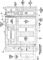
- FIG. 1 is a block diagram representation of an example cellular modem system (modem system) 100.
- Modem system 100 includes a printed circuit board (PCB) 105.
- PCB printed circuit board
- the DC power source 160 may also comprise a single battery, a fuel cell, or a solar cell. DC power source 160 always has current flowing in the same direction between its two terminals.
- a "supercapacitor” (sometimes also referred to as an ultracapacitor, previously an electric double-layer capacitor (EDLC)) is a high-capacity electrochemical capacitor that instead of storing electrical charge directly in dielectric materials as with conventional capacitors, use electrolyte ions which create charge storage in electrical double layers.
- a supercapacitor provides high-capacity with capacitance values much higher than other capacitors (but generally lower voltage limits), which typically store 10 to 100 times more energy per unit volume or mass compared to electrolytic capacitors.
- Supercapacitors are available commercially, such as the HLC-1550 from Tadiran Batteries North New Hyde Park, NY.
- Modem system 100 includes a DC-to-DC converter 115 having inputs coupled to the electrodes 110a, 110b of the capacitor 110.
- the cellular modem 130 is coupled to receive power from an output of the DC-to-DC converter 115 and is coupled to an antenna 135 through an ISW barrier circuit 138 (e.g., DC blocking capacitors).
- the cellular modem 130 may be a Multi-band UMTS/HSPA and CDMA/1XRTT digital cellular radio, Cellular packet switched (IP) connectivity, supports operation with static or dynamic IP addresses, DES-based encryption for secure IP access; Over-the-air (OTA) download of operating system and configuration provides future-proofing, programmable interval sizes: 1, 5, 15, 30, 60 min.
- IP Cellular packet switched
- OTA Over-the-air
- a second IS barrier circuit 120 (e.g., infallible resistors, Zener diodes, and/or active barriers) functioning as a SIM interface circuit is coupled to an output of the cellular modem 130.
- Active barriers include transistors and/or amplifiers (e.g., op amps).
- Infallible resistors are film type resistors, so that they are generally able to withstand at least 1.5x of worst case fault power.
- a film resistor as used herein is its conventional meaning referring to different film types such as carbon film, metal film, and metal oxide film resistors.
- Film resistors are generally manufactured by depositing pure metals (e.g., nickel) or oxide film (e.g., tin-oxide) onto an insulating ceramic or substrate, so that the conductive material does not contain binders or insulating material. This design makes film resistors qualified as infallible resistors.
- pure metals e.g., nickel
- oxide film e.g., tin-oxide
- System 100 includes a microcontroller control section 150 including a microcontroller 140 coupled to a boost regulator 145 having an output coupled to the electrodes 110a, 110b of the capacitor 110.
- the microcontroller 140 is coupled to electrode 110a of the capacitor 110 to receive protected power through R2.
- a metrology jumper 165 is coupled between the microcontroller 140 and a ground of the system through an infallible resistor 167.
- the function of the metrology jumper 165 is to enable changing the metrology related configuration parameters, where the microcontroller 140 senses a break of a shorting bar across the metrology jumper 165 by breaking its seal (as described below) and then removing the short across the metrology jumper terminals.
- the IO connectors 146 are coupled to the modem 130.
- the IO connectors 146 can include an IO pin for receiving data signals, a first SIM reset (RST) pin, core power supply (VCC) pin, a clock (CLK) pin, a battery power supply (VBAT) pin, and SIM side pins including at least a VCC pin, a SIM CLK pin, second SIM RST pin, and a SIM IO pin, as well as and a ground (GND) pin.
- An encapsulation material 142 (such as an epoxy) is for providing a potted area of the PCB potting the capacitor 110, the DC-to-DC converter 115, the cellular modem 130, the second IS barrier circuit 120 and the microcontroller control section 150 including over the PCB 105 in those sections of the board area.
- the encapsulation material 142 allows the modem system 100 to meet the Intrinsic Safe Zone 0 requirement.
- SIM Subscriber Identity Module
- a Subscriber Identity Module (SIM) card 125 inserted into a SIM card connector 126 is coupled to the cellular modem 130 by the second IS barrier circuit 120.
- At least one LED 155 is coupled to the microcontroller 140 through at least one infallible resistor 175. The LED is used for trouble shooting and indicating the health of cellular modem 130.
- the SIM card 125 and LED 155 are in a non-potted area 148 of the PCB.
- a visible light transparent SIM card access cover (transparent cover) 152 is over the SIM card 125 and over the LED 155 having a hinge pivoted to the encapsulation separator 116 for lifting the transparent cover 152 to expose the SIM card 125 for providing access thereto, such as for replacing the SIM card, changing cellular service provider, or obtaining the SIM ICCID number.
- the encapsulation separator 216 comprises a material that is different from the encapsulation material 142, such as polycarbonate.
- FIG. 2 is a depiction of an example packaged cellular modem system (modem system) 200.
- Modem system 200 is designed for an intrinsic safe environment and includes a case 201, connector cover 320, encapsulation separator 116, and a transparent cover 152 over the SIM card 125 and the LED 155.
- the encapsulation separator 116 functions as separator/barrier for the encapsulation material 142 during filling of the encapsulation material to prevent the non-potted area 148 corresponding to the PCB board area of the SIM card 125 and LEDs 155 from receiving encapsulation material 142.
- modem system 200 provides convenient access to the SIM card 125 and SIM card connector 126 and IO connectors 146 shown as RS232/485 connectors, and convenient restricted access to the metrology jumper 165.
- the connector cover is shown as 320, battery 207, external power connection as 208, Jumper RS232/485 209 (for the customer to select between RS232 and RS 485 functionality) with its jumper cover there over, CMOS circuits (as a communication interface), a jumper is 212 (as a power switch; turned on during install), and antenna is 135.
- a pulse input is 214, diversity antenna (antenna div) is 215, and an encapsulation separator 116 separates the potting and non-potting area of PCB 105.
- FIGs. 3A-C show access features of a disclosed metrology jumper 205.
- the metrological jumper 205 access is for configuration without disassembling the electronics assembly from the enclosure.
- the metrology jumper 165 having a jumper cover 166 thereon is placed at an accessible side of the enclosure so that it is accessible for configuration by breaking the metrology seals (see metrology seals 311 and 312 in FIG. 4A and FIG. 6 described below) and removing the connector cover 320 since in the connector cover 320 an inbuilt feature 315 is provided such that it cannot be accessible when connector cover 320is assembled with the case and is sealed by the metrology authority.
- the inbuilt feature 315 in the connector cover 306 restricts access to metrology jumper 165.
- the connector cover 320 can thus be removed by breaking the metrology seals 311, 312.
- FIG. 3B shows the connector cover 320can be removed by breaking the metrology seals 311, 312 on the connector.
- FIG. 3C after the connector cover 206 is removed by breaking the metrology seal 311, 312 on connector and removing then jumper cover 166 the metrology jumper 165 is now accessible (for enabling the removing the shorting bar to allow configuration after removal).
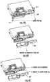
- FIG. 4A-C show metrology jumper access including connector cover 320 removal for a disclosed cellular modem system.
- FIG. 4A shows the seals 311 and 312 that will be broken.
- FIG. 4B shows removal of the connector cover 320 that is enabled by breaking the seals 311 and 312 shown in FIG. 4A .
- FIG. 4C after removing the jumper cover 166, the metrology jumper 165 becomes accessible.
- FIG. 5 shows an encapsulation/potted section view of a disclosed cellular modem system.
- Encapsulation material 142 is provided in the potted area to meet the IS requirement.
- the SIM card connector 126 and LEDs 155 are shown in the non-potted area 148 to allow easy access to the SIM card (after it is seated in the SIM card connector 126) and for the LEDs 155 to be visible to show the health of modem and for a diagnostic purpose.
- FIG. 6 shows all IO connectors 146 on one side of a cellular modem system. All IO connectors 146 are provided on one side of the cellular modem system for easy cable connection and accessibility.
- Benefits of disclosed cellular modem systems include the SIM card 125 can be changed without opening the enclosure. Ease of operation and connectivity for the metrology jumper. All IO connectors 146 being on one side make it convenient to make IO connections. The visible LEDs 155 allows a user to know health of the modem device and for trouble shooting.
- Disclosed embodiments can be applied to generally to any industrial cellular modem.
- an industrial modem in wireless communications with a gas meter that provide synchronized gas day meter reading and interval data to meter data management systems and AutoSol Enterprise Server (AES).
- AES AutoSol Enterprise Server
Landscapes
- Engineering & Computer Science (AREA)
- Computer Networks & Wireless Communication (AREA)
- Signal Processing (AREA)
- Telephonic Communication Services (AREA)
- Telephone Set Structure (AREA)
Description
- Disclosed embodiments relate to packaged intrinsic safe industrial modems.
- A modulator-demodulator (modem) is a hardware device including a transceiver which modulates one or more carrier wave signals to encode digital information for transmission and demodulates modulated signals to decode transmitted information. A modem produces a signal that can be transmitted easily and decoded to reproduce the original digital data. Modems can be used with a variety of transmitters of analog signals, such as a cellular radio. A common type of modem converts the digital data of a computer into modulated electrical signal for transmission over telephone lines and demodulated by another modem at the receiver side to recover the digital data.
- Modems can be used in one wireless modem application to synchronize gas meter reading and interval data to meter data management systems and AutoSol Enterprise Server (AES) software. It can also add significant value to those involved in energy measurement for billing, trading, load management, distribution engineering and custody transfer.
- An industrial modem for the gas industry may comprise a multi-band LTE, UMTS/HSPA and CDMA/1XRTT digital cellular radio, cellular packet switched (IP) connectivity providing the lowest current cost communications available. Such industrial modems support operation with static or dynamic IP addresses, DES based encryption for secure IP access, over-the-air (OTA) download of operating system and configuration provides future-proofing, and programmable interval sizes: 1, 5, 15, 30, 60 min. Depending on data input configuration user defined digital outputs maybe available to provide pulse outputs or control signals to customers. The industrial modem includes a Subscriber Identity Module (SIM) card, where the electronics assembly is potted by an encapsulation material (an epoxy) to meet an Intrinsic Safe Zone 0 safety requirement.
-
US 2009/143111 A1 discloses a portable radio and battery pack configuration. -
US 2015/366084 A1 discloses an intrinsic safe in-line adaptor with an integrated capacitive barrier for connecting a wireless module with an antenna. - The invention is defined by a packaged cellular modem system according to independent claim 1. Embodiments are described by the dependent claims.
-
-
FIG. 1 is a block diagram representation of an example model PCB assembly for a cellular modem system, according to an example embodiment. -
FIG. 2 is depiction of an example packaged cellular modem system, according to an example embodiment. -
FIG. 3A-C show access features of a disclosed metrology jumper, according to an example embodiment. -
FIG. 4A-C show metrology jumper access including connector cover removal for a disclosed cellular modem system. -
FIG. 5 shows an encapsulation/potted section view of a disclosed cellular modem system in which SIM card holder and LED's are not potted. -
FIG. 6 shows all IO connectors on one side of a cellular modem system. - Disclosed embodiments are described with reference to the attached figures, wherein like reference numerals are used throughout the figures to designate similar or equivalent elements. The figures are not drawn to scale and they are provided merely to illustrate certain disclosed aspects. Several disclosed aspects are described below with reference to example applications for illustration. It should be understood that numerous specific details, relationships, and methods are set forth to provide a full understanding of the disclosed embodiments.
- One having ordinary skill in the relevant art, however, will readily recognize that the subject matter disclosed herein can be practiced without one or more of the specific details or with other methods. In other instances, well-known structures or operations are not shown in detail to avoid obscuring certain aspects.
- Also, the terms "coupled to" or "couples with" (and the like) as used herein without further qualification are intended to describe either an indirect or direct electrical connection. Thus, if a first device "couples" to a second device, that connection can be through a direct electrical connection where there are only parasitics in the pathway, or through an indirect electrical connection via intervening items including other devices and connections. For indirect coupling, the intervening item generally does not modify the information of a signal but may adjust its current level, voltage level, and/or power level.
-
FIG. 1 is a block diagram representation of an example cellular modem system (modem system) 100.Modem system 100 includes a printed circuit board (PCB) 105. There is at least one capacitor 110 (e.g. a supercapacitor) havingelectrodes DC power source 160, such as the battery pack shown. TheDC power source 160 may also comprise a single battery, a fuel cell, or a solar cell.DC power source 160 always has current flowing in the same direction between its two terminals. - As used herein, a "supercapacitor" (sometimes also referred to as an ultracapacitor, previously an electric double-layer capacitor (EDLC)) is a high-capacity electrochemical capacitor that instead of storing electrical charge directly in dielectric materials as with conventional capacitors, use electrolyte ions which create charge storage in electrical double layers. A supercapacitor provides high-capacity with capacitance values much higher than other capacitors (but generally lower voltage limits), which typically store 10 to 100 times more energy per unit volume or mass compared to electrolytic capacitors. Supercapacitors are available commercially, such as the HLC-1550 from Tadiran Batteries North New Hyde Park, NY.
-
Modem system 100 includes a DC-to-DC converter 115 having inputs coupled to theelectrodes capacitor 110. Thecellular modem 130 is coupled to receive power from an output of the DC-to-DC converter 115 and is coupled to anantenna 135 through an ISW barrier circuit 138 (e.g., DC blocking capacitors). Thecellular modem 130 may be a Multi-band UMTS/HSPA and CDMA/1XRTT digital cellular radio, Cellular packet switched (IP) connectivity, supports operation with static or dynamic IP addresses, DES-based encryption for secure IP access; Over-the-air (OTA) download of operating system and configuration provides future-proofing, programmable interval sizes: 1, 5, 15, 30, 60 min. Depending on data input configuration user defined digital outputs maybe available to provide pulse outputs or control signals to customers. For gas meter applications for connectivity and communication the modem with SIM interface are needed to connect the gas meter and transfer data to data center for billing and custody transfer. - A second IS barrier circuit 120 (e.g., infallible resistors, Zener diodes, and/or active barriers) functioning as a SIM interface circuit is coupled to an output of the
cellular modem 130. Active barriers include transistors and/or amplifiers (e.g., op amps). Infallible resistors are film type resistors, so that they are generally able to withstand at least 1.5x of worst case fault power. A film resistor as used herein is its conventional meaning referring to different film types such as carbon film, metal film, and metal oxide film resistors. Film resistors are generally manufactured by depositing pure metals (e.g., nickel) or oxide film (e.g., tin-oxide) onto an insulating ceramic or substrate, so that the conductive material does not contain binders or insulating material. This design makes film resistors qualified as infallible resistors. -
System 100 includes amicrocontroller control section 150 including amicrocontroller 140 coupled to aboost regulator 145 having an output coupled to theelectrodes capacitor 110. Themicrocontroller 140 is coupled toelectrode 110a of thecapacitor 110 to receive protected power through R2. Ametrology jumper 165 is coupled between themicrocontroller 140 and a ground of the system through aninfallible resistor 167. The function of themetrology jumper 165 is to enable changing the metrology related configuration parameters, where themicrocontroller 140 senses a break of a shorting bar across themetrology jumper 165 by breaking its seal (as described below) and then removing the short across the metrology jumper terminals. - Input/output (IO)
connectors 146 are coupled to themodem 130. TheIO connectors 146 can include an IO pin for receiving data signals, a first SIM reset (RST) pin, core power supply (VCC) pin, a clock (CLK) pin, a battery power supply (VBAT) pin, and SIM side pins including at least a VCC pin, a SIM CLK pin, second SIM RST pin, and a SIM IO pin, as well as and a ground (GND) pin. An encapsulation material 142 (such as an epoxy) is for providing a potted area of the PCB potting thecapacitor 110, the DC-to-DC converter 115, thecellular modem 130, the secondIS barrier circuit 120 and themicrocontroller control section 150 including over thePCB 105 in those sections of the board area. Theencapsulation material 142 allows themodem system 100 to meet the Intrinsic Safe Zone 0 requirement. - A Subscriber Identity Module (SIM)
card 125 inserted into aSIM card connector 126 is coupled to thecellular modem 130 by the secondIS barrier circuit 120. At least oneLED 155 is coupled to themicrocontroller 140 through at least oneinfallible resistor 175. The LED is used for trouble shooting and indicating the health ofcellular modem 130. TheSIM card 125 andLED 155 are in anon-potted area 148 of the PCB. Instead, a visible light transparent SIM card access cover (transparent cover) 152 is over theSIM card 125 and over theLED 155 having a hinge pivoted to theencapsulation separator 116 for lifting thetransparent cover 152 to expose theSIM card 125 for providing access thereto, such as for replacing the SIM card, changing cellular service provider, or obtaining the SIM ICCID number. The encapsulation separator 216 comprises a material that is different from theencapsulation material 142, such as polycarbonate. -
FIG. 2 is a depiction of an example packaged cellular modem system (modem system) 200.Modem system 200 is designed for an intrinsic safe environment and includes acase 201,connector cover 320,encapsulation separator 116, and atransparent cover 152 over theSIM card 125 and theLED 155. Theencapsulation separator 116 functions as separator/barrier for theencapsulation material 142 during filling of the encapsulation material to prevent thenon-potted area 148 corresponding to the PCB board area of theSIM card 125 andLEDs 155 from receivingencapsulation material 142. As withmodem system 100,modem system 200 provides convenient access to theSIM card 125 andSIM card connector 126 andIO connectors 146 shown as RS232/485 connectors, and convenient restricted access to themetrology jumper 165. The connector cover is shown as 320,battery 207, external power connection as 208, Jumper RS232/485 209 (for the customer to select between RS232 and RS 485 functionality) with its jumper cover there over, CMOS circuits (as a communication interface), a jumper is 212 (as a power switch; turned on during install), and antenna is 135. A pulse input is 214, diversity antenna (antenna div) is 215, and anencapsulation separator 116 separates the potting and non-potting area ofPCB 105. -
FIGs. 3A-C show access features of a disclosed metrology jumper 205. The metrological jumper 205 access is for configuration without disassembling the electronics assembly from the enclosure. Themetrology jumper 165 having ajumper cover 166 thereon is placed at an accessible side of the enclosure so that it is accessible for configuration by breaking the metrology seals (seemetrology seals FIG. 4A andFIG. 6 described below) and removing theconnector cover 320 since in theconnector cover 320 aninbuilt feature 315 is provided such that it cannot be accessible when connector cover 320is assembled with the case and is sealed by the metrology authority. As shown inFIG. 3A , theinbuilt feature 315 in the connector cover 306restricts access tometrology jumper 165. Theconnector cover 320 can thus be removed by breaking the metrology seals 311, 312.FIG. 3B shows the connector cover 320can be removed by breaking the metrology seals 311, 312 on the connector. As shown inFIG. 3C , after the connector cover 206 is removed by breaking themetrology seal jumper cover 166 themetrology jumper 165 is now accessible (for enabling the removing the shorting bar to allow configuration after removal). -
FIG. 4A-C show metrology jumper access includingconnector cover 320 removal for a disclosed cellular modem system.FIG. 4A shows theseals FIG. 4B shows removal of theconnector cover 320 that is enabled by breaking theseals FIG. 4A . As shown inFIG. 4C , after removing thejumper cover 166, themetrology jumper 165 becomes accessible. -
FIG. 5 shows an encapsulation/potted section view of a disclosed cellular modem system.Encapsulation material 142 is provided in the potted area to meet the IS requirement. TheSIM card connector 126 andLEDs 155 are shown in thenon-potted area 148 to allow easy access to the SIM card (after it is seated in the SIM card connector 126) and for theLEDs 155 to be visible to show the health of modem and for a diagnostic purpose.FIG. 6 shows allIO connectors 146 on one side of a cellular modem system. AllIO connectors 146 are provided on one side of the cellular modem system for easy cable connection and accessibility. - Benefits of disclosed cellular modem systems include the
SIM card 125 can be changed without opening the enclosure. Ease of operation and connectivity for the metrology jumper. AllIO connectors 146 being on one side make it convenient to make IO connections. Thevisible LEDs 155 allows a user to know health of the modem device and for trouble shooting. - Disclosed embodiments can be applied to generally to any industrial cellular modem. For example, as an industrial modem in wireless communications with a gas meter that provide synchronized gas day meter reading and interval data to meter data management systems and AutoSol Enterprise Server (AES).
- While various disclosed embodiments have been described above, it should be understood that they have been presented by way of example only, and not limitation. Numerous changes to the subject matter disclosed herein can be made in accordance with this Disclosure without departing from the scope of the appended claims.
Claims (6)
- A packaged cellular modem system (100), comprising:a printed circuit board (105) upon which said modem system is configured;at least one capacitor (110) having electrodes (110a), (110b) coupled for receiving power from a DC power source (160),a DC-to-DC converter (115) having inputs coupled to said electrodes (110a), (110b),a cellular modem (130) coupled to an output of said DC-to-DC converter (115),an antenna (135) coupled to the said cellular modem through a first intrinsic safety barrier circuit (138),a second intrinsic safety barrier circuit (120) coupled to an output of said cellular modem (130);a microcontroller control section (150) including a microcontroller (140) coupled to a boost regulator (145) having an output coupled to said electrodes (110a), (110b) for receiving power, and a metrology jumper (165) coupled between said microcontroller and a ground pin;input/output connectors (146) coupled to said cellular modem;an encapsulation material (142) providing a potted area of said printed circuit board which is configured to pot said capacitor (110), said DC-to-DC converter (115), said cellular modem (130), said second intrinsic safety barrier circuit (120), and said microcontroller control section (150);a Subscriber Identity Module card (125) inserted into a Subscriber Identity Module connector (126), the Subscriber Identity Module connector being coupled to said cellular modem (110) by said second intrinsic safety barrier circuit (120);light emitting diodes (155) coupled to said microcontroller (140),wherein said Subscriber Identity Module card and said light emitting diodes are in a non-potted area (148) of said printed circuit board;a visible light transparent Subscriber Identity Module card access cover (152) being configured over said Subscriber Identity Module card (125) and over said light emitting diodes (155); the visible light transparent Subscriber Identity Module card access cover (152) having a hinge pivoted to an encapsulation separator (116) for lifting said visible light transparent Subscriber Identity Module card access cover (152) to expose said Subscriber Identity Module card for providing access thereto.
- The modem system of claim 1, wherein said capacitor (110) comprises a supercapacitor.
- The modem system of claim 1, wherein all said input/output connectors (146) are located on one side of said modem system.
- The modem system of claim 1, said metrology jumper (165) being accessible for configuration by breaking a metrology seal and removing a connector cover that is over said metrology jumper (165).
- The modem system of claim 1, further comprising an outer case (201) having a cutout which is configured to expose said non-potted area of said printed circuit board.
- The modem system of claim 5, further comprising a connector cover (320) secured to said outer case (201) by metrology seals (311), (312), wherein said connector cover (320) is removable by breaking said metrology seals.
Applications Claiming Priority (1)
| Application Number | Priority Date | Filing Date | Title |
|---|---|---|---|
| US15/060,201 US9948337B2 (en) | 2016-03-03 | 2016-03-03 | Packaged intrinsic safe industrial modem |
Publications (2)
| Publication Number | Publication Date |
|---|---|
| EP3214714A1 EP3214714A1 (en) | 2017-09-06 |
| EP3214714B1 true EP3214714B1 (en) | 2021-09-15 |
Family
ID=58158780
Family Applications (1)
| Application Number | Title | Priority Date | Filing Date |
|---|---|---|---|
| EP17154895.1A Active EP3214714B1 (en) | 2016-03-03 | 2017-02-06 | Packaged intrinsic safe industrial modem |
Country Status (2)
| Country | Link |
|---|---|
| US (1) | US9948337B2 (en) |
| EP (1) | EP3214714B1 (en) |
Families Citing this family (2)
| Publication number | Priority date | Publication date | Assignee | Title |
|---|---|---|---|---|
| WO2020049744A1 (en) | 2018-09-07 | 2020-03-12 | Smc株式会社 | Wireless antenna module and wireless system |
| US12627364B2 (en) * | 2021-08-23 | 2026-05-12 | Napco Security Technologies, Inc. | Security communicator dual antenna system |
Family Cites Families (14)
| Publication number | Priority date | Publication date | Assignee | Title |
|---|---|---|---|---|
| US3969143A (en) | 1975-07-22 | 1976-07-13 | Wilson Greatbatch Ltd. | Enclosure for lithium-iodine cell and method of making the same |
| CN1196361C (en) * | 2001-05-04 | 2005-04-06 | Lg电子株式会社 | Device and method of verifying subscriber identifying module card |
| US7868903B2 (en) | 2004-10-14 | 2011-01-11 | Daktronics, Inc. | Flexible pixel element fabrication and sealing method |
| US7945295B2 (en) * | 2007-12-03 | 2011-05-17 | Motorola Solutions, Inc. | Portable radio and battery pack configuration |
| US8185101B1 (en) | 2008-04-10 | 2012-05-22 | Sandia Corporation | Handheld portable real-time tracking and communications device |
| US8125785B2 (en) | 2008-06-11 | 2012-02-28 | Adc Telecommunications, Inc. | Angled doors with continuous seal |
| US8544755B2 (en) * | 2010-06-28 | 2013-10-01 | United Test And Assembly Center Ltd. | Subscriber identity module (SIM) card |
| US8674539B1 (en) * | 2010-10-01 | 2014-03-18 | Qualcomm Incorporated | Powerline communication power supply and modem interface mechanism |
| GB201116883D0 (en) | 2011-09-30 | 2011-11-16 | Johnson Matthey Plc | Radiation detector |
| US20140200047A1 (en) * | 2013-01-11 | 2014-07-17 | Kuo-Liang Chen | Interface Card with Multiple Subscriber Identity Modules |
| US9059538B2 (en) | 2013-03-14 | 2015-06-16 | Itron, Inc. | Electrical conductor assembly for intra-enclosure conductor termination |
| GB2517776B (en) * | 2013-08-30 | 2016-05-11 | Cylon Global Technology Inc | Power supply circuit for mobile telecommunications devices |
| US9680261B2 (en) * | 2014-06-11 | 2017-06-13 | Honewell International Inc. | Intrinsic safe in-line adaptor with integrated capacitive barrier for connecting a wireless module with antenna |
| US9374255B1 (en) * | 2015-06-16 | 2016-06-21 | Honeywell International Inc. | Interface circuit for providing high speed digital communication between a master universal asynchronous receiver transmitter (UART) device and a 1-wire, UART compatible sensor |
-
2016
- 2016-03-03 US US15/060,201 patent/US9948337B2/en active Active
-
2017
- 2017-02-06 EP EP17154895.1A patent/EP3214714B1/en active Active
Also Published As
| Publication number | Publication date |
|---|---|
| EP3214714A1 (en) | 2017-09-06 |
| US20170257130A1 (en) | 2017-09-07 |
| US9948337B2 (en) | 2018-04-17 |
Similar Documents
| Publication | Publication Date | Title |
|---|---|---|
| US20150372516A1 (en) | Identification module card including battery protection circuit module, and portable wireless device including the identification module card | |
| US20170163062A9 (en) | Wearable / mountable mobile charging device | |
| CN107851859A (en) | Include the battery of battery mo(u)ld top half indicator | |
| WO2008002487A8 (en) | Integrated current-interrupt device for lithium-ion cells | |
| CN107006124A (en) | Surface mount batteries and portable electronic devices with integrated battery cells | |
| CN105580163A (en) | Battery pack having PCM case | |
| CN105556708A (en) | Battery pack with protective circuit module securing tape | |
| CN101944752A (en) | Power supply device | |
| WO2015191577A1 (en) | Modularized communication device | |
| US9948337B2 (en) | Packaged intrinsic safe industrial modem | |
| US8491329B2 (en) | Electrical outlet assembly and manufacturing method thereof | |
| US20140211773A1 (en) | Vehicle wireless router | |
| US20140323042A1 (en) | Watch with wireless communication functionality | |
| US20190081362A1 (en) | Over-Molded Printed Circuit Board Connector | |
| CN205206509U (en) | Electronic lock with emergent power supply interface | |
| CN210627187U (en) | Multifunctional storage device | |
| CN104283416A (en) | Self-adaptation power supply system and power supply method thereof | |
| EP3217500A1 (en) | Interface device providing intrinsic safety for a communications device | |
| CN204067630U (en) | A kind of electronic equipment charging base | |
| CN202929393U (en) | GSM communication circuit based on intelligent household control | |
| KR101800814B1 (en) | Battery pack having an USB charger terminal | |
| CN208209194U (en) | A kind of multifunction combined external plug and Multifunctional data line | |
| CN106713564B (en) | A kind of multifunction intelligent mobile telephone shell | |
| KR20130119746A (en) | Power supply device based on device id recognition | |
| CN205646038U (en) | Battery module and unmanned aircraft with high-precision digital capacity display |
Legal Events
| Date | Code | Title | Description |
|---|---|---|---|
| PUAI | Public reference made under article 153(3) epc to a published international application that has entered the european phase |
Free format text: ORIGINAL CODE: 0009012 |
|
| STAA | Information on the status of an ep patent application or granted ep patent |
Free format text: STATUS: REQUEST FOR EXAMINATION WAS MADE |
|
| 17P | Request for examination filed |
Effective date: 20170206 |
|
| AK | Designated contracting states |
Kind code of ref document: A1 Designated state(s): AL AT BE BG CH CY CZ DE DK EE ES FI FR GB GR HR HU IE IS IT LI LT LU LV MC MK MT NL NO PL PT RO RS SE SI SK SM TR |
|
| AX | Request for extension of the european patent |
Extension state: BA ME |
|
| REG | Reference to a national code |
Ref country code: DE Ref legal event code: R079 Ref document number: 602017045931 Country of ref document: DE Free format text: PREVIOUS MAIN CLASS: H02H0009000000 Ipc: H04B0001381800 |
|
| GRAP | Despatch of communication of intention to grant a patent |
Free format text: ORIGINAL CODE: EPIDOSNIGR1 |
|
| STAA | Information on the status of an ep patent application or granted ep patent |
Free format text: STATUS: GRANT OF PATENT IS INTENDED |
|
| RIC1 | Information provided on ipc code assigned before grant |
Ipc: H04B 1/3818 20150101AFI20210319BHEP |
|
| INTG | Intention to grant announced |
Effective date: 20210414 |
|
| GRAS | Grant fee paid |
Free format text: ORIGINAL CODE: EPIDOSNIGR3 |
|
| GRAA | (expected) grant |
Free format text: ORIGINAL CODE: 0009210 |
|
| STAA | Information on the status of an ep patent application or granted ep patent |
Free format text: STATUS: THE PATENT HAS BEEN GRANTED |
|
| AK | Designated contracting states |
Kind code of ref document: B1 Designated state(s): AL AT BE BG CH CY CZ DE DK EE ES FI FR GB GR HR HU IE IS IT LI LT LU LV MC MK MT NL NO PL PT RO RS SE SI SK SM TR |
|
| REG | Reference to a national code |
Ref country code: CH Ref legal event code: EP |
|
| REG | Reference to a national code |
Ref country code: DE Ref legal event code: R096 Ref document number: 602017045931 Country of ref document: DE |
|
| REG | Reference to a national code |
Ref country code: IE Ref legal event code: FG4D |
|
| REG | Reference to a national code |
Ref country code: AT Ref legal event code: REF Ref document number: 1431337 Country of ref document: AT Kind code of ref document: T Effective date: 20211015 |
|
| REG | Reference to a national code |
Ref country code: NL Ref legal event code: FP |
|
| REG | Reference to a national code |
Ref country code: LT Ref legal event code: MG9D |
|
| PG25 | Lapsed in a contracting state [announced via postgrant information from national office to epo] |
Ref country code: RS Free format text: LAPSE BECAUSE OF FAILURE TO SUBMIT A TRANSLATION OF THE DESCRIPTION OR TO PAY THE FEE WITHIN THE PRESCRIBED TIME-LIMIT Effective date: 20210915 Ref country code: SE Free format text: LAPSE BECAUSE OF FAILURE TO SUBMIT A TRANSLATION OF THE DESCRIPTION OR TO PAY THE FEE WITHIN THE PRESCRIBED TIME-LIMIT Effective date: 20210915 Ref country code: BG Free format text: LAPSE BECAUSE OF FAILURE TO SUBMIT A TRANSLATION OF THE DESCRIPTION OR TO PAY THE FEE WITHIN THE PRESCRIBED TIME-LIMIT Effective date: 20211215 Ref country code: LT Free format text: LAPSE BECAUSE OF FAILURE TO SUBMIT A TRANSLATION OF THE DESCRIPTION OR TO PAY THE FEE WITHIN THE PRESCRIBED TIME-LIMIT Effective date: 20210915 Ref country code: NO Free format text: LAPSE BECAUSE OF FAILURE TO SUBMIT A TRANSLATION OF THE DESCRIPTION OR TO PAY THE FEE WITHIN THE PRESCRIBED TIME-LIMIT Effective date: 20211215 Ref country code: FI Free format text: LAPSE BECAUSE OF FAILURE TO SUBMIT A TRANSLATION OF THE DESCRIPTION OR TO PAY THE FEE WITHIN THE PRESCRIBED TIME-LIMIT Effective date: 20210915 Ref country code: HR Free format text: LAPSE BECAUSE OF FAILURE TO SUBMIT A TRANSLATION OF THE DESCRIPTION OR TO PAY THE FEE WITHIN THE PRESCRIBED TIME-LIMIT Effective date: 20210915 |
|
| REG | Reference to a national code |
Ref country code: AT Ref legal event code: MK05 Ref document number: 1431337 Country of ref document: AT Kind code of ref document: T Effective date: 20210915 |
|
| PG25 | Lapsed in a contracting state [announced via postgrant information from national office to epo] |
Ref country code: LV Free format text: LAPSE BECAUSE OF FAILURE TO SUBMIT A TRANSLATION OF THE DESCRIPTION OR TO PAY THE FEE WITHIN THE PRESCRIBED TIME-LIMIT Effective date: 20210915 Ref country code: GR Free format text: LAPSE BECAUSE OF FAILURE TO SUBMIT A TRANSLATION OF THE DESCRIPTION OR TO PAY THE FEE WITHIN THE PRESCRIBED TIME-LIMIT Effective date: 20211216 |
|
| PG25 | Lapsed in a contracting state [announced via postgrant information from national office to epo] |
Ref country code: AT Free format text: LAPSE BECAUSE OF FAILURE TO SUBMIT A TRANSLATION OF THE DESCRIPTION OR TO PAY THE FEE WITHIN THE PRESCRIBED TIME-LIMIT Effective date: 20210915 |
|
| PG25 | Lapsed in a contracting state [announced via postgrant information from national office to epo] |
Ref country code: IS Free format text: LAPSE BECAUSE OF FAILURE TO SUBMIT A TRANSLATION OF THE DESCRIPTION OR TO PAY THE FEE WITHIN THE PRESCRIBED TIME-LIMIT Effective date: 20220115 Ref country code: SM Free format text: LAPSE BECAUSE OF FAILURE TO SUBMIT A TRANSLATION OF THE DESCRIPTION OR TO PAY THE FEE WITHIN THE PRESCRIBED TIME-LIMIT Effective date: 20210915 Ref country code: SK Free format text: LAPSE BECAUSE OF FAILURE TO SUBMIT A TRANSLATION OF THE DESCRIPTION OR TO PAY THE FEE WITHIN THE PRESCRIBED TIME-LIMIT Effective date: 20210915 Ref country code: RO Free format text: LAPSE BECAUSE OF FAILURE TO SUBMIT A TRANSLATION OF THE DESCRIPTION OR TO PAY THE FEE WITHIN THE PRESCRIBED TIME-LIMIT Effective date: 20210915 Ref country code: PT Free format text: LAPSE BECAUSE OF FAILURE TO SUBMIT A TRANSLATION OF THE DESCRIPTION OR TO PAY THE FEE WITHIN THE PRESCRIBED TIME-LIMIT Effective date: 20220117 Ref country code: PL Free format text: LAPSE BECAUSE OF FAILURE TO SUBMIT A TRANSLATION OF THE DESCRIPTION OR TO PAY THE FEE WITHIN THE PRESCRIBED TIME-LIMIT Effective date: 20210915 Ref country code: ES Free format text: LAPSE BECAUSE OF FAILURE TO SUBMIT A TRANSLATION OF THE DESCRIPTION OR TO PAY THE FEE WITHIN THE PRESCRIBED TIME-LIMIT Effective date: 20210915 Ref country code: EE Free format text: LAPSE BECAUSE OF FAILURE TO SUBMIT A TRANSLATION OF THE DESCRIPTION OR TO PAY THE FEE WITHIN THE PRESCRIBED TIME-LIMIT Effective date: 20210915 Ref country code: CZ Free format text: LAPSE BECAUSE OF FAILURE TO SUBMIT A TRANSLATION OF THE DESCRIPTION OR TO PAY THE FEE WITHIN THE PRESCRIBED TIME-LIMIT Effective date: 20210915 Ref country code: AL Free format text: LAPSE BECAUSE OF FAILURE TO SUBMIT A TRANSLATION OF THE DESCRIPTION OR TO PAY THE FEE WITHIN THE PRESCRIBED TIME-LIMIT Effective date: 20210915 |
|
| REG | Reference to a national code |
Ref country code: DE Ref legal event code: R097 Ref document number: 602017045931 Country of ref document: DE |
|
| PLBE | No opposition filed within time limit |
Free format text: ORIGINAL CODE: 0009261 |
|
| STAA | Information on the status of an ep patent application or granted ep patent |
Free format text: STATUS: NO OPPOSITION FILED WITHIN TIME LIMIT |
|
| PG25 | Lapsed in a contracting state [announced via postgrant information from national office to epo] |
Ref country code: DK Free format text: LAPSE BECAUSE OF FAILURE TO SUBMIT A TRANSLATION OF THE DESCRIPTION OR TO PAY THE FEE WITHIN THE PRESCRIBED TIME-LIMIT Effective date: 20210915 |
|
| 26N | No opposition filed |
Effective date: 20220616 |
|
| PG25 | Lapsed in a contracting state [announced via postgrant information from national office to epo] |
Ref country code: SI Free format text: LAPSE BECAUSE OF FAILURE TO SUBMIT A TRANSLATION OF THE DESCRIPTION OR TO PAY THE FEE WITHIN THE PRESCRIBED TIME-LIMIT Effective date: 20210915 |
|
| PG25 | Lapsed in a contracting state [announced via postgrant information from national office to epo] |
Ref country code: MC Free format text: LAPSE BECAUSE OF FAILURE TO SUBMIT A TRANSLATION OF THE DESCRIPTION OR TO PAY THE FEE WITHIN THE PRESCRIBED TIME-LIMIT Effective date: 20210915 |
|
| REG | Reference to a national code |
Ref country code: CH Ref legal event code: PL |
|
| REG | Reference to a national code |
Ref country code: BE Ref legal event code: MM Effective date: 20220228 |
|
| PG25 | Lapsed in a contracting state [announced via postgrant information from national office to epo] |
Ref country code: LU Free format text: LAPSE BECAUSE OF NON-PAYMENT OF DUE FEES Effective date: 20220206 |
|
| PG25 | Lapsed in a contracting state [announced via postgrant information from national office to epo] |
Ref country code: LI Free format text: LAPSE BECAUSE OF NON-PAYMENT OF DUE FEES Effective date: 20220228 Ref country code: IT Free format text: LAPSE BECAUSE OF FAILURE TO SUBMIT A TRANSLATION OF THE DESCRIPTION OR TO PAY THE FEE WITHIN THE PRESCRIBED TIME-LIMIT Effective date: 20210915 Ref country code: IE Free format text: LAPSE BECAUSE OF NON-PAYMENT OF DUE FEES Effective date: 20220206 Ref country code: CH Free format text: LAPSE BECAUSE OF NON-PAYMENT OF DUE FEES Effective date: 20220228 |
|
| PG25 | Lapsed in a contracting state [announced via postgrant information from national office to epo] |
Ref country code: BE Free format text: LAPSE BECAUSE OF NON-PAYMENT OF DUE FEES Effective date: 20220228 |
|
| P01 | Opt-out of the competence of the unified patent court (upc) registered |
Effective date: 20230414 |
|
| PG25 | Lapsed in a contracting state [announced via postgrant information from national office to epo] |
Ref country code: HU Free format text: LAPSE BECAUSE OF FAILURE TO SUBMIT A TRANSLATION OF THE DESCRIPTION OR TO PAY THE FEE WITHIN THE PRESCRIBED TIME-LIMIT; INVALID AB INITIO Effective date: 20170206 |
|
| PG25 | Lapsed in a contracting state [announced via postgrant information from national office to epo] |
Ref country code: MK Free format text: LAPSE BECAUSE OF FAILURE TO SUBMIT A TRANSLATION OF THE DESCRIPTION OR TO PAY THE FEE WITHIN THE PRESCRIBED TIME-LIMIT Effective date: 20210915 Ref country code: CY Free format text: LAPSE BECAUSE OF FAILURE TO SUBMIT A TRANSLATION OF THE DESCRIPTION OR TO PAY THE FEE WITHIN THE PRESCRIBED TIME-LIMIT Effective date: 20210915 |
|
| PG25 | Lapsed in a contracting state [announced via postgrant information from national office to epo] |
Ref country code: TR Free format text: LAPSE BECAUSE OF FAILURE TO SUBMIT A TRANSLATION OF THE DESCRIPTION OR TO PAY THE FEE WITHIN THE PRESCRIBED TIME-LIMIT Effective date: 20210915 |
|
| PG25 | Lapsed in a contracting state [announced via postgrant information from national office to epo] |
Ref country code: MT Free format text: LAPSE BECAUSE OF FAILURE TO SUBMIT A TRANSLATION OF THE DESCRIPTION OR TO PAY THE FEE WITHIN THE PRESCRIBED TIME-LIMIT Effective date: 20210915 |
|
| PGFP | Annual fee paid to national office [announced via postgrant information from national office to epo] |
Ref country code: NL Payment date: 20260220 Year of fee payment: 10 |
|
| PGFP | Annual fee paid to national office [announced via postgrant information from national office to epo] |
Ref country code: GB Payment date: 20260223 Year of fee payment: 10 |
|
| PGFP | Annual fee paid to national office [announced via postgrant information from national office to epo] |
Ref country code: DE Payment date: 20260220 Year of fee payment: 10 |
|
| PGFP | Annual fee paid to national office [announced via postgrant information from national office to epo] |
Ref country code: FR Payment date: 20260224 Year of fee payment: 10 |