EP3211669B1 - Semiconductor package with isolation wall - Google Patents
Semiconductor package with isolation wall Download PDFInfo
- Publication number
- EP3211669B1 EP3211669B1 EP17154795.3A EP17154795A EP3211669B1 EP 3211669 B1 EP3211669 B1 EP 3211669B1 EP 17154795 A EP17154795 A EP 17154795A EP 3211669 B1 EP3211669 B1 EP 3211669B1
- Authority
- EP
- European Patent Office
- Prior art keywords
- isolation wall
- lead frame
- indentations
- substrate
- interconnects
- Prior art date
- Legal status (The legal status is an assumption and is not a legal conclusion. Google has not performed a legal analysis and makes no representation as to the accuracy of the status listed.)
- Active
Links
Images


Classifications
-
- H—ELECTRICITY
- H10—SEMICONDUCTOR DEVICES; ELECTRIC SOLID-STATE DEVICES NOT OTHERWISE PROVIDED FOR
- H10W—GENERIC PACKAGES, INTERCONNECTIONS, CONNECTORS OR OTHER CONSTRUCTIONAL DETAILS OF DEVICES COVERED BY CLASS H10
- H10W44/00—Electrical arrangements for controlling or matching impedance
- H10W44/20—Electrical arrangements for controlling or matching impedance at high-frequency [HF] or radio frequency [RF]
-
- H—ELECTRICITY
- H03—ELECTRONIC CIRCUITRY
- H03F—AMPLIFIERS
- H03F1/00—Details of amplifiers with only discharge tubes, only semiconductor devices or only unspecified devices as amplifying elements
- H03F1/02—Modifications of amplifiers to raise the efficiency, e.g. gliding Class A stages, use of an auxiliary oscillation
- H03F1/0205—Modifications of amplifiers to raise the efficiency, e.g. gliding Class A stages, use of an auxiliary oscillation in transistor amplifiers
- H03F1/0288—Modifications of amplifiers to raise the efficiency, e.g. gliding Class A stages, use of an auxiliary oscillation in transistor amplifiers using a main and one or several auxiliary peaking amplifiers whereby the load is connected to the main amplifier using an impedance inverter, e.g. Doherty amplifiers
-
- H—ELECTRICITY
- H03—ELECTRONIC CIRCUITRY
- H03F—AMPLIFIERS
- H03F3/00—Amplifiers with only discharge tubes or only semiconductor devices as amplifying elements
- H03F3/189—High-frequency amplifiers, e.g. radio frequency amplifiers
- H03F3/19—High-frequency amplifiers, e.g. radio frequency amplifiers with semiconductor devices only
- H03F3/195—High-frequency amplifiers, e.g. radio frequency amplifiers with semiconductor devices only in integrated circuits
-
- H—ELECTRICITY
- H03—ELECTRONIC CIRCUITRY
- H03F—AMPLIFIERS
- H03F3/00—Amplifiers with only discharge tubes or only semiconductor devices as amplifying elements
- H03F3/20—Power amplifiers, e.g. Class B amplifiers, Class C amplifiers
- H03F3/21—Power amplifiers, e.g. Class B amplifiers, Class C amplifiers with semiconductor devices only
- H03F3/211—Power amplifiers, e.g. Class B amplifiers, Class C amplifiers with semiconductor devices only using a combination of several amplifiers
-
- H—ELECTRICITY
- H03—ELECTRONIC CIRCUITRY
- H03F—AMPLIFIERS
- H03F3/00—Amplifiers with only discharge tubes or only semiconductor devices as amplifying elements
- H03F3/20—Power amplifiers, e.g. Class B amplifiers, Class C amplifiers
- H03F3/24—Power amplifiers, e.g. Class B amplifiers, Class C amplifiers of transmitter output stages
- H03F3/245—Power amplifiers, e.g. Class B amplifiers, Class C amplifiers of transmitter output stages with semiconductor devices only
-
- H—ELECTRICITY
- H10—SEMICONDUCTOR DEVICES; ELECTRIC SOLID-STATE DEVICES NOT OTHERWISE PROVIDED FOR
- H10D—INORGANIC ELECTRIC SEMICONDUCTOR DEVICES
- H10D64/00—Electrodes of devices having potential barriers
- H10D64/60—Electrodes characterised by their materials
- H10D64/66—Electrodes having a conductor capacitively coupled to a semiconductor by an insulator, e.g. MIS electrodes
-
- H—ELECTRICITY
- H10—SEMICONDUCTOR DEVICES; ELECTRIC SOLID-STATE DEVICES NOT OTHERWISE PROVIDED FOR
- H10W—GENERIC PACKAGES, INTERCONNECTIONS, CONNECTORS OR OTHER CONSTRUCTIONAL DETAILS OF DEVICES COVERED BY CLASS H10
- H10W42/00—Arrangements for protection of devices
- H10W42/20—Arrangements for protection of devices protecting against electromagnetic or particle radiation, e.g. light, X-rays, gamma-rays or electrons
-
- H—ELECTRICITY
- H10—SEMICONDUCTOR DEVICES; ELECTRIC SOLID-STATE DEVICES NOT OTHERWISE PROVIDED FOR
- H10W—GENERIC PACKAGES, INTERCONNECTIONS, CONNECTORS OR OTHER CONSTRUCTIONAL DETAILS OF DEVICES COVERED BY CLASS H10
- H10W42/00—Arrangements for protection of devices
- H10W42/20—Arrangements for protection of devices protecting against electromagnetic or particle radiation, e.g. light, X-rays, gamma-rays or electrons
- H10W42/261—Arrangements for protection of devices protecting against electromagnetic or particle radiation, e.g. light, X-rays, gamma-rays or electrons characterised by their shapes or dispositions
- H10W42/273—Arrangements for protection of devices protecting against electromagnetic or particle radiation, e.g. light, X-rays, gamma-rays or electrons characterised by their shapes or dispositions the arrangements being between laterally adjacent chips, e.g. walls between chips
-
- H—ELECTRICITY
- H10—SEMICONDUCTOR DEVICES; ELECTRIC SOLID-STATE DEVICES NOT OTHERWISE PROVIDED FOR
- H10W—GENERIC PACKAGES, INTERCONNECTIONS, CONNECTORS OR OTHER CONSTRUCTIONAL DETAILS OF DEVICES COVERED BY CLASS H10
- H10W70/00—Package substrates; Interposers; Redistribution layers [RDL]
- H10W70/40—Leadframes
- H10W70/421—Shapes or dispositions
-
- H—ELECTRICITY
- H10—SEMICONDUCTOR DEVICES; ELECTRIC SOLID-STATE DEVICES NOT OTHERWISE PROVIDED FOR
- H10W—GENERIC PACKAGES, INTERCONNECTIONS, CONNECTORS OR OTHER CONSTRUCTIONAL DETAILS OF DEVICES COVERED BY CLASS H10
- H10W70/00—Package substrates; Interposers; Redistribution layers [RDL]
- H10W70/40—Leadframes
- H10W70/421—Shapes or dispositions
- H10W70/424—Cross-sectional shapes
-
- H—ELECTRICITY
- H10—SEMICONDUCTOR DEVICES; ELECTRIC SOLID-STATE DEVICES NOT OTHERWISE PROVIDED FOR
- H10W—GENERIC PACKAGES, INTERCONNECTIONS, CONNECTORS OR OTHER CONSTRUCTIONAL DETAILS OF DEVICES COVERED BY CLASS H10
- H10W70/00—Package substrates; Interposers; Redistribution layers [RDL]
- H10W70/40—Leadframes
- H10W70/421—Shapes or dispositions
- H10W70/424—Cross-sectional shapes
- H10W70/427—Bent parts
-
- H—ELECTRICITY
- H10—SEMICONDUCTOR DEVICES; ELECTRIC SOLID-STATE DEVICES NOT OTHERWISE PROVIDED FOR
- H10W—GENERIC PACKAGES, INTERCONNECTIONS, CONNECTORS OR OTHER CONSTRUCTIONAL DETAILS OF DEVICES COVERED BY CLASS H10
- H10W72/00—Interconnections or connectors in packages
-
- H—ELECTRICITY
- H10—SEMICONDUCTOR DEVICES; ELECTRIC SOLID-STATE DEVICES NOT OTHERWISE PROVIDED FOR
- H10W—GENERIC PACKAGES, INTERCONNECTIONS, CONNECTORS OR OTHER CONSTRUCTIONAL DETAILS OF DEVICES COVERED BY CLASS H10
- H10W74/00—Encapsulations, e.g. protective coatings
- H10W74/01—Manufacture or treatment
-
- H—ELECTRICITY
- H10—SEMICONDUCTOR DEVICES; ELECTRIC SOLID-STATE DEVICES NOT OTHERWISE PROVIDED FOR
- H10W—GENERIC PACKAGES, INTERCONNECTIONS, CONNECTORS OR OTHER CONSTRUCTIONAL DETAILS OF DEVICES COVERED BY CLASS H10
- H10W74/00—Encapsulations, e.g. protective coatings
- H10W74/10—Encapsulations, e.g. protective coatings characterised by their shape or disposition
- H10W74/111—Encapsulations, e.g. protective coatings characterised by their shape or disposition the semiconductor body being completely enclosed
- H10W74/114—Encapsulations, e.g. protective coatings characterised by their shape or disposition the semiconductor body being completely enclosed by a substrate and the encapsulations
-
- H—ELECTRICITY
- H10—SEMICONDUCTOR DEVICES; ELECTRIC SOLID-STATE DEVICES NOT OTHERWISE PROVIDED FOR
- H10W—GENERIC PACKAGES, INTERCONNECTIONS, CONNECTORS OR OTHER CONSTRUCTIONAL DETAILS OF DEVICES COVERED BY CLASS H10
- H10W76/00—Containers; Fillings or auxiliary members therefor; Seals
- H10W76/40—Fillings or auxiliary members in containers, e.g. centering rings
-
- H—ELECTRICITY
- H10—SEMICONDUCTOR DEVICES; ELECTRIC SOLID-STATE DEVICES NOT OTHERWISE PROVIDED FOR
- H10W—GENERIC PACKAGES, INTERCONNECTIONS, CONNECTORS OR OTHER CONSTRUCTIONAL DETAILS OF DEVICES COVERED BY CLASS H10
- H10W90/00—Package configurations
-
- H—ELECTRICITY
- H10—SEMICONDUCTOR DEVICES; ELECTRIC SOLID-STATE DEVICES NOT OTHERWISE PROVIDED FOR
- H10W—GENERIC PACKAGES, INTERCONNECTIONS, CONNECTORS OR OTHER CONSTRUCTIONAL DETAILS OF DEVICES COVERED BY CLASS H10
- H10W90/00—Package configurations
- H10W90/811—Multiple chips on leadframes
-
- H—ELECTRICITY
- H03—ELECTRONIC CIRCUITRY
- H03F—AMPLIFIERS
- H03F2200/00—Indexing scheme relating to amplifiers
- H03F2200/451—Indexing scheme relating to amplifiers the amplifier being a radio frequency amplifier
-
- H—ELECTRICITY
- H10—SEMICONDUCTOR DEVICES; ELECTRIC SOLID-STATE DEVICES NOT OTHERWISE PROVIDED FOR
- H10W—GENERIC PACKAGES, INTERCONNECTIONS, CONNECTORS OR OTHER CONSTRUCTIONAL DETAILS OF DEVICES COVERED BY CLASS H10
- H10W44/00—Electrical arrangements for controlling or matching impedance
- H10W44/20—Electrical arrangements for controlling or matching impedance at high-frequency [HF] or radio frequency [RF]
- H10W44/203—Electrical connections
- H10W44/206—Wires
-
- H—ELECTRICITY
- H10—SEMICONDUCTOR DEVICES; ELECTRIC SOLID-STATE DEVICES NOT OTHERWISE PROVIDED FOR
- H10W—GENERIC PACKAGES, INTERCONNECTIONS, CONNECTORS OR OTHER CONSTRUCTIONAL DETAILS OF DEVICES COVERED BY CLASS H10
- H10W44/00—Electrical arrangements for controlling or matching impedance
- H10W44/20—Electrical arrangements for controlling or matching impedance at high-frequency [HF] or radio frequency [RF]
- H10W44/226—Electrical arrangements for controlling or matching impedance at high-frequency [HF] or radio frequency [RF] for HF amplifiers
-
- H—ELECTRICITY
- H10—SEMICONDUCTOR DEVICES; ELECTRIC SOLID-STATE DEVICES NOT OTHERWISE PROVIDED FOR
- H10W—GENERIC PACKAGES, INTERCONNECTIONS, CONNECTORS OR OTHER CONSTRUCTIONAL DETAILS OF DEVICES COVERED BY CLASS H10
- H10W72/00—Interconnections or connectors in packages
- H10W72/01—Manufacture or treatment
- H10W72/0198—Manufacture or treatment batch processes
-
- H—ELECTRICITY
- H10—SEMICONDUCTOR DEVICES; ELECTRIC SOLID-STATE DEVICES NOT OTHERWISE PROVIDED FOR
- H10W—GENERIC PACKAGES, INTERCONNECTIONS, CONNECTORS OR OTHER CONSTRUCTIONAL DETAILS OF DEVICES COVERED BY CLASS H10
- H10W72/00—Interconnections or connectors in packages
- H10W72/071—Connecting or disconnecting
- H10W72/075—Connecting or disconnecting of bond wires
- H10W72/07551—Connecting or disconnecting of bond wires characterised by changes in properties of the bond wires during the connecting
- H10W72/07554—Connecting or disconnecting of bond wires characterised by changes in properties of the bond wires during the connecting changes in dispositions
-
- H—ELECTRICITY
- H10—SEMICONDUCTOR DEVICES; ELECTRIC SOLID-STATE DEVICES NOT OTHERWISE PROVIDED FOR
- H10W—GENERIC PACKAGES, INTERCONNECTIONS, CONNECTORS OR OTHER CONSTRUCTIONAL DETAILS OF DEVICES COVERED BY CLASS H10
- H10W72/00—Interconnections or connectors in packages
- H10W72/50—Bond wires
- H10W72/541—Dispositions of bond wires
- H10W72/5445—Dispositions of bond wires being orthogonal to a side surface of the chip, e.g. parallel arrangements
-
- H—ELECTRICITY
- H10—SEMICONDUCTOR DEVICES; ELECTRIC SOLID-STATE DEVICES NOT OTHERWISE PROVIDED FOR
- H10W—GENERIC PACKAGES, INTERCONNECTIONS, CONNECTORS OR OTHER CONSTRUCTIONAL DETAILS OF DEVICES COVERED BY CLASS H10
- H10W72/00—Interconnections or connectors in packages
- H10W72/50—Bond wires
- H10W72/541—Dispositions of bond wires
- H10W72/547—Dispositions of multiple bond wires
-
- H—ELECTRICITY
- H10—SEMICONDUCTOR DEVICES; ELECTRIC SOLID-STATE DEVICES NOT OTHERWISE PROVIDED FOR
- H10W—GENERIC PACKAGES, INTERCONNECTIONS, CONNECTORS OR OTHER CONSTRUCTIONAL DETAILS OF DEVICES COVERED BY CLASS H10
- H10W74/00—Encapsulations, e.g. protective coatings
-
- H—ELECTRICITY
- H10—SEMICONDUCTOR DEVICES; ELECTRIC SOLID-STATE DEVICES NOT OTHERWISE PROVIDED FOR
- H10W—GENERIC PACKAGES, INTERCONNECTIONS, CONNECTORS OR OTHER CONSTRUCTIONAL DETAILS OF DEVICES COVERED BY CLASS H10
- H10W74/00—Encapsulations, e.g. protective coatings
- H10W74/10—Encapsulations, e.g. protective coatings characterised by their shape or disposition
- H10W74/111—Encapsulations, e.g. protective coatings characterised by their shape or disposition the semiconductor body being completely enclosed
-
- H—ELECTRICITY
- H10—SEMICONDUCTOR DEVICES; ELECTRIC SOLID-STATE DEVICES NOT OTHERWISE PROVIDED FOR
- H10W—GENERIC PACKAGES, INTERCONNECTIONS, CONNECTORS OR OTHER CONSTRUCTIONAL DETAILS OF DEVICES COVERED BY CLASS H10
- H10W90/00—Package configurations
- H10W90/701—Package configurations characterised by the relative positions of pads or connectors relative to package parts
- H10W90/751—Package configurations characterised by the relative positions of pads or connectors relative to package parts of bond wires
- H10W90/754—Package configurations characterised by the relative positions of pads or connectors relative to package parts of bond wires between a chip and a stacked insulating package substrate, interposer or RDL
-
- H—ELECTRICITY
- H10—SEMICONDUCTOR DEVICES; ELECTRIC SOLID-STATE DEVICES NOT OTHERWISE PROVIDED FOR
- H10W—GENERIC PACKAGES, INTERCONNECTIONS, CONNECTORS OR OTHER CONSTRUCTIONAL DETAILS OF DEVICES COVERED BY CLASS H10
- H10W90/00—Package configurations
- H10W90/701—Package configurations characterised by the relative positions of pads or connectors relative to package parts
- H10W90/751—Package configurations characterised by the relative positions of pads or connectors relative to package parts of bond wires
- H10W90/756—Package configurations characterised by the relative positions of pads or connectors relative to package parts of bond wires between a chip and a stacked lead frame, conducting package substrate or heat sink
Definitions
- Wireless communication systems often employ power amplifiers for increasing the power of a signal.
- a power amplifier is usually the last amplifier in a transmission chain (the output stage) and it is the amplifier stage that typically demands the most attention to power efficiency.
- High gain, high linearity, stability, and a high level of power-added efficiency are characteristics of an ideal amplifier.
- EP2892076 describes a semiconductor device with a first and second circuit, with an isolation wall between the two circuits to reduce electromagnetic coupling between the circuits.
- US2012/025356 also describes a semiconductor device with two circuits separated by an isolation wall.
- US2007/246825 discloses a high frequency module and a manufacturing method thereof.
- embodiments disclosed herein entail a semiconductor device package that incorporates a structure, i.e., an isolation wall, to reduce inductive coupling between elements of a semiconductor device embodied within the package.
- a structure i.e., an isolation wall
- an isolation wall that separates carrier amplifier elements from peaking amplifier elements is included within the semiconductor device package.
- the isolation wall can take the form of a structure that is constructed of a conductive material coupled to ground which separates the elements of the amplifier.
- the isolation wall can yield a significant improvement in signal isolation between amplifier elements, thereby improving performance of the multi-path amplifier.
- first input 32 and the first output 36 may constitute a gate terminal and a drain terminal of carrier amplifier 24, respectively.
- second input 34 and second output 38 may constitute a gate terminal and a drain terminal of peaking amplifier 26, respectively.
- the first and second output signals are combined through a power combiner 40 to produce a combined output signal 42.
- a Doherty power amplifier semiconductor package typically includes additional electronic devices and circuitry not shown herein for simplicity of illustration.
- carrier amplifier 24 is configured to be active for an entire range of output powers of Doherty power amplifier 20.
- Peaking amplifier 26 is configured to turn on only when carrier amplifier 24 saturates. Peaking amplifier 26 delivers current as carrier amplifier 24 saturates, thereby reducing the impedance seen at the output of carrier amplifier 24.
- carrier amplifier 24 delivers more current to the load while carrier amplifier 24 is saturated because of a "load-pulling" effect. Since carrier amplifier 24 remains close to saturation, Doherty power amplifier 20 is able to transmit peak output power so that the total efficiency of the system remains relatively high.
- FIG. 2 shows a top schematic view of components of carrier and peaking amplifiers 24, 26 for Doherty power amplifier 20.
- the separate electrical devices making up carrier amplifier 24 and peaking amplifier 26 are connected to one another using multiple arrays of interconnects 44 and 46, sometimes referred to as bond wires.
- interconnects 44 and 46 sometimes referred to as bond wires.
- one or more of the signal paths (e.g., between inputs, outputs, capacitors and transistors) of carrier amplifier 24 may be established using a first array of interconnects 44.
- a second array of interconnects 46 may be used to establish one or more of the signal paths of peaking amplifier 26.
- Carrier amplifier 24 includes a number of integrated active and/or passive electrical components, such as capacitors 48, 50 and a transistor 52 (having a gate pad 54 and a drain pad 56) manufactured on and/or subsequently mounted to a surface 58 of a common (i.e., single) substrate, such as a package ground plane 60.
- Capacitors 48, 50 may be, for example, Metal-Oxide-Semiconductor (MOS) capacitors mounted on ground plane 60.
- MOS Metal-Oxide-Semiconductor
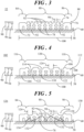
- FIG. 3 shows a side view of isolation wall 22 implemented in Doherty power amplifier 20 ( FIG. 1 ) useful for understanding some features of the invention.
- Isolation wall 22 includes a lower edge 72 and an upper edge 74 spaced apart by a body 76 of electrically conductive material.
- lower edge 72 of isolation wall 22 is configured to attach to or otherwise be in electrical communication with ground plane 60.
- Isolation wall 22 thus extends perpendicularly from surface 58 of ground plane 60.
- body 76 of isolation wall 22 may have a plurality of small holes 78 through which encapsulation material may flow during the packaging process. The size of holes 78 is sufficiently small so as not to adversely affect the electromagnetic isolation provided by isolation wall 22.
- Upper edge 74 of isolation wall 22 has a notched profile 80 of indentations 82 that extend toward lower edge 72 of isolation wall 72. More particularly, upper edge 74 of isolation wall 22 includes opposing first and second distal regions 84, 86 and a center region 88 interposed between distal regions 84, 86. Indentations 82 are located at center region 88 of isolation wall 22. Upper edge 74 of isolation wall 22 is spaced apart from surface 58 of ground plane 60 by a height 90 and a bottom portion 92 of each of indentations 82 is spaced apart from surface 58 by a height 94 that is less than height 90.
- first and second distal regions 116, 118 of isolation wall 102 may be spaced apart from surface 58 of ground plane 60 by height 96 that is less than height 90 of upper edge 106 but greater than height 94 of bottom portion 122 of indentations 114.
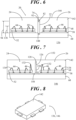
- FIG. 6 shows a simplified cross section view, useful for understanding some features of the invention, taken along line A-A in FIG. 2 showing Doherty power amplifier 20 with isolation wall 22 in a semiconductor device package 136. Isolation wall 22 is erected between carrier amplifier 24 and peaking amplifier 26 on ground plane 60.
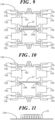
- FIG. 9 shows a top view of an example of a lead frame 154 for a semiconductor device package with isolation wall 22 formed by part of lead frame 154, useful for understanding some features of the invention.
- FIG. 10 shows a top view of lead frame 154 with isolation wall 22 bent upward into a final position
- FIG. 11 shows a side view of lead frame 154 with the bent isolation wall 22.
- Lead frame 154 is fabricated in a conventional manner from a flat electrically conductive sheet.
- isolation wall 22 is twisted by a particular amount (in some embodiments, approximately 90 degrees) about serpentine links 160 into the desired final position of isolation wall 22, which can be perpendicular to the plane of the remainder 162 of lead frame 154.
- Serpentine links 160 connecting isolation wall 22 to the pair of ground fingers 158 connects isolation wall 22 to ground or a reference potential during operation of the Doherty power amplifier 20 ( FIG. 1 ).
Landscapes
- Engineering & Computer Science (AREA)
- Power Engineering (AREA)
- Microelectronics & Electronic Packaging (AREA)
- Amplifiers (AREA)
- Physics & Mathematics (AREA)
- Health & Medical Sciences (AREA)
- Electromagnetism (AREA)
- Toxicology (AREA)
- Manufacturing & Machinery (AREA)
- Microwave Amplifiers (AREA)
Description
- The present disclosure relates generally to semiconductor device packages, and more specifically, to a semiconductor device package incorporating a structure to reduce inductive coupling between adjacent circuits therein.
- Wireless communication systems often employ power amplifiers for increasing the power of a signal. In a wireless communication system, a power amplifier is usually the last amplifier in a transmission chain (the output stage) and it is the amplifier stage that typically demands the most attention to power efficiency. High gain, high linearity, stability, and a high level of power-added efficiency (i.e., the ratio of the difference between the output power and the input power to DC power) are characteristics of an ideal amplifier.
EP2892076 describes a semiconductor device with a first and second circuit, with an isolation wall between the two circuits to reduce electromagnetic coupling between the circuits.US2012/025356 also describes a semiconductor device with two circuits separated by an isolation wall.US2007/246825 discloses a high frequency module and a manufacturing method thereof. In the module, a substrate has a ground. A plurality of surface mounted devices are mounted on the substrate. A metal wall is connected to the ground of the substrate. A resin molding hermetically seals the surface mounted devices and the metal wall. The metal wall features a lightning rod structure having a planar main board in a lower part thereof and a plurality of fingers in an upper part thereof, which define a plurality of indentations. - The invention is defined by the independent claims. Various optional features are described in the dependent claims.
- The accompanying figures in which like reference numerals refer to identical or functionally similar elements throughout the separate views, the figures are not necessarily drawn to scale, and which together with the detailed description below are incorporated in and form part of the specification, serve to further illustrate various embodiments and to explain various principles and advantages in accordance with the present invention.
-
FIG. 1 shows a simplified block diagram of a Doherty power amplifier with an isolation wall; -
FIG. 2 shows a top schematic view of components of carrier and peaking amplifiers for the Doherty power amplifier ofFIG. 1 ; -
FIG. 3 shows a side view of an isolation wall implemented in the semiconductor device ofFIG. 1 ; -
FIG. 4 shows a side view of an isolation wall; -
FIG. 5 shows a side view of an isolation wall in accordance with an embodiment; -
FIG. 6 shows a simplified cross section view taken along line A-A inFIG. 2 showing the Doherty amplifier -
FIG. 7 shows a simplified cross section view taken along line A-A inFIG. 2 showing the Doherty amplifier with an embodiment of the isolation wall in a semiconductor device package; -
FIG. 8 shows a perspective view of a completed semiconductor device package with the circuitry ofFIG. 1 encapsulated in an encapsulation material; -
FIG. 9 shows a top view of a lead frame for a semiconductor device package with the isolation wall formed by part of the lead frame; -
FIG. 10 shows a top view of the lead frame ofFIG. 9 with the isolation wall bent upward into a final position; and -
FIG. 11 shows a side view of the lead frame ofFIG. 9 with the bent isolation wall. - In overview, embodiments disclosed herein entail a semiconductor device package that incorporates a structure, i.e., an isolation wall, to reduce inductive coupling between elements of a semiconductor device embodied within the package. For a multi-path power amplifier (such as a Doherty power amplifier), an isolation wall that separates carrier amplifier elements from peaking amplifier elements is included within the semiconductor device package. The isolation wall can take the form of a structure that is constructed of a conductive material coupled to ground which separates the elements of the amplifier. Thus, the isolation wall can yield a significant improvement in signal isolation between amplifier elements, thereby improving performance of the multi-path amplifier. Additionally, the isolation wall has a notched profile of indentations along its upper edge that enables a less restricted flow of encapsulation material during fabrication. A less restricted flow of encapsulation material during fabrication may largely eliminate interior defects and/or surface defects on the completed package where visual inspection and part marking is likely to be performed.
- The terms "first," "second," "third," "fourth" and the like in the description and the claims, if any, may be used for distinguishing between similar elements and not necessarily for describing a particular sequential or chronological order. It is to be understood that the terms so used are interchangeable under appropriate circumstances such that the embodiments of the invention described herein are, for example, capable of operation in sequences other than those illustrated or otherwise described herein. Reference herein to directional relationships, such as top and bottom or left and right, refer to the relationship of the components in the orientation illustrated in the drawings, which may not be the orientation of the components in all uses of the apparatus being described. Furthermore, the terms "comprise," "include," "have" and any variations thereof, are intended to cover non-exclusive inclusions, such that a process, method, article, or apparatus that comprises a list of elements is not necessarily limited to those elements, but may include other elements not expressly listed or inherent to such process, method, article, or apparatus. The term "coupled," as used herein, is defined as directly or indirectly connected in an electrical or non-electrical manner.
- Referring to
FIG. 1, FIG. 1 shows a simplified block diagram of a Dohertypower amplifier 20 with anisolation wall 22. Dohertypower amplifier 20 includes a first circuit in the form of acarrier amplifier 24 and a second circuit in the form of a peakingamplifier 26. Aninput signal 28 is split into two signals by aninput splitter 30, which may apply a phase delay to one of the signals (e.g., a 90 degree phase delay). One of the resulting input signals is applied to afirst input 32 ofcarrier amplifier 24, and the other input signal is applied to asecond input 34 ofpeaking amplifier 26.Carrier amplifier 24 produces a first output signal at afirst output 36 andpeaking amplifier 26 produces a second output signal at asecond output 38. In a Doherty configuration,first input 32 and thefirst output 36 may constitute a gate terminal and a drain terminal ofcarrier amplifier 24, respectively. Similarly,second input 34 andsecond output 38 may constitute a gate terminal and a drain terminal of peakingamplifier 26, respectively. The first and second output signals are combined through a power combiner 40 to produce a combinedoutput signal 42. Those skilled in the art will recognize that a Doherty power amplifier semiconductor package typically includes additional electronic devices and circuitry not shown herein for simplicity of illustration. - In an example,
carrier amplifier 24 is configured to be active for an entire range of output powers of Dohertypower amplifier 20.Peaking amplifier 26 is configured to turn on only whencarrier amplifier 24 saturates.Peaking amplifier 26 delivers current ascarrier amplifier 24 saturates, thereby reducing the impedance seen at the output ofcarrier amplifier 24. Thus,carrier amplifier 24 delivers more current to the load whilecarrier amplifier 24 is saturated because of a "load-pulling" effect. Sincecarrier amplifier 24 remains close to saturation, Dohertypower amplifier 20 is able to transmit peak output power so that the total efficiency of the system remains relatively high. - Power combiner 40, operating to combine the first output signal from
carrier amplifier 24 with the second output signal frompeaking amplifier 26, may include a quarter-wave impedance inverter. The quarter-wave impedance inverter can add a ninety degree lag to the output signal fromcarrier amplifier 24 or peakingamplifier 26 in order to compensate for the phase delay added by the input splitter to the signal provided to either peakingamplifier 26 orcarrier amplifier 24. The phase of the signal provided to peakingamplifier 26 is typically designed to lag that ofcarrier amplifier 24 by ninety degrees so that the two output signals add in-phase when the output signals are combined at the output of power combiner 40 to form combinedoutput signal 42. - In the exemplary circuit in
FIG. 1 , each ofcarrier amplifier 24 and peakingamplifier 26 may include a number of active and passive electrical elements. For example,carrier amplifier 24 may include a first capacitor that couplesfirst input 32 to a first transistor, which applies the appropriate amplification to the first input signal received atfirst input 32. An output of the first transistor can be connected to a second capacitor. The first and second capacitors operate to condition the first input signal that is amplified by the first transistor. Similarly, peakingamplifier 26 can include a third capacitor couplingsecond input 34 to a second transistor, which applies the appropriate amplification to the second input signal received atsecond input 34. An output of the second transistor can be connected to a fourth capacitor. The third and fourth capacitors operate to condition the input second signal that is amplified by the second transistor. Those skilled in the art will recognize thatcarrier amplifier 24 and peakingamplifier 26 may include additional integrated active and/or passive electronic components not shown herein for simplicity of illustration. -
FIG. 2 shows a top schematic view of components of carrier and peakingamplifiers Doherty power amplifier 20. The separate electrical devices making upcarrier amplifier 24 and peakingamplifier 26 are connected to one another using multiple arrays ofinterconnects carrier amplifier 24 may be established using a first array ofinterconnects 44. Likewise, a second array ofinterconnects 46 may be used to establish one or more of the signal paths of peakingamplifier 26. -
Carrier amplifier 24 includes a number of integrated active and/or passive electrical components, such ascapacitors gate pad 54 and a drain pad 56) manufactured on and/or subsequently mounted to asurface 58 of a common (i.e., single) substrate, such as apackage ground plane 60.Capacitors ground plane 60. Similarly, peakingamplifier 26 includes a number of electrical devices, such ascapacitors gate pad 68 and a drain pad 70) manufactured on or subsequently mounted to surface 58 of a common (i.e., single) carrier, such aspackage ground plane 60.Capacitors ground plane 60. - The layout of the depicted
Doherty power amplifier 20 can result in the components ofcarrier amplifier 24 being adjacent to corresponding components of peakingamplifier 26. Accordingly, the arrangement of various components of each amplifier (including, specifically, first and second arrays ofinterconnects Doherty power amplifier 20 can result in some inductive coupling between carrier and peakingamplifiers interconnects - Therefore,
Doherty power amplifier 20 includesisolation wall 22 formed betweencarrier amplifier 24 and peakingamplifier 26 to provide electrical isolation between the circuits, their associated arrays of interconnects, and other components of carrier and peakingamplifiers Isolation wall 22, as described in greater detail below, is constructed as a body between the circuitry ofcarrier amplifier 24 and the circuitry of peakingamplifier 26. The material ofisolation wall 22 suitably conducts, absorbs, or reflects electromagnetic emissions from either or both ofcarrier amplifier 24 or peakingamplifier 26 thereby preventing the emissions from reaching the other amplifier.Isolation wall 22 may be built on various substrates or a lead frame of the semiconductor device depending upon the particular package design implementation. In various implementations,isolation wall 22 may be connected directly toground plane 60 or to a ground terminal which may, in turn be connected to a ground potential during operation ofDoherty power amplifier 20. In general, theisolation wall 22 operates as a shield to interrupt and prevent the inductive coupling betweencarrier amplifier 24 and peakingamplifier 26 ofDoherty power amplifier 20. - Along with the other components in a semiconductor device package that includes
Doherty power amplifier 20,isolation wall 22 may be over molded with a conventional encapsulation material to form a semiconductor device package. During an over molding process, the encapsulation material typically flows from one corner (i.e., mold gate) of a circuit such asDoherty power amplifier 20 over the entire body. Under such a scenario, taller components such as an isolation wall could potentially create an obstacle to the flow pattern of the encapsulation material. A restricted flow pattern could adversely affect adhesion and uniformity of the encapsulation material and/or could produce visual anomalies on the top surface of the semiconductor device package where part marking is typically performed. In accordance with various examples and embodiments described herein,isolation wall 22 is suitably shaped to enable a less restricted flow of encapsulation material during fabrication without adversely affecting the electromagnetic isolation achieved using an isolation wall. An improved flow of encapsulation material during fabrication may improve the quality of encapsulation material adhesion, uniformity of particle dispersion, and may largely eliminate interior and/or surface defects on the completed semiconductor device package. -
FIG. 3 shows a side view ofisolation wall 22 implemented in Doherty power amplifier 20 (FIG. 1 ) useful for understanding some features of the invention.Isolation wall 22 includes alower edge 72 and anupper edge 74 spaced apart by abody 76 of electrically conductive material. As will be discussed in greater detail below,lower edge 72 ofisolation wall 22 is configured to attach to or otherwise be in electrical communication withground plane 60.Isolation wall 22 thus extends perpendicularly fromsurface 58 ofground plane 60. In some configurations,body 76 ofisolation wall 22 may have a plurality ofsmall holes 78 through which encapsulation material may flow during the packaging process. The size ofholes 78 is sufficiently small so as not to adversely affect the electromagnetic isolation provided byisolation wall 22. -
Upper edge 74 ofisolation wall 22 has a notchedprofile 80 ofindentations 82 that extend towardlower edge 72 ofisolation wall 72. More particularly,upper edge 74 ofisolation wall 22 includes opposing first and seconddistal regions center region 88 interposed betweendistal regions Indentations 82 are located atcenter region 88 ofisolation wall 22.Upper edge 74 ofisolation wall 22 is spaced apart fromsurface 58 ofground plane 60 by aheight 90 and abottom portion 92 of each ofindentations 82 is spaced apart fromsurface 58 by aheight 94 that is less thanheight 90. As illustrated, first and seconddistal regions isolation wall 22 may be spaced apart fromsurface 58 ofground plane 60 by aheight 96 that is less thanheight 90 ofupper edge 74 but greater thanheight 94 ofbottom portion 92 ofindentations 82. Each ofindentations 82 is characterized by awidth 98 that is parallel to alengthwise dimension 100 ofisolation 22. Thus,width 98 is generally the same for each ofindentations 82. - The particular notched
profile 80 ofisolation wall 22 that includes thelower height 96 of first and seconddistal regions indentations 82 of a predetermined depth (i.e., the difference betweenheight 90 and height 94) andwidth 98 facilitates a flow of encapsulation material acrossisolation wall 22 during fabrication. This less restricted flow of encapsulation material may enable a more uniform distribution of particulates of various sizes within the encapsulation material on opposing sides ofisolation wall 22, may improve the quality of encapsulation material adhesion, and may largely eliminate interior and/or visual defects on the surface of the encapsulation material of the completed semiconductor device package where part marking is likely to be performed. However,width 98 ofindentations 82 is sufficiently narrow so thatisolation wall 22 functions as a solid wall in order to effectively reduce inductive coupling between carrier amplifier 24 (FIG. 1 ) and peaking amplifier (26).FIG. 4 shows a side view of anisolation wall 102, useful for understanding some features of the invention.Isolation wall 102 includes alower edge 104 and anupper edge 106 spaced apart by abody 108 of electrically conductive material. Likeisolation wall 22,lower edge 104 ofisolation wall 102 is configured to attach to or otherwise be in electrical communication withground plane 60 so thatisolation wall 102 extends perpendicularly fromsurface 58 ofground plane 60.Body 108 ofisolation wall 102 may additionally include a plurality ofsmall holes 110 through which encapsulation material may flow during the packaging process. -
Upper edge 106 ofisolation wall 102 has a notchedprofile 112 ofindentations 114 that extend towardlower edge 104 ofisolation wall 102. Again,upper edge 106 includes opposing first and seconddistal regions center region 120 interposed betweendistal regions Indentations 114 are located atcenter region 120 ofisolation wall 102.Upper edge 106 ofisolation wall 102 is spaced apart fromsurface 58 ofground plane 60 byheight 90 and abottom portion 122 of each ofindentations 114 is spaced apart fromsurface 58 byheight 94 that is less thanheight 90. As illustrated, first and seconddistal regions isolation wall 102 may be spaced apart fromsurface 58 ofground plane 60 byheight 96 that is less thanheight 90 ofupper edge 106 but greater thanheight 94 ofbottom portion 122 ofindentations 114. - Each of
indentations 114 is characterized by awidth 124 that is parallel tolengthwise dimension 100 ofisolation wall 102. Thus,width 124 is generally the same for each ofindentations 114.Isolation wall 102 provides an example in whichindentations 114 havewidth 124 that is greater than width 98 (FIG. 3 ) ofindentations 82 of isolation wall 22 (FIG. 3 ). Thegreater width 124 ofindentations 114 relative towidth 98 ofindentations 82 may more effectively enable the flow of encapsulation material acrossisolation wall 102. However, due to thegreater width 124 ofindentations 114, such anisolation wall 102 may be implemented in a semiconductor device package in which electrical circuits (e.g., a carrier amplifier and a peaking amplifier) are located at relatively large distances from one another so that electrical performance of the semiconductor device package is not significantly worsened. -
FIG. 5 shows a side view of anisolation wall 126 in accordance with an embodiment.FIG. 5 represents a configuration in which anupper edge 128 ofisolation wall 126 includes a notchedprofile 130 having bothindentations 82 ofwidth 98 andindentations 114 ofwidth 124. Thus,isolation wall 126 represents a compromise between the features of isolation wall 22 (FIG. 3 ) and isolation wall 102 (FIG. 4 ). -
FIG. 5 further includes dottedlines Dotted lines interconnects 44, 46 (FIG. 2 ) that may be included in Doherty power amplifier 20 (FIG. 2 ). More particularly, dashedlines 132 represent interconnects (e.g., shunt wires) that are taller than the remaining interconnects and dashedlines 134 represent the shorter remaining interconnects. Dashedlines ground plane 60, and the like. - In accordance with the illustrated embodiment,
isolation wall 126 may be formed to include thenarrower indentations 82 closer to thetaller interconnects 132 to provide effective electrical isolation. Additionally,isolation wall 126 may be formed to include thewider indentations 114 at the regions of theshorter interconnects 134 to achieve acceptable electrical isolation while concurrently facilitating the flow of encapsulation material overisolation wall 126. -
FIGs. 3-5 are provided to demonstrate various notched profiles of the upper edge of the isolation walls. Other notched profiles may be implemented that provide effective electromagnetic isolation while concurrently facilitating the flow of encapsulation material over isolation wall. The lower edges of any ofisolation walls ground plane 60. Thus,FIGs. 6-11 (described below) are provided to demonstrate example attachment techniques. However, other attachment techniques may be implemented as well. -
FIG. 6 shows a simplified cross section view, useful for understanding some features of the invention, taken along line A-A inFIG. 2 showingDoherty power amplifier 20 withisolation wall 22 in asemiconductor device package 136.Isolation wall 22 is erected betweencarrier amplifier 24 and peakingamplifier 26 onground plane 60. - According to various examples,
isolation wall 22 is positioned perpendicular toground plane 60 and extends some distance above amaximum height 138 of the various components ofcarrier amplifier 24 and peaking amplifier 26 (and their associated first and second arrays ofinterconnects 44, 46). By way of example,maximum height 138 may be less thanheight 94 ofbottom portions 92 ofindentations 82. - In the example of
FIG. 6 , electricallyconductive isolation wall 22 may be inserted into a slot oraperture 140 inground plane 60, thereby making electrical connection toground plane 60 which is a ground node insemiconductor device 136.Slot 140 may be formed withinground plane 60 by any suitable etching or material removal process. Thereafter, an encapsulation material 142 (also known as mold compound, molding compound, or encapsulant) coverssurface 58 ofground plane 60, carrier andpeak amplifiers interconnects isolation wall 22.Upper edge 74 ofisolation wall 22 may be spaced slightly away from atop surface 144 ofsemiconductor device package 136 so that someencapsulation material 142 extends acrossisolation wall 22 as shown inFIG. 6 . -
FIG. 7 shows a simplified cross section view taken along line A-A inFIG. 2 showingDoherty power amplifier 20 withisolation wall 126 in asemiconductor device package 146. In this illustrated example,isolation wall 126 includes a bottom section that is bent to form abase 148 extending perpendicular to abody 150 ofisolation wall 126.Base 148 supportsisolation wall 126 onsurface 58 ofground plane 60.Base 148 may, in some cases, be used as a substitute forslot 140 inground plane 60 as shown inFIG. 6 .Base 148 is secured in a manner that establishes electrical contact withground plane 60, or ground node. For example,base 148 may be soldered, brazed, or attached by an electrically conductive adhesive or epoxy toground plane 60. Alternatively, any of conductive isolation walls 22 (FIG. 3 ), 102 (FIG. 4 ), or 126 may be attached to a ground pad, a ground conductor, or other ground node of the circuitry within any of the semiconductor device packages. -
Semiconductor device package 146 is depicted withisolation wall 126 that may include notched profile 130 (best seen inFIG. 5 ) having wider indentations 114 (FIG. 5 ) located at regions ofshorter interconnects 44, 46 (also labeled 134 to correspond with their depiction inFIG. 5 ) andnarrower indentations 82 at located at regions oftaller interconnects 44, 46 (also labeled 132 to correspond with their depiction inFIG. 5 ).Encapsulation material 142 covers surface 58 ofground plane 60, carrier andpeak amplifiers interconnects isolation wall 22.Upper edge 128 ofisolation wall 126 may be spaced slightly away from atop surface 152 ofsemiconductor device package 146 so that someencapsulation material 142 extends acrossisolation wall 126 as shown inFIG. 7 . - Isolation wall 22 (depicted in
FIG. 6 ) and isolation wall 126 (depicted inFIG. 7 ) are both shown in physical contact withground plane 60. However, an isolation wall need not be in direct physical contact withground plane 60. In alternative embodiments, isolation wall may be slightly above (i.e., spaced apart from)ground plane 60, but still tied electrically to a common ground node. -
FIG. 8 shows a perspective view of a completed semiconductor device package (e.g., either ofsemiconductor packages 136, 146) with the circuitry ofFIG. 1 encapsulated inencapsulation material 142. Each of the notched profiles of any of isolation walls 22 (FIG. 3 ), 102 (FIG. 4 ), or 126 (FIG. 5 ) facilitates the flow ofencapsulation material 142 acrossisolation wall 126 during fabrication so that the top surface of the semiconductor device package is largely free of surface defects. - With reference to
FIGs. 9-11, FIG. 9 shows a top view of an example of alead frame 154 for a semiconductor device package withisolation wall 22 formed by part oflead frame 154, useful for understanding some features of the invention.FIG. 10 shows a top view oflead frame 154 withisolation wall 22 bent upward into a final position, andFIG. 11 shows a side view oflead frame 154 with thebent isolation wall 22.Lead frame 154 is fabricated in a conventional manner from a flat electrically conductive sheet. - In an example,
lead frame 154 has a plurality oflead fingers 156 and a pair ofground fingers 158 which may be connected to ground node in a semiconductor device package. In other configurations,lead frame 154 may be connected to a ground node through an outside circuit, such as a printed circuit board (PCB).Isolation wall 22 is formed in the center of thelead frame 154 withserpentine links 160 at each end connectingisolation wall 22 to the pair ofground fingers 158.Isolation wall 22 is initially formed coplanar with theremainder 162 oflead frame 154. Prior to assembly of the semiconductor device package,isolation wall 22 is bent transverse to the plane oflead frame 154 as shown inFIGs. 10 and 11 . Specifically,isolation wall 22 is twisted by a particular amount (in some embodiments, approximately 90 degrees) aboutserpentine links 160 into the desired final position ofisolation wall 22, which can be perpendicular to the plane of theremainder 162 oflead frame 154.Serpentine links 160 connectingisolation wall 22 to the pair ofground fingers 158 connectsisolation wall 22 to ground or a reference potential during operation of the Doherty power amplifier 20 (FIG. 1 ).
Claims (10)
- A semiconductor device package comprising:a support being a one of a substrate, or a lead frame (154) which lead frame has, in the same plane, a flat portion, a plurality of lead fingers (156) and a pair of ground fingers (158);a first circuit mounted on said substrate or on said flat portion of said lead frame, said first circuit comprising a first plurality of electrical components;a second circuit mounted on said substrate or on said flat portion of said lead frame, said second circuit comprising a second plurality of electrical components;an isolation wall (22, 102, 126) located between said first circuit and said second circuit, said isolation wall, when said support is a substrate, extending perpendicularly from a surface of said substrate above a height of said first plurality of components and said second plurality of components, or, when said support is a lead frame, being a bent portion of the lead frame extending perpendicularly from the flat portion thereof and being in contact with said ground fingers, said isolation wall having an upper edge (74, 106, 128), andencapsulation material (142) covering said surface of said substrate or said flat portion of said lead frame, and said first and second circuits wherein said upper edge has a notched profile (80, 112, 130) of indentations (82, 114) extending toward said surface of said substrate;
wherein said indentations comprise:first indentations (82), each of said first indentations exhibiting a first width (98) parallel to a lengthwise dimension of said isolation wall;second indentations (114), each of said second indentations exhibiting a second width (124) parallel to said lengthwise dimension of said isolation wall, said second width being greater than said first width;said first circuit includes a first transistor and a first array of interconnects (44), being bond wires, electrically coupled between said first transistor and respective ones of first leads of said substrate or respective ones of said lead fingers of the lead frame; andsaid second circuit includes a second transistor and a second array of interconnects (46), being bond wires, electrically coupled between said second transistor and respective ones of second leads of said substrate or respective ones of said lead fingers of the lead frame, said isolation wall is positioned between said first and second arrays of interconnects, at least one of said interconnects of said first and second arrays of interconnects is taller than the remainder of said interconnects of said first and second arrays of interconnects, and said first indentations are formed in said isolation wall to be closer to said at least one of said interconnects that is taller than the remainder of said interconnects than said second indentations. - The semiconductor device package of claim 1, wherein said height is a first height, said upper edge of said isolation wall is spaced apart from said surface of said substrate or said flat portion of said lead frame by a second height (90), and a bottom portion (92, 122) of each of said indentations is spaced apart from said surface of said substrate or said flat portion of said lead frame by a third height (94), said third height being less than said second height.
- The semiconductor device package of claim 2, wherein said first height of said first plurality of components and said second plurality of components is less than said third height.
- The semiconductor device package of any one of the claims 1 to 3, wherein said height is a first height, said upper edge of said isolation wall includes opposing first and second distal regions (84, 116; 86, 118) and a center region (80, 120) interposed between said first and second distal regions, said indentations are located at said center region of said upper edge of said isolation wall, said upper edge of said isolation wall at said center region is spaced apart from said surface of said substrate or said flat portion of said lead frame by a second height, and first and second distal regions of said upper edge are spaced apart from said surface of said substrate or said flat portion of said lead frame by a third height, said third height being less than said second height.
- The semiconductor device package of any one of the claims 1 to 4, further comprising a ground potential node, wherein, when the support is a lead frame, said isolation wall is electrically connected to said ground potential node.
- The semiconductor device package of any one of the claims 1 to 5, wherein said isolation wall is configured to reduce inductive coupling between said first circuit and said second circuit during operation of at least one of said first and second circuits.
- The semiconductor device package of any one of the claims 1 to 6, wherein said isolation wall is formed from a body of electrically conductive material.
- The semiconductor device package of any one of the claims 1 to 7, wherein said encapsulation material covers said isolation wall, and said indentations facilitate a flow of said encapsulation material across said isolation wall during fabrication.
- The semiconductor device package of any one of the claims 1 to 8, wherein:said first circuit includes a carrier amplifier (24) of a Doherty amplifier; andsaid second circuit includes a peaking amplifier (26) of said Doherty amplifier.
- A method of fabricating a semiconductor device package comprising:providing a support being a one of a substrate, or a lead frame (154) which lead frame has, in the same plane, a flat portion, a plurality of lead fingers, (156) and a pair of ground fingers (158);mounting a first circuit on a surface of said substrate or on said flat portion of said lead frame, said first circuit including a first plurality of components;mounting a second circuit on said surface of said substrate or on said flat portion of said lead frame, adjacent to said first circuit, said second circuit including a second plurality of components;locating an isolation wall (22, 102, 126) of electrically conductive material between said first circuit and said second circuit, said isolation wall, when the support is said substrate, extending perpendicularly from a surface of said substrate above a height of said first plurality of components and said second plurality of components, or when said support is a lead frame, being a bent portion of the lead frame extending perpendicularly from the flat potion thereof and being in contact with said ground fingers, said isolation wall having an upper edge(74, 106, 128), said upper edge having a notched profile (80, 112, 130) of indentations (82, 114) extending toward said surface of said substrate, said isolation wall being configured to reduce inductive coupling between said first circuit and said second circuit during operation of said semiconductor device; andcovering said surface of said substrate, or said flat portion of said lead frame, and said first and second circuits with encapsulation material;wherein said indentations comprise:first indentations (82), each of said first indentations exhibiting a first width (98) parallel to a lengthwise dimension of said isolation wall;second indentations (114), each of said second indentations exhibiting a second width (124) parallel to said lengthwise dimension of said isolation wall, said second width being greater than said first width; andsaid first circuit includes a first transistor and a first array of interconnects (44), being bond wires, electrically coupled between said first transistor and respective ones of first leads of said substrate or respective ones of said lead fingers of the lead frame; andsaid second circuit includes a second transistor and a second array of interconnects (46), being bond wires, electrically coupled between said second transistor and respective ones of second leads of said substrate or respective ones of said lead fingers of the lead frame, said isolation wall is positioned between said first and second arrays of interconnects, at least one of said interconnects of said first and second arrays of interconnects is taller than the remainder of said interconnects of said first and second arrays of interconnects, and said first indentations are formed in said isolation wall to be closer to said at least one of said interconnects that is taller than the remainder of said interconnects than said second indentations.
Applications Claiming Priority (1)
| Application Number | Priority Date | Filing Date | Title |
|---|---|---|---|
| US15/052,229 US9607953B1 (en) | 2016-02-24 | 2016-02-24 | Semiconductor package with isolation wall |
Publications (2)
| Publication Number | Publication Date |
|---|---|
| EP3211669A1 EP3211669A1 (en) | 2017-08-30 |
| EP3211669B1 true EP3211669B1 (en) | 2025-04-09 |
Family
ID=57965830
Family Applications (1)
| Application Number | Title | Priority Date | Filing Date |
|---|---|---|---|
| EP17154795.3A Active EP3211669B1 (en) | 2016-02-24 | 2017-02-06 | Semiconductor package with isolation wall |
Country Status (3)
| Country | Link |
|---|---|
| US (1) | US9607953B1 (en) |
| EP (1) | EP3211669B1 (en) |
| CN (1) | CN107123637B (en) |
Families Citing this family (13)
| Publication number | Priority date | Publication date | Assignee | Title |
|---|---|---|---|---|
| US10629552B2 (en) * | 2018-04-30 | 2020-04-21 | Nxp Usa, Inc. | Amplifiers and amplifier modules with ground plane height variation structures |
| US10763334B2 (en) | 2018-07-11 | 2020-09-01 | Cree, Inc. | Drain and/or gate interconnect and finger structure |
| US10600746B2 (en) | 2018-07-19 | 2020-03-24 | Cree, Inc. | Radio frequency transistor amplifiers and other multi-cell transistors having gaps and/or isolation structures between groups of unit cell transistors |
| US10770415B2 (en) | 2018-12-04 | 2020-09-08 | Cree, Inc. | Packaged transistor devices with input-output isolation and methods of forming packaged transistor devices with input-output isolation |
| EP3723282B1 (en) * | 2019-04-12 | 2024-12-18 | NXP USA, Inc. | Power amplifier packages and systems incorporating design-flexible package platforms |
| US11417746B2 (en) | 2019-04-24 | 2022-08-16 | Wolfspeed, Inc. | High power transistor with interior-fed fingers |
| US11011813B2 (en) * | 2019-07-12 | 2021-05-18 | Nxp B.V. | Power amplifier with shielded transmission lines |
| US11355451B2 (en) | 2019-08-28 | 2022-06-07 | Amkor Technology Singapore Holding Pte. Ltd. | Semiconductor devices and methods of manufacturing semiconductor devices |
| US11004801B2 (en) * | 2019-08-28 | 2021-05-11 | Amkor Technology Singapore Holding Pte. Ltd. | Semiconductor devices and methods of manufacturing semiconductor devices |
| US11121072B1 (en) | 2020-03-16 | 2021-09-14 | Nxp Usa, Inc. | Semiconductor device with isolation structure |
| US12531554B2 (en) * | 2023-02-27 | 2026-01-20 | Rtx Corporation | Enhanced solid state circuit breaker structure |
| US12446158B2 (en) | 2023-10-13 | 2025-10-14 | Nxp Usa, Inc. | Circuit modules with encapsulant-embedded leadframe terminals, and methods of fabricating such circuit modules |
| CN120454753B (en) * | 2025-07-11 | 2025-10-03 | 成都晶宝时频技术股份有限公司 | K-band radio frequency front-end receiving and transmitting processing module |
Citations (1)
| Publication number | Priority date | Publication date | Assignee | Title |
|---|---|---|---|---|
| US20070246825A1 (en) * | 2006-04-21 | 2007-10-25 | Samsung Electro-Mechanics Co., Ltd. | High frequency module using metal-wall and method of manufacturing the same |
Family Cites Families (14)
| Publication number | Priority date | Publication date | Assignee | Title |
|---|---|---|---|---|
| US5482898A (en) | 1993-04-12 | 1996-01-09 | Amkor Electronics, Inc. | Method for forming a semiconductor device having a thermal dissipator and electromagnetic shielding |
| US5608188A (en) | 1994-09-02 | 1997-03-04 | Motorola, Inc. | Multi compartment electromagnetic energy shield |
| KR0144164B1 (en) * | 1995-05-12 | 1998-07-01 | 문정환 | How to package ELC semiconductor package and semiconductor device |
| US5661337A (en) | 1995-11-07 | 1997-08-26 | Vlsi Technology, Inc. | Technique for improving bonding strength of leadframe to substrate in semiconductor IC chip packages |
| JP3505488B2 (en) | 1999-10-12 | 2004-03-08 | 古河電気工業株式会社 | Optical module |
| US6614102B1 (en) * | 2001-05-04 | 2003-09-02 | Amkor Technology, Inc. | Shielded semiconductor leadframe package |
| US7629674B1 (en) * | 2004-11-17 | 2009-12-08 | Amkor Technology, Inc. | Shielded package having shield fence |
| TWI540698B (en) * | 2010-08-02 | 2016-07-01 | 日月光半導體製造股份有限公司 | Semiconductor package and method of manufacturing same |
| CN102364683A (en) | 2011-10-21 | 2012-02-29 | 华为终端有限公司 | Packaging structure and method thereof, and electronic equipment |
| US9312817B2 (en) | 2012-07-20 | 2016-04-12 | Freescale Semiconductor, Inc. | Semiconductor package design providing reduced electromagnetic coupling between circuit components |
| US9357292B2 (en) * | 2012-12-06 | 2016-05-31 | Fortemedia, Inc. | Implementation of microphone array housing receiving sound via guide tube |
| EP2747134B1 (en) | 2012-12-18 | 2021-09-01 | Ampleon Netherlands B.V. | Amplifier device |
| US9401342B2 (en) * | 2013-06-27 | 2016-07-26 | Freescale Semiconductor, Inc. | Semiconductor package having wire bond wall to reduce coupling |
| US9450547B2 (en) | 2013-12-12 | 2016-09-20 | Freescale Semiconductor, Inc. | Semiconductor package having an isolation wall to reduce electromagnetic coupling |
-
2016
- 2016-02-24 US US15/052,229 patent/US9607953B1/en active Active
-
2017
- 2017-02-06 EP EP17154795.3A patent/EP3211669B1/en active Active
- 2017-02-20 CN CN201710091513.1A patent/CN107123637B/en active Active
Patent Citations (1)
| Publication number | Priority date | Publication date | Assignee | Title |
|---|---|---|---|---|
| US20070246825A1 (en) * | 2006-04-21 | 2007-10-25 | Samsung Electro-Mechanics Co., Ltd. | High frequency module using metal-wall and method of manufacturing the same |
Also Published As
| Publication number | Publication date |
|---|---|
| CN107123637B (en) | 2022-04-29 |
| CN107123637A (en) | 2017-09-01 |
| EP3211669A1 (en) | 2017-08-30 |
| US9607953B1 (en) | 2017-03-28 |
Similar Documents
| Publication | Publication Date | Title |
|---|---|---|
| US10630243B2 (en) | Semiconductor package having an isolation wall to reduce electromagnetic coupling | |
| US9607953B1 (en) | Semiconductor package with isolation wall | |
| CN108233876B (en) | Doherty amplifier with parallel inductance circuit and amplifier module | |
| EP3331161B1 (en) | Amplifier die with elongated side pads, and amplifier modules that incorporate such amplifier die | |
| US10269729B2 (en) | Semiconductor packages having wire bond wall to reduce coupling | |
| EP3247038B1 (en) | Multiple-path rf amplifiers with angularly offset signal path directions, and methods of manufacture thereof | |
| US9673164B2 (en) | Semiconductor package and system with an isolation structure to reduce electromagnetic coupling | |
| US10109594B2 (en) | Semiconductor device with an isolation structure coupled to a cover of the semiconductor device | |
| US9401342B2 (en) | Semiconductor package having wire bond wall to reduce coupling | |
| EP2879174B1 (en) | Packaged RF power transistor device having next to each other ground leads and a video lead for connecting decoupling capacitors, RF power amplifier | |
| US20190173430A1 (en) | Multiple-path amplifier with series component along inverter between amplifier outputs | |
| US11581241B2 (en) | Circuit modules with front-side interposer terminals and through-module thermal dissipation structures | |
| US10784209B2 (en) | Electrical component, device and package | |
| US20250349702A1 (en) | Capacitor networks for harmonic control in power devices | |
| US12512792B2 (en) | Radio frequency amplifier | |
| US11367696B2 (en) | Radio frequency amplifiers having improved shunt matching circuits | |
| JP5800360B2 (en) | Doherty amplifier | |
| JP2019176281A (en) | Amplifier and Doherty amplifier circuit |
Legal Events
| Date | Code | Title | Description |
|---|---|---|---|
| PUAI | Public reference made under article 153(3) epc to a published international application that has entered the european phase |
Free format text: ORIGINAL CODE: 0009012 |
|
| STAA | Information on the status of an ep patent application or granted ep patent |
Free format text: STATUS: THE APPLICATION HAS BEEN PUBLISHED |
|
| AK | Designated contracting states |
Kind code of ref document: A1 Designated state(s): AL AT BE BG CH CY CZ DE DK EE ES FI FR GB GR HR HU IE IS IT LI LT LU LV MC MK MT NL NO PL PT RO RS SE SI SK SM TR |
|
| AX | Request for extension of the european patent |
Extension state: BA ME |
|
| STAA | Information on the status of an ep patent application or granted ep patent |
Free format text: STATUS: REQUEST FOR EXAMINATION WAS MADE |
|
| 17P | Request for examination filed |
Effective date: 20180228 |
|
| RBV | Designated contracting states (corrected) |
Designated state(s): AL AT BE BG CH CY CZ DE DK EE ES FI FR GB GR HR HU IE IS IT LI LT LU LV MC MK MT NL NO PL PT RO RS SE SI SK SM TR |
|
| STAA | Information on the status of an ep patent application or granted ep patent |
Free format text: STATUS: EXAMINATION IS IN PROGRESS |
|
| 17Q | First examination report despatched |
Effective date: 20191216 |
|
| GRAP | Despatch of communication of intention to grant a patent |
Free format text: ORIGINAL CODE: EPIDOSNIGR1 |
|
| STAA | Information on the status of an ep patent application or granted ep patent |
Free format text: STATUS: GRANT OF PATENT IS INTENDED |
|
| RIC1 | Information provided on ipc code assigned before grant |
Ipc: H01L 23/495 20060101ALI20240925BHEP Ipc: H01L 21/56 20060101ALI20240925BHEP Ipc: H03F 1/02 20060101ALI20240925BHEP Ipc: H03F 3/195 20060101ALI20240925BHEP Ipc: H01L 23/16 20060101ALI20240925BHEP Ipc: H01L 25/065 20060101ALI20240925BHEP Ipc: H01L 23/552 20060101ALI20240925BHEP Ipc: H01L 23/66 20060101AFI20240925BHEP |
|
| INTG | Intention to grant announced |
Effective date: 20241022 |
|
| GRAS | Grant fee paid |
Free format text: ORIGINAL CODE: EPIDOSNIGR3 |
|
| GRAA | (expected) grant |
Free format text: ORIGINAL CODE: 0009210 |
|
| STAA | Information on the status of an ep patent application or granted ep patent |
Free format text: STATUS: THE PATENT HAS BEEN GRANTED |
|
| AK | Designated contracting states |
Kind code of ref document: B1 Designated state(s): AL AT BE BG CH CY CZ DE DK EE ES FI FR GB GR HR HU IE IS IT LI LT LU LV MC MK MT NL NO PL PT RO RS SE SI SK SM TR |
|
| REG | Reference to a national code |
Ref country code: GB Ref legal event code: FG4D |
|
| REG | Reference to a national code |
Ref country code: CH Ref legal event code: EP |
|
| REG | Reference to a national code |
Ref country code: DE Ref legal event code: R096 Ref document number: 602017088775 Country of ref document: DE |
|
| REG | Reference to a national code |
Ref country code: IE Ref legal event code: FG4D |
|
| REG | Reference to a national code |
Ref country code: NL Ref legal event code: MP Effective date: 20250409 |
|
| PG25 | Lapsed in a contracting state [announced via postgrant information from national office to epo] |
Ref country code: NL Free format text: LAPSE BECAUSE OF FAILURE TO SUBMIT A TRANSLATION OF THE DESCRIPTION OR TO PAY THE FEE WITHIN THE PRESCRIBED TIME-LIMIT Effective date: 20250409 |
|
| REG | Reference to a national code |
Ref country code: AT Ref legal event code: MK05 Ref document number: 1784373 Country of ref document: AT Kind code of ref document: T Effective date: 20250409 |
|
| PG25 | Lapsed in a contracting state [announced via postgrant information from national office to epo] |
Ref country code: PT Free format text: LAPSE BECAUSE OF FAILURE TO SUBMIT A TRANSLATION OF THE DESCRIPTION OR TO PAY THE FEE WITHIN THE PRESCRIBED TIME-LIMIT Effective date: 20250811 Ref country code: ES Free format text: LAPSE BECAUSE OF FAILURE TO SUBMIT A TRANSLATION OF THE DESCRIPTION OR TO PAY THE FEE WITHIN THE PRESCRIBED TIME-LIMIT Effective date: 20250409 Ref country code: FI Free format text: LAPSE BECAUSE OF FAILURE TO SUBMIT A TRANSLATION OF THE DESCRIPTION OR TO PAY THE FEE WITHIN THE PRESCRIBED TIME-LIMIT Effective date: 20250409 |
|
| REG | Reference to a national code |
Ref country code: LT Ref legal event code: MG9D |
|
| PG25 | Lapsed in a contracting state [announced via postgrant information from national office to epo] |
Ref country code: NO Free format text: LAPSE BECAUSE OF FAILURE TO SUBMIT A TRANSLATION OF THE DESCRIPTION OR TO PAY THE FEE WITHIN THE PRESCRIBED TIME-LIMIT Effective date: 20250709 Ref country code: GR Free format text: LAPSE BECAUSE OF FAILURE TO SUBMIT A TRANSLATION OF THE DESCRIPTION OR TO PAY THE FEE WITHIN THE PRESCRIBED TIME-LIMIT Effective date: 20250710 |
|
| PG25 | Lapsed in a contracting state [announced via postgrant information from national office to epo] |
Ref country code: PL Free format text: LAPSE BECAUSE OF FAILURE TO SUBMIT A TRANSLATION OF THE DESCRIPTION OR TO PAY THE FEE WITHIN THE PRESCRIBED TIME-LIMIT Effective date: 20250409 |
|
| PG25 | Lapsed in a contracting state [announced via postgrant information from national office to epo] |
Ref country code: BG Free format text: LAPSE BECAUSE OF FAILURE TO SUBMIT A TRANSLATION OF THE DESCRIPTION OR TO PAY THE FEE WITHIN THE PRESCRIBED TIME-LIMIT Effective date: 20250409 |
|
| PG25 | Lapsed in a contracting state [announced via postgrant information from national office to epo] |
Ref country code: HR Free format text: LAPSE BECAUSE OF FAILURE TO SUBMIT A TRANSLATION OF THE DESCRIPTION OR TO PAY THE FEE WITHIN THE PRESCRIBED TIME-LIMIT Effective date: 20250409 |
|
| PG25 | Lapsed in a contracting state [announced via postgrant information from national office to epo] |
Ref country code: AT Free format text: LAPSE BECAUSE OF FAILURE TO SUBMIT A TRANSLATION OF THE DESCRIPTION OR TO PAY THE FEE WITHIN THE PRESCRIBED TIME-LIMIT Effective date: 20250409 |
|
| PG25 | Lapsed in a contracting state [announced via postgrant information from national office to epo] |
Ref country code: RS Free format text: LAPSE BECAUSE OF FAILURE TO SUBMIT A TRANSLATION OF THE DESCRIPTION OR TO PAY THE FEE WITHIN THE PRESCRIBED TIME-LIMIT Effective date: 20250709 |
|
| PG25 | Lapsed in a contracting state [announced via postgrant information from national office to epo] |
Ref country code: IS Free format text: LAPSE BECAUSE OF FAILURE TO SUBMIT A TRANSLATION OF THE DESCRIPTION OR TO PAY THE FEE WITHIN THE PRESCRIBED TIME-LIMIT Effective date: 20250809 |
|
| PG25 | Lapsed in a contracting state [announced via postgrant information from national office to epo] |
Ref country code: LV Free format text: LAPSE BECAUSE OF FAILURE TO SUBMIT A TRANSLATION OF THE DESCRIPTION OR TO PAY THE FEE WITHIN THE PRESCRIBED TIME-LIMIT Effective date: 20250409 |
|
| REG | Reference to a national code |
Ref country code: DE Ref legal event code: R079 Ref document number: 602017088775 Country of ref document: DE Free format text: PREVIOUS MAIN CLASS: H01L0023660000 Ipc: H10W0044200000 |
|
| REG | Reference to a national code |
Ref country code: DE Ref legal event code: R097 Ref document number: 602017088775 Country of ref document: DE |
|
| PG25 | Lapsed in a contracting state [announced via postgrant information from national office to epo] |
Ref country code: DK Free format text: LAPSE BECAUSE OF FAILURE TO SUBMIT A TRANSLATION OF THE DESCRIPTION OR TO PAY THE FEE WITHIN THE PRESCRIBED TIME-LIMIT Effective date: 20250409 Ref country code: SM Free format text: LAPSE BECAUSE OF FAILURE TO SUBMIT A TRANSLATION OF THE DESCRIPTION OR TO PAY THE FEE WITHIN THE PRESCRIBED TIME-LIMIT Effective date: 20250409 |
|
| PG25 | Lapsed in a contracting state [announced via postgrant information from national office to epo] |
Ref country code: CZ Free format text: LAPSE BECAUSE OF FAILURE TO SUBMIT A TRANSLATION OF THE DESCRIPTION OR TO PAY THE FEE WITHIN THE PRESCRIBED TIME-LIMIT Effective date: 20250409 |
|
| PG25 | Lapsed in a contracting state [announced via postgrant information from national office to epo] |
Ref country code: EE Free format text: LAPSE BECAUSE OF FAILURE TO SUBMIT A TRANSLATION OF THE DESCRIPTION OR TO PAY THE FEE WITHIN THE PRESCRIBED TIME-LIMIT Effective date: 20250409 |
|
| PG25 | Lapsed in a contracting state [announced via postgrant information from national office to epo] |
Ref country code: RO Free format text: LAPSE BECAUSE OF FAILURE TO SUBMIT A TRANSLATION OF THE DESCRIPTION OR TO PAY THE FEE WITHIN THE PRESCRIBED TIME-LIMIT Effective date: 20250409 Ref country code: SK Free format text: LAPSE BECAUSE OF FAILURE TO SUBMIT A TRANSLATION OF THE DESCRIPTION OR TO PAY THE FEE WITHIN THE PRESCRIBED TIME-LIMIT Effective date: 20250409 |
|
| PG25 | Lapsed in a contracting state [announced via postgrant information from national office to epo] |
Ref country code: IT Free format text: LAPSE BECAUSE OF FAILURE TO SUBMIT A TRANSLATION OF THE DESCRIPTION OR TO PAY THE FEE WITHIN THE PRESCRIBED TIME-LIMIT Effective date: 20250409 |
|
| PLBE | No opposition filed within time limit |
Free format text: ORIGINAL CODE: 0009261 |
|
| STAA | Information on the status of an ep patent application or granted ep patent |
Free format text: STATUS: NO OPPOSITION FILED WITHIN TIME LIMIT |
|
| REG | Reference to a national code |
Ref country code: CH Ref legal event code: L10 Free format text: ST27 STATUS EVENT CODE: U-0-0-L10-L00 (AS PROVIDED BY THE NATIONAL OFFICE) Effective date: 20260218 |
|
| 26N | No opposition filed |
Effective date: 20260112 |
|
| PGFP | Annual fee paid to national office [announced via postgrant information from national office to epo] |
Ref country code: DE Payment date: 20260121 Year of fee payment: 10 |