EP3210934A1 - Micro-electro-mechanical type pressure device having low sensitivity to temperature - Google Patents
Micro-electro-mechanical type pressure device having low sensitivity to temperature Download PDFInfo
- Publication number
- EP3210934A1 EP3210934A1 EP16194672.8A EP16194672A EP3210934A1 EP 3210934 A1 EP3210934 A1 EP 3210934A1 EP 16194672 A EP16194672 A EP 16194672A EP 3210934 A1 EP3210934 A1 EP 3210934A1
- Authority
- EP
- European Patent Office
- Prior art keywords
- region
- face
- air gap
- forming
- buried cavity
- Prior art date
- Legal status (The legal status is an assumption and is not a legal conclusion. Google has not performed a legal analysis and makes no representation as to the accuracy of the status listed.)
- Granted
Links
Images


Classifications
-
- B—PERFORMING OPERATIONS; TRANSPORTING
- B81—MICROSTRUCTURAL TECHNOLOGY
- B81B—MICROSTRUCTURAL DEVICES OR SYSTEMS, e.g. MICROMECHANICAL DEVICES
- B81B3/00—Devices comprising flexible or deformable elements, e.g. comprising elastic tongues or membranes
- B81B3/0018—Structures acting upon the moving or flexible element for transforming energy into mechanical movement or vice versa, i.e. actuators, sensors, generators
- B81B3/0027—Structures for transforming mechanical energy, e.g. potential energy of a spring into translation, sound into translation
-
- B—PERFORMING OPERATIONS; TRANSPORTING
- B81—MICROSTRUCTURAL TECHNOLOGY
- B81B—MICROSTRUCTURAL DEVICES OR SYSTEMS, e.g. MICROMECHANICAL DEVICES
- B81B7/00—Microstructural systems ; Auxiliary parts of microstructural devices or systems
- B81B7/0032—Packages or encapsulation
- B81B7/0035—Packages or encapsulation for maintaining a controlled atmosphere inside of the chamber containing the MEMS
- B81B7/0038—Packages or encapsulation for maintaining a controlled atmosphere inside of the chamber containing the MEMS using materials for controlling the level of pressure, contaminants or moisture inside of the package, e.g. getters
-
- B—PERFORMING OPERATIONS; TRANSPORTING
- B81—MICROSTRUCTURAL TECHNOLOGY
- B81B—MICROSTRUCTURAL DEVICES OR SYSTEMS, e.g. MICROMECHANICAL DEVICES
- B81B7/00—Microstructural systems ; Auxiliary parts of microstructural devices or systems
- B81B7/0009—Structural features, others than packages, for protecting a device against environmental influences
- B81B7/0019—Protection against thermal alteration or destruction
-
- B—PERFORMING OPERATIONS; TRANSPORTING
- B81—MICROSTRUCTURAL TECHNOLOGY
- B81B—MICROSTRUCTURAL DEVICES OR SYSTEMS, e.g. MICROMECHANICAL DEVICES
- B81B3/00—Devices comprising flexible or deformable elements, e.g. comprising elastic tongues or membranes
- B81B3/0064—Constitution or structural means for improving or controlling the physical properties of a device
- B81B3/0086—Electrical characteristics, e.g. reducing driving voltage, improving resistance to peak voltage
-
- B—PERFORMING OPERATIONS; TRANSPORTING
- B81—MICROSTRUCTURAL TECHNOLOGY
- B81B—MICROSTRUCTURAL DEVICES OR SYSTEMS, e.g. MICROMECHANICAL DEVICES
- B81B7/00—Microstructural systems ; Auxiliary parts of microstructural devices or systems
- B81B7/0032—Packages or encapsulation
- B81B7/0061—Packages or encapsulation suitable for fluid transfer from the MEMS out of the package or vice versa, e.g. transfer of liquid, gas, sound
-
- B—PERFORMING OPERATIONS; TRANSPORTING
- B81—MICROSTRUCTURAL TECHNOLOGY
- B81C—PROCESSES OR APPARATUS SPECIALLY ADAPTED FOR THE MANUFACTURE OR TREATMENT OF MICROSTRUCTURAL DEVICES OR SYSTEMS
- B81C1/00—Manufacture or treatment of devices or systems in or on a substrate
- B81C1/00015—Manufacture or treatment of devices or systems in or on a substrate for manufacturing microsystems
-
- B—PERFORMING OPERATIONS; TRANSPORTING
- B81—MICROSTRUCTURAL TECHNOLOGY
- B81C—PROCESSES OR APPARATUS SPECIALLY ADAPTED FOR THE MANUFACTURE OR TREATMENT OF MICROSTRUCTURAL DEVICES OR SYSTEMS
- B81C1/00—Manufacture or treatment of devices or systems in or on a substrate
- B81C1/00015—Manufacture or treatment of devices or systems in or on a substrate for manufacturing microsystems
- B81C1/00261—Processes for packaging MEMS devices
- B81C1/00269—Bonding of solid lids or wafers to the substrate
-
- B—PERFORMING OPERATIONS; TRANSPORTING
- B81—MICROSTRUCTURAL TECHNOLOGY
- B81C—PROCESSES OR APPARATUS SPECIALLY ADAPTED FOR THE MANUFACTURE OR TREATMENT OF MICROSTRUCTURAL DEVICES OR SYSTEMS
- B81C1/00—Manufacture or treatment of devices or systems in or on a substrate
- B81C1/00349—Creating layers of material on a substrate
- B81C1/00373—Selective deposition, e.g. printing or microcontact printing
-
- G—PHYSICS
- G01—MEASURING; TESTING
- G01L—MEASURING FORCE, STRESS, TORQUE, WORK, MECHANICAL POWER, MECHANICAL EFFICIENCY, OR FLUID PRESSURE
- G01L19/00—Details of, or accessories for, apparatus for measuring steady or quasi-steady pressure of a fluent medium insofar as such details or accessories are not special to particular types of pressure gauges
- G01L19/04—Means for compensating for effects of changes of temperature, i.e. other than electric compensation
-
- G—PHYSICS
- G01—MEASURING; TESTING
- G01L—MEASURING FORCE, STRESS, TORQUE, WORK, MECHANICAL POWER, MECHANICAL EFFICIENCY, OR FLUID PRESSURE
- G01L19/00—Details of, or accessories for, apparatus for measuring steady or quasi-steady pressure of a fluent medium insofar as such details or accessories are not special to particular types of pressure gauges
- G01L19/14—Housings
- G01L19/145—Housings with stress relieving means
- G01L19/146—Housings with stress relieving means using flexible element between the transducer and the support
-
- B—PERFORMING OPERATIONS; TRANSPORTING
- B81—MICROSTRUCTURAL TECHNOLOGY
- B81B—MICROSTRUCTURAL DEVICES OR SYSTEMS, e.g. MICROMECHANICAL DEVICES
- B81B2201/00—Specific applications of microelectromechanical systems
- B81B2201/02—Sensors
- B81B2201/0264—Pressure sensors
-
- B—PERFORMING OPERATIONS; TRANSPORTING
- B81—MICROSTRUCTURAL TECHNOLOGY
- B81B—MICROSTRUCTURAL DEVICES OR SYSTEMS, e.g. MICROMECHANICAL DEVICES
- B81B2203/00—Basic microelectromechanical structures
- B81B2203/01—Suspended structures, i.e. structures allowing a movement
- B81B2203/0127—Diaphragms, i.e. structures separating two media that can control the passage from one medium to another; Membranes, i.e. diaphragms with filtering function
-
- B—PERFORMING OPERATIONS; TRANSPORTING
- B81—MICROSTRUCTURAL TECHNOLOGY
- B81B—MICROSTRUCTURAL DEVICES OR SYSTEMS, e.g. MICROMECHANICAL DEVICES
- B81B2203/00—Basic microelectromechanical structures
- B81B2203/03—Static structures
- B81B2203/0315—Cavities
-
- B—PERFORMING OPERATIONS; TRANSPORTING
- B81—MICROSTRUCTURAL TECHNOLOGY
- B81B—MICROSTRUCTURAL DEVICES OR SYSTEMS, e.g. MICROMECHANICAL DEVICES
- B81B2207/00—Microstructural systems or auxiliary parts thereof
- B81B2207/01—Microstructural systems or auxiliary parts thereof comprising a micromechanical device connected to control or processing electronics, i.e. Smart-MEMS
- B81B2207/012—Microstructural systems or auxiliary parts thereof comprising a micromechanical device connected to control or processing electronics, i.e. Smart-MEMS the micromechanical device and the control or processing electronics being separate parts in the same package
-
- B—PERFORMING OPERATIONS; TRANSPORTING
- B81—MICROSTRUCTURAL TECHNOLOGY
- B81C—PROCESSES OR APPARATUS SPECIALLY ADAPTED FOR THE MANUFACTURE OR TREATMENT OF MICROSTRUCTURAL DEVICES OR SYSTEMS
- B81C2201/00—Manufacture or treatment of microstructural devices or systems
-
- B—PERFORMING OPERATIONS; TRANSPORTING
- B81—MICROSTRUCTURAL TECHNOLOGY
- B81C—PROCESSES OR APPARATUS SPECIALLY ADAPTED FOR THE MANUFACTURE OR TREATMENT OF MICROSTRUCTURAL DEVICES OR SYSTEMS
- B81C2201/00—Manufacture or treatment of microstructural devices or systems
- B81C2201/01—Manufacture or treatment of microstructural devices or systems in or on a substrate
- B81C2201/0174—Manufacture or treatment of microstructural devices or systems in or on a substrate for making multi-layered devices, film deposition or growing
- B81C2201/0183—Selective deposition
Definitions
- sensors including micromechanical structures made, at least in part, of semiconductor materials and with MEMS (Micro-Electro-Mechanical Systems) technology are increasingly used, due to their advantageous characteristics of small dimensions, low manufacturing costs, and flexibility.
- MEMS Micro-Electro-Mechanical Systems
- FIGS 2-4 illustrate an embodiment of a pressure sensor 100 made according to MEMS technology.
- the pressure sensor 100 here comprises a sensor region 101 having a first face 101A and a second face 101B.
- the pressure sensor 100 further comprises a first cap region 102 facing the first face 101A of the sensor region 101 and a second cap region 103 facing the second face 101B of the sensor region 101.
- the first cap region 102 is bonded to the first face 101A of the sensor region 101 by a first bonding structure 104
- the second cap region 103 is bonded to the second face 101B of the sensor region 101 by a second bonding structure 105.
- the first bonding structure 104 is here formed by a perimetral region 106A and by a sealing region 106B, which here in part coincide but could be completely distinct.
- a first air gap 107 extends between the first face 101A of the sensor region 101 and the first cap region 102 there extends, and a second air gap 108 extends between the second face 101B of the sensor region 101 and the second cap region 103.
- the sensitive portion 121 forms a membrane 111 delimited at the bottom by a buried cavity 109.
- the membrane 111 is here comprised between the buried cavity 109 and the first air gap 107 and faces the first cap region 102.
- a channel 123 extends within the spring region 122, between the buried cavity 109 and a well 112 formed in the supporting region 120.
- the well 112 is connected to the first air gap 107 by an opening 124, extending through the sensor region 101 between the first face 101A of the sensor region 101 and the well 112 (see, in particular Figure 4 ).
- the first cap region 102 which has an outer face 102A and an inner face 102B, has at least one communication hole, here two communication holes 125, which extend between the outer face 102A and the inner face 102B of the first cap region 102.
- the communication holes 125 fluidically connect the first air gap 107 to the environment external to the pressure sensor 100 and thus expose the membrane 111 to the external pressure, enabling detection thereof, in a per se known manner.
- a second wafer 131 of semiconductor material for example monocrystalline silicon, is etched for forming the communication holes 125, which are here still blind. Furthermore, the getter regions 128 are formed on the face 131B of the second wafer 131 to be bonded to the first wafer 130, by depositing and defining a layer of suitable material.
- Figure 20 shows a single substrate 500 forming the sensor region 101 and the second cap region 103.
- the air gap 107 is connected to the outside, as in the embodiment of Figures 3-5 . Similar variants are possible for the embodiments of Figures 13-15 and 18 .
Landscapes
- Engineering & Computer Science (AREA)
- Microelectronics & Electronic Packaging (AREA)
- Computer Hardware Design (AREA)
- Manufacturing & Machinery (AREA)
- Health & Medical Sciences (AREA)
- Toxicology (AREA)
- General Health & Medical Sciences (AREA)
- Physics & Mathematics (AREA)
- General Physics & Mathematics (AREA)
- Child & Adolescent Psychology (AREA)
- Chemical & Material Sciences (AREA)
- Analytical Chemistry (AREA)
- Measuring Fluid Pressure (AREA)
- Pressure Sensors (AREA)
Abstract
Description
- The present invention relates to a micro-electro-mechanical pressure sensor having low sensitivity to temperature.
- As is known, sensors including micromechanical structures made, at least in part, of semiconductor materials and with MEMS (Micro-Electro-Mechanical Systems) technology are increasingly used, due to their advantageous characteristics of small dimensions, low manufacturing costs, and flexibility.
- An MEMS sensor generally comprises a micro-electro-mechanical structure that transduces a physical or mechanical quantity to be detected into an electrical quantity (for example, correlated to a capacitive variation) and an electronic reading circuit, usually an ASIC (Application Specific Integrated Circuit), which executes processing operations (among which amplification and filtering) of the electrical quantity and outputs an electrical signal, either analog (such as a voltage), or digital (such a PDM - Pulse Density Modulation signal). The electrical signal, in case further processed by an electronic interface circuit, is then made available to an external electronic system, for example a microprocessor control circuit of an electronic apparatus incorporating the sensor.
- In micro-electro-mechanical structures, detection of the desired physical or mechanical quantity is obtained by virtue of a membrane formed in or on a semiconductor chip and suspended over a cavity. The membrane may be arranged facing the external environment or be in communication therewith via a fluidic path.
-
Italian patent application T02013A000540 filed on 28 June 2013 -
Figure 1 shows in a simplified way anMEMS sensor 1 formed in achip 10 of semiconductor material, such as silicon, subject of patent applicationT02013A000540 cap 11 is fixed to afirst face 10A of thechip 10 throughfirst spacers 22, and aclosing region 12 is fixed to asecond face 10B of thechip 10 viasecond spacers 26. - The
chip 10 comprises a suspendedregion 13 separated from aperipheral portion 18 of thechip 10 through atrench 14. Elastic elements (also referred to as springs 15) support the suspendedregion 13 and connect it mechanically to theperipheral portion 18. The suspendedregion 13 forms amembrane 19 delimited at the bottom by a buriedcavity 16. - In the pressure sensor of
Figure 1 , the membrane is obtained by epitaxial growth in a deoxidising environment above the buriedcavity 16. Consequently, a certain amount of gas (generally, hydrogen) remains within the buriedcavity 16. As temperature varies, the trapped gas expands or contracts and may generate a spurious pressure against the membrane. This may cause a reading error, generating an offset. - The aim of the present invention is to provide an MEMS device and the corresponding manufacturing method that overcome the drawbacks of the prior art.
- According to the present invention, an MEMS device and the corresponding manufacturing method are provided, as defined in the attached claims.
- For a better understanding of the present invention, preferred embodiments thereof are now described, purely by way of non-limiting example, with reference to the attached drawings, wherein:
-
Figure 1 is a cross-section of a known MEMS pressure sensor; -
Figure 2 is a top plan view, with ghost parts, of an embodiment of the present pressure sensor; -
Figure 3 is a cross-section of the pressure sensor ofFigure 2 , taken along section plane III-III; -
Figure 4 is a cross-section of the pressure sensor ofFigure 2 , taken along the section plane IV-IV; -
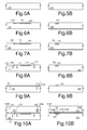
Figures 5A-10A, 11, 12 show cross-sections corresponding toFigure 3 , in successive manufacturing steps of the sensor ofFigure 2 ; -
Figures 5B-10B show cross-sections corresponding toFigure 4 , for the same manufacturing steps asFigures 5A-10A; -
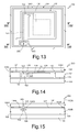
Figure 13 is a top plan view, with ghost parts, of a different embodiment of the present pressure sensor; -
Figure 14 is a cross-section of the pressure sensor ofFigure 13 , taken along section plane XIV-XIV; -
Figure 15 is a cross-section of the pressure sensor ofFigure 13 , taken along the section plane XV-XV; and -
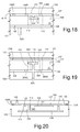
Figures 16-20 show details in cross-section of variants of the present pressure sensor. -
Figures 2-4 illustrate an embodiment of apressure sensor 100 made according to MEMS technology. Thepressure sensor 100 here comprises asensor region 101 having afirst face 101A and asecond face 101B. Thepressure sensor 100 further comprises afirst cap region 102 facing thefirst face 101A of thesensor region 101 and asecond cap region 103 facing thesecond face 101B of thesensor region 101. Thefirst cap region 102 is bonded to thefirst face 101A of thesensor region 101 by afirst bonding structure 104, and thesecond cap region 103 is bonded to thesecond face 101B of thesensor region 101 by asecond bonding structure 105. Thefirst bonding structure 104 is here formed by aperimetral region 106A and by a sealingregion 106B, which here in part coincide but could be completely distinct. Theperimetral region 106A and sealingregion 106B have a closed shape, for the reasons explained hereinafter, and also form spacers. Thebonding structures - A
first air gap 107 extends between thefirst face 101A of thesensor region 101 and thefirst cap region 102 there extends, and asecond air gap 108 extends between thesecond face 101B of thesensor region 101 and thesecond cap region 103. - A
trench 110 extends within thesensor region 101, between thefirst air gap 107 and thesecond air gap 108, fluidically connecting them. Thetrench 110 has a square spiral shape with five sides and delimits a supportingportion 120 external thereto, asensitive portion 121 inside it, and aspring portion 122 that connects the supportingportion 120 to thesensitive portion 121. In this way, thesensitive portion 121 is accommodated in a chamber formed by thefirst air gap 107, thesecond air gap 108 and thetrench 110 and is free to move, being mechanically uncoupled from the supportingportion 120. - The
sensitive portion 121 forms amembrane 111 delimited at the bottom by a buriedcavity 109. Themembrane 111 is here comprised between the buriedcavity 109 and thefirst air gap 107 and faces thefirst cap region 102. - As illustrated in the sections of
Figures 3-4 , and, with a dashed line, in the top plan view ofFigure 2 (where, for clarity, thefirst cap region 102 is illustrated as a ghost region), achannel 123 extends within thespring region 122, between the buriedcavity 109 and a well 112 formed in the supportingregion 120. In turn, the well 112 is connected to thefirst air gap 107 by anopening 124, extending through thesensor region 101 between thefirst face 101A of thesensor region 101 and the well 112 (see, in particularFigure 4 ). As may be noted fromFigures 2 and 4 , the sealingregion 106B extends above the well 112 and surrounds theopening 124, delimiting achamber 126 that is thus in communication with the well 112 and isolated from thefirst air gap 107 by the sealingregion 106B. - The buried
cavity 109, thechannel 123, and the well 112 are formed on a same level, underneath thefirst face 101A of thesensor region 101, have approximately the same height and are obtained simultaneously, as explained in detail hereinafter. - As shown in
Figures 2 and 3 , thefirst cap region 102, which has anouter face 102A and aninner face 102B, has at least one communication hole, here twocommunication holes 125, which extend between theouter face 102A and theinner face 102B of thefirst cap region 102. The communication holes 125 fluidically connect thefirst air gap 107 to the environment external to thepressure sensor 100 and thus expose themembrane 111 to the external pressure, enabling detection thereof, in a per se known manner. - A
getter region 128 extends on theinner face 102B of thefirst cap region 102, facing thechamber 126. Thegetter region 128 is formed by a thin layer of metal, for example barium, indium, magnesium, calcium, or sodium, having the aim of trapping possible residual gases released during bonding thefirst cap region 102 to thesensor region 101. - Hereinafter, the present manufacturing method will be described to form a single sensitive structure, where it is understood that this structure is replicated a number of times in a wafer, prior to dicing, in a per se known manner to a person skilled in the art.
- The
pressure sensor 100 ofFigure 2 is manufactured starting from afirst wafer 130, shown inFigures 5A-5B , of semiconductor material, for example monocrystalline silicon. As shown inFigures 6A-6B , the buriedcavity 109, thechannel 123, and the well 112 are formed in thefirst wafer 130, for example using the manufacturing process described inEP1577656 (corresponding to theUS 8,173,513 ). This process comprises forming a plurality of trenches, of appropriate depth, shape, and width, followed by an epitaxial growth in reducing environment. In this way, a silicon layer grows on thefirst wafer 130, closing the trenches at the top and forming themembrane 111. Then, thermal annealing is carried out, which causes migration of silicon atoms that tend to move into a position of lower energy. In this way, the buriedcavity 109, thechannel 123, and the well 112 are formed, all buried and covered by a silicon layer that also forms themembrane 111. If provided, a further epitaxial growth is then carried out, until a desired thickness is reached for themembrane 111. - Next (
Figures 7A-7B ), via a masking and etching step, theopening 124 is formed and fluidically connects the buriedcavity 109 to the outside of thefirst wafer 130 through the well 112 and thechannel 123. - Then (
Figures 8A, 8B ), using a masking layer (not illustrated), a deep silicon etch is carried out in thefirst wafer 130, thus forming thetrench 110, here still blind, external to and surrounding the buriedcavity 109. According to an alternative embodiment, the step ofFigure 8 may be carried out prior to the steps ofFigures 7A and 7B , i.e., it is possible to form first thetrench 110 and then theopening 124, using a non-liquid resist, for example a roller type, as mask for theopening 124. - Next (
Figures 9A, 9B ), asecond wafer 131 of semiconductor material, for example monocrystalline silicon, is etched for forming the communication holes 125, which are here still blind. Furthermore, thegetter regions 128 are formed on theface 131B of thesecond wafer 131 to be bonded to thefirst wafer 130, by depositing and defining a layer of suitable material. - As illustrated in
Figures 10A and 10B , thesecond wafer 131 is then flipped over and bonded to thefirst wafer 130, on the side of themembrane 111, by the first bonding structure 106. In this way, as mentioned, theperimetral region 106A delimits thefirst air gap 107, and the sealingregion 106B surrounds theopening 124 and defines thechamber 126, above theopening 124. - Bonding the
second wafer 131 to thefirst wafer 130 is made in vacuum so that the buriedcavity 109, thechannel 123, the well 112, theopening 124, and thechamber 126 remain in vacuum conditions. In this step, thegetter region 128 absorbs any possible residual gases due to bonding, further reducing the pressure in the buriedcavity 109. - Next (
Figure 11 ), thefirst wafer 130 and thesecond wafer 131 are thinned out. In particular, thinning of thefirst wafer 130 is carried out on the exposed side until reaching the bottom of thetrench 110, which thus becomes a through trench, and thinning of thesecond wafer 131 is carried out on the exposed side until reaching the bottom of the communication holes 125, which thus become through holes. In this way, thesensor region 101 and thefirst cap region 102 are formed; further, thetrench 110 extends throughout the thickness of thesensor region 101, and the communication holes 125 connect thefirst air gap 107 to the external environment. - A
third wafer 132 of semiconductor material, for example monocrystalline silicon, is then bonded to thesecond face 101B of thesensor region 101, as illustrated inFigure 12 , through thesecond bonding layer 105, thus defining thesecond air gap 108 between thesensor region 101 and thethird wafer 132. Thethird wafer 132 is then thinned out, thus forming thesecond cap region 103. - In this way, the gas trapped in the buried cavity 109 (as well as in the
channel 123 and in the well 112) during epitaxial growth may exit through theopening 124. Further, during bonding, performed in vacuum conditions, any possible gas that has remained is evacuated. The sealing region 106 maintains the vacuum within the buriedcavity 109 as well as in thechannel 123 and in the well 112 also subsequently, while thecommunication holes 125 fluidically connect thefirst air gap 107 with the external environment, enabling detection of the external pressure. In this way, the linearity of pressure detection improves considerably, thereby any possible compensation by the ASIC that processes the signal supplied by the pressure sensor becomes simpler and the testing time is reduced. - With the described pressure sensor, it is possible to reduce the thickness of the passivation that covers the
membrane 111. In this way, an increase of sensitivity is obtained. - According to a different embodiment,
Figures 13-15 , thefirst cap region 102 has acommunication hole 225, extending between theouter face 102A and theinner face 102B of thefirst cap region 102. Furthermore, no through holes connect thefirst air gap 107 or thesecond air gap 108 to the environment external to the pressure sensor. InFigures 13-15 , thecommunication hole 225 is here arranged above theopening 124 and the well 112 and connects the outside of the pressure sensor, here designated by 200, to thechamber 126 and to the buriedcavity 109. The latter is thus fluidically connected to the environment surrounding thepressure sensor 200. Instead, since no communication holes connect thefirst air gap 107 to the outside, the buriedcavity 109 is isolated from the surrounding environment by a sealingregion 106B. Consequently, in this embodiment, thefirst air gap 107 is in vacuum conditions as a result of the bonding of thesecond wafer 131. Themembrane 111 is thus also here exposed to the external pressure on a first side (the underside inFigure 14 ) and at an extremely low pressure (vacuum) on a second side (the upper side inFigure 14 ), and is thus able to work in a way similar to the embodiment ofFigures 2-4 . - In the embodiment of
Figures 13-15 , the getter region (designated by 228 inFigure 14 ) is arranged facing theair gap 107. - The
pressure sensor 200 ofFigures 13-15 is manufactured similarly to thepressure sensor 100 ofFigures 2-4 , except as regards perforation of the second wafer 131 (Figure 9 ). In fact, for thepressure sensor 200, a communication hole is formed, intended to be vertically aligned to thechamber 126 and to theopening 124, and thus within the area defined by the sealingregion 106B, instead of above thefirst air gap 107. - The
pressure sensor cavity 109 during formation thereof. In fact, in thepressure sensor 100 ofFigures 2-4 , the buriedcavity 109 is under vacuum, as explained above and thus the offset problem explained above is not present. - In the
pressure sensor 200 ofFigures 13-15 , instead, thecommunication hole 225 connects the external environment fluidically to the buriedcavity 109, whereas the sealing region 106 isolates thefirst air gap 107, which under vacuum. Also in this case, thus, no gases are trapped in a cavity in contact with themembrane 111, which might falsify reading of the external pressure. - Finally, it is clear that modifications and variations may be made to the device and to the manufacturing method described and illustrated herein, without thereby departing from the scope of the present invention, as defined in the attached claims.
- For instance,
Figures 16 and 17 show variants of thepressure sensor 100 ofFigures 2-4 . InFigures 16 and 17 , the opening that connects the buriedcavity 109, thechannel 123, and the well 112 to the outer surface of thesensor region 101 in order to create the vacuum during bonding of thefirst wafer 130, here designated by 324, extends between the well 112 and thesecond face 101B of thesensor region 101. Furthermore, the sealing region, here designated by 306B, is formed between thesensor region 101 and theinner face 103B of thesecond cap region 103, for example as part of thesecond sealing structure 105, and surrounds achamber 326, formed between thesensor region 101 and thesecond cap region 103. In this way, the vacuum in the buriedcavity 109 is set up during bonding of thethird wafer 132 to thefirst wafer 130. - Furthermore, as shown in
Figures 17 and18 , the communication holes that connect thefirst air gap 107 in thepressure sensor 100 may be formed in thesecond cap region 103, instead of in thefirst cap region 102. Here, one or more communication holes 325 (represented with dashed lines, in so far as they are not visible in the cross-section of these figures) extend between anouter face 103A and aninner face 103B of thesecond cap region 103 and connect themembrane 111 to the outside, since the trench 110 (which is also represented by a dashed line) connects together fluidically the first andsecond air gaps Figure 17 refers to an embodiment with anopening 324 extending between the well 112 and thesecond face 101B of thesensor region 101 and with a communication hole or holes 325, extending through thesecond cap region 103.Figure 18 refers to an embodiment with anopening 124 extending between the well 112 and thefirst face 101A of thesensor region 101 and with a communication hole or holes 325 extending through thesecond cap region 103. - Furthermore, the
sensor 200 ofFigures 13-15 may be modified so as to connect the buriedcavity 109 to the outside through thesecond cap region 103 through an opening 324 (extending between the well 112 and thesecond face 101B of the sensor region 101), a chamber 326 (formed between thesensor region 101 and the second cap region 103), and a communication hole 425 (in the second cap region 103), as illustrated in the detail ofFigure 19 . - The number of
communication holes - Finally, it is possible to form the second
monolithic cap region 103 together with thesensor region 101, forming thesecond air gap 108 with the same process used for the buriedcavity 109, before forming the latter, in the embodiments ofFigures 2-4, 13-15, and 18 . For instance,Figure 20 shows asingle substrate 500 forming thesensor region 101 and thesecond cap region 103. Here, theair gap 107 is connected to the outside, as in the embodiment ofFigures 3-5 . Similar variants are possible for the embodiments ofFigures 13-15 and 18 . - As an alternative and in a dual way, it is possible to form the first
monolithic cap region 102 together with thesensor region 101, forming thefirst air gap 107 with the process used for the buriedcavity 109, in the embodiments ofFigures 16, 17 , and19 . - In this way, the pressure sensor may be manufactured with a smaller number of wafers than currently, since the first or the
second air gap
Claims (18)
- A micro-electro-mechanical pressure sensor device (100), comprising:a first region (102; 103);a second region (101; 500) of semiconductor material having a first face (101A; 101B) and a second face (101B; 101A);the first region (102; 103) facing and fixed to the first face (101A; 101B) of the second region (101; 500);a first air gap (107; 108), extending between the first face (101A; 101B) of the second region (101; 500) and the first region (102; 103);a buried cavity (109), extending in the second region (101; 500);a membrane (111) within the second region (101; 500) between the buried cavity (109) and the first face (101A; 101B) or the second face (101B; 101A) of the second region (101; 500);a through trench (110), extending within the second region (101; 500) and laterally delimiting a sensitive portion (121) housing the membrane, a supporting portion (120) and a spring portion (122), the spring portion connecting the sensitive portion (121) to the supporting portion (120); anda channel (123), extending within the spring portion (122) and connecting the buried cavity (109) to the first face (101A; 101B) of the second region (101; 500); one between the buried cavity and the first air gap being fluidically connected to the outside of the device and another between the buried cavity and the first air gap being isolated from the outside.
- A device according to claim 1, comprising a sealing region (106B; 306B), extending between the first face (101A; 101B) of the second region (101; 500) and the first region (102; 103) and isolating the channel (123) from the first air gap (107; 108).
- A device according to claim 2, wherein the channel (123) extends at distance from the first face (101A; 101B) of the second region (101; 500), and an opening (124; 324) extends in the second region (101; 500) between the first face (101A; 101B) and the channel (123), the sealing region (106B; 306B) having a closed shape surrounding a chamber (126; 326), extending between the first and second regions (102; 103, 101) and connected to the opening (124; 324).
- A device according to claim 3, wherein the first region (102; 103) has an outer face (102A; 103A) and an inner face (102B; 103B), the inner face (102B; 103B) facing the second region (101; 500), and wherein at least one through hole (125; 325) extends between the inner face (102B; 103B) and the outer face (102A; 103A) of the first region (102; 103) outside the chamber (126; 326) and connects the first air gap (107; 108) with the outer face (102A; 103A) of the first region (102; 103).
- A device according to claim 3, further comprising a third region (102; 103) facing the second face (101A; 101B) of the second region (101) and a second air gap (107; 108), extending between the second face (101A; 101B) of the second region (101) and the third region (102; 103), wherein the third region (102; 103) has an outer face and an inner face, the inner face facing the second region (101), and wherein at least one through hole (125; 325) extends between the inner face and the outer face of the third region (102; 103) and ends at the second air gap (107; 108), connecting the second air gap (107; 108) with the outer face of the second region (102; 103).
- A device according to claim 3, wherein the first region (102; 103) has an outer face (102A; 103A) and an inner face (102B; 103B), the inner face facing the second region (101), and wherein a through hole (225; 425) extends between the outer face (102A; 103A) and the inner face (102B; 103B) of the first region (102; 103), inside the sealing region (106B), the first air gap (107; 108) being isolated from the through hole (225; 425) by the sealing region (106B; 306B).
- A device according to any of claims 2-6, wherein the first region (102; 103) and the second region (101; 500) are bonded together through a bonding structure (104; 105) including the sealing region (106B; 306B) and delimiting the first air gap (107; 108).
- A device according to any one of claims 1-4, and 6, further comprising a third region (102; 103) facing a second face (101A; 101B) of the second region (101) and a second air gap (107; 108), extending between the second face (101A; 101B) of the second region (101) and the third region (102; 103)
wherein the third region (102; 103) and the second region (101) are bonded together via a bonding layer (104; 105) delimiting the second air gap (107; 108). - A device according to any of claims 1-4, and 6, further comprising a third region (102; 103), of semiconductor material and monolithic with the second region (101), and a second air gap (107; 108), extending between the second region (101) and the third region (102; 103).
- A device according to any of the preceding claims, comprising a getter region (128; 228) formed on the first region (102; 103) facing the one between the buried cavity and the first air gap which is isolated from the outside.
- A process for manufacturing a micro-electro-mechanical type pressure sensor device (100), comprising:forming a second region (101; 500) of semiconductor material having a first face;forming a buried cavity (109) in the second region (101; 500), the buried cavity delimiting a membrane (111);forming, within the second region (101; 500), a trench (110), the trench delimiting a sensitive portion (121) accommodating the cavity, a supporting portion (120), and a spring portion (122) which connects the sensitive portion (121) to the supporting portion (120); andforming, within the spring portion (122), a channel (123), which connects the buried cavity (109) to the first face (101A; 101B) of the second region (101);bonding a first region (102; 103) to the first face (101A; 101B) of the second region (101) to form a first air gap (107; 108) above the buried cavity;
forming a fluidic path connecting one between the buried cavity and the first air gap to the outside of the device; and
forming a sealing structure fluidically isolating the other between the buried cavity and the first air gap from the outside of the device. - A process according to claim 11, wherein forming the buried cavity (109) and forming the channel (123) are carried out simultaneously.
- A process according to claim 11 or 12, wherein forming an isolating sealing structure comprises forming a sealing region (106B; 306B), extending between the first face (101A; 101B) of the second region (101; 500) and the first region (102; 103).
- A process according to claim 13, comprising forming at least one opening (124; 324) in the second region (101; 500) between the first face (101A; 101B) and the channel (123), the sealing region (106B; 306B) having a closed shape surrounding the opening (124).
- A process according to claim 14, wherein forming a fluidic path comprises forming at least one through hole (125; 325) in the first region (102; 103), outside the sealing region (106B) and in fluidic connection with the first air gap (107; 108).
- A process according to claim 14, wherein forming a fluidic path comprises forming a through hole (225; 425) in the first region (102; 103), inside the sealing region (106B) and in fluidic connection with the channel and the buried cavity.
- A process according to any of claims 14-16, wherein forming a sealing structure comprises simultaneously forming a bonding region delimiting the first air gap.
- A process according to any of claims 14-17, comprising bonding a third region (102; 103) to a second face (101A; 101B) of the second region (101), thereby forming a second air gap (107; 108) between the second face (101A; 101B) of the second region (101) and the third region (102; 103), wherein bonding the third region (102; 103) comprises forming a bonding layer (104; 105) delimiting the second air gap (107; 108).
Applications Claiming Priority (1)
| Application Number | Priority Date | Filing Date | Title |
|---|---|---|---|
| ITUB2016A001080A ITUB20161080A1 (en) | 2016-02-25 | 2016-02-25 | PRESSURE SENSOR DEVICE OF MICRO-ELECTRO-MECHANICAL TYPE WITH REDUCED TEMPERATURE SENSITIVITY |
Publications (2)
| Publication Number | Publication Date |
|---|---|
| EP3210934A1 true EP3210934A1 (en) | 2017-08-30 |
| EP3210934B1 EP3210934B1 (en) | 2020-06-17 |
Family
ID=55949001
Family Applications (1)
| Application Number | Title | Priority Date | Filing Date |
|---|---|---|---|
| EP16194672.8A Active EP3210934B1 (en) | 2016-02-25 | 2016-10-19 | Micro-electro-mechanical type pressure device having low sensitivity to temperature |
Country Status (4)
| Country | Link |
|---|---|
| US (1) | US9975756B2 (en) |
| EP (1) | EP3210934B1 (en) |
| CN (2) | CN107117577B (en) |
| IT (1) | ITUB20161080A1 (en) |
Cited By (2)
| Publication number | Priority date | Publication date | Assignee | Title |
|---|---|---|---|---|
| US20190031501A1 (en) * | 2017-07-28 | 2019-01-31 | Advanced Semiconductor Engineering Korea, Inc. | Microelectromechanical systems and method of manufacturing the same |
| IT202300022215A1 (en) * | 2023-10-24 | 2025-04-24 | St Microelectronics Int Nv | PRESSURE SENSOR WITH IMPROVED REJECTION OF UNWANTED STIMULI |
Families Citing this family (10)
| Publication number | Priority date | Publication date | Assignee | Title |
|---|---|---|---|---|
| ITUB20161080A1 (en) * | 2016-02-25 | 2017-08-25 | St Microelectronics Srl | PRESSURE SENSOR DEVICE OF MICRO-ELECTRO-MECHANICAL TYPE WITH REDUCED TEMPERATURE SENSITIVITY |
| DE102017203384B3 (en) * | 2017-03-02 | 2018-01-18 | Robert Bosch Gmbh | Micromechanical pressure sensor |
| CN107894297B (en) * | 2017-11-07 | 2020-02-18 | 无锡必创传感科技有限公司 | Pressure sensor chip and manufacturing method thereof |
| US11274035B2 (en) | 2019-04-24 | 2022-03-15 | X-Celeprint Limited | Overhanging device structures and related methods of manufacture |
| US12162747B2 (en) | 2018-12-03 | 2024-12-10 | X-Celeprint Limited | Enclosed cavity structures |
| US11981560B2 (en) * | 2020-06-09 | 2024-05-14 | Analog Devices, Inc. | Stress-isolated MEMS device comprising substrate having cavity and method of manufacture |
| CN115702331B (en) * | 2020-06-24 | 2025-03-28 | 株式会社村田制作所 | Pressure Sensors |
| US12515942B2 (en) * | 2021-06-25 | 2026-01-06 | Stmicroelectronics S.R.L. | MEMS device comprising an insulated suspended diaphragm, in particular pressure sensor, and manufacturing process thereof |
| CN117836598A (en) * | 2021-08-31 | 2024-04-05 | 株式会社村田制作所 | Pressure sensor element and pressure sensor |
| IT202300025878A1 (en) * | 2023-12-04 | 2025-06-04 | St Microelectronics Int Nv | SEALED MEMBRANE MICROELECTROMECHANICAL DEVICE |
Citations (3)
| Publication number | Priority date | Publication date | Assignee | Title |
|---|---|---|---|---|
| EP1577656A1 (en) | 2004-03-19 | 2005-09-21 | STMicroelectronics S.r.l. | Method for manufacturing a semiconductor pressure sensor |
| WO2007042336A2 (en) * | 2005-10-14 | 2007-04-19 | Stmicroelectronics S.R.L. | Substrate-level assembly for an integrated device, manufacturing process thereof and related integrated device |
| US20150001651A1 (en) * | 2013-06-28 | 2015-01-01 | Stmicroelectronics S.R.I. | Mems device having a suspended diaphragm and manufacturing process thereof |
Family Cites Families (15)
| Publication number | Priority date | Publication date | Assignee | Title |
|---|---|---|---|---|
| EP1808046B1 (en) * | 2004-10-27 | 2010-09-22 | Epcos Ag | Reduction of air damping in mems device |
| EP2159558A1 (en) * | 2008-08-28 | 2010-03-03 | Sensirion AG | A method for manufacturing an integrated pressure sensor |
| ITTO20090616A1 (en) * | 2009-08-05 | 2011-02-06 | St Microelectronics Srl | PROCESS OF MANUFACTURING OF MEMS DEVICES EQUIPPED WITH CUTTED CAVITIES AND MEMS DEVICE SO OBTAINED |
| BR112012009300A2 (en) * | 2009-10-21 | 2020-08-18 | Biocartis Sa | microfluidic cartridge, pneumatic interface plate, fluid drive system within a microfluidic cartridge, and pneumatic instrument. |
| WO2013133899A1 (en) * | 2012-03-08 | 2013-09-12 | Cyvek, Inc | Microfluidic assay systems employing micro-particles and methods of manufacture |
| US8217474B2 (en) * | 2009-12-28 | 2012-07-10 | Solid State System Co., Ltd. | Hermetic MEMS device and method for fabricating hermetic MEMS device and package structure of MEMS device |
| FR2994228B1 (en) * | 2012-07-31 | 2017-05-12 | Commissariat Energie Atomique | PUMP REALIZED IN A SUBSTRATE |
| ITTO20130539A1 (en) * | 2013-06-28 | 2014-12-29 | Stmicroelectronics International N V | MEMS DEVICE INCORPORATING A FLUID AND RELATIVE PATH OF MANUFACTURING PROCEDURE |
| US9114976B1 (en) * | 2014-03-07 | 2015-08-25 | Taiwan Semiconductor Manufacturing Company Limited | Semiconductor arrangement with stress release configuration |
| WO2015163181A1 (en) * | 2014-04-25 | 2015-10-29 | 日立オートモティブシステムズ株式会社 | Cooling control device, flow rate control valve and cooling control method |
| CN104062059B (en) * | 2014-06-13 | 2017-12-01 | 江苏英特神斯科技有限公司 | A kind of MEMS piezoresistive pressure sensor and its manufacture method |
| CN205262665U (en) * | 2015-06-22 | 2016-05-25 | 意法半导体股份有限公司 | Pressure sensor |
| ITUB20155716A1 (en) * | 2015-11-19 | 2017-05-19 | St Microelectronics Srl | MICRO-ELECTRO-MECHANICAL DEVICE EQUIPPED WITH TWO CAVITIES AND RELATIVE PROCESS OF MANUFACTURE |
| US9670057B1 (en) * | 2016-01-29 | 2017-06-06 | Infineon Technologies Ag | Sensor device and method for making thereof |
| ITUB20161080A1 (en) * | 2016-02-25 | 2017-08-25 | St Microelectronics Srl | PRESSURE SENSOR DEVICE OF MICRO-ELECTRO-MECHANICAL TYPE WITH REDUCED TEMPERATURE SENSITIVITY |
-
2016
- 2016-02-25 IT ITUB2016A001080A patent/ITUB20161080A1/en unknown
- 2016-09-26 US US15/276,613 patent/US9975756B2/en active Active
- 2016-09-30 CN CN201611035493.8A patent/CN107117577B/en active Active
- 2016-09-30 CN CN201621255067.0U patent/CN206872419U/en not_active Withdrawn - After Issue
- 2016-10-19 EP EP16194672.8A patent/EP3210934B1/en active Active
Patent Citations (4)
| Publication number | Priority date | Publication date | Assignee | Title |
|---|---|---|---|---|
| EP1577656A1 (en) | 2004-03-19 | 2005-09-21 | STMicroelectronics S.r.l. | Method for manufacturing a semiconductor pressure sensor |
| US8173513B2 (en) | 2004-03-19 | 2012-05-08 | Stmicroelectronics S.R.L. | Method for manufacturing a semiconductor pressure sensor |
| WO2007042336A2 (en) * | 2005-10-14 | 2007-04-19 | Stmicroelectronics S.R.L. | Substrate-level assembly for an integrated device, manufacturing process thereof and related integrated device |
| US20150001651A1 (en) * | 2013-06-28 | 2015-01-01 | Stmicroelectronics S.R.I. | Mems device having a suspended diaphragm and manufacturing process thereof |
Cited By (4)
| Publication number | Priority date | Publication date | Assignee | Title |
|---|---|---|---|---|
| US20190031501A1 (en) * | 2017-07-28 | 2019-01-31 | Advanced Semiconductor Engineering Korea, Inc. | Microelectromechanical systems and method of manufacturing the same |
| US10407298B2 (en) * | 2017-07-28 | 2019-09-10 | Advanced Semiconductor Engineering Korea, Inc. | Microelectromechanical systems and method of manufacturing the same |
| IT202300022215A1 (en) * | 2023-10-24 | 2025-04-24 | St Microelectronics Int Nv | PRESSURE SENSOR WITH IMPROVED REJECTION OF UNWANTED STIMULI |
| EP4545927A1 (en) | 2023-10-24 | 2025-04-30 | STMicroelectronics International N.V. | Pressure sensor having improved rejection of undesired stimuli |
Also Published As
| Publication number | Publication date |
|---|---|
| CN107117577A (en) | 2017-09-01 |
| US9975756B2 (en) | 2018-05-22 |
| CN206872419U (en) | 2018-01-12 |
| US20170247249A1 (en) | 2017-08-31 |
| CN107117577B (en) | 2019-12-31 |
| ITUB20161080A1 (en) | 2017-08-25 |
| EP3210934B1 (en) | 2020-06-17 |
Similar Documents
| Publication | Publication Date | Title |
|---|---|---|
| EP3210934B1 (en) | Micro-electro-mechanical type pressure device having low sensitivity to temperature | |
| US10626008B2 (en) | Micro-electro-mechanical device and manufacturing process thereof | |
| JP4858547B2 (en) | Semiconductor device and manufacturing method thereof | |
| US9926188B2 (en) | Sensor unit including a decoupling structure and manufacturing method therefor | |
| CN107265395B (en) | Method for manufacturing a MEMS pressure sensor and corresponding MEMS pressure sensor | |
| US8748998B2 (en) | Sensor module | |
| EP2871455B1 (en) | Pressure sensor | |
| JP5649474B2 (en) | Capacitance type pressure sensor and method of manufacturing capacitance type pressure sensor | |
| EP3326964B1 (en) | Semiconductor integrated device with electrical contacts between stacked dies and corresponding manufacturing process | |
| JP5913564B2 (en) | Electrodes defined by out-of-plane spacers | |
| CN105874312B (en) | Inertia and pressure sensor on a single chip | |
| EP3052901B1 (en) | Inertial and pressure sensors on single chip | |
| US20150001651A1 (en) | Mems device having a suspended diaphragm and manufacturing process thereof | |
| JP5605347B2 (en) | Manufacturing method of semiconductor device | |
| US11358862B2 (en) | Micro-electro-mechanical device having two buried cavities and manufacturing process thereof | |
| TWI652728B (en) | Epi-poly etch stop for out of plane spacer defined electrode | |
| US11027967B2 (en) | Deformable membrane and a compensating structure thereof | |
| US9302906B2 (en) | Capacitive pressure sensor and method | |
| US11915924B2 (en) | Semiconductor device and method for manufacturing the same | |
| US20250276893A1 (en) | Microelectromechanical sensor with improved external fluidic coupling and manufacturing process thereof |
Legal Events
| Date | Code | Title | Description |
|---|---|---|---|
| PUAI | Public reference made under article 153(3) epc to a published international application that has entered the european phase |
Free format text: ORIGINAL CODE: 0009012 |
|
| STAA | Information on the status of an ep patent application or granted ep patent |
Free format text: STATUS: THE APPLICATION HAS BEEN PUBLISHED |
|
| AK | Designated contracting states |
Kind code of ref document: A1 Designated state(s): AL AT BE BG CH CY CZ DE DK EE ES FI FR GB GR HR HU IE IS IT LI LT LU LV MC MK MT NL NO PL PT RO RS SE SI SK SM TR |
|
| AX | Request for extension of the european patent |
Extension state: BA ME |
|
| STAA | Information on the status of an ep patent application or granted ep patent |
Free format text: STATUS: REQUEST FOR EXAMINATION WAS MADE |
|
| 17P | Request for examination filed |
Effective date: 20180228 |
|
| RBV | Designated contracting states (corrected) |
Designated state(s): AL AT BE BG CH CY CZ DE DK EE ES FI FR GB GR HR HU IE IS IT LI LT LU LV MC MK MT NL NO PL PT RO RS SE SI SK SM TR |
|
| REG | Reference to a national code |
Ref country code: DE Ref legal event code: R079 Ref document number: 602016038137 Country of ref document: DE Free format text: PREVIOUS MAIN CLASS: B81B0003000000 Ipc: G01L0019040000 |
|
| GRAP | Despatch of communication of intention to grant a patent |
Free format text: ORIGINAL CODE: EPIDOSNIGR1 |
|
| STAA | Information on the status of an ep patent application or granted ep patent |
Free format text: STATUS: GRANT OF PATENT IS INTENDED |
|
| RIC1 | Information provided on ipc code assigned before grant |
Ipc: B81B 7/00 20060101AFI20191205BHEP |
|
| RIC1 | Information provided on ipc code assigned before grant |
Ipc: G01L 19/04 20060101AFI20191209BHEP Ipc: B81B 7/00 20060101ALI20191209BHEP Ipc: G01L 19/14 20060101ALI20191209BHEP |
|
| INTG | Intention to grant announced |
Effective date: 20200103 |
|
| GRAS | Grant fee paid |
Free format text: ORIGINAL CODE: EPIDOSNIGR3 |
|
| GRAA | (expected) grant |
Free format text: ORIGINAL CODE: 0009210 |
|
| STAA | Information on the status of an ep patent application or granted ep patent |
Free format text: STATUS: THE PATENT HAS BEEN GRANTED |
|
| AK | Designated contracting states |
Kind code of ref document: B1 Designated state(s): AL AT BE BG CH CY CZ DE DK EE ES FI FR GB GR HR HU IE IS IT LI LT LU LV MC MK MT NL NO PL PT RO RS SE SI SK SM TR |
|
| REG | Reference to a national code |
Ref country code: GB Ref legal event code: FG4D |
|
| REG | Reference to a national code |
Ref country code: CH Ref legal event code: EP |
|
| REG | Reference to a national code |
Ref country code: IE Ref legal event code: FG4D |
|
| REG | Reference to a national code |
Ref country code: DE Ref legal event code: R096 Ref document number: 602016038137 Country of ref document: DE |
|
| REG | Reference to a national code |
Ref country code: AT Ref legal event code: REF Ref document number: 1281893 Country of ref document: AT Kind code of ref document: T Effective date: 20200715 |
|
| PG25 | Lapsed in a contracting state [announced via postgrant information from national office to epo] |
Ref country code: GR Free format text: LAPSE BECAUSE OF FAILURE TO SUBMIT A TRANSLATION OF THE DESCRIPTION OR TO PAY THE FEE WITHIN THE PRESCRIBED TIME-LIMIT Effective date: 20200918 Ref country code: NO Free format text: LAPSE BECAUSE OF FAILURE TO SUBMIT A TRANSLATION OF THE DESCRIPTION OR TO PAY THE FEE WITHIN THE PRESCRIBED TIME-LIMIT Effective date: 20200917 Ref country code: FI Free format text: LAPSE BECAUSE OF FAILURE TO SUBMIT A TRANSLATION OF THE DESCRIPTION OR TO PAY THE FEE WITHIN THE PRESCRIBED TIME-LIMIT Effective date: 20200617 Ref country code: LT Free format text: LAPSE BECAUSE OF FAILURE TO SUBMIT A TRANSLATION OF THE DESCRIPTION OR TO PAY THE FEE WITHIN THE PRESCRIBED TIME-LIMIT Effective date: 20200617 Ref country code: SE Free format text: LAPSE BECAUSE OF FAILURE TO SUBMIT A TRANSLATION OF THE DESCRIPTION OR TO PAY THE FEE WITHIN THE PRESCRIBED TIME-LIMIT Effective date: 20200617 |
|
| REG | Reference to a national code |
Ref country code: LT Ref legal event code: MG4D |
|
| REG | Reference to a national code |
Ref country code: NL Ref legal event code: MP Effective date: 20200617 |
|
| PG25 | Lapsed in a contracting state [announced via postgrant information from national office to epo] |
Ref country code: BG Free format text: LAPSE BECAUSE OF FAILURE TO SUBMIT A TRANSLATION OF THE DESCRIPTION OR TO PAY THE FEE WITHIN THE PRESCRIBED TIME-LIMIT Effective date: 20200917 Ref country code: HR Free format text: LAPSE BECAUSE OF FAILURE TO SUBMIT A TRANSLATION OF THE DESCRIPTION OR TO PAY THE FEE WITHIN THE PRESCRIBED TIME-LIMIT Effective date: 20200617 Ref country code: RS Free format text: LAPSE BECAUSE OF FAILURE TO SUBMIT A TRANSLATION OF THE DESCRIPTION OR TO PAY THE FEE WITHIN THE PRESCRIBED TIME-LIMIT Effective date: 20200617 Ref country code: LV Free format text: LAPSE BECAUSE OF FAILURE TO SUBMIT A TRANSLATION OF THE DESCRIPTION OR TO PAY THE FEE WITHIN THE PRESCRIBED TIME-LIMIT Effective date: 20200617 |
|
| REG | Reference to a national code |
Ref country code: AT Ref legal event code: MK05 Ref document number: 1281893 Country of ref document: AT Kind code of ref document: T Effective date: 20200617 |
|
| PG25 | Lapsed in a contracting state [announced via postgrant information from national office to epo] |
Ref country code: AL Free format text: LAPSE BECAUSE OF FAILURE TO SUBMIT A TRANSLATION OF THE DESCRIPTION OR TO PAY THE FEE WITHIN THE PRESCRIBED TIME-LIMIT Effective date: 20200617 Ref country code: NL Free format text: LAPSE BECAUSE OF FAILURE TO SUBMIT A TRANSLATION OF THE DESCRIPTION OR TO PAY THE FEE WITHIN THE PRESCRIBED TIME-LIMIT Effective date: 20200617 |
|
| PG25 | Lapsed in a contracting state [announced via postgrant information from national office to epo] |
Ref country code: ES Free format text: LAPSE BECAUSE OF FAILURE TO SUBMIT A TRANSLATION OF THE DESCRIPTION OR TO PAY THE FEE WITHIN THE PRESCRIBED TIME-LIMIT Effective date: 20200617 Ref country code: PT Free format text: LAPSE BECAUSE OF FAILURE TO SUBMIT A TRANSLATION OF THE DESCRIPTION OR TO PAY THE FEE WITHIN THE PRESCRIBED TIME-LIMIT Effective date: 20201019 Ref country code: AT Free format text: LAPSE BECAUSE OF FAILURE TO SUBMIT A TRANSLATION OF THE DESCRIPTION OR TO PAY THE FEE WITHIN THE PRESCRIBED TIME-LIMIT Effective date: 20200617 Ref country code: RO Free format text: LAPSE BECAUSE OF FAILURE TO SUBMIT A TRANSLATION OF THE DESCRIPTION OR TO PAY THE FEE WITHIN THE PRESCRIBED TIME-LIMIT Effective date: 20200617 Ref country code: CZ Free format text: LAPSE BECAUSE OF FAILURE TO SUBMIT A TRANSLATION OF THE DESCRIPTION OR TO PAY THE FEE WITHIN THE PRESCRIBED TIME-LIMIT Effective date: 20200617 Ref country code: IT Free format text: LAPSE BECAUSE OF FAILURE TO SUBMIT A TRANSLATION OF THE DESCRIPTION OR TO PAY THE FEE WITHIN THE PRESCRIBED TIME-LIMIT Effective date: 20200617 Ref country code: EE Free format text: LAPSE BECAUSE OF FAILURE TO SUBMIT A TRANSLATION OF THE DESCRIPTION OR TO PAY THE FEE WITHIN THE PRESCRIBED TIME-LIMIT Effective date: 20200617 Ref country code: SM Free format text: LAPSE BECAUSE OF FAILURE TO SUBMIT A TRANSLATION OF THE DESCRIPTION OR TO PAY THE FEE WITHIN THE PRESCRIBED TIME-LIMIT Effective date: 20200617 |
|
| PG25 | Lapsed in a contracting state [announced via postgrant information from national office to epo] |
Ref country code: PL Free format text: LAPSE BECAUSE OF FAILURE TO SUBMIT A TRANSLATION OF THE DESCRIPTION OR TO PAY THE FEE WITHIN THE PRESCRIBED TIME-LIMIT Effective date: 20200617 Ref country code: SK Free format text: LAPSE BECAUSE OF FAILURE TO SUBMIT A TRANSLATION OF THE DESCRIPTION OR TO PAY THE FEE WITHIN THE PRESCRIBED TIME-LIMIT Effective date: 20200617 Ref country code: IS Free format text: LAPSE BECAUSE OF FAILURE TO SUBMIT A TRANSLATION OF THE DESCRIPTION OR TO PAY THE FEE WITHIN THE PRESCRIBED TIME-LIMIT Effective date: 20201017 |
|
| REG | Reference to a national code |
Ref country code: DE Ref legal event code: R097 Ref document number: 602016038137 Country of ref document: DE |
|
| PLBE | No opposition filed within time limit |
Free format text: ORIGINAL CODE: 0009261 |
|
| STAA | Information on the status of an ep patent application or granted ep patent |
Free format text: STATUS: NO OPPOSITION FILED WITHIN TIME LIMIT |
|
| PG25 | Lapsed in a contracting state [announced via postgrant information from national office to epo] |
Ref country code: DK Free format text: LAPSE BECAUSE OF FAILURE TO SUBMIT A TRANSLATION OF THE DESCRIPTION OR TO PAY THE FEE WITHIN THE PRESCRIBED TIME-LIMIT Effective date: 20200617 |
|
| 26N | No opposition filed |
Effective date: 20210318 |
|
| PG25 | Lapsed in a contracting state [announced via postgrant information from national office to epo] |
Ref country code: SI Free format text: LAPSE BECAUSE OF FAILURE TO SUBMIT A TRANSLATION OF THE DESCRIPTION OR TO PAY THE FEE WITHIN THE PRESCRIBED TIME-LIMIT Effective date: 20200617 |
|
| REG | Reference to a national code |
Ref country code: CH Ref legal event code: PL |
|
| GBPC | Gb: european patent ceased through non-payment of renewal fee |
Effective date: 20201019 |
|
| PG25 | Lapsed in a contracting state [announced via postgrant information from national office to epo] |
Ref country code: MC Free format text: LAPSE BECAUSE OF FAILURE TO SUBMIT A TRANSLATION OF THE DESCRIPTION OR TO PAY THE FEE WITHIN THE PRESCRIBED TIME-LIMIT Effective date: 20200617 Ref country code: LU Free format text: LAPSE BECAUSE OF NON-PAYMENT OF DUE FEES Effective date: 20201019 |
|
| REG | Reference to a national code |
Ref country code: BE Ref legal event code: MM Effective date: 20201031 |
|
| PG25 | Lapsed in a contracting state [announced via postgrant information from national office to epo] |
Ref country code: FR Free format text: LAPSE BECAUSE OF NON-PAYMENT OF DUE FEES Effective date: 20201031 |
|
| PG25 | Lapsed in a contracting state [announced via postgrant information from national office to epo] |
Ref country code: BE Free format text: LAPSE BECAUSE OF NON-PAYMENT OF DUE FEES Effective date: 20201031 Ref country code: CH Free format text: LAPSE BECAUSE OF NON-PAYMENT OF DUE FEES Effective date: 20201031 Ref country code: LI Free format text: LAPSE BECAUSE OF NON-PAYMENT OF DUE FEES Effective date: 20201031 Ref country code: GB Free format text: LAPSE BECAUSE OF NON-PAYMENT OF DUE FEES Effective date: 20201019 |
|
| PG25 | Lapsed in a contracting state [announced via postgrant information from national office to epo] |
Ref country code: IE Free format text: LAPSE BECAUSE OF NON-PAYMENT OF DUE FEES Effective date: 20201019 |
|
| PG25 | Lapsed in a contracting state [announced via postgrant information from national office to epo] |
Ref country code: TR Free format text: LAPSE BECAUSE OF FAILURE TO SUBMIT A TRANSLATION OF THE DESCRIPTION OR TO PAY THE FEE WITHIN THE PRESCRIBED TIME-LIMIT Effective date: 20200617 Ref country code: MT Free format text: LAPSE BECAUSE OF FAILURE TO SUBMIT A TRANSLATION OF THE DESCRIPTION OR TO PAY THE FEE WITHIN THE PRESCRIBED TIME-LIMIT Effective date: 20200617 Ref country code: CY Free format text: LAPSE BECAUSE OF FAILURE TO SUBMIT A TRANSLATION OF THE DESCRIPTION OR TO PAY THE FEE WITHIN THE PRESCRIBED TIME-LIMIT Effective date: 20200617 |
|
| PG25 | Lapsed in a contracting state [announced via postgrant information from national office to epo] |
Ref country code: MK Free format text: LAPSE BECAUSE OF FAILURE TO SUBMIT A TRANSLATION OF THE DESCRIPTION OR TO PAY THE FEE WITHIN THE PRESCRIBED TIME-LIMIT Effective date: 20200617 |
|
| PGFP | Annual fee paid to national office [announced via postgrant information from national office to epo] |
Ref country code: DE Payment date: 20250923 Year of fee payment: 10 |