EP3208836A1 - A method to improve hci performance for finfet - Google Patents
A method to improve hci performance for finfet Download PDFInfo
- Publication number
- EP3208836A1 EP3208836A1 EP17155783.8A EP17155783A EP3208836A1 EP 3208836 A1 EP3208836 A1 EP 3208836A1 EP 17155783 A EP17155783 A EP 17155783A EP 3208836 A1 EP3208836 A1 EP 3208836A1
- Authority
- EP
- European Patent Office
- Prior art keywords
- fins
- layer
- gate
- semiconductor
- substrate
- Prior art date
- Legal status (The legal status is an assumption and is not a legal conclusion. Google has not performed a legal analysis and makes no representation as to the accuracy of the status listed.)
- Granted
Links
Images



Classifications
-
- H—ELECTRICITY
- H10—SEMICONDUCTOR DEVICES; ELECTRIC SOLID-STATE DEVICES NOT OTHERWISE PROVIDED FOR
- H10D—INORGANIC ELECTRIC SEMICONDUCTOR DEVICES
- H10D30/00—Field-effect transistors [FET]
- H10D30/01—Manufacture or treatment
- H10D30/021—Manufacture or treatment of FETs having insulated gates [IGFET]
- H10D30/024—Manufacture or treatment of FETs having insulated gates [IGFET] of fin field-effect transistors [FinFET]
-
- H—ELECTRICITY
- H10—SEMICONDUCTOR DEVICES; ELECTRIC SOLID-STATE DEVICES NOT OTHERWISE PROVIDED FOR
- H10D—INORGANIC ELECTRIC SEMICONDUCTOR DEVICES
- H10D30/00—Field-effect transistors [FET]
- H10D30/60—Insulated-gate field-effect transistors [IGFET]
- H10D30/62—Fin field-effect transistors [FinFET]
-
- H—ELECTRICITY
- H10—SEMICONDUCTOR DEVICES; ELECTRIC SOLID-STATE DEVICES NOT OTHERWISE PROVIDED FOR
- H10D—INORGANIC ELECTRIC SEMICONDUCTOR DEVICES
- H10D30/00—Field-effect transistors [FET]
- H10D30/60—Insulated-gate field-effect transistors [IGFET]
- H10D30/791—Arrangements for exerting mechanical stress on the crystal lattice of the channel regions
- H10D30/797—Arrangements for exerting mechanical stress on the crystal lattice of the channel regions being in source or drain regions, e.g. SiGe source or drain
-
- H—ELECTRICITY
- H10—SEMICONDUCTOR DEVICES; ELECTRIC SOLID-STATE DEVICES NOT OTHERWISE PROVIDED FOR
- H10D—INORGANIC ELECTRIC SEMICONDUCTOR DEVICES
- H10D62/00—Semiconductor bodies, or regions thereof, of devices having potential barriers
- H10D62/10—Shapes, relative sizes or dispositions of the regions of the semiconductor bodies; Shapes of the semiconductor bodies
- H10D62/13—Semiconductor regions connected to electrodes carrying current to be rectified, amplified or switched, e.g. source or drain regions
- H10D62/149—Source or drain regions of field-effect devices
- H10D62/151—Source or drain regions of field-effect devices of IGFETs
-
- H—ELECTRICITY
- H10—SEMICONDUCTOR DEVICES; ELECTRIC SOLID-STATE DEVICES NOT OTHERWISE PROVIDED FOR
- H10D—INORGANIC ELECTRIC SEMICONDUCTOR DEVICES
- H10D62/00—Semiconductor bodies, or regions thereof, of devices having potential barriers
- H10D62/10—Shapes, relative sizes or dispositions of the regions of the semiconductor bodies; Shapes of the semiconductor bodies
- H10D62/17—Semiconductor regions connected to electrodes not carrying current to be rectified, amplified or switched, e.g. channel regions
- H10D62/213—Channel regions of field-effect devices
- H10D62/221—Channel regions of field-effect devices of FETs
- H10D62/235—Channel regions of field-effect devices of FETs of IGFETs
- H10D62/292—Non-planar channels of IGFETs
-
- H—ELECTRICITY
- H10—SEMICONDUCTOR DEVICES; ELECTRIC SOLID-STATE DEVICES NOT OTHERWISE PROVIDED FOR
- H10D—INORGANIC ELECTRIC SEMICONDUCTOR DEVICES
- H10D62/00—Semiconductor bodies, or regions thereof, of devices having potential barriers
- H10D62/80—Semiconductor bodies, or regions thereof, of devices having potential barriers characterised by the materials
-
- H—ELECTRICITY
- H10—SEMICONDUCTOR DEVICES; ELECTRIC SOLID-STATE DEVICES NOT OTHERWISE PROVIDED FOR
- H10D—INORGANIC ELECTRIC SEMICONDUCTOR DEVICES
- H10D62/00—Semiconductor bodies, or regions thereof, of devices having potential barriers
- H10D62/80—Semiconductor bodies, or regions thereof, of devices having potential barriers characterised by the materials
- H10D62/82—Heterojunctions
-
- H—ELECTRICITY
- H10—SEMICONDUCTOR DEVICES; ELECTRIC SOLID-STATE DEVICES NOT OTHERWISE PROVIDED FOR
- H10D—INORGANIC ELECTRIC SEMICONDUCTOR DEVICES
- H10D62/00—Semiconductor bodies, or regions thereof, of devices having potential barriers
- H10D62/80—Semiconductor bodies, or regions thereof, of devices having potential barriers characterised by the materials
- H10D62/82—Heterojunctions
- H10D62/822—Heterojunctions comprising only Group IV materials heterojunctions, e.g. Si/Ge heterojunctions
-
- H—ELECTRICITY
- H10—SEMICONDUCTOR DEVICES; ELECTRIC SOLID-STATE DEVICES NOT OTHERWISE PROVIDED FOR
- H10D—INORGANIC ELECTRIC SEMICONDUCTOR DEVICES
- H10D62/00—Semiconductor bodies, or regions thereof, of devices having potential barriers
- H10D62/80—Semiconductor bodies, or regions thereof, of devices having potential barriers characterised by the materials
- H10D62/83—Semiconductor bodies, or regions thereof, of devices having potential barriers characterised by the materials being Group IV materials, e.g. B-doped Si or undoped Ge
- H10D62/832—Semiconductor bodies, or regions thereof, of devices having potential barriers characterised by the materials being Group IV materials, e.g. B-doped Si or undoped Ge being Group IV materials comprising two or more elements, e.g. SiGe
-
- H—ELECTRICITY
- H10—SEMICONDUCTOR DEVICES; ELECTRIC SOLID-STATE DEVICES NOT OTHERWISE PROVIDED FOR
- H10D—INORGANIC ELECTRIC SEMICONDUCTOR DEVICES
- H10D84/00—Integrated devices formed in or on semiconductor substrates that comprise only semiconducting layers, e.g. on Si wafers or on GaAs-on-Si wafers
- H10D84/01—Manufacture or treatment
- H10D84/0123—Integrating together multiple components covered by H10D12/00 or H10D30/00, e.g. integrating multiple IGBTs
- H10D84/0126—Integrating together multiple components covered by H10D12/00 or H10D30/00, e.g. integrating multiple IGBTs the components including insulated gates, e.g. IGFETs
- H10D84/0158—Integrating together multiple components covered by H10D12/00 or H10D30/00, e.g. integrating multiple IGBTs the components including insulated gates, e.g. IGFETs the components including FinFETs
-
- H—ELECTRICITY
- H10—SEMICONDUCTOR DEVICES; ELECTRIC SOLID-STATE DEVICES NOT OTHERWISE PROVIDED FOR
- H10D—INORGANIC ELECTRIC SEMICONDUCTOR DEVICES
- H10D84/00—Integrated devices formed in or on semiconductor substrates that comprise only semiconducting layers, e.g. on Si wafers or on GaAs-on-Si wafers
- H10D84/01—Manufacture or treatment
- H10D84/0123—Integrating together multiple components covered by H10D12/00 or H10D30/00, e.g. integrating multiple IGBTs
- H10D84/0126—Integrating together multiple components covered by H10D12/00 or H10D30/00, e.g. integrating multiple IGBTs the components including insulated gates, e.g. IGFETs
- H10D84/0165—Integrating together multiple components covered by H10D12/00 or H10D30/00, e.g. integrating multiple IGBTs the components including insulated gates, e.g. IGFETs the components including complementary IGFETs, e.g. CMOS devices
- H10D84/017—Manufacturing their source or drain regions, e.g. silicided source or drain regions
-
- H—ELECTRICITY
- H10—SEMICONDUCTOR DEVICES; ELECTRIC SOLID-STATE DEVICES NOT OTHERWISE PROVIDED FOR
- H10D—INORGANIC ELECTRIC SEMICONDUCTOR DEVICES
- H10D84/00—Integrated devices formed in or on semiconductor substrates that comprise only semiconducting layers, e.g. on Si wafers or on GaAs-on-Si wafers
- H10D84/01—Manufacture or treatment
- H10D84/0123—Integrating together multiple components covered by H10D12/00 or H10D30/00, e.g. integrating multiple IGBTs
- H10D84/0126—Integrating together multiple components covered by H10D12/00 or H10D30/00, e.g. integrating multiple IGBTs the components including insulated gates, e.g. IGFETs
- H10D84/0165—Integrating together multiple components covered by H10D12/00 or H10D30/00, e.g. integrating multiple IGBTs the components including insulated gates, e.g. IGFETs the components including complementary IGFETs, e.g. CMOS devices
- H10D84/0184—Manufacturing their gate sidewall spacers
-
- H—ELECTRICITY
- H10—SEMICONDUCTOR DEVICES; ELECTRIC SOLID-STATE DEVICES NOT OTHERWISE PROVIDED FOR
- H10D—INORGANIC ELECTRIC SEMICONDUCTOR DEVICES
- H10D84/00—Integrated devices formed in or on semiconductor substrates that comprise only semiconducting layers, e.g. on Si wafers or on GaAs-on-Si wafers
- H10D84/01—Manufacture or treatment
- H10D84/0123—Integrating together multiple components covered by H10D12/00 or H10D30/00, e.g. integrating multiple IGBTs
- H10D84/0126—Integrating together multiple components covered by H10D12/00 or H10D30/00, e.g. integrating multiple IGBTs the components including insulated gates, e.g. IGFETs
- H10D84/0165—Integrating together multiple components covered by H10D12/00 or H10D30/00, e.g. integrating multiple IGBTs the components including insulated gates, e.g. IGFETs the components including complementary IGFETs, e.g. CMOS devices
- H10D84/0193—Integrating together multiple components covered by H10D12/00 or H10D30/00, e.g. integrating multiple IGBTs the components including insulated gates, e.g. IGFETs the components including complementary IGFETs, e.g. CMOS devices the components including FinFETs
-
- H—ELECTRICITY
- H10—SEMICONDUCTOR DEVICES; ELECTRIC SOLID-STATE DEVICES NOT OTHERWISE PROVIDED FOR
- H10D—INORGANIC ELECTRIC SEMICONDUCTOR DEVICES
- H10D84/00—Integrated devices formed in or on semiconductor substrates that comprise only semiconducting layers, e.g. on Si wafers or on GaAs-on-Si wafers
- H10D84/01—Manufacture or treatment
- H10D84/02—Manufacture or treatment characterised by using material-based technologies
- H10D84/03—Manufacture or treatment characterised by using material-based technologies using Group IV technology, e.g. silicon technology or silicon-carbide [SiC] technology
- H10D84/038—Manufacture or treatment characterised by using material-based technologies using Group IV technology, e.g. silicon technology or silicon-carbide [SiC] technology using silicon technology, e.g. SiGe
-
- H—ELECTRICITY
- H10—SEMICONDUCTOR DEVICES; ELECTRIC SOLID-STATE DEVICES NOT OTHERWISE PROVIDED FOR
- H10D—INORGANIC ELECTRIC SEMICONDUCTOR DEVICES
- H10D84/00—Integrated devices formed in or on semiconductor substrates that comprise only semiconducting layers, e.g. on Si wafers or on GaAs-on-Si wafers
- H10D84/80—Integrated devices formed in or on semiconductor substrates that comprise only semiconducting layers, e.g. on Si wafers or on GaAs-on-Si wafers characterised by the integration of at least one component covered by groups H10D12/00 or H10D30/00, e.g. integration of IGFETs
- H10D84/82—Integrated devices formed in or on semiconductor substrates that comprise only semiconducting layers, e.g. on Si wafers or on GaAs-on-Si wafers characterised by the integration of at least one component covered by groups H10D12/00 or H10D30/00, e.g. integration of IGFETs of only field-effect components
- H10D84/83—Integrated devices formed in or on semiconductor substrates that comprise only semiconducting layers, e.g. on Si wafers or on GaAs-on-Si wafers characterised by the integration of at least one component covered by groups H10D12/00 or H10D30/00, e.g. integration of IGFETs of only field-effect components of only insulated-gate FETs [IGFET]
- H10D84/85—Complementary IGFETs, e.g. CMOS
- H10D84/853—Complementary IGFETs, e.g. CMOS comprising FinFETs
Definitions
- the present invention relates to the field of semiconductor device fabrication.
- the present invention relates to a fin field effect transistor device having improved hot carrier reliability and method for manufacturing the same.
- Fin field-effect transistor (FinFET) devices have the ability to control short-channel effects, high drive current, low power consumption, and show promise to continue to follow Moore's Law.
- the hot-channel injection effect will adversely affect the reliability of FinFET devices.
- HCI hot-channel injection
- the present invention provides a semiconductor device and method for manufacturing the same to suppress hot carrier effects.
- a semiconductor device includes: a substrate structure including a substrate, a plurality of semiconductor fins protruding from the substrate structure, each of the semiconductor fins comprising a first portion, a second portion on opposite sides of the first portion, and a third portion at an outer side of the first portion and adjacent to the second portion.
- the first portion protrudes from the second portion and has an upper surface
- the second portion has an upper surface that is lower than the upper surface of the first portion
- the third portion has an upper surface that is lower than the upper surface of the second portion.
- the semiconductor device further includes a gate structure on the upper surface of the first portion, sidewall spacers on opposite sides of the gate structure and covering the upper surface of the second portion, and a source region and a drain region on the third portion and at an outer side of the sidewall spacers, the source and drain regions each having an upper surface higher than the upper surface of the second portion.
- the first portion comprises an epitaxial layer adjacent to the gate structure, and protrudes from the upper surface of the second portion.
- the plurality of fins comprises a first set of fins configured to form a plurality of NMOS transistor devices and a second set of fins configured to form a plurality of PMOS transistor devices.
- a portion of the first portion of the first set of fins protruding from the second portion may include an N-type conductive material, and a portion of the first portion of the second set of fins protruding from the second portion includes an N-type conductive material.
- a portion of the first portion of the first set of fins protruding from the second portion includes a P-type conductive material, and a portion of the first portion of the second set of fins protruding from the second portion includes an N-type conductive material.
- the semiconductor fins comprise silicon (Si) or silicon germanium (SiGe), the source and drain regions of the first set of fins include silicon phosphorus (SiP), and the source and drain regions of the second set of fins include SiGe.
- a portion of the first portion protruding from the second portion has a thickness in a range between 1 nm and 5 nm.
- the semiconductor fins comprise silicon or SiGe
- the source and drain regions comprise SiGe or SiP.
- the substrate structure further comprises a dielectric layer on the substrate, and the fins protrude from the dielectric layer.
- the semiconductor device further includes an interlayer dielectric layer on the substrate structure, and the interlayer dielectric layer surrounds the sidewall spacers and the gate structure.
- the gate structure includes a gate insulating layer on the first portion and a gate electrode on the gate insulating layer.
- the gate electrode may include polysilicon, metal or a conductive functional layer.
- a second aspect of the present invention provides a method for manufacturing a semiconductor device.
- the method includes: providing a substrate structure including a substrate, forming a plurality of first fins having a semiconductor layer on the substrate, performing an epitaxial growth process on the semiconductor layer of the plurality of first fins to form a plurality of second fins having an epitaxial layer, forming a first gate insulating layer on the epitaxial layer, a gate material layer on the first gate insulating layer, and a hardmask layer on the gate material layer, performing a first etching process using a pattern mask to remove a portion of the hardmask layer, a portion of the gate material layer, and a portion of the first gate insulating layer to form a first structure and exposing a portion of the second fins not covered by the first structure, and performing a second etching process to remove at least the epitaxial layer in the exposed portion of the second fins to form a plurality of third fins, the third fins comprising a first portion of the semiconductor
- the method further includes: forming sidewall spacers on the first structure, the sidewall spacers being disposed on an upper surface of a second portion of the third fins, the second portion being on opposite sides of the first portion and having an upper surface lower than an upper surface of the first portion.
- the method also includes: performing a third etching process to form a third portion at an outer side of the first portion and adjacent to the second portion, the third portion having an upper surface lower than the upper surface of the second portion, and forming a source region and a drain region outside of the sidewall spacers and on the third portion.
- the source and drain regions each have an upper surface higher than the upper surface of the second portion.
- the method also includes: forming an interlayer dielectric layer on the first structure, etching back the interlayer dielectric layer to expose the hardmask layer, removing the hardmask layer, the gate electrode, and the first gate insulating layer to form a trench, and forming a gate structure in the trench.
- the gate structure includes a second gate insulating layer on the first portion, and a second gate electrode on the second gate insulating layer.
- performing the second etching process to remove at least the epitaxial layer in the exposed portion of the second fins further includes removing a portion of the semiconductor layer below the epitaxial layer.
- the removed portion of the semiconductor layer has a thickness in a range between 1 nm and 3 nm.
- the fins includes a first set of fins configured to form a plurality of NMOS transistor devices and a second set of fins configured to form a plurality of PMOS transistor devices.
- the epitaxial growth process is an in-situ epitaxial growth process doped with phosphorus or arsenic.
- the epitaxial layer has a thickness in the range between 1 nm and 2 nm.
- the semiconductor layer includes silicon or SiGe, and the source and drain regions include SiGe or SiP.
- the semiconductor layer includes silicon or SiGe
- the source and drain regions of the first set of fins include SiP
- the source and drain regions of the second set of fins include SiGe.
- the substrate structure further comprises a dielectric layer on the substrate, and the fins protrude from the dielectric layer.
- the semiconductor device further includes an interlayer dielectric layer on the substrate structure, and the interlayer dielectric layer surrounds the sidewall spacers and the gate structure.
- the gate structure includes a gate insulating layer on the first portion and a gate electrode on the gate insulating layer.
- the gate electrode may include: polysilicon, metal or a conductive functional layer.
- a semiconductor device according to the first aspect of the present invention is obtainable by a method according to the second aspect of the present invention.
- first, second, third, etc. do not denote any order, but rather the terms first, second, third, etc. are used to distinguish one element from another.
- use of the terms a, an, etc. does not denote a limitation of quantity, but rather denote the presence of at least one of the referenced items.
- substrate may include any structure having an exposed surface with which to form an integrated circuit.
- substrate is understood to include semiconductor wafers and is also used to refer to semiconductor structures during processing and may include other layers that have been fabricated thereupon.
- a “substrate” may include doped and undoped semiconductor wafers, epitaxial semiconductor layers, as well as other semiconductor structures.
- FIG. 1 is a flowchart illustrating a method 100 for manufacturing a semiconductor device.
- FIGS. 2-5 , 6A , 6B, 6C , 7, 8 , 9A, 9B , and 10-13 are cross-sectional views of intermediate stages of the manufacturing method according to some embodiments of the present invention.
- each drawing or block in the flowchart represents a process associated with embodiments of the method described. Those of skill in the art will recognize that additional blocks and drawings that described the embodiments may be added.
- a substrate structure in block S101, includes a substrate.
- the substrate structure includes a substrate.
- a plurality of first fins protrude from the substrate structure.
- the fin fins include a semiconductor layer serving as a main body.
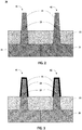
- FIG. 2 is a cross-sectional view illustrating the substrate structure of block S101.
- a substrate structure 20 includes a substrate (e.g., silicon) 21, a multitude of semiconductor fins (first fins) 31 protrude from the substrate structure.
- First fins 31 include a semiconductor layer 23 as the main body.
- semiconductor layer 23 may be silicon (Si) or silicon germanium (SiGe).
- first fins 31 may include a first set of fins 41 and a second set of fins 42.
- First set of fins 41 may be configured to form NMOS transistor devices, and second set of fins may be configured to form PMOS transistor devices.
- the number of fins can be any integer number. In the example shown in FIG. 2 , two fins are used, but it is understood that the number is arbitrary chosen for describing the example embodiment and should not be limiting.
- substrate structure 20 may further include a dielectric layer (e.g., silicon dioxide) 22 on substrate 21.
- a dielectric layer e.g., silicon dioxide
- first fins 31 protrude from dielectric layer 22.
- semiconductor layer 23 may extends through dielectric layer 23 into the substrate.
- substrate 21 is shown as a bulk silicon substrate in FIG. 2 , it is understood, however, that the invention is not limited thereto.
- substrate 21 may be an SOI substrate.
- the substrate structure may be formed by firstly forming a plurality of initial fins on the substrate by etching the substrate using a patterned mask.
- an insulating layer e.g., silicon dioxide
- the insulating layer is etched back to expose a portion of the initial fins.
- fin refers to a vertical structure protruding from the substrate structure, which includes the substrate or the substrate and the dielectric layer disposed thereon, however, the term “fin” may also refer broadly as the fin structure of a FinFET device.
- a liner oxide layer may be formed on the surface of the fins using an atomic layer deposition process to repair damage caused by etching.
- an ion implantation process may be performed into the fins to form a well region in the fins.
- a P-type well region may be formed in the fins to form NMOS transistor devices, and an N-type well region may be formed in the fins to form PMOS transistor devices.
- the liner oxide layer may be removed.
- an anti-punch through (APT) implant process and an annealing process may be performed on the fins.
- APT anti-punch through
- an epitaxial growth process is perform to form an epitaxial grown layer on the first fins, thereby forming second fins including the semiconductor layer and the epitaxial layer.
- FIG. 3 is a cross-sectional view illustrating the substrate structure of block S102.
- an epitaxial growth process is performed on first fins 31 to form an epitaxial layer 24, so that second fins are formed including semiconductor layer 23 and epitaxial layer 24. It is understood that the second fins are an intermediate structure.
- Epitaxial layer 24 may be of silicon, silicon germanium, or a III-V compound (e.g., GaAs), and the like. In some embodiments, epitaxial layer 24 has a thickness in the range between 1 nm and 2 nm.
- the epitaxial growth process may be an in-situ epitaxial growth process doped with phosphorus or arsenic.
- an N-type doped epitaxial layer may be formed on the first set of fins 41 and the second set of fins 42.
- a doping process may be performed after the formation of the epitaxial layer.
- the in-situ doped epitaxial growth process may be performed separately on the first set of fins 41 and on the second set of fins 42.
- an insulating layer (not shown) is formed on the second set of fins exposing the first set of fins, an in-situ epitaxial growth process doped with phosphorus or arsenic is performed on first set of fins 41. Thereafter, the insulating layer is removed.
- an in-situ epitaxial growth process doped with boron is performed on second set of fins 42.
- an N-type doped epitaxial layer is formed on first set of fins 41, and a P-type doped epitaxial layer is formed on second set of fins 42.
- a P-type doped epitaxial layer may be formed on first set of fins 41, and an N-type doped epitaxial layer may be formed on second set of fins 42.
- a first gate insulating layer is formed on the epitaxial layer, a first gate material layer is formed on the first gate insulating layer, and a hardmask layer is formed on the first gate material layer.
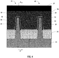
- FIG. 4 is a cross-sectional view illustrating the substrate structure of block S103.
- a first gate insulating layer 25 is formed on epitaxial layer 24
- a first gate material layer 26 is formed on first gate insulating layer 25, and a hardmask layer 27 is formed on first gate material layer 26.
- a first gate insulating layer may be formed on epitaxial layer 24 using an oxidation or deposition process.
- a gate material layer is formed on the first gate insulating layer using a deposition process.
- a planarization (e.g., CMP) process is performed on the first gate material layer to obtain a planar surface of the first gate material layer, a hard mask layer is then deposited on the first gate material layer.
- a portion of the hardmask layer, a portion of the first gate material layer, and a portion of the first gate insulating layer are removed by etching using a patterned mask (not shown) as a mask to form a first structure that exposes a portion of the second fins.
- the first structure includes a first gate insulation material on the epitaxial layer, a first gate electrode on the first gate insulation material, and the hard mask on the first gate electrode.
- FIG. 5 is a cross-sectional view of FIG. 4 taken along the line AA' according to block S104.
- hardmask layer 27, first gate material layer 26, first gate insulating layer 25 are etched using a patterned mask (e.g., a patterned photoresist) as an etching mask to form a first structure 61 and expose a portion of second fin 32 that is not covered by first structure 61.
- First structure 61 includes first gate insulating material 25 on epitaxial layer 24, first gate electrode 26 on first gate insulating material 25, and a hardmask 27 on first gate electrode 26. It is noted that first structure 61 is above dielectric layer 22, as is clearly shown in FIG. 6B .
- FIG. 5 illustrates a structure of first set of fins 41.
- the structure of the second set of fins may have a substantially same structure of the first set of fins following similar or substantially same processes of forming the first set of fins.
- the second set of fins may be formed similarly using substantially same processes of forming the first set of fins, and the processes will not be repeated for the sake of brevity.
- an etching process is performed on the exposed portion of the second fins to remove at least the epitaxial layer to form third fins.
- the third fins each include a portion covered by the first structure. For the sake of clarity, in the following description, only one fin is shown.
- FIG. 6A is a cross-sectional view illustrating a structure according to block S105.
- FIGS. 6B and 6C are cross-sectional views of the structure of FIG. 6A taken along the line BB' and CC', respectively.
- Third fin 33 includes a first portion 231 of semiconductor layer 23 covered by first structure 61.
- the etching process removes in addition to the at least one portion of epitaxial layer 24 also a portion of semiconductor layer 23, i.e., a portion of the main body.
- the etching process includes an over-etching step for etching a portion of the main body.
- the etched portion of semiconductor layer 23 may have a thickness in the range between 1 nm and 3 nm. As can be seen from FIGS.
- a portion of the top surface and lateral surfaces of the exposed portion of the semiconductor layer are removed by the etching process, so that the exposed top surface of the semiconductor layer is lower than the first portion 231 covered by the first structure, and the width of the etched lateral surfaces of the semiconductor layer is narrower than the width of the first portion of the main body.
- the thus formed semiconductor device has the channel moved down from the vicinity of the interface between the active region and the gate dielectric layer during operation, so that the generated hot carriers do not enter the gate electrode, thereby improving the semiconductor device reliability.
- sidewall spacers are formed on sidewalls of the first structure, the sidewall spacers extend to the upper surface of a second portion of the third fin, the second portion is disposed on opposite sides of the first portion, the first portion protrudes from the second portion, and the upper surface of the second portion is lower than the upper surface of the first portion.
- FIG. 7 is a cross-sectional view illustrating a structure of FIG. 6A after performing block S106.
- sidewall spacers 51 are formed on the sidewalls of the first structure. Sidewall spacers 51 extend to cover the surface of the second portion 232 of third fin 33.
- Second portion 232 is disposed on opposite sides of first portion 231. First portion 231 protrudes from second portion 232. The upper surface of second portion 232 is lower than the upper surface of first portion 231.
- an etching process is performed on the third fin to form a third portion in the second portion with respect to the outer surface of the first portion.
- the upper surface of the third portion is lower than the upper surface of the second portion.
- FIG. 8 is a cross-sectional view illustrating a structure of FIG. 7 after performing block S107.
- an etching process is performed on third fin 33 to form a third portion 233 in second portion 232 with respect to the outer surface of first portion 231.
- the upper surface of third portion 233 is lower than the upper surface of second portion 232.
- the etching process is a self-aligned etching process using first structure 61 and sidewall spacer 51 as an etching mask.
- a source region and a drain region are epitaxially formed on the third portion at an outer side of the sidewall spacers of the first structure, the upper surface of the source and drain regions is higher than the upper surface of the second portion.
- FIG. 9A is a cross-sectional view illustrating a structure of FIG. 8 after performing block S108.
- FIG. 9B is a cross-sectional view of the structure of FIG. 9A taken along the line DD'.
- a source region 52 and a drain region 53 are epitaxially formed on third portion 233 and adjacent sidewall spacers 51 outside first structure 61.
- the upper surface of source region 52 and drain region 53 is higher than the upper surface of second portion 232.
- semiconductor layer 23 includes silicon, source and drain regions 52, 53 include SiGe or SiP. That is, different materials can be epitaxially grown on third portion 233 to form source region 52 and drain region 53.
- the epitaxially formed source and drain regions have polygonal cross-sectional shapes (e.g., a hexagonal shape), as shown in FIG. 9B .
- the source and drain regions of the first set of fins may include SiP, and the source and drain regions of the second set of fins may include SiGe.
- the above-described embodiments of the present invention provide a method for manufacturing a semiconductor device.
- the channel is moved down from the interface of the active region and the gate insulating layer, so that the generated hot carriers during operations are further away from the interface so that they do not enter the gate electrode, thereby improving the reliability of the semiconductor device.
- method 100 may further include the following process steps:
- Interlayer dielectric layer 81 is formed on first structure 61.
- Interlayer dielectric layer 81 may include silicon dioxide.
- interlayer dielectric layer 81 is etched back to expose a surface of hardmask layer 27, as shown in FIG. 11 .
- a planarization (CMP) process may be performed on interlayer dielectric layer 81 to expose a surface of hardmask layer 27.
- hardmask layer 27, first gate electrode 26, and first gate insulating layer 25 are removed to form a trench 54, as shown in FIG. 12 .
- the gate structure may include a second gate insulating layer 56 on first portion 231, and a second gate electrode 57 on second gate insulating layer 56.
- the second gate electrode may include a metal (e.g., copper, aluminum, tungsten, or the like), or a metal compound (e.g., tantalum nitride).
- the second gate insulating layer may include an interface layer (e.g., a silicon oxide layer) on the first portion, and a high-k dielectric layer on the interface layer.
- the second gate electrode is formed on the high-k dielectric layer.
- embodiments of the present invention provide a method for manufacturing a semiconductor device. Based on processes described in blocks S101 through S108, a gate structure is formed. For an NMOS device, when the inversion layer is formed in the channel between the source and drain regions, an accumulation layer is generated on the inversion layer. Hot carriers may be generated at the side of the drain region and move much deeper below the gate insulating layer by the accumulation layer, thereby reducing the probability that hot carriers enter the gate insulating layer, so that the reliability of the semiconductor device is improved.
- a semiconductor device includes a substrate structure having a substrate 21, and a plurality of semiconductor fins 33 (i.e., third fin 33 described in above sections) each including a semiconductor layer 23.
- the semiconductor fin 33 includes a first portion 231, a second portion 232 disposed on opposite sides of first portion 231, and a third portion 233 disposed at the outer side of first portion 231 and adjacent second portion 232.
- First portion 231 protrudes from second portion 232, the upper surface of second portion 232 is lower than the upper surface of first portion 231, and the upper surface of third portion 233 is lower than the upper surface of second portion 232.
- the semiconductor device also includes a gate structure on an upper surface of first portion 231, sidewall spacers 51 on opposite sides of the gate structure, and a source region 52 and a drain region 53 on third portion 233 and at the outer side of sidewall spacers 51.
- the upper surface of the source and drain regions is higher than the upper surface of second portion 232.
- the sidewall spacers are disposed on the upper surface of second portion 232.
- the gate structure may include a gate insulating layer 56 on first portion 231 of semiconductor layer 23 and a gate electrode 57 on the gate insulating layer.
- the gate electrode may include polysilicon, metal (e.g., copper, aluminum, tungsten), and/or electrically conductive functional layer.
- the conductive functional layer may include a metal and a metal compound chosen from a metal nitride (e.g., tantalum nitride).
- the gate insulating layer may include an interface layer (e.g., silicon oxide layer) on a portion of the first portion and a high-k dielectric layer on the interface layer.
- the gate electrode is disposed on the high-k dielectric layer.
- first portion 231 may include an epitaxial layer 24, which is adjacent to the gate structure.
- first portion 231 protrudes from the lateral surfaces and the upper surface of the second portion.
- the plurality of fins may include a first set of fins configured to form NMOS transistor devices and a second set of fins configured to form PMOS transistor devices.
- FIG. 13 only illustrates one set of fins, however, those of skill in the art will appreciate that a second set of fins have the same or substantially the same structure.
- the portion (e.g., epitaxial layer 24) of the first portion of the first set of fins protruding from the second portion includes an N-type conductive material; and the portion of the first portion of the second set of fins protruding from the second portion includes an N-type conductive material.
- the portion of the first portion of the first set of fins protruding from the second portion includes a P-type conductive material; and the portion of the first portion of the second set of fins protruding from the second portion includes an N-type conductive material.
- the portion of the first portion protruding from the second portion has a thickness in the range between 1 nm and 5 nm. In some embodiments, epitaxial layer 24 has a thickness in the range between 1 nm and 2 nm.
- the semiconductor layer 23 of the fins includes silicon or SiGe, and the source and drain regions may include SiGe or SiP.
- the semiconductor layer 23 of the fins includes silicon or SiGe
- the source and drain regions of the first set of fins include SiP
- the source and drain regions of the second set of fins include SiGe.
- the substrate structure may further include a dielectric layer 22 on substrate 21.
- the fins 33 protrude from the dielectric layer, and the gate structure is on the dielectric layer.
- the semiconductor device may also include an interlayer dielectric layer 81 on the substrate structure.
- Interlayer dielectric layer 81 surrounds the sidewall spacers 51 and the gate structure.
- hot carriers generated during the operation of the semiconductor device can be moved further away from the gate insulating layer to prevent them from entering the gate insulating layer, thereby improving the reliability of the semiconductor device.
Landscapes
- Insulated Gate Type Field-Effect Transistor (AREA)
- Metal-Oxide And Bipolar Metal-Oxide Semiconductor Integrated Circuits (AREA)
Abstract
Description
- This application claims priority to Chinese patent application No.
201610091575.8, filed on February 19, 2016 - The present invention relates to the field of semiconductor device fabrication. In particular, the present invention relates to a fin field effect transistor device having improved hot carrier reliability and method for manufacturing the same.
- Fin field-effect transistor (FinFET) devices have the ability to control short-channel effects, high drive current, low power consumption, and show promise to continue to follow Moore's Law. However, the hot-channel injection effect will adversely affect the reliability of FinFET devices. Currently, there is no effective techniques to suppress hot-channel injection (HCI) effects in FinFET devices.
- Thus, there is a need for an improved FinFET structure and method for manufacturing the same to suppress HCI effects.
- The present invention provides a semiconductor device and method for manufacturing the same to suppress hot carrier effects.
- According to a first aspect of the present invention, a semiconductor device includes: a substrate structure including a substrate, a plurality of semiconductor fins protruding from the substrate structure, each of the semiconductor fins comprising a first portion, a second portion on opposite sides of the first portion, and a third portion at an outer side of the first portion and adjacent to the second portion. The first portion protrudes from the second portion and has an upper surface, the second portion has an upper surface that is lower than the upper surface of the first portion, and the third portion has an upper surface that is lower than the upper surface of the second portion. The semiconductor device further includes a gate structure on the upper surface of the first portion, sidewall spacers on opposite sides of the gate structure and covering the upper surface of the second portion, and a source region and a drain region on the third portion and at an outer side of the sidewall spacers, the source and drain regions each having an upper surface higher than the upper surface of the second portion.
- Preferably, the first portion comprises an epitaxial layer adjacent to the gate structure, and protrudes from the upper surface of the second portion.
- Preferably, the plurality of fins comprises a first set of fins configured to form a plurality of NMOS transistor devices and a second set of fins configured to form a plurality of PMOS transistor devices. A portion of the first portion of the first set of fins protruding from the second portion may include an N-type conductive material, and a portion of the first portion of the second set of fins protruding from the second portion includes an N-type conductive material.
- Preferably, a portion of the first portion of the first set of fins protruding from the second portion includes a P-type conductive material, and a portion of the first portion of the second set of fins protruding from the second portion includes an N-type conductive material.
- Preferably, the semiconductor fins comprise silicon (Si) or silicon germanium (SiGe), the source and drain regions of the first set of fins include silicon phosphorus (SiP), and the source and drain regions of the second set of fins include SiGe.
- Preferably, a portion of the first portion protruding from the second portion has a thickness in a range between 1 nm and 5 nm.
- Preferably, the semiconductor fins comprise silicon or SiGe, and the source and drain regions comprise SiGe or SiP.
- Preferably, the substrate structure further comprises a dielectric layer on the substrate, and the fins protrude from the dielectric layer.
- Preferably, the semiconductor device further includes an interlayer dielectric layer on the substrate structure, and the interlayer dielectric layer surrounds the sidewall spacers and the gate structure.
- Preferably, the gate structure includes a gate insulating layer on the first portion and a gate electrode on the gate insulating layer. The gate electrode may include polysilicon, metal or a conductive functional layer.
- A second aspect of the present invention provides a method for manufacturing a semiconductor device. The method includes: providing a substrate structure including a substrate, forming a plurality of first fins having a semiconductor layer on the substrate, performing an epitaxial growth process on the semiconductor layer of the plurality of first fins to form a plurality of second fins having an epitaxial layer, forming a first gate insulating layer on the epitaxial layer, a gate material layer on the first gate insulating layer, and a hardmask layer on the gate material layer, performing a first etching process using a pattern mask to remove a portion of the hardmask layer, a portion of the gate material layer, and a portion of the first gate insulating layer to form a first structure and exposing a portion of the second fins not covered by the first structure, and performing a second etching process to remove at least the epitaxial layer in the exposed portion of the second fins to form a plurality of third fins, the third fins comprising a first portion of the semiconductor layer covered by the first structure. The method further includes: forming sidewall spacers on the first structure, the sidewall spacers being disposed on an upper surface of a second portion of the third fins, the second portion being on opposite sides of the first portion and having an upper surface lower than an upper surface of the first portion. The method also includes: performing a third etching process to form a third portion at an outer side of the first portion and adjacent to the second portion, the third portion having an upper surface lower than the upper surface of the second portion, and forming a source region and a drain region outside of the sidewall spacers and on the third portion. Preferably, the source and drain regions each have an upper surface higher than the upper surface of the second portion.
- Preferably, the method also includes: forming an interlayer dielectric layer on the first structure, etching back the interlayer dielectric layer to expose the hardmask layer, removing the hardmask layer, the gate electrode, and the first gate insulating layer to form a trench, and forming a gate structure in the trench.
- Preferably, the gate structure includes a second gate insulating layer on the first portion, and a second gate electrode on the second gate insulating layer.
- Preferably, performing the second etching process to remove at least the epitaxial layer in the exposed portion of the second fins further includes removing a portion of the semiconductor layer below the epitaxial layer.
- Preferably, the removed portion of the semiconductor layer has a thickness in a range between 1 nm and 3 nm.
- Preferably, the fins includes a first set of fins configured to form a plurality of NMOS transistor devices and a second set of fins configured to form a plurality of PMOS transistor devices.
- Preferably, the epitaxial growth process is an in-situ epitaxial growth process doped with phosphorus or arsenic.
- Preferably, the epitaxial layer has a thickness in the range between 1 nm and 2 nm.
- Preferably, the semiconductor layer includes silicon or SiGe, and the source and drain regions include SiGe or SiP.
- Preferably, the semiconductor layer includes silicon or SiGe, the source and drain regions of the first set of fins include SiP, and the source and drain regions of the second set of fins include SiGe.
- Preferably, the substrate structure further comprises a dielectric layer on the substrate, and the fins protrude from the dielectric layer.
- Preferably, the semiconductor device further includes an interlayer dielectric layer on the substrate structure, and the interlayer dielectric layer surrounds the sidewall spacers and the gate structure.
- Preferably, the gate structure includes a gate insulating layer on the first portion and a gate electrode on the gate insulating layer. The gate electrode may include: polysilicon, metal or a conductive functional layer.
- A semiconductor device according to the first aspect of the present invention is obtainable by a method according to the second aspect of the present invention.
- The following description, together with the accompanying drawings, will provide a better understanding of the nature and advantages of the claimed invention.
- The accompanying drawings, referred to herein and constituting a part hereof, illustrate embodiments of the invention. The drawings together with the description serve to explain the principles of the invention.
-
FIG. 1 is a flowchart diagram illustrating a manufacturing method according to an embodiment of the present invention. -
FIG. 2 is a cross-sectional view of an intermediate stage of a manufacturing method according to some embodiments of the present invention. -
FIG. 3 is a cross-sectional view of an intermediate stage of a manufacturing method according to some embodiments of the present invention. -
FIG. 4 is a cross-sectional view of an intermediate stage of a manufacturing method according to some embodiments of the present invention. -
FIG. 5 is a cross-sectional view of an intermediate stage of a manufacturing method according to some embodiments of the present invention. -
FIG. 6A is a cross-sectional view of an intermediate stage of a manufacturing method according to some embodiments of the present invention. -
FIG. 6B is a cross-sectional view ofFIG. 6A taken along the line B-B'. -
FIG. 6C is a cross-sectional view of ofFIG. 6A taken along the line C-C'. -
FIG. 7 is a cross-sectional view of an intermediate stage of a manufacturing method according to some embodiments of the present invention. -
FIG. 8 is a cross-sectional view of an intermediate stage of a manufacturing method according to some embodiments of the present invention. -
FIG. 9A is a cross-sectional view of an intermediate stage of a manufacturing method according to some embodiments of the present invention. -
FIG. 9B is a cross-sectional view ofFIG. 9A taken along the line D-D'. -
FIG. 10 is a cross-sectional view of an intermediate stage of a manufacturing method according to some embodiments of the present invention. -
FIG. 11 is a cross-sectional view of an intermediate stage of a manufacturing method according to some embodiments of the present invention. -
FIG. 12 is a cross-sectional view of an intermediate stage of a manufacturing method according to some embodiments of the present invention. -
FIG. 13 is a cross-sectional view of an intermediate stage of a manufacturing method according to some embodiments of the present invention. - In the following description, numerous specific details are provided for a thorough understanding of the present invention. However, it should be appreciated by those of skill in the art that the present invention may be realized without one or more of these details. In other examples, features and techniques known in the art will not be described for purposes of brevity.
- It should be understood that the drawings are not drawn to scale, and similar reference numbers are used for representing similar elements. Embodiments of the invention are described herein with reference to perspective cross-section illustrations that are schematic illustrations of idealized embodiments (and intermediate structures) of the invention. The thickness of layers and regions in the drawings may be exaggerated relative to each other for clarity. Additionally, variations from the shapes of the illustrations as a result, for example, of manufacturing techniques and/or tolerances, are to be expected. Thus, embodiments of the invention should not be construed as limited to the particular shapes of regions illustrated herein but are to include deviations in shapes that result, for example, from manufacturing.
- It will be understood that, when an element or layer is referred to as "on," "disposed on," "adjacent to," "connected to," or "coupled to" another element or layer, it can be disposed directly on the other element or layer, adjacent to, connected or coupled to the other element or layer, or intervening elements or layers may also be present. In contrast, when an element is referred to as being "directly on," directly disposed on," "directly connected to," or "directly coupled to" another element or layer, there are no intervening elements or layers present between them. It will be understood that, although the terms "first," "second," "third," etc. may be used herein to describe various elements, components, regions, layers and/or sections, these elements, components, regions, layers and/or sections should not be limited by these terms. These terms are only used to distinguish one element, component, region, layer or section from another region, layer or section. Thus, a first element, component, region, layer or section discussed below could be termed a second element, component, region, layer or section without departing from the teachings of the present invention.
- The use of the terms first, second, third, etc. do not denote any order, but rather the terms first, second, third, etc. are used to distinguish one element from another. Furthermore, the use of the terms a, an, etc. does not denote a limitation of quantity, but rather denote the presence of at least one of the referenced items.
- The term "substrate" may include any structure having an exposed surface with which to form an integrated circuit. The term "substrate" is understood to include semiconductor wafers and is also used to refer to semiconductor structures during processing and may include other layers that have been fabricated thereupon. A "substrate" may include doped and undoped semiconductor wafers, epitaxial semiconductor layers, as well as other semiconductor structures.
- In accordance with some embodiments of the present invention,
FIG. 1 is a flowchart illustrating amethod 100 for manufacturing a semiconductor device.FIGS. 2-5 ,6A ,6B, 6C ,7, 8 ,9A, 9B , and10-13 are cross-sectional views of intermediate stages of the manufacturing method according to some embodiments of the present invention. In the disclosure, each drawing or block in the flowchart represents a process associated with embodiments of the method described. Those of skill in the art will recognize that additional blocks and drawings that described the embodiments may be added. - Referring to
FIG. 1 , in block S101, a substrate structure is provided. The substrate structure includes a substrate. A plurality of first fins protrude from the substrate structure. The fin fins include a semiconductor layer serving as a main body. -
FIG. 2 is a cross-sectional view illustrating the substrate structure of block S101. As shown inFIG. 2 , asubstrate structure 20 includes a substrate (e.g., silicon) 21, a multitude of semiconductor fins (first fins) 31 protrude from the substrate structure.First fins 31 include asemiconductor layer 23 as the main body. For example,semiconductor layer 23 may be silicon (Si) or silicon germanium (SiGe). - In some embodiments, as shown in
FIG. 2 ,first fins 31 may include a first set offins 41 and a second set offins 42. First set offins 41 may be configured to form NMOS transistor devices, and second set of fins may be configured to form PMOS transistor devices. It is understood that the number of fins can be any integer number. In the example shown inFIG. 2 , two fins are used, but it is understood that the number is arbitrary chosen for describing the example embodiment and should not be limiting. - In some embodiments, as shown in
FIG. 2 ,substrate structure 20 may further include a dielectric layer (e.g., silicon dioxide) 22 onsubstrate 21. In this case,first fins 31 protrude fromdielectric layer 22. In other words,semiconductor layer 23 may extends throughdielectric layer 23 into the substrate. - Although
substrate 21 is shown as a bulk silicon substrate inFIG. 2 , it is understood, however, that the invention is not limited thereto. For example,substrate 21 may be an SOI substrate. - In some embodiments, the substrate structure may be formed by firstly forming a plurality of initial fins on the substrate by etching the substrate using a patterned mask.
- In the case that the initial substrate is a semiconductor substrate, after the initial fins have been formed, an insulating layer (e.g., silicon dioxide) may be formed on the initial fins. Thereafter, the insulating layer is etched back to expose a portion of the initial fins.
- It is to be understood that, as used herein, the term "fin" refers to a vertical structure protruding from the substrate structure, which includes the substrate or the substrate and the dielectric layer disposed thereon, however, the term "fin" may also refer broadly as the fin structure of a FinFET device.
- In some embodiments, after the formation of the initial fins, a liner oxide layer may be formed on the surface of the fins using an atomic layer deposition process to repair damage caused by etching. In some embodiments, an ion implantation process may be performed into the fins to form a well region in the fins. For example, a P-type well region may be formed in the fins to form NMOS transistor devices, and an N-type well region may be formed in the fins to form PMOS transistor devices. Then, optionally, the liner oxide layer may be removed. In some embodiments, an anti-punch through (APT) implant process and an annealing process may be performed on the fins.
- Referring back to
FIG. 1 , in block S102, an epitaxial growth process is perform to form an epitaxial grown layer on the first fins, thereby forming second fins including the semiconductor layer and the epitaxial layer. -
FIG. 3 is a cross-sectional view illustrating the substrate structure of block S102. For example, an epitaxial growth process is performed onfirst fins 31 to form anepitaxial layer 24, so that second fins are formed includingsemiconductor layer 23 andepitaxial layer 24. It is understood that the second fins are an intermediate structure.Epitaxial layer 24 may be of silicon, silicon germanium, or a III-V compound (e.g., GaAs), and the like. In some embodiments,epitaxial layer 24 has a thickness in the range between 1 nm and 2 nm. - The epitaxial growth process may be an in-situ epitaxial growth process doped with phosphorus or arsenic. For example, an N-type doped epitaxial layer may be formed on the first set of
fins 41 and the second set offins 42. However, the present invention is not limited thereto, for example, a doping process may be performed after the formation of the epitaxial layer. - In other embodiments, the in-situ doped epitaxial growth process may be performed separately on the first set of
fins 41 and on the second set offins 42. For example, an insulating layer (not shown) is formed on the second set of fins exposing the first set of fins, an in-situ epitaxial growth process doped with phosphorus or arsenic is performed on first set offins 41. Thereafter, the insulating layer is removed. Similarly, an in-situ epitaxial growth process doped with boron is performed on second set offins 42. Thus, an N-type doped epitaxial layer is formed on first set offins 41, and a P-type doped epitaxial layer is formed on second set offins 42. - In still other embodiments, a P-type doped epitaxial layer may be formed on first set of
fins 41, and an N-type doped epitaxial layer may be formed on second set offins 42. - Referring back to
FIG. 1 , in block S103, a first gate insulating layer is formed on the epitaxial layer, a first gate material layer is formed on the first gate insulating layer, and a hardmask layer is formed on the first gate material layer. -
FIG. 4 is a cross-sectional view illustrating the substrate structure of block S103. For example, a firstgate insulating layer 25 is formed onepitaxial layer 24, a firstgate material layer 26 is formed on firstgate insulating layer 25, and ahardmask layer 27 is formed on firstgate material layer 26. - In an exemplary embodiment, a first gate insulating layer may be formed on
epitaxial layer 24 using an oxidation or deposition process. Next, a gate material layer is formed on the first gate insulating layer using a deposition process. Preferably, a planarization (e.g., CMP) process is performed on the first gate material layer to obtain a planar surface of the first gate material layer, a hard mask layer is then deposited on the first gate material layer. - Referring back to
FIG. 1 , in block S104, a portion of the hardmask layer, a portion of the first gate material layer, and a portion of the first gate insulating layer are removed by etching using a patterned mask (not shown) as a mask to form a first structure that exposes a portion of the second fins. The first structure includes a first gate insulation material on the epitaxial layer, a first gate electrode on the first gate insulation material, and the hard mask on the first gate electrode. -
FIG. 5 is a cross-sectional view ofFIG. 4 taken along the line AA' according to block S104. As shown inFIG. 5 ,hardmask layer 27, firstgate material layer 26, firstgate insulating layer 25 are etched using a patterned mask (e.g., a patterned photoresist) as an etching mask to form afirst structure 61 and expose a portion ofsecond fin 32 that is not covered byfirst structure 61.First structure 61 includes firstgate insulating material 25 onepitaxial layer 24,first gate electrode 26 on firstgate insulating material 25, and ahardmask 27 onfirst gate electrode 26. It is noted thatfirst structure 61 is abovedielectric layer 22, as is clearly shown inFIG. 6B . - It is noted that
FIG. 5 illustrates a structure of first set offins 41. Those of skill in the art will appreciate that the structure of the second set of fins may have a substantially same structure of the first set of fins following similar or substantially same processes of forming the first set of fins. In the subsequent processes, unless explicitly stated, the second set of fins may be formed similarly using substantially same processes of forming the first set of fins, and the processes will not be repeated for the sake of brevity. - Referring back to
FIG. 1 , in block S105, an etching process is performed on the exposed portion of the second fins to remove at least the epitaxial layer to form third fins. The third fins each include a portion covered by the first structure. For the sake of clarity, in the following description, only one fin is shown. -
FIG. 6A is a cross-sectional view illustrating a structure according to block S105.FIGS. 6B and 6C are cross-sectional views of the structure ofFIG. 6A taken along the line BB' and CC', respectively. - As shown in
FIG. 6A , an etching process is performed on the exposed portion ofsecond fin 32 to remove at least one portion ofepitaxial layer 24 to form athird fin 33.Third fin 33 includes afirst portion 231 ofsemiconductor layer 23 covered byfirst structure 61. - In some embodiments, the etching process removes in addition to the at least one portion of
epitaxial layer 24 also a portion ofsemiconductor layer 23, i.e., a portion of the main body. For example, the etching process includes an over-etching step for etching a portion of the main body. In an embodiment, the etched portion ofsemiconductor layer 23 may have a thickness in the range between 1 nm and 3 nm. As can be seen fromFIGS. 6A and6B , a portion of the top surface and lateral surfaces of the exposed portion of the semiconductor layer are removed by the etching process, so that the exposed top surface of the semiconductor layer is lower than thefirst portion 231 covered by the first structure, and the width of the etched lateral surfaces of the semiconductor layer is narrower than the width of the first portion of the main body. - Through the removal of the epitaxial layer and a portion of the semiconductor layer below the epitaxial layer, the thus formed semiconductor device has the channel moved down from the vicinity of the interface between the active region and the gate dielectric layer during operation, so that the generated hot carriers do not enter the gate electrode, thereby improving the semiconductor device reliability.
- Referring back to
FIG. 1 , in block S106, sidewall spacers are formed on sidewalls of the first structure, the sidewall spacers extend to the upper surface of a second portion of the third fin, the second portion is disposed on opposite sides of the first portion, the first portion protrudes from the second portion, and the upper surface of the second portion is lower than the upper surface of the first portion. -
FIG. 7 is a cross-sectional view illustrating a structure ofFIG. 6A after performing block S106. As shown inFIG. 7 ,sidewall spacers 51 are formed on the sidewalls of the first structure.Sidewall spacers 51 extend to cover the surface of thesecond portion 232 ofthird fin 33.Second portion 232 is disposed on opposite sides offirst portion 231.First portion 231 protrudes fromsecond portion 232. The upper surface ofsecond portion 232 is lower than the upper surface offirst portion 231. - Referring back to
FIG. 1 , in block S107, an etching process is performed on the third fin to form a third portion in the second portion with respect to the outer surface of the first portion. The upper surface of the third portion is lower than the upper surface of the second portion. -
FIG. 8 is a cross-sectional view illustrating a structure ofFIG. 7 after performing block S107. As shown inFIG. 8 , an etching process is performed onthird fin 33 to form athird portion 233 insecond portion 232 with respect to the outer surface offirst portion 231. The upper surface ofthird portion 233 is lower than the upper surface ofsecond portion 232. Note that the etching process is a self-aligned etching process usingfirst structure 61 andsidewall spacer 51 as an etching mask. - Referring back to
FIG. 1 , in block S108, a source region and a drain region are epitaxially formed on the third portion at an outer side of the sidewall spacers of the first structure, the upper surface of the source and drain regions is higher than the upper surface of the second portion. -
FIG. 9A is a cross-sectional view illustrating a structure ofFIG. 8 after performing block S108.FIG. 9B is a cross-sectional view of the structure ofFIG. 9A taken along the line DD'. As shown inFIGS. 9A and 9B , asource region 52 and adrain region 53 are epitaxially formed onthird portion 233 andadjacent sidewall spacers 51 outsidefirst structure 61. The upper surface ofsource region 52 and drainregion 53 is higher than the upper surface ofsecond portion 232. - In some embodiments,
semiconductor layer 23 includes silicon, source and drainregions third portion 233 to formsource region 52 and drainregion 53. The epitaxially formed source and drain regions have polygonal cross-sectional shapes (e.g., a hexagonal shape), as shown inFIG. 9B . - In some embodiments, the source and drain regions of the first set of fins may include SiP, and the source and drain regions of the second set of fins may include SiGe.
- Thus, the above-described embodiments of the present invention provide a method for manufacturing a semiconductor device. By shifting the channel region with respect to the sidewall spacers (with respect to the lower portion of the sidewall spacers or with respect to the channel location), the channel is moved down from the interface of the active region and the gate insulating layer, so that the generated hot carriers during operations are further away from the interface so that they do not enter the gate electrode, thereby improving the reliability of the semiconductor device.
- According to some embodiments of the present invention,
method 100 may further include the following process steps: - Referring to
FIG. 10 , aninterlayer dielectric layer 81 is formed onfirst structure 61.Interlayer dielectric layer 81 may include silicon dioxide. - Next,
interlayer dielectric layer 81 is etched back to expose a surface ofhardmask layer 27, as shown inFIG. 11 . For example, a planarization (CMP) process may be performed oninterlayer dielectric layer 81 to expose a surface ofhardmask layer 27. - Next,
hardmask layer 27,first gate electrode 26, and firstgate insulating layer 25 are removed to form atrench 54, as shown inFIG. 12 . - Next, a gate structure is formed in
trench 54, as shown inFIG. 13 . In some embodiments, the gate structure may include a secondgate insulating layer 56 onfirst portion 231, and asecond gate electrode 57 on secondgate insulating layer 56. In an exemplary embodiment, the second gate electrode may include a metal (e.g., copper, aluminum, tungsten, or the like), or a metal compound (e.g., tantalum nitride). - In some embodiments, the second gate insulating layer may include an interface layer (e.g., a silicon oxide layer) on the first portion, and a high-k dielectric layer on the interface layer. The second gate electrode is formed on the high-k dielectric layer.
- Thus, embodiments of the present invention provide a method for manufacturing a semiconductor device. Based on processes described in blocks S101 through S108, a gate structure is formed. For an NMOS device, when the inversion layer is formed in the channel between the source and drain regions, an accumulation layer is generated on the inversion layer. Hot carriers may be generated at the side of the drain region and move much deeper below the gate insulating layer by the accumulation layer, thereby reducing the probability that hot carriers enter the gate insulating layer, so that the reliability of the semiconductor device is improved.
- Embodiments of the present invention also provide a semiconductor device. Referring to
FIG. 13 , a semiconductor device includes a substrate structure having asubstrate 21, and a plurality of semiconductor fins 33 (i.e.,third fin 33 described in above sections) each including asemiconductor layer 23. Thesemiconductor fin 33 includes afirst portion 231, asecond portion 232 disposed on opposite sides offirst portion 231, and athird portion 233 disposed at the outer side offirst portion 231 and adjacentsecond portion 232.First portion 231 protrudes fromsecond portion 232, the upper surface ofsecond portion 232 is lower than the upper surface offirst portion 231, and the upper surface ofthird portion 233 is lower than the upper surface ofsecond portion 232. - The semiconductor device also includes a gate structure on an upper surface of
first portion 231,sidewall spacers 51 on opposite sides of the gate structure, and asource region 52 and adrain region 53 onthird portion 233 and at the outer side ofsidewall spacers 51. The upper surface of the source and drain regions is higher than the upper surface ofsecond portion 232. The sidewall spacers are disposed on the upper surface ofsecond portion 232. - Referring still to
FIG. 13 , the gate structure may include agate insulating layer 56 onfirst portion 231 ofsemiconductor layer 23 and agate electrode 57 on the gate insulating layer. The gate electrode may include polysilicon, metal (e.g., copper, aluminum, tungsten), and/or electrically conductive functional layer. The conductive functional layer may include a metal and a metal compound chosen from a metal nitride (e.g., tantalum nitride). - In some embodiments, the gate insulating layer may include an interface layer (e.g., silicon oxide layer) on a portion of the first portion and a high-k dielectric layer on the interface layer. The gate electrode is disposed on the high-k dielectric layer.
- In some embodiments,
first portion 231 may include anepitaxial layer 24, which is adjacent to the gate structure. - In some embodiments,
first portion 231 protrudes from the lateral surfaces and the upper surface of the second portion. - In some embodiments, the plurality of fins may include a first set of fins configured to form NMOS transistor devices and a second set of fins configured to form PMOS transistor devices.
FIG. 13 only illustrates one set of fins, however, those of skill in the art will appreciate that a second set of fins have the same or substantially the same structure. - In some embodiments, the portion (e.g., epitaxial layer 24) of the first portion of the first set of fins protruding from the second portion includes an N-type conductive material; and the portion of the first portion of the second set of fins protruding from the second portion includes an N-type conductive material.
- In some embodiments, the portion of the first portion of the first set of fins protruding from the second portion includes a P-type conductive material; and the portion of the first portion of the second set of fins protruding from the second portion includes an N-type conductive material.
- In some embodiments, the portion of the first portion protruding from the second portion has a thickness in the range between 1 nm and 5 nm. In some embodiments,
epitaxial layer 24 has a thickness in the range between 1 nm and 2 nm. - In some embodiments, the
semiconductor layer 23 of the fins includes silicon or SiGe, and the source and drain regions may include SiGe or SiP. - In some embodiments, the
semiconductor layer 23 of the fins includes silicon or SiGe, the source and drain regions of the first set of fins include SiP, and the source and drain regions of the second set of fins include SiGe. - Referring still to
FIG. 13 , the substrate structure may further include adielectric layer 22 onsubstrate 21. Thefins 33 protrude from the dielectric layer, and the gate structure is on the dielectric layer. - Referring still to
FIG. 13 , the semiconductor device may also include aninterlayer dielectric layer 81 on the substrate structure.Interlayer dielectric layer 81 surrounds thesidewall spacers 51 and the gate structure. - In accordance to embodiments of the present invention, hot carriers generated during the operation of the semiconductor device can be moved further away from the gate insulating layer to prevent them from entering the gate insulating layer, thereby improving the reliability of the semiconductor device.
- Preferred embodiments of the present invention have been described in detail hereinabove.
- Furthermore, some of the features of the preferred embodiments of the present invention could be used to advantage without the corresponding use of other features. As such, the foregoing description should be considered as merely illustrative of the principles of the invention, and not in limitation thereof.
Claims (15)
- A semiconductor device comprising:a substrate structure including a substrate;a plurality of semiconductor fins protruding from the substrate structure, each of the semiconductor fins comprising a first portion, a second portion on opposite sides of the first portion, and a third portion at an outer side of the first portion and adjacent to the second portion, the first portion protruding from the second portion and having an upper surface, the second portion having an upper surface lower than the upper surface of the first portion, and the third portion having an upper surface lower than the upper surface of the second portion;a gate structure on the upper surface of the first portion;sidewall spacers on opposite sides of the gate structure and covering the upper surface of the second portion; anda source region and a drain region on the third portion and at an outer side of the sidewall spacers, the source and drain regions each having an upper surface higher than the upper surface of the second portion.
- The semiconductor device of claim 1, wherein:the first portion comprises an epitaxial layer adjacent to the gate structure; and/orthe first portion protrudes from the upper surface of the second portion.
- The semiconductor device of claim 1 or 2, wherein the plurality of fins comprises a first set of fins configured to form a plurality of NMOS transistor devices and a second set of fins configured to form a plurality of PMOS transistor devices; and
wherein preferably: the semiconductor fins comprise silicon or silicon germanium (SiGe); the source and drain regions of the first set of fins comprise silicon phosphorus (SiP); and the source and drain regions of the second set of fins comprise SiGe. - The semiconductor device of claim 3, wherein:a portion of the first portion of the first set of fins protruding from the second portion comprises an N-type conductive material, and a portion of the first portion of the second set of fins protruding from the second portion comprises an N-type conductive material; or, alternatively,a portion of the first portion of the first set of fins protruding from the second portion comprises a P-type conductive material, and a portion of the first portion of the second set of fins protruding from the second portion comprises an N-type conductive material.
- The semiconductor device of any one of the claims 1-4, wherein:a portion of the first portion protruding from the second portion has a thickness in a range between 1 nm and 5 nm; and/orthe semiconductor fins comprise silicon or SiGe, and the source and drain regions comprise SiGe or SiP.
- The semiconductor device of any one of the claims 1-5, wherein the substrate structure further comprises a dielectric layer on the substrate, and the fins protrude from the dielectric layer.
- The semiconductor device of any one of the claims 1-6, further comprising an interlayer dielectric layer on the substrate structure, the interlayer dielectric layer surrounding the sidewall spacers and the gate structure.
- The semiconductor device of any one of the claims 1-7, wherein the gate structure comprises a gate insulating layer on the first portion and a gate electrode on the gate insulating layer; and
wherein preferably: the gate electrode comprises polysilicon, metal or a conductive functional layer. - A method for manufacturing a semiconductor device, the method comprising:providing a substrate structure including a substrate;forming a plurality of first fins having a semiconductor layer on the substrate;performing an epitaxial growth process on the semiconductor layer of the plurality of first fins to form a plurality of second fins having an epitaxial layer;forming a first gate insulating layer on the epitaxial layer, a gate material layer on the first gate insulating layer, and a hardmask layer on the gate material layer;performing a first etching process using a patterned mask to remove a portion of the hardmask layer, a portion of the gate material layer, and a portion of the first gate insulating layer to form a first structure and exposing a portion of the second fins not covered by the first structure;performing a second etching process to remove at least one portion of the epitaxial layer in the exposed portion of the second fins to form a plurality of third fins, the third fins comprising a first portion of the semiconductor layer covered by the first structure;forming sidewall spacers on the first structure, the sidewall spacers being disposed on an upper surface of a second portion of the third fins, the second portion being on opposite sides of the first portion and having an upper surface lower than an upper surface of the first portion;performing a third etching process to form a third portion at an outer side of the first portion and adjacent to the second portion, the third portion having an upper surface lower than the upper surface of the second portion; andforming a source region and a drain region outside of the sidewall spacers and on the third portion, the source and drain regions each having an upper surface higher than the upper surface of the second portion.
- The method of claim 9, further comprising:forming an interlayer dielectric layer on the first structure;etching back the interlayer dielectric layer to expose the hardmask layer;removing a portion of the hardmask layer, a portion of the gate electrode, and a portion of the first gate insulating layer to form a trench; andforming a gate structure in the trench.
- The method of claim 10, wherein forming the gate structure comprises:forming a second gate insulating layer on the first portion, andforming a second gate electrode on the second gate insulating layer.
- The method of any one of the claims 9-11, wherein performing the second etching process to remove the at least one portion of the epitaxial layer in the exposed portion of the second fins further comprises removing a portion of the semiconductor layer below the epitaxial layer.
- The method of claim 12, wherein the removed portion of the semiconductor layer has a thickness in a range between 1 nm and 3 nm.
- The method of any one of the claims 9-13, wherein the plurality of fins comprises a first set of fins configured to form a plurality of NMOS transistor devices and a second set of fins configured to form a plurality of PMOS transistor devices.
- The method of any one of the claims 9-14, wherein the epitaxial growth process is an in-situ epitaxial growth process doped with phosphorus or arsenic.
Applications Claiming Priority (1)
| Application Number | Priority Date | Filing Date | Title |
|---|---|---|---|
| CN201610091575.8A CN107104143B (en) | 2016-02-19 | 2016-02-19 | Semiconductor device and method for manufacturing the same |
Publications (2)
| Publication Number | Publication Date |
|---|---|
| EP3208836A1 true EP3208836A1 (en) | 2017-08-23 |
| EP3208836B1 EP3208836B1 (en) | 2019-12-25 |
Family
ID=58017987
Family Applications (1)
| Application Number | Title | Priority Date | Filing Date |
|---|---|---|---|
| EP17155783.8A Active EP3208836B1 (en) | 2016-02-19 | 2017-02-13 | A method to improve hci performance for finfet |
Country Status (3)
| Country | Link |
|---|---|
| US (1) | US9875944B2 (en) |
| EP (1) | EP3208836B1 (en) |
| CN (1) | CN107104143B (en) |
Families Citing this family (3)
| Publication number | Priority date | Publication date | Assignee | Title |
|---|---|---|---|---|
| CN109686779B (en) * | 2017-10-19 | 2022-05-13 | 中芯国际集成电路制造(上海)有限公司 | Semiconductor structure and forming method thereof |
| US10727323B2 (en) * | 2018-01-08 | 2020-07-28 | International Business Machines Corporation | Three-dimensional (3D) tunneling field-effect transistor (FET) |
| US10964598B2 (en) | 2019-07-18 | 2021-03-30 | Globalfoundries U.S. Inc. | Methods of forming source/drain regions of a FinFET device and the resulting structures |
Citations (4)
| Publication number | Priority date | Publication date | Assignee | Title |
|---|---|---|---|---|
| US20140291737A1 (en) * | 2013-03-29 | 2014-10-02 | Walid M. Hafez | Transistor architecture having extended recessed spacer and source/drain regions and method of making same |
| US20150001593A1 (en) * | 2013-06-28 | 2015-01-01 | Taiwan Semiconductor Manufacturing Co., Ltd. | Method for Forming Multi-Gate Device with Dual Channel |
| US20150206956A1 (en) * | 2014-01-21 | 2015-07-23 | Samsung Electronics Co., Ltd. | Semiconductor device and method of manufacturing the same |
| US20150364574A1 (en) * | 2014-06-16 | 2015-12-17 | Samsung Electronics Co., Ltd. | Semiconductor devices and methods of manufacturing the same |
Family Cites Families (3)
| Publication number | Priority date | Publication date | Assignee | Title |
|---|---|---|---|---|
| US9450079B2 (en) * | 2014-04-09 | 2016-09-20 | International Business Machines Corporation | FinFET having highly doped source and drain regions |
| US20150372139A1 (en) * | 2014-06-18 | 2015-12-24 | GLOBALFOUNDERS Inc. | Constraining epitaxial growth on fins of a finfet device |
| US20150372143A1 (en) * | 2014-06-20 | 2015-12-24 | Samsung Electronics Co., Ltd. | Semiconductor device and method for fabricating the same |
-
2016
- 2016-02-19 CN CN201610091575.8A patent/CN107104143B/en active Active
- 2016-11-10 US US15/348,705 patent/US9875944B2/en active Active
-
2017
- 2017-02-13 EP EP17155783.8A patent/EP3208836B1/en active Active
Patent Citations (4)
| Publication number | Priority date | Publication date | Assignee | Title |
|---|---|---|---|---|
| US20140291737A1 (en) * | 2013-03-29 | 2014-10-02 | Walid M. Hafez | Transistor architecture having extended recessed spacer and source/drain regions and method of making same |
| US20150001593A1 (en) * | 2013-06-28 | 2015-01-01 | Taiwan Semiconductor Manufacturing Co., Ltd. | Method for Forming Multi-Gate Device with Dual Channel |
| US20150206956A1 (en) * | 2014-01-21 | 2015-07-23 | Samsung Electronics Co., Ltd. | Semiconductor device and method of manufacturing the same |
| US20150364574A1 (en) * | 2014-06-16 | 2015-12-17 | Samsung Electronics Co., Ltd. | Semiconductor devices and methods of manufacturing the same |
Also Published As
| Publication number | Publication date |
|---|---|
| US9875944B2 (en) | 2018-01-23 |
| US20170243792A1 (en) | 2017-08-24 |
| CN107104143A (en) | 2017-08-29 |
| CN107104143B (en) | 2020-05-29 |
| EP3208836B1 (en) | 2019-12-25 |
Similar Documents
| Publication | Publication Date | Title |
|---|---|---|
| US11004847B2 (en) | Semiconductor device and fabricating the same | |
| US10693009B2 (en) | Structure of S/D contact and method of making same | |
| US10090300B2 (en) | Fin-like field effect transistor (FinFET) device and method of manufacturing same | |
| US11508827B2 (en) | Air spacer for a gate structure of a transistor | |
| US11075125B2 (en) | Semiconductor device and manufacturing method thereof | |
| US9029930B2 (en) | FinFET device with epitaxial structure | |
| US10347751B2 (en) | Self-aligned epitaxy layer | |
| US9070742B2 (en) | FinFet integrated circuits with uniform fin height and methods for fabricating the same | |
| US9349831B2 (en) | Integrated circuit device with well controlled surface proximity and method of manufacturing same | |
| US9978650B2 (en) | Transistor channel | |
| KR101656952B1 (en) | Structure of fin feature and method of making same | |
| KR101415436B1 (en) | Method of making a finfet device | |
| US20190035788A1 (en) | Semiconductor devices and methods of manufacturing the same | |
| CN112599591B (en) | FINFET doping structure | |
| US20240387540A1 (en) | Field effect transistor and method | |
| US20140264493A1 (en) | Semiconductor Device and Fabricating the Same | |
| US10002796B1 (en) | Dual epitaxial growth process for semiconductor device | |
| US10262998B2 (en) | Semiconductor device and method of manufacturing the same | |
| EP3208836B1 (en) | A method to improve hci performance for finfet | |
| US20210249531A1 (en) | Nanostructure Device and Method | |
| US20250359162A1 (en) | Field effect transistor with strained channels and method | |
| US20240274669A1 (en) | Structure and Method for High-Voltage Device |
Legal Events
| Date | Code | Title | Description |
|---|---|---|---|
| PUAI | Public reference made under article 153(3) epc to a published international application that has entered the european phase |
Free format text: ORIGINAL CODE: 0009012 |
|
| STAA | Information on the status of an ep patent application or granted ep patent |
Free format text: STATUS: THE APPLICATION HAS BEEN PUBLISHED |
|
| AK | Designated contracting states |
Kind code of ref document: A1 Designated state(s): AL AT BE BG CH CY CZ DE DK EE ES FI FR GB GR HR HU IE IS IT LI LT LU LV MC MK MT NL NO PL PT RO RS SE SI SK SM TR |
|
| AX | Request for extension of the european patent |
Extension state: BA ME |
|
| STAA | Information on the status of an ep patent application or granted ep patent |
Free format text: STATUS: REQUEST FOR EXAMINATION WAS MADE |
|
| 17P | Request for examination filed |
Effective date: 20180209 |
|
| RBV | Designated contracting states (corrected) |
Designated state(s): AL AT BE BG CH CY CZ DE DK EE ES FI FR GB GR HR HU IE IS IT LI LT LU LV MC MK MT NL NO PL PT RO RS SE SI SK SM TR |
|
| RAP1 | Party data changed (applicant data changed or rights of an application transferred) |
Owner name: SEMICONDUCTOR MANUFACTURING INTERNATIONAL (SHANGHA Owner name: SEMICONDUCTOR MANUFACTURING INTERNATIONAL (BEIJING |
|
| GRAP | Despatch of communication of intention to grant a patent |
Free format text: ORIGINAL CODE: EPIDOSNIGR1 |
|
| STAA | Information on the status of an ep patent application or granted ep patent |
Free format text: STATUS: GRANT OF PATENT IS INTENDED |
|
| RIC1 | Information provided on ipc code assigned before grant |
Ipc: H01L 29/66 20060101ALI20190624BHEP Ipc: H01L 29/78 20060101ALI20190624BHEP Ipc: H01L 21/8238 20060101ALI20190624BHEP Ipc: H01L 21/8234 20060101AFI20190624BHEP |
|
| INTG | Intention to grant announced |
Effective date: 20190719 |
|
| GRAS | Grant fee paid |
Free format text: ORIGINAL CODE: EPIDOSNIGR3 |
|
| GRAA | (expected) grant |
Free format text: ORIGINAL CODE: 0009210 |
|
| STAA | Information on the status of an ep patent application or granted ep patent |
Free format text: STATUS: THE PATENT HAS BEEN GRANTED |
|
| AK | Designated contracting states |
Kind code of ref document: B1 Designated state(s): AL AT BE BG CH CY CZ DE DK EE ES FI FR GB GR HR HU IE IS IT LI LT LU LV MC MK MT NL NO PL PT RO RS SE SI SK SM TR |
|
| REG | Reference to a national code |
Ref country code: GB Ref legal event code: FG4D |
|
| REG | Reference to a national code |
Ref country code: CH Ref legal event code: EP |
|
| REG | Reference to a national code |
Ref country code: AT Ref legal event code: REF Ref document number: 1218061 Country of ref document: AT Kind code of ref document: T Effective date: 20200115 |
|
| REG | Reference to a national code |
Ref country code: DE Ref legal event code: R096 Ref document number: 602017009977 Country of ref document: DE |
|
| REG | Reference to a national code |
Ref country code: IE Ref legal event code: FG4D |
|
| PG25 | Lapsed in a contracting state [announced via postgrant information from national office to epo] |
Ref country code: LV Free format text: LAPSE BECAUSE OF FAILURE TO SUBMIT A TRANSLATION OF THE DESCRIPTION OR TO PAY THE FEE WITHIN THE PRESCRIBED TIME-LIMIT Effective date: 20191225 Ref country code: SE Free format text: LAPSE BECAUSE OF FAILURE TO SUBMIT A TRANSLATION OF THE DESCRIPTION OR TO PAY THE FEE WITHIN THE PRESCRIBED TIME-LIMIT Effective date: 20191225 Ref country code: BG Free format text: LAPSE BECAUSE OF FAILURE TO SUBMIT A TRANSLATION OF THE DESCRIPTION OR TO PAY THE FEE WITHIN THE PRESCRIBED TIME-LIMIT Effective date: 20200325 Ref country code: FI Free format text: LAPSE BECAUSE OF FAILURE TO SUBMIT A TRANSLATION OF THE DESCRIPTION OR TO PAY THE FEE WITHIN THE PRESCRIBED TIME-LIMIT Effective date: 20191225 Ref country code: LT Free format text: LAPSE BECAUSE OF FAILURE TO SUBMIT A TRANSLATION OF THE DESCRIPTION OR TO PAY THE FEE WITHIN THE PRESCRIBED TIME-LIMIT Effective date: 20191225 Ref country code: NO Free format text: LAPSE BECAUSE OF FAILURE TO SUBMIT A TRANSLATION OF THE DESCRIPTION OR TO PAY THE FEE WITHIN THE PRESCRIBED TIME-LIMIT Effective date: 20200325 Ref country code: GR Free format text: LAPSE BECAUSE OF FAILURE TO SUBMIT A TRANSLATION OF THE DESCRIPTION OR TO PAY THE FEE WITHIN THE PRESCRIBED TIME-LIMIT Effective date: 20200326 |
|
| PGFP | Annual fee paid to national office [announced via postgrant information from national office to epo] |
Ref country code: NL Payment date: 20200219 Year of fee payment: 4 Ref country code: IT Payment date: 20200229 Year of fee payment: 4 |
|
| REG | Reference to a national code |
Ref country code: NL Ref legal event code: FP |
|
| REG | Reference to a national code |
Ref country code: LT Ref legal event code: MG4D |
|
| PG25 | Lapsed in a contracting state [announced via postgrant information from national office to epo] |
Ref country code: RS Free format text: LAPSE BECAUSE OF FAILURE TO SUBMIT A TRANSLATION OF THE DESCRIPTION OR TO PAY THE FEE WITHIN THE PRESCRIBED TIME-LIMIT Effective date: 20191225 Ref country code: HR Free format text: LAPSE BECAUSE OF FAILURE TO SUBMIT A TRANSLATION OF THE DESCRIPTION OR TO PAY THE FEE WITHIN THE PRESCRIBED TIME-LIMIT Effective date: 20191225 |
|
| PG25 | Lapsed in a contracting state [announced via postgrant information from national office to epo] |
Ref country code: AL Free format text: LAPSE BECAUSE OF FAILURE TO SUBMIT A TRANSLATION OF THE DESCRIPTION OR TO PAY THE FEE WITHIN THE PRESCRIBED TIME-LIMIT Effective date: 20191225 |
|
| PGFP | Annual fee paid to national office [announced via postgrant information from national office to epo] |
Ref country code: FR Payment date: 20200219 Year of fee payment: 4 |
|
| PG25 | Lapsed in a contracting state [announced via postgrant information from national office to epo] |
Ref country code: RO Free format text: LAPSE BECAUSE OF FAILURE TO SUBMIT A TRANSLATION OF THE DESCRIPTION OR TO PAY THE FEE WITHIN THE PRESCRIBED TIME-LIMIT Effective date: 20191225 Ref country code: PT Free format text: LAPSE BECAUSE OF FAILURE TO SUBMIT A TRANSLATION OF THE DESCRIPTION OR TO PAY THE FEE WITHIN THE PRESCRIBED TIME-LIMIT Effective date: 20200520 Ref country code: CZ Free format text: LAPSE BECAUSE OF FAILURE TO SUBMIT A TRANSLATION OF THE DESCRIPTION OR TO PAY THE FEE WITHIN THE PRESCRIBED TIME-LIMIT Effective date: 20191225 Ref country code: EE Free format text: LAPSE BECAUSE OF FAILURE TO SUBMIT A TRANSLATION OF THE DESCRIPTION OR TO PAY THE FEE WITHIN THE PRESCRIBED TIME-LIMIT Effective date: 20191225 |
|
| PG25 | Lapsed in a contracting state [announced via postgrant information from national office to epo] |
Ref country code: SK Free format text: LAPSE BECAUSE OF FAILURE TO SUBMIT A TRANSLATION OF THE DESCRIPTION OR TO PAY THE FEE WITHIN THE PRESCRIBED TIME-LIMIT Effective date: 20191225 Ref country code: SM Free format text: LAPSE BECAUSE OF FAILURE TO SUBMIT A TRANSLATION OF THE DESCRIPTION OR TO PAY THE FEE WITHIN THE PRESCRIBED TIME-LIMIT Effective date: 20191225 Ref country code: IS Free format text: LAPSE BECAUSE OF FAILURE TO SUBMIT A TRANSLATION OF THE DESCRIPTION OR TO PAY THE FEE WITHIN THE PRESCRIBED TIME-LIMIT Effective date: 20200425 |
|
| REG | Reference to a national code |
Ref country code: DE Ref legal event code: R097 Ref document number: 602017009977 Country of ref document: DE |
|
| REG | Reference to a national code |
Ref country code: CH Ref legal event code: PL |
|
| REG | Reference to a national code |
Ref country code: BE Ref legal event code: MM Effective date: 20200229 |
|
| PG25 | Lapsed in a contracting state [announced via postgrant information from national office to epo] |
Ref country code: ES Free format text: LAPSE BECAUSE OF FAILURE TO SUBMIT A TRANSLATION OF THE DESCRIPTION OR TO PAY THE FEE WITHIN THE PRESCRIBED TIME-LIMIT Effective date: 20191225 Ref country code: DK Free format text: LAPSE BECAUSE OF FAILURE TO SUBMIT A TRANSLATION OF THE DESCRIPTION OR TO PAY THE FEE WITHIN THE PRESCRIBED TIME-LIMIT Effective date: 20191225 Ref country code: LU Free format text: LAPSE BECAUSE OF NON-PAYMENT OF DUE FEES Effective date: 20200213 Ref country code: MC Free format text: LAPSE BECAUSE OF FAILURE TO SUBMIT A TRANSLATION OF THE DESCRIPTION OR TO PAY THE FEE WITHIN THE PRESCRIBED TIME-LIMIT Effective date: 20191225 |
|
| PLBE | No opposition filed within time limit |
Free format text: ORIGINAL CODE: 0009261 |
|
| STAA | Information on the status of an ep patent application or granted ep patent |
Free format text: STATUS: NO OPPOSITION FILED WITHIN TIME LIMIT |
|
| REG | Reference to a national code |
Ref country code: AT Ref legal event code: MK05 Ref document number: 1218061 Country of ref document: AT Kind code of ref document: T Effective date: 20191225 |
|
| PG25 | Lapsed in a contracting state [announced via postgrant information from national office to epo] |
Ref country code: LI Free format text: LAPSE BECAUSE OF NON-PAYMENT OF DUE FEES Effective date: 20200229 Ref country code: SI Free format text: LAPSE BECAUSE OF FAILURE TO SUBMIT A TRANSLATION OF THE DESCRIPTION OR TO PAY THE FEE WITHIN THE PRESCRIBED TIME-LIMIT Effective date: 20191225 Ref country code: CH Free format text: LAPSE BECAUSE OF NON-PAYMENT OF DUE FEES Effective date: 20200229 |
|
| 26N | No opposition filed |
Effective date: 20200928 |
|
| PG25 | Lapsed in a contracting state [announced via postgrant information from national office to epo] |
Ref country code: AT Free format text: LAPSE BECAUSE OF FAILURE TO SUBMIT A TRANSLATION OF THE DESCRIPTION OR TO PAY THE FEE WITHIN THE PRESCRIBED TIME-LIMIT Effective date: 20191225 Ref country code: IE Free format text: LAPSE BECAUSE OF NON-PAYMENT OF DUE FEES Effective date: 20200213 |
|
| PG25 | Lapsed in a contracting state [announced via postgrant information from national office to epo] |
Ref country code: PL Free format text: LAPSE BECAUSE OF FAILURE TO SUBMIT A TRANSLATION OF THE DESCRIPTION OR TO PAY THE FEE WITHIN THE PRESCRIBED TIME-LIMIT Effective date: 20191225 Ref country code: BE Free format text: LAPSE BECAUSE OF NON-PAYMENT OF DUE FEES Effective date: 20200229 |
|
| GBPC | Gb: european patent ceased through non-payment of renewal fee |
Effective date: 20210213 |
|
| REG | Reference to a national code |
Ref country code: NL Ref legal event code: MM Effective date: 20210301 |
|
| PG25 | Lapsed in a contracting state [announced via postgrant information from national office to epo] |
Ref country code: NL Free format text: LAPSE BECAUSE OF NON-PAYMENT OF DUE FEES Effective date: 20210301 |
|
| PG25 | Lapsed in a contracting state [announced via postgrant information from national office to epo] |
Ref country code: GB Free format text: LAPSE BECAUSE OF NON-PAYMENT OF DUE FEES Effective date: 20210213 Ref country code: FR Free format text: LAPSE BECAUSE OF NON-PAYMENT OF DUE FEES Effective date: 20210228 |
|
| PG25 | Lapsed in a contracting state [announced via postgrant information from national office to epo] |
Ref country code: IT Free format text: LAPSE BECAUSE OF NON-PAYMENT OF DUE FEES Effective date: 20210213 |
|
| PG25 | Lapsed in a contracting state [announced via postgrant information from national office to epo] |
Ref country code: TR Free format text: LAPSE BECAUSE OF FAILURE TO SUBMIT A TRANSLATION OF THE DESCRIPTION OR TO PAY THE FEE WITHIN THE PRESCRIBED TIME-LIMIT Effective date: 20191225 Ref country code: MT Free format text: LAPSE BECAUSE OF FAILURE TO SUBMIT A TRANSLATION OF THE DESCRIPTION OR TO PAY THE FEE WITHIN THE PRESCRIBED TIME-LIMIT Effective date: 20191225 Ref country code: CY Free format text: LAPSE BECAUSE OF FAILURE TO SUBMIT A TRANSLATION OF THE DESCRIPTION OR TO PAY THE FEE WITHIN THE PRESCRIBED TIME-LIMIT Effective date: 20191225 |
|
| PG25 | Lapsed in a contracting state [announced via postgrant information from national office to epo] |
Ref country code: MK Free format text: LAPSE BECAUSE OF FAILURE TO SUBMIT A TRANSLATION OF THE DESCRIPTION OR TO PAY THE FEE WITHIN THE PRESCRIBED TIME-LIMIT Effective date: 20191225 |
|
| REG | Reference to a national code |
Ref country code: DE Ref legal event code: R079 Ref document number: 602017009977 Country of ref document: DE Free format text: PREVIOUS MAIN CLASS: H01L0021823400 Ipc: H10D0084830000 |
|
| PGFP | Annual fee paid to national office [announced via postgrant information from national office to epo] |
Ref country code: DE Payment date: 20260218 Year of fee payment: 10 |