EP3203476A1 - Memory interface circuit having signal detector for detecting clock signal - Google Patents
Memory interface circuit having signal detector for detecting clock signal Download PDFInfo
- Publication number
- EP3203476A1 EP3203476A1 EP16186784.1A EP16186784A EP3203476A1 EP 3203476 A1 EP3203476 A1 EP 3203476A1 EP 16186784 A EP16186784 A EP 16186784A EP 3203476 A1 EP3203476 A1 EP 3203476A1
- Authority
- EP
- European Patent Office
- Prior art keywords
- clock signal
- detection result
- interface circuit
- memory interface
- memory
- Prior art date
- Legal status (The legal status is an assumption and is not a legal conclusion. Google has not performed a legal analysis and makes no representation as to the accuracy of the status listed.)
- Granted
Links
Images


Classifications
-
- G—PHYSICS
- G11—INFORMATION STORAGE
- G11C—STATIC STORES
- G11C11/00—Digital stores characterised by the use of particular electric or magnetic storage elements; Storage elements therefor
- G11C11/21—Digital stores characterised by the use of particular electric or magnetic storage elements; Storage elements therefor using electric elements
- G11C11/34—Digital stores characterised by the use of particular electric or magnetic storage elements; Storage elements therefor using electric elements using semiconductor devices
- G11C11/40—Digital stores characterised by the use of particular electric or magnetic storage elements; Storage elements therefor using electric elements using semiconductor devices using transistors
- G11C11/401—Digital stores characterised by the use of particular electric or magnetic storage elements; Storage elements therefor using electric elements using semiconductor devices using transistors forming cells needing refreshing or charge regeneration, i.e. dynamic cells
- G11C11/4063—Auxiliary circuits, e.g. for addressing, decoding, driving, writing, sensing or timing
- G11C11/407—Auxiliary circuits, e.g. for addressing, decoding, driving, writing, sensing or timing for memory cells of the field-effect type
- G11C11/4076—Timing circuits
-
- G—PHYSICS
- G11—INFORMATION STORAGE
- G11C—STATIC STORES
- G11C11/00—Digital stores characterised by the use of particular electric or magnetic storage elements; Storage elements therefor
- G11C11/21—Digital stores characterised by the use of particular electric or magnetic storage elements; Storage elements therefor using electric elements
- G11C11/34—Digital stores characterised by the use of particular electric or magnetic storage elements; Storage elements therefor using electric elements using semiconductor devices
- G11C11/40—Digital stores characterised by the use of particular electric or magnetic storage elements; Storage elements therefor using electric elements using semiconductor devices using transistors
- G11C11/401—Digital stores characterised by the use of particular electric or magnetic storage elements; Storage elements therefor using electric elements using semiconductor devices using transistors forming cells needing refreshing or charge regeneration, i.e. dynamic cells
- G11C11/4063—Auxiliary circuits, e.g. for addressing, decoding, driving, writing, sensing or timing
- G11C11/407—Auxiliary circuits, e.g. for addressing, decoding, driving, writing, sensing or timing for memory cells of the field-effect type
- G11C11/409—Read-write [R-W] circuits
- G11C11/4093—Input/output [I/O] data interface arrangements, e.g. data buffers
-
- G—PHYSICS
- G11—INFORMATION STORAGE
- G11C—STATIC STORES
- G11C11/00—Digital stores characterised by the use of particular electric or magnetic storage elements; Storage elements therefor
- G11C11/21—Digital stores characterised by the use of particular electric or magnetic storage elements; Storage elements therefor using electric elements
- G11C11/34—Digital stores characterised by the use of particular electric or magnetic storage elements; Storage elements therefor using electric elements using semiconductor devices
- G11C11/40—Digital stores characterised by the use of particular electric or magnetic storage elements; Storage elements therefor using electric elements using semiconductor devices using transistors
- G11C11/401—Digital stores characterised by the use of particular electric or magnetic storage elements; Storage elements therefor using electric elements using semiconductor devices using transistors forming cells needing refreshing or charge regeneration, i.e. dynamic cells
- G11C11/4063—Auxiliary circuits, e.g. for addressing, decoding, driving, writing, sensing or timing
- G11C11/407—Auxiliary circuits, e.g. for addressing, decoding, driving, writing, sensing or timing for memory cells of the field-effect type
- G11C11/409—Read-write [R-W] circuits
- G11C11/4096—Input/output [I/O] data management or control circuits, e.g. reading or writing circuits, I/O drivers or bit-line switches
-
- G—PHYSICS
- G11—INFORMATION STORAGE
- G11C—STATIC STORES
- G11C5/00—Details of stores covered by group G11C11/00
- G11C5/06—Arrangements for interconnecting storage elements electrically, e.g. by wiring
- G11C5/066—Means for reducing external access-lines for a semiconductor memory clip, e.g. by multiplexing at least address and data signals
-
- G—PHYSICS
- G11—INFORMATION STORAGE
- G11C—STATIC STORES
- G11C7/00—Arrangements for writing information into, or reading information out from, a digital store
- G11C7/10—Input/output [I/O] data interface arrangements, e.g. I/O data control circuits, I/O data buffers
- G11C7/1078—Data input circuits, e.g. write amplifiers, data input buffers, data input registers, data input level conversion circuits
- G11C7/1084—Data input buffers, e.g. comprising level conversion circuits, circuits for adapting load
-
- G—PHYSICS
- G11—INFORMATION STORAGE
- G11C—STATIC STORES
- G11C7/00—Arrangements for writing information into, or reading information out from, a digital store
- G11C7/22—Read-write [R-W] timing or clocking circuits; Read-write [R-W] control signal generators or management
- G11C7/225—Clock input buffers
Definitions
- a conventional dynamic random access memory (DRAM) module has many pins for receiving data signal, command signals, clock signals and a clock enable signal from a memory controller.
- DRAM dynamic random access memory
- the conventional clock enable (CKE) pin can be removed from the memory controller and memory module.
- a memory interface circuit includes a plurality of receivers and a signal detector.
- the plurality of receivers are arranged for receiving at least a clock signal and a plurality of command signals from a memory controller, respectively.
- the signal detector is arranged for detecting whether the memory interface circuit receives the clock signal or not to generate a detection result to enable or disable the plurality of receivers.
- a memory system comprises a memory controller and a memory module, wherein the memory module comprises a memory interface circuit and a control circuit, and the memory interface comprises a plurality of receivers and a signal detector.
- the memory controller is arranged for generating at least a clock signal and a plurality of command signals.
- the plurality of receivers are arranged for receiving at least the clock signal and the plurality of command signals from the memory controller, respectively, to generate a plurality of output signals.
- the signal detector is arranged for detecting whether the memory interface receives the clock signal or not to generate a detection result to enable or disable the plurality of receivers.
- the control circuit is arranged for receiving plurality of output signals from the memory interface circuit to access a memory array within the memory module.
- a control method of a memory interface circuit comprises a plurality of receivers for receiving at least a clock signal and a plurality of command signals from a memory controller, respectively, and the control method comprises: detecting whether the memory interface circuit receives the clock signal or not to generate a detection result to enable or disable the plurality of receivers.
- FIG. 1 is a diagram illustrating a memory system 100 according to one embodiment of the present invention.
- the memory system 100 comprises a memory controller 110 and a memory module 1 20 supplied by a supply voltage VDD, where the memory module 120 comprises a memory interface circuit 122, a control circuit 124 and a memory array 126.
- the memory controller 110 and the memory module 120 are connected via a plurality of connection lines, where the connection lines are used to transmit at least a bi-directional data signal DQ, a bi-directional data strobe signal DQS, a plurality of command signals CMDs and a differential clock signal CLK.
- the memory system 100 is a volatile memory system such as a DRAM system, that is the memory controller 110 is the DRAM memory controller, and the memory module 120 is a DRAM memory module.
- the command signals may comprise at least a row address strobe, a column address strobe, and a write enable signal.
- the clock signal or the command signals shown in FIG. 1 can be single-directional or bi-directional.
- the memory controller 110 is arranged to receive a request from a host or a processor, and to transmit at least a portion of the data signal DQ, data strobe signal DQS, command signals CMDs and the clock signal CLK to access the memory module 120.
- the memory controller 110 may comprise associated circuits, such an address decoder, a processing circuit, a write/read buffer, a control logic and an arbiter, to perform the related operations.
- the memory interface circuit 1 22 is arranged to receive the data signal DQ, data strobe signal DQS, command signals CMDs and the clock signal CLK from the memory controller 110, and to selectively output a plurality of output signals to the control circuit 124 or not according to the received signals.
- the control circuit 124 may comprise a read/write controller, a row decoder and a column decoder, and the control circuit 124 is arranged to receive the output signals from the memory interface circuit 1 22 to access the memory array 1 26.
- the memory system 100 does not have a conventional clock enable (CKE) pin, and the memory interface circuit 122 is arranged to detect whether the memory interface circuit 122 receives the clock signal CLK or not to generate a detection result to enable or disable a plurality of receivers within the memory interface circuit 122. That is, if the memory interface circuit 122 receives the clock signal CLK from the memory controller 110, the receivers within the memory interface circuit 122 are enabled to generate the outputs to the control circuit 124 according to the received signals; and if the memory interface circuit 122 does not receive the clock signal CLK or any other clock signal from the memory controller 110, the receivers within the memory interface circuit 122 are disabled, and the control circuit 124 will not receive the related signals to access the memory array 126.
- CKE clock enable
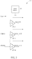
- FIG. 2 is a diagram illustrating the memory interface circuit 122 according to one embodiment of the present invention.
- the memory interface circuit 122 comprises a signal detector 210 and a plurality of receivers 220_1 -220_M.
- the signal detector 210 is connected to a clock pin of the memory module 120, and is arranged to detect whether the memory interface circuit 122 receives the clock signal CLK or not to generate a detection result SD to enable or disable the receivers 220_1-220_M.
- the signal detector 210 may detect whether a signal swing on the clock pin is greater than a threshold Vth or not to generate the detection result SD, that is if the signal swing is greater than the threshold Vth, the detection result SD has a higher voltage level to indicate that the memory interface circuit 122 receives the clock signal; and if the signal swing is lower than the threshold Vth, the detection result SD has a lower voltage level to indicate that the memory interface circuit 122 does not receive the clock signal.
- the signal detector 210 may comprise a hysteresis comparator to determine the clock signal, for example, if the signal swing is greater than a first threshold, the signal detector 210 starts to generate the detection result SD that has the higher voltage level; and if the signal swing is less than a second threshold different from the first threshold, the signal detector starts to generate the detection result that has the lower voltage level.
- the detection result SD is used to enable or disable the receivers 220_1-220_M.
- the detection result SD indicates that the memory interface circuit 122 receives the clock signal CLK
- the detection result SD enables the receivers 220_1-220_M; meanwhile, the receiver 220_1 receives the clock signal CLK to generate an output clock signal CLK_OUT to the control circuit 124, and the receiver 220_2-220_M receive the command signals CMD[1] - CMD[N] to generate output command signals CMD[1]_OUT - CMD[N]_OUT, respectively, to the control circuit 124.
- the detection result SD when the detection result SD indicates that the memory interface circuit 122 does not receive the clock signal CLK, the detection result SD disables the receivers 220_1-220_M, that is the receivers 220_1-220_M will not output the output clock signal CLK_OUT and the output command signals CMD[1]_OUT - CMD[N]_OUT to the control circuit 124, that is the control circuit 124 does not work to access the memory array 126.
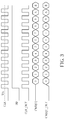
- FIG. 3 shows a timing diagram of some signals shown in FIG. 2 according to one embodiment of the present invention. It is noted that, in the embodiment shown in FIG. 3 , the output clock signal CLK_OUT is substantially equal to the clock signal CLK, and the command signal CMD[1] is substantially equal to the output command signal CMD[1]_OUT, however, this is not a limitation of the present invention. In another embodiment, the output clock signal CLK_OUT and the command signal CMD[1] may be generated to satisfy the logical requirements of the memory module 120.
- FIG. 4 is a flowchart of a control method of a memory interface circuit according to one embodiment of the present invention. Referring to FIGs. 1-4 and the aforementioned disclosure, the flow is described as follows.
- Step 400 the flow starts.
- Step 402 provide a plurality of receivers for receiving at least a clock signal and a plurality of command signals from a memory controller, respectively.
- Step 404 detect whether the memory interface circuit receives the clock signal or not? If yes, the flow enters Step 406; if not, the flow enters Step 408.
- Step 406 enable the receivers.
- Step 408 disable the receivers.
- the memory interface circuit uses a signal detector to detect whether the memory interface circuit receives a clock signal from a memory controller or not to generate a detection result, and the detection result is arranged to enable or disable a plurality of receivers. Therefore, the conventional clock enable (CKE) signal and the clock enable pin can be removed from the memory system, thereby the manufacturing cost may be lowered, and the memory designs can be more flexible.
- CKE clock enable
Landscapes
- Engineering & Computer Science (AREA)
- Microelectronics & Electronic Packaging (AREA)
- Computer Hardware Design (AREA)
- Databases & Information Systems (AREA)
- Dram (AREA)
- Memory System (AREA)
Abstract
Description
- A conventional dynamic random access memory (DRAM) module has many pins for receiving data signal, command signals, clock signals and a clock enable signal from a memory controller. In order to decrease the manufacturing cost, engineers always try to decrease quantity of pins. Therefore, how to remove one or more pins without influencing functions of the DRAM module is an important topic.
- It is therefore an objective of the present invention to provide a memory interface, which includes a signal detector for detecting whether a clock signal is existed to generate a detection result to enable or disable a plurality of receivers. By using the embodiments of the present invention, the conventional clock enable (CKE) pin can be removed from the memory controller and memory module.
- This is achieved by a memory interface circuit according to
claim 1, a memory system according to claim 8, and a method according to claim 14. The dependent claims pertain to corresponding further developments and improvements. - As will be seen more clearly from the detailed description following below, a memory interface circuit includes a plurality of receivers and a signal detector. The plurality of receivers are arranged for receiving at least a clock signal and a plurality of command signals from a memory controller, respectively. The signal detector is arranged for detecting whether the memory interface circuit receives the clock signal or not to generate a detection result to enable or disable the plurality of receivers.
- As will be seen more clearly from the detailed description following below, a memory system comprises a memory controller and a memory module, wherein the memory module comprises a memory interface circuit and a control circuit, and the memory interface comprises a plurality of receivers and a signal detector. The memory controller is arranged for generating at least a clock signal and a plurality of command signals. The plurality of receivers are arranged for receiving at least the clock signal and the plurality of command signals from the memory controller, respectively, to generate a plurality of output signals. The signal detector is arranged for detecting whether the memory interface receives the clock signal or not to generate a detection result to enable or disable the plurality of receivers. The control circuit is arranged for receiving plurality of output signals from the memory interface circuit to access a memory array within the memory module.
- As will be seen more clearly from the detailed description following below, a control method of a memory interface circuit is provided, wherein the memory interface circuit comprises a plurality of receivers for receiving at least a clock signal and a plurality of command signals from a memory controller, respectively, and the control method comprises: detecting whether the memory interface circuit receives the clock signal or not to generate a detection result to enable or disable the plurality of receivers.
- These and other objectives of the present invention will no doubt become obvious to those of ordinary skill in the art after reading the following detailed description of the preferred embodiment that is illustrated in the various figures and drawings.
-
-
FIG. 1 is a diagram illustrating a memory system according to one embodiment of the present invention. -
FIG. 2 is a diagram illustrating the memory interface circuit according to one embodiment of the present invention. -
FIG. 3 shows a timing diagram of some signals shown inFIG. 2 according to one embodiment of the present invention. -
FIG. 4 is a flowchart of a control method of a memory interface circuit according to one embodiment of the present invention. - Certain terms are used throughout the following description and claims to refer to particular system components. As one skilled in the art will appreciate, manufacturers may refer to a component by different names. This document does not intend to distinguish between components that differ in name but not function. In the following discussion and in the claims, the terms "including" and "comprising" are used in an open-ended fashion, and thus should be interpreted to mean "including, but not limited to ..." The terms "couple" and "couples" are intended to mean either an indirect or a direct electrical connection. Thus, if a first device couples to a second device, that connection may be through a direct electrical connection, or through an indirect electrical connection via other devices and connections.
- Please refer to
FIG. 1 , which is a diagram illustrating amemory system 100 according to one embodiment of the present invention. As shown inFIG. 1 , thememory system 100 comprises amemory controller 110 and amemory module 1 20 supplied by a supply voltage VDD, where thememory module 120 comprises amemory interface circuit 122, acontrol circuit 124 and amemory array 126. In this embodiment, thememory controller 110 and thememory module 120 are connected via a plurality of connection lines, where the connection lines are used to transmit at least a bi-directional data signal DQ, a bi-directional data strobe signal DQS, a plurality of command signals CMDs and a differential clock signal CLK. In addition, in this embodiment, thememory system 100 is a volatile memory system such as a DRAM system, that is thememory controller 110 is the DRAM memory controller, and thememory module 120 is a DRAM memory module. - When the
memory system 100 is implemented by the DRAM system the command signals may comprise at least a row address strobe, a column address strobe, and a write enable signal. In addition, the clock signal or the command signals shown inFIG. 1 can be single-directional or bi-directional. - In the operations of the
memory system 100, thememory controller 110 is arranged to receive a request from a host or a processor, and to transmit at least a portion of the data signal DQ, data strobe signal DQS, command signals CMDs and the clock signal CLK to access thememory module 120. In addition, thememory controller 110 may comprise associated circuits, such an address decoder, a processing circuit, a write/read buffer, a control logic and an arbiter, to perform the related operations. Thememory interface circuit 1 22 is arranged to receive the data signal DQ, data strobe signal DQS, command signals CMDs and the clock signal CLK from thememory controller 110, and to selectively output a plurality of output signals to thecontrol circuit 124 or not according to the received signals. Thecontrol circuit 124 may comprise a read/write controller, a row decoder and a column decoder, and thecontrol circuit 124 is arranged to receive the output signals from thememory interface circuit 1 22 to access thememory array 1 26. - In this embodiment, the
memory system 100 does not have a conventional clock enable (CKE) pin, and thememory interface circuit 122 is arranged to detect whether thememory interface circuit 122 receives the clock signal CLK or not to generate a detection result to enable or disable a plurality of receivers within thememory interface circuit 122. That is, if thememory interface circuit 122 receives the clock signal CLK from thememory controller 110, the receivers within thememory interface circuit 122 are enabled to generate the outputs to thecontrol circuit 124 according to the received signals; and if thememory interface circuit 122 does not receive the clock signal CLK or any other clock signal from thememory controller 110, the receivers within thememory interface circuit 122 are disabled, and thecontrol circuit 124 will not receive the related signals to access thememory array 126. - Because the embodiments of the present invention focus on the designs of the
memory interface circuit 122, detailed descriptions about the other elements are therefore omitted here. - Please refer to
FIG. 2 , which is a diagram illustrating thememory interface circuit 122 according to one embodiment of the present invention. As shown inFIG. 2 , thememory interface circuit 122 comprises asignal detector 210 and a plurality of receivers 220_1 -220_M. Thesignal detector 210 is connected to a clock pin of thememory module 120, and is arranged to detect whether thememory interface circuit 122 receives the clock signal CLK or not to generate a detection result SD to enable or disable the receivers 220_1-220_M. In this embodiment, thesignal detector 210 may detect whether a signal swing on the clock pin is greater than a threshold Vth or not to generate the detection result SD, that is if the signal swing is greater than the threshold Vth, the detection result SD has a higher voltage level to indicate that thememory interface circuit 122 receives the clock signal; and if the signal swing is lower than the threshold Vth, the detection result SD has a lower voltage level to indicate that thememory interface circuit 122 does not receive the clock signal. In another embodiment, thesignal detector 210 may comprise a hysteresis comparator to determine the clock signal, for example, if the signal swing is greater than a first threshold, thesignal detector 210 starts to generate the detection result SD that has the higher voltage level; and if the signal swing is less than a second threshold different from the first threshold, the signal detector starts to generate the detection result that has the lower voltage level. - The detection result SD is used to enable or disable the receivers 220_1-220_M. When the detection result SD indicates that the
memory interface circuit 122 receives the clock signal CLK, the detection result SD enables the receivers 220_1-220_M; meanwhile, the receiver 220_1 receives the clock signal CLK to generate an output clock signal CLK_OUT to thecontrol circuit 124, and the receiver 220_2-220_M receive the command signals CMD[1] - CMD[N] to generate output command signals CMD[1]_OUT - CMD[N]_OUT, respectively, to thecontrol circuit 124. In addition, when the detection result SD indicates that thememory interface circuit 122 does not receive the clock signal CLK, the detection result SD disables the receivers 220_1-220_M, that is the receivers 220_1-220_M will not output the output clock signal CLK_OUT and the output command signals CMD[1]_OUT - CMD[N]_OUT to thecontrol circuit 124, that is thecontrol circuit 124 does not work to access thememory array 126. -
FIG. 3 shows a timing diagram of some signals shown inFIG. 2 according to one embodiment of the present invention. It is noted that, in the embodiment shown inFIG. 3 , the output clock signal CLK_OUT is substantially equal to the clock signal CLK, and the command signal CMD[1] is substantially equal to the output command signal CMD[1]_OUT, however, this is not a limitation of the present invention. In another embodiment, the output clock signal CLK_OUT and the command signal CMD[1] may be generated to satisfy the logical requirements of thememory module 120. -
FIG. 4 is a flowchart of a control method of a memory interface circuit according to one embodiment of the present invention. Referring toFIGs. 1-4 and the aforementioned disclosure, the flow is described as follows. - Step 400: the flow starts.
- Step 402: provide a plurality of receivers for receiving at least a clock signal and a plurality of command signals from a memory controller, respectively.
- Step 404: detect whether the memory interface circuit receives the clock signal or not? If yes, the flow enters
Step 406; if not, the flow entersStep 408. - Step 406: enable the receivers.
- Step 408: disable the receivers.
- Briefly summarized, in the memory system of the present invention, the memory interface circuit uses a signal detector to detect whether the memory interface circuit receives a clock signal from a memory controller or not to generate a detection result, and the detection result is arranged to enable or disable a plurality of receivers. Therefore, the conventional clock enable (CKE) signal and the clock enable pin can be removed from the memory system, thereby the manufacturing cost may be lowered, and the memory designs can be more flexible.
- Those skilled in the art will readily observe that numerous modifications and alterations of the device and method may be made while retaining the teachings of the invention. Accordingly, the above disclosure should be construed as limited only by the metes and bounds of the appended claims.
Claims (15)
- A memory interface circuit (1 22), characterized by:a plurality of receivers (220_1-220_M), for receiving at least a clock signal and a plurality of command signals from a memory controller (110), respectively; anda signal detector (210), for detecting whether the memory interface circuit receives the clock signal or not to generate a detection result to enable or disable the plurality of receivers.
- The memory interface circuit (122) of claim 1, characterized in that when the detection result indicates that the memory interface circuit (122) receives the clock signal, the detection result enables the plurality of receivers (220_1-220_M); and when the detection result indicates that the memory interface circuit (122) does not receive the clock signal, the detection result disables the plurality of receivers (220_1 -220_M).
- The memory interface circuit (122) of claim 2, characterized in that when the detection result indicates that the memory interface circuit (122) receives the clock signal, the detection result enables the plurality of receivers (220_1-220_M) to receive the at least the clock signal and the plurality of command signals from the memory controller (110), and to generate an output clock signal and a plurality of output command signals to a control circuit (124) of a memory module (120), respectively; and when the detection result indicates that the memory interface circuit (122) does not receive the clock signal, the detection result disables the plurality of receivers (220_1-220_M) to not output any signal to the control circuit (1 24) of the memory module (1 20).
- The memory interface circuit (122) of claim 1, characterized in that the signal detector (210) detects a swing of the clock signal to generate the detection result.
- The memory interface circuit (122) of claim 4, characterized in that the signal detector (210) detects whether the swing of the clock signal is greater than a threshold or not to generate the detection result.
- The memory interface circuit (122) of claim 4, characterized in that when the swing of the clock signal is greater than a first threshold, the signal detector (210) starts to generate the detection result to enable the plurality of receivers (220_1-220_M); and when the swing of the clock signal is less than a second threshold, the signal detector (210) starts to generate the detection result to disable the plurality of receivers (220_1 -220_M).
- The memory interface circuit (122) of claim 1, characterized in that the memory interface circuit (122) is applied in a dynamic random access memory (DRAM).
- A memory system (100), comprising:a memory controller (110), for generating at least a clock signal and a plurality of command signals;characterized by:a memory module (1 20), comprising:a memory interface circuit (1 22), comprising:a plurality of receivers (220_1-220_M), for receiving at least the clock signal and the plurality of command signals from the memory controller (110), respectively, to generate a plurality of output signals; anda signal detector (210), for detecting whether the memory interface circuit (122) receives the clock signal or not to generate a detection result to enable or disable the plurality of receivers (220_1 -220_M); anda control circuit (1 24), for receiving plurality of output signals from the memory interface circuit (122) to access a memory array (126) within the memory module (120).
- The memory system (100) of claim 8, characterized in that when the detection result indicates that the memory interface circuit (122) receives the clock signal, the detection result enables the plurality of receivers (220_1-220_M); and when the detection result indicates that the memory interface circuit (122) does not receive the clock signal, the detection result disables the plurality of receivers (220_1 -220_M).
- The memory system (100) of claim 9, characterized in that when the detection result indicates that the memory interface circuit (122) receives the clock signal, the detection result enables the plurality of receivers (220_1-220_M) to receive the at least the clock signal and the plurality of command signals from the memory controller (110), and to generate the output signals comprising an output clock signal and a plurality of output command signals to the control circuit (124), respectively; and when the detection result indicates that the memory interface circuit (122) does not receive the clock signal, the detection result disables the plurality of receivers (220_1 -220_M) to not output any signal to the control circuit of the memory module (120).
- The memory system (100) of claim 8, characterized in that the signal detector (210) detects a swing of the clock signal to generate the detection result.
- The memory system (100) of claim 11, characterized in that the signal detector (210) detects whether the swing of the clock signal is greater than a threshold or not to generate the detection result.
- The memory system (100) of claim 12, characterized in that when the swing of the clock signal is greater than a first threshold, the signal detector (210) starts to generate the detection result to enable the plurality of receivers (220_1-220_M); and when the swing of the clock signal is less than a second threshold, the signal detector (210) starts to generate the detection result to disable the plurality of receivers (220_1 -220_M).
- A control method of a memory interface circuit (122), wherein the memory interface circuit (122) comprises a plurality of receivers (220_1 -220_M) for receiving at least a clock signal and a plurality of command signals from a memory controller (110), respectively, characterized by the method comprises the steps of:detecting whether the memory interface circuit (122) receives the clock signal or not to generate a detection result to enable or disable the plurality of receivers (220_1-220_M).
- The control method of claim 14, characterized in that the step of detecting whether the memory interface circuit (122) receives the clock signal or not to generate the detection result to enable or disable the plurality of receivers (220_1-220_M) comprises:when the detection result indicates that the memory interface circuit (122) receives the clock signal, the detection result enables the plurality of receivers (220_1-220_M); andwhen the detection result indicates that the memory interface circuit (122) does not receive the clock signal, the detection result disables the plurality of receivers (220_1-220_M).
Applications Claiming Priority (2)
| Application Number | Priority Date | Filing Date | Title |
|---|---|---|---|
| US201662289929P | 2016-02-02 | 2016-02-02 | |
| US15/247,870 US10141044B2 (en) | 2016-02-02 | 2016-08-25 | Memory interface circuit having signal detector for detecting clock signal |
Publications (2)
| Publication Number | Publication Date |
|---|---|
| EP3203476A1 true EP3203476A1 (en) | 2017-08-09 |
| EP3203476B1 EP3203476B1 (en) | 2019-10-30 |
Family
ID=56883588
Family Applications (1)
| Application Number | Title | Priority Date | Filing Date |
|---|---|---|---|
| EP16186784.1A Active EP3203476B1 (en) | 2016-02-02 | 2016-09-01 | Memory interface circuit having signal detector for detecting clock signal |
Country Status (3)
| Country | Link |
|---|---|
| US (1) | US10141044B2 (en) |
| EP (1) | EP3203476B1 (en) |
| CN (1) | CN107039066B (en) |
Families Citing this family (7)
| Publication number | Priority date | Publication date | Assignee | Title |
|---|---|---|---|---|
| US10586832B2 (en) | 2011-02-14 | 2020-03-10 | Attopsemi Technology Co., Ltd | One-time programmable devices using gate-all-around structures |
| US11062786B2 (en) | 2017-04-14 | 2021-07-13 | Attopsemi Technology Co., Ltd | One-time programmable memories with low power read operation and novel sensing scheme |
| US11615859B2 (en) | 2017-04-14 | 2023-03-28 | Attopsemi Technology Co., Ltd | One-time programmable memories with ultra-low power read operation and novel sensing scheme |
| US10504581B1 (en) * | 2018-06-26 | 2019-12-10 | Nanya Technology Corporation | Memory apparatus and operating method thereof |
| WO2020034985A1 (en) | 2018-08-14 | 2020-02-20 | Mediatek Inc. | Delay tracking method and memory system |
| US12483429B2 (en) | 2021-06-01 | 2025-11-25 | Attopsemi Technology Co., Ltd | Physically unclonable function produced using OTP memory |
| KR20240117196A (en) | 2023-01-25 | 2024-08-01 | 삼성전자주식회사 | Clock driver, operating method thereof, memory device including clock driver, and memory system |
Citations (7)
| Publication number | Priority date | Publication date | Assignee | Title |
|---|---|---|---|---|
| US20010043099A1 (en) * | 1998-01-21 | 2001-11-22 | Kenichi Kawasaki | Input circuit and semiconductor integrated circuti having the input circuit |
| US20040124887A1 (en) * | 2002-09-24 | 2004-07-01 | Andre Schaefer | Circuit device with clock pulse detection facility |
| US20070070782A1 (en) * | 2005-09-10 | 2007-03-29 | Dong-Woo Lee | Memory device input buffer, related memory device, controller and system |
| US20110032787A1 (en) * | 2009-08-07 | 2011-02-10 | Samsung Electronics Co., Ltd. | Input buffer circuit, semiconductor memory device and memory system |
| US20110126039A1 (en) * | 2009-11-20 | 2011-05-26 | Si-Hong Kim | Memory controller with reduced power consumption, memory device, and memory system |
| US20120120746A1 (en) * | 2010-11-15 | 2012-05-17 | Hynix Semiconductor Inc. | Semiconductor memory apparatus |
| US20150227188A1 (en) * | 2009-01-12 | 2015-08-13 | Rambus Inc. | Memory controller with transaction-queue-dependent power modes |
Family Cites Families (7)
| Publication number | Priority date | Publication date | Assignee | Title |
|---|---|---|---|---|
| JP4090088B2 (en) * | 1996-09-17 | 2008-05-28 | 富士通株式会社 | Semiconductor device system and semiconductor device |
| JP3211739B2 (en) * | 1997-08-25 | 2001-09-25 | 日本電気株式会社 | Semiconductor storage device |
| US7142478B2 (en) * | 2004-03-19 | 2006-11-28 | Infineon Technologies Ag | Clock stop detector |
| KR100612950B1 (en) * | 2004-04-22 | 2006-08-14 | 주식회사 하이닉스반도체 | DRAM's las-time control circuit and las-time control method using external clock |
| KR101132800B1 (en) * | 2010-06-09 | 2012-04-02 | 주식회사 하이닉스반도체 | Data input circuit |
| WO2012122381A2 (en) * | 2011-03-09 | 2012-09-13 | Rambus Inc. | Power-management for integrated circuits |
| US9871518B2 (en) * | 2016-02-02 | 2018-01-16 | Mediatek Inc. | Memory interface circuit capable of controlling driving ability and associated control method |
-
2016
- 2016-08-25 US US15/247,870 patent/US10141044B2/en active Active
- 2016-09-01 EP EP16186784.1A patent/EP3203476B1/en active Active
-
2017
- 2017-01-24 CN CN201710059797.6A patent/CN107039066B/en active Active
Patent Citations (7)
| Publication number | Priority date | Publication date | Assignee | Title |
|---|---|---|---|---|
| US20010043099A1 (en) * | 1998-01-21 | 2001-11-22 | Kenichi Kawasaki | Input circuit and semiconductor integrated circuti having the input circuit |
| US20040124887A1 (en) * | 2002-09-24 | 2004-07-01 | Andre Schaefer | Circuit device with clock pulse detection facility |
| US20070070782A1 (en) * | 2005-09-10 | 2007-03-29 | Dong-Woo Lee | Memory device input buffer, related memory device, controller and system |
| US20150227188A1 (en) * | 2009-01-12 | 2015-08-13 | Rambus Inc. | Memory controller with transaction-queue-dependent power modes |
| US20110032787A1 (en) * | 2009-08-07 | 2011-02-10 | Samsung Electronics Co., Ltd. | Input buffer circuit, semiconductor memory device and memory system |
| US20110126039A1 (en) * | 2009-11-20 | 2011-05-26 | Si-Hong Kim | Memory controller with reduced power consumption, memory device, and memory system |
| US20120120746A1 (en) * | 2010-11-15 | 2012-05-17 | Hynix Semiconductor Inc. | Semiconductor memory apparatus |
Also Published As
| Publication number | Publication date |
|---|---|
| CN107039066A (en) | 2017-08-11 |
| US20170221544A1 (en) | 2017-08-03 |
| CN107039066B (en) | 2020-08-28 |
| US10141044B2 (en) | 2018-11-27 |
| EP3203476B1 (en) | 2019-10-30 |
Similar Documents
| Publication | Publication Date | Title |
|---|---|---|
| US10141044B2 (en) | Memory interface circuit having signal detector for detecting clock signal | |
| KR102398586B1 (en) | Timing based arbiter systems and circuits for zq calibration | |
| US10163485B2 (en) | Memory module, memory controller and associated control method for read training technique | |
| US9812187B2 (en) | Termination topology of memory system and associated memory module and control method | |
| US20130003474A1 (en) | Providing a ready-busy signal from a non-volatile memory device to a memory controller | |
| US8576645B2 (en) | Semiconductor memory device capable of minimizing current consumption during high speed operation | |
| EP3203475A1 (en) | Memory interface circuit capable of controlling driving ability and associated control method | |
| US20100202180A1 (en) | Memory module cutting off dm pad leakage current | |
| KR102388247B1 (en) | Individually Addressing Memory Devices Separated from the Data Bus | |
| KR101959929B1 (en) | Termination topology of memory system and associated memory module and control method | |
| CN107301874A (en) | Refresh control device | |
| US20140063979A1 (en) | Semiconductor device and data output circuit therefor | |
| US10282289B2 (en) | Package modules and methods of testing operations of chips included therein | |
| US10037788B2 (en) | Semiconductor devices and semiconductor systems | |
| US9997222B1 (en) | Semiconductor devices | |
| US9773530B1 (en) | Semiconductor devices and semiconductor systems relating to the prevention of a potential difference between signals from being reversed | |
| US9583214B2 (en) | Semiconductor circuit and leakage current test system | |
| US10908211B2 (en) | Integrated circuit and detection method for multi-chip status thereof | |
| US10621039B2 (en) | Electronic devices | |
| US9990983B2 (en) | Memory control circuit unit, memory storage device and signal receiving method | |
| KR100338824B1 (en) | Test board of ddr synchronous dram | |
| US20180113613A1 (en) | Information receiving device and semiconductor device including the same |
Legal Events
| Date | Code | Title | Description |
|---|---|---|---|
| PUAI | Public reference made under article 153(3) epc to a published international application that has entered the european phase |
Free format text: ORIGINAL CODE: 0009012 |
|
| STAA | Information on the status of an ep patent application or granted ep patent |
Free format text: STATUS: THE APPLICATION HAS BEEN PUBLISHED |
|
| AK | Designated contracting states |
Kind code of ref document: A1 Designated state(s): AL AT BE BG CH CY CZ DE DK EE ES FI FR GB GR HR HU IE IS IT LI LT LU LV MC MK MT NL NO PL PT RO RS SE SI SK SM TR |
|
| AX | Request for extension of the european patent |
Extension state: BA ME |
|
| STAA | Information on the status of an ep patent application or granted ep patent |
Free format text: STATUS: REQUEST FOR EXAMINATION WAS MADE |
|
| 17P | Request for examination filed |
Effective date: 20171122 |
|
| RBV | Designated contracting states (corrected) |
Designated state(s): AL AT BE BG CH CY CZ DE DK EE ES FI FR GB GR HR HU IE IS IT LI LT LU LV MC MK MT NL NO PL PT RO RS SE SI SK SM TR |
|
| STAA | Information on the status of an ep patent application or granted ep patent |
Free format text: STATUS: EXAMINATION IS IN PROGRESS |
|
| 17Q | First examination report despatched |
Effective date: 20181026 |
|
| GRAP | Despatch of communication of intention to grant a patent |
Free format text: ORIGINAL CODE: EPIDOSNIGR1 |
|
| STAA | Information on the status of an ep patent application or granted ep patent |
Free format text: STATUS: GRANT OF PATENT IS INTENDED |
|
| INTG | Intention to grant announced |
Effective date: 20190705 |
|
| GRAS | Grant fee paid |
Free format text: ORIGINAL CODE: EPIDOSNIGR3 |
|
| GRAA | (expected) grant |
Free format text: ORIGINAL CODE: 0009210 |
|
| STAA | Information on the status of an ep patent application or granted ep patent |
Free format text: STATUS: THE PATENT HAS BEEN GRANTED |
|
| RIN1 | Information on inventor provided before grant (corrected) |
Inventor name: CHEN, SHANG-PIN Inventor name: HSIEH, BO-WEI Inventor name: CHAN, CHIA-YU |
|
| AK | Designated contracting states |
Kind code of ref document: B1 Designated state(s): AL AT BE BG CH CY CZ DE DK EE ES FI FR GB GR HR HU IE IS IT LI LT LU LV MC MK MT NL NO PL PT RO RS SE SI SK SM TR |
|
| REG | Reference to a national code |
Ref country code: GB Ref legal event code: FG4D |
|
| REG | Reference to a national code |
Ref country code: CH Ref legal event code: EP |
|
| REG | Reference to a national code |
Ref country code: AT Ref legal event code: REF Ref document number: 1197010 Country of ref document: AT Kind code of ref document: T Effective date: 20191115 |
|
| REG | Reference to a national code |
Ref country code: DE Ref legal event code: R096 Ref document number: 602016023219 Country of ref document: DE |
|
| REG | Reference to a national code |
Ref country code: IE Ref legal event code: FG4D |
|
| REG | Reference to a national code |
Ref country code: LT Ref legal event code: MG4D |
|
| PG25 | Lapsed in a contracting state [announced via postgrant information from national office to epo] |
Ref country code: NL Free format text: LAPSE BECAUSE OF FAILURE TO SUBMIT A TRANSLATION OF THE DESCRIPTION OR TO PAY THE FEE WITHIN THE PRESCRIBED TIME-LIMIT Effective date: 20191030 Ref country code: SE Free format text: LAPSE BECAUSE OF FAILURE TO SUBMIT A TRANSLATION OF THE DESCRIPTION OR TO PAY THE FEE WITHIN THE PRESCRIBED TIME-LIMIT Effective date: 20191030 Ref country code: PL Free format text: LAPSE BECAUSE OF FAILURE TO SUBMIT A TRANSLATION OF THE DESCRIPTION OR TO PAY THE FEE WITHIN THE PRESCRIBED TIME-LIMIT Effective date: 20191030 Ref country code: LT Free format text: LAPSE BECAUSE OF FAILURE TO SUBMIT A TRANSLATION OF THE DESCRIPTION OR TO PAY THE FEE WITHIN THE PRESCRIBED TIME-LIMIT Effective date: 20191030 Ref country code: BG Free format text: LAPSE BECAUSE OF FAILURE TO SUBMIT A TRANSLATION OF THE DESCRIPTION OR TO PAY THE FEE WITHIN THE PRESCRIBED TIME-LIMIT Effective date: 20200130 Ref country code: NO Free format text: LAPSE BECAUSE OF FAILURE TO SUBMIT A TRANSLATION OF THE DESCRIPTION OR TO PAY THE FEE WITHIN THE PRESCRIBED TIME-LIMIT Effective date: 20200130 Ref country code: GR Free format text: LAPSE BECAUSE OF FAILURE TO SUBMIT A TRANSLATION OF THE DESCRIPTION OR TO PAY THE FEE WITHIN THE PRESCRIBED TIME-LIMIT Effective date: 20200131 Ref country code: LV Free format text: LAPSE BECAUSE OF FAILURE TO SUBMIT A TRANSLATION OF THE DESCRIPTION OR TO PAY THE FEE WITHIN THE PRESCRIBED TIME-LIMIT Effective date: 20191030 Ref country code: PT Free format text: LAPSE BECAUSE OF FAILURE TO SUBMIT A TRANSLATION OF THE DESCRIPTION OR TO PAY THE FEE WITHIN THE PRESCRIBED TIME-LIMIT Effective date: 20200302 Ref country code: FI Free format text: LAPSE BECAUSE OF FAILURE TO SUBMIT A TRANSLATION OF THE DESCRIPTION OR TO PAY THE FEE WITHIN THE PRESCRIBED TIME-LIMIT Effective date: 20191030 |
|
| REG | Reference to a national code |
Ref country code: NL Ref legal event code: MP Effective date: 20191030 |
|
| PG25 | Lapsed in a contracting state [announced via postgrant information from national office to epo] |
Ref country code: RS Free format text: LAPSE BECAUSE OF FAILURE TO SUBMIT A TRANSLATION OF THE DESCRIPTION OR TO PAY THE FEE WITHIN THE PRESCRIBED TIME-LIMIT Effective date: 20191030 Ref country code: HR Free format text: LAPSE BECAUSE OF FAILURE TO SUBMIT A TRANSLATION OF THE DESCRIPTION OR TO PAY THE FEE WITHIN THE PRESCRIBED TIME-LIMIT Effective date: 20191030 Ref country code: IS Free format text: LAPSE BECAUSE OF FAILURE TO SUBMIT A TRANSLATION OF THE DESCRIPTION OR TO PAY THE FEE WITHIN THE PRESCRIBED TIME-LIMIT Effective date: 20200229 |
|
| PG25 | Lapsed in a contracting state [announced via postgrant information from national office to epo] |
Ref country code: AL Free format text: LAPSE BECAUSE OF FAILURE TO SUBMIT A TRANSLATION OF THE DESCRIPTION OR TO PAY THE FEE WITHIN THE PRESCRIBED TIME-LIMIT Effective date: 20191030 |
|
| PG25 | Lapsed in a contracting state [announced via postgrant information from national office to epo] |
Ref country code: RO Free format text: LAPSE BECAUSE OF FAILURE TO SUBMIT A TRANSLATION OF THE DESCRIPTION OR TO PAY THE FEE WITHIN THE PRESCRIBED TIME-LIMIT Effective date: 20191030 Ref country code: CZ Free format text: LAPSE BECAUSE OF FAILURE TO SUBMIT A TRANSLATION OF THE DESCRIPTION OR TO PAY THE FEE WITHIN THE PRESCRIBED TIME-LIMIT Effective date: 20191030 Ref country code: EE Free format text: LAPSE BECAUSE OF FAILURE TO SUBMIT A TRANSLATION OF THE DESCRIPTION OR TO PAY THE FEE WITHIN THE PRESCRIBED TIME-LIMIT Effective date: 20191030 Ref country code: DK Free format text: LAPSE BECAUSE OF FAILURE TO SUBMIT A TRANSLATION OF THE DESCRIPTION OR TO PAY THE FEE WITHIN THE PRESCRIBED TIME-LIMIT Effective date: 20191030 Ref country code: ES Free format text: LAPSE BECAUSE OF FAILURE TO SUBMIT A TRANSLATION OF THE DESCRIPTION OR TO PAY THE FEE WITHIN THE PRESCRIBED TIME-LIMIT Effective date: 20191030 |
|
| REG | Reference to a national code |
Ref country code: DE Ref legal event code: R097 Ref document number: 602016023219 Country of ref document: DE |
|
| REG | Reference to a national code |
Ref country code: AT Ref legal event code: MK05 Ref document number: 1197010 Country of ref document: AT Kind code of ref document: T Effective date: 20191030 |
|
| PG25 | Lapsed in a contracting state [announced via postgrant information from national office to epo] |
Ref country code: IT Free format text: LAPSE BECAUSE OF FAILURE TO SUBMIT A TRANSLATION OF THE DESCRIPTION OR TO PAY THE FEE WITHIN THE PRESCRIBED TIME-LIMIT Effective date: 20191030 Ref country code: SK Free format text: LAPSE BECAUSE OF FAILURE TO SUBMIT A TRANSLATION OF THE DESCRIPTION OR TO PAY THE FEE WITHIN THE PRESCRIBED TIME-LIMIT Effective date: 20191030 Ref country code: SM Free format text: LAPSE BECAUSE OF FAILURE TO SUBMIT A TRANSLATION OF THE DESCRIPTION OR TO PAY THE FEE WITHIN THE PRESCRIBED TIME-LIMIT Effective date: 20191030 |
|
| PLBE | No opposition filed within time limit |
Free format text: ORIGINAL CODE: 0009261 |
|
| STAA | Information on the status of an ep patent application or granted ep patent |
Free format text: STATUS: NO OPPOSITION FILED WITHIN TIME LIMIT |
|
| 26N | No opposition filed |
Effective date: 20200731 |
|
| PG25 | Lapsed in a contracting state [announced via postgrant information from national office to epo] |
Ref country code: AT Free format text: LAPSE BECAUSE OF FAILURE TO SUBMIT A TRANSLATION OF THE DESCRIPTION OR TO PAY THE FEE WITHIN THE PRESCRIBED TIME-LIMIT Effective date: 20191030 Ref country code: SI Free format text: LAPSE BECAUSE OF FAILURE TO SUBMIT A TRANSLATION OF THE DESCRIPTION OR TO PAY THE FEE WITHIN THE PRESCRIBED TIME-LIMIT Effective date: 20191030 |
|
| REG | Reference to a national code |
Ref country code: CH Ref legal event code: PL |
|
| REG | Reference to a national code |
Ref country code: BE Ref legal event code: MM Effective date: 20200930 |
|
| PG25 | Lapsed in a contracting state [announced via postgrant information from national office to epo] |
Ref country code: LU Free format text: LAPSE BECAUSE OF NON-PAYMENT OF DUE FEES Effective date: 20200901 |
|
| PG25 | Lapsed in a contracting state [announced via postgrant information from national office to epo] |
Ref country code: IE Free format text: LAPSE BECAUSE OF NON-PAYMENT OF DUE FEES Effective date: 20200901 Ref country code: LI Free format text: LAPSE BECAUSE OF NON-PAYMENT OF DUE FEES Effective date: 20200930 Ref country code: BE Free format text: LAPSE BECAUSE OF NON-PAYMENT OF DUE FEES Effective date: 20200930 Ref country code: CH Free format text: LAPSE BECAUSE OF NON-PAYMENT OF DUE FEES Effective date: 20200930 |
|
| PG25 | Lapsed in a contracting state [announced via postgrant information from national office to epo] |
Ref country code: TR Free format text: LAPSE BECAUSE OF FAILURE TO SUBMIT A TRANSLATION OF THE DESCRIPTION OR TO PAY THE FEE WITHIN THE PRESCRIBED TIME-LIMIT Effective date: 20191030 Ref country code: MT Free format text: LAPSE BECAUSE OF FAILURE TO SUBMIT A TRANSLATION OF THE DESCRIPTION OR TO PAY THE FEE WITHIN THE PRESCRIBED TIME-LIMIT Effective date: 20191030 Ref country code: CY Free format text: LAPSE BECAUSE OF FAILURE TO SUBMIT A TRANSLATION OF THE DESCRIPTION OR TO PAY THE FEE WITHIN THE PRESCRIBED TIME-LIMIT Effective date: 20191030 |
|
| PG25 | Lapsed in a contracting state [announced via postgrant information from national office to epo] |
Ref country code: MK Free format text: LAPSE BECAUSE OF FAILURE TO SUBMIT A TRANSLATION OF THE DESCRIPTION OR TO PAY THE FEE WITHIN THE PRESCRIBED TIME-LIMIT Effective date: 20191030 Ref country code: MC Free format text: LAPSE BECAUSE OF FAILURE TO SUBMIT A TRANSLATION OF THE DESCRIPTION OR TO PAY THE FEE WITHIN THE PRESCRIBED TIME-LIMIT Effective date: 20191030 |
|
| P01 | Opt-out of the competence of the unified patent court (upc) registered |
Effective date: 20230607 |
|
| REG | Reference to a national code |
Ref country code: DE Ref legal event code: R081 Ref document number: 602016023219 Country of ref document: DE Owner name: INTERLINK SILICON SOLUTIONS INC, CA Free format text: FORMER OWNER: MEDIATEK INC., HSIN-CHU, TW |
|
| PGFP | Annual fee paid to national office [announced via postgrant information from national office to epo] |
Ref country code: DE Payment date: 20250702 Year of fee payment: 10 |
|
| PGFP | Annual fee paid to national office [announced via postgrant information from national office to epo] |
Ref country code: GB Payment date: 20250703 Year of fee payment: 10 |
|
| PGFP | Annual fee paid to national office [announced via postgrant information from national office to epo] |
Ref country code: FR Payment date: 20250703 Year of fee payment: 10 |