EP3203282A1 - Rib type optical waveguide and optical multiplexer/demultiplexer using same - Google Patents
Rib type optical waveguide and optical multiplexer/demultiplexer using same Download PDFInfo
- Publication number
- EP3203282A1 EP3203282A1 EP15846939.5A EP15846939A EP3203282A1 EP 3203282 A1 EP3203282 A1 EP 3203282A1 EP 15846939 A EP15846939 A EP 15846939A EP 3203282 A1 EP3203282 A1 EP 3203282A1
- Authority
- EP
- European Patent Office
- Prior art keywords
- optical
- optical waveguide
- rib type
- mode
- demultiplexer
- Prior art date
- Legal status (The legal status is an assumption and is not a legal conclusion. Google has not performed a legal analysis and makes no representation as to the accuracy of the status listed.)
- Granted
Links
Images





Classifications
-
- G—PHYSICS
- G02—OPTICS
- G02B—OPTICAL ELEMENTS, SYSTEMS OR APPARATUS
- G02B6/00—Light guides; Structural details of arrangements comprising light guides and other optical elements, e.g. couplings
- G02B6/10—Light guides; Structural details of arrangements comprising light guides and other optical elements, e.g. couplings of the optical waveguide type
- G02B6/12—Light guides; Structural details of arrangements comprising light guides and other optical elements, e.g. couplings of the optical waveguide type of the integrated circuit kind
- G02B6/12007—Light guides; Structural details of arrangements comprising light guides and other optical elements, e.g. couplings of the optical waveguide type of the integrated circuit kind forming wavelength selective elements, e.g. multiplexer, demultiplexer
-
- G—PHYSICS
- G02—OPTICS
- G02B—OPTICAL ELEMENTS, SYSTEMS OR APPARATUS
- G02B6/00—Light guides; Structural details of arrangements comprising light guides and other optical elements, e.g. couplings
- G02B6/10—Light guides; Structural details of arrangements comprising light guides and other optical elements, e.g. couplings of the optical waveguide type
- G02B6/12—Light guides; Structural details of arrangements comprising light guides and other optical elements, e.g. couplings of the optical waveguide type of the integrated circuit kind
- G02B6/122—Basic optical elements, e.g. light-guiding paths
- G02B6/1228—Tapered waveguides, e.g. integrated spot-size transformers
-
- G—PHYSICS
- G02—OPTICS
- G02B—OPTICAL ELEMENTS, SYSTEMS OR APPARATUS
- G02B6/00—Light guides; Structural details of arrangements comprising light guides and other optical elements, e.g. couplings
- G02B6/10—Light guides; Structural details of arrangements comprising light guides and other optical elements, e.g. couplings of the optical waveguide type
- G02B6/12—Light guides; Structural details of arrangements comprising light guides and other optical elements, e.g. couplings of the optical waveguide type of the integrated circuit kind
- G02B6/122—Basic optical elements, e.g. light-guiding paths
-
- G—PHYSICS
- G02—OPTICS
- G02B—OPTICAL ELEMENTS, SYSTEMS OR APPARATUS
- G02B6/00—Light guides; Structural details of arrangements comprising light guides and other optical elements, e.g. couplings
- G02B6/10—Light guides; Structural details of arrangements comprising light guides and other optical elements, e.g. couplings of the optical waveguide type
- G02B6/12—Light guides; Structural details of arrangements comprising light guides and other optical elements, e.g. couplings of the optical waveguide type of the integrated circuit kind
- G02B6/122—Basic optical elements, e.g. light-guiding paths
- G02B6/125—Bends, branchings or intersections
-
- G—PHYSICS
- G02—OPTICS
- G02B—OPTICAL ELEMENTS, SYSTEMS OR APPARATUS
- G02B6/00—Light guides; Structural details of arrangements comprising light guides and other optical elements, e.g. couplings
- G02B6/24—Coupling light guides
- G02B6/26—Optical coupling means
- G02B6/28—Optical coupling means having data bus means, i.e. plural waveguides interconnected and providing an inherently bidirectional system by mixing and splitting signals
- G02B6/2804—Optical coupling means having data bus means, i.e. plural waveguides interconnected and providing an inherently bidirectional system by mixing and splitting signals forming multipart couplers without wavelength selective elements, e.g. "T" couplers, star couplers
- G02B6/2808—Optical coupling means having data bus means, i.e. plural waveguides interconnected and providing an inherently bidirectional system by mixing and splitting signals forming multipart couplers without wavelength selective elements, e.g. "T" couplers, star couplers using a mixing element which evenly distributes an input signal over a number of outputs
- G02B6/2813—Optical coupling means having data bus means, i.e. plural waveguides interconnected and providing an inherently bidirectional system by mixing and splitting signals forming multipart couplers without wavelength selective elements, e.g. "T" couplers, star couplers using a mixing element which evenly distributes an input signal over a number of outputs based on multimode interference effect, i.e. self-imaging
-
- G—PHYSICS
- G02—OPTICS
- G02B—OPTICAL ELEMENTS, SYSTEMS OR APPARATUS
- G02B6/00—Light guides; Structural details of arrangements comprising light guides and other optical elements, e.g. couplings
- G02B6/24—Coupling light guides
- G02B6/26—Optical coupling means
- G02B6/28—Optical coupling means having data bus means, i.e. plural waveguides interconnected and providing an inherently bidirectional system by mixing and splitting signals
- G02B6/293—Optical coupling means having data bus means, i.e. plural waveguides interconnected and providing an inherently bidirectional system by mixing and splitting signals with wavelength selective means
- G02B6/29344—Optical coupling means having data bus means, i.e. plural waveguides interconnected and providing an inherently bidirectional system by mixing and splitting signals with wavelength selective means operating by modal interference or beating, i.e. of transverse modes, e.g. zero-gap directional coupler, MMI
-
- G—PHYSICS
- G02—OPTICS
- G02B—OPTICAL ELEMENTS, SYSTEMS OR APPARATUS
- G02B6/00—Light guides; Structural details of arrangements comprising light guides and other optical elements, e.g. couplings
- G02B6/24—Coupling light guides
- G02B6/26—Optical coupling means
- G02B6/28—Optical coupling means having data bus means, i.e. plural waveguides interconnected and providing an inherently bidirectional system by mixing and splitting signals
- G02B6/293—Optical coupling means having data bus means, i.e. plural waveguides interconnected and providing an inherently bidirectional system by mixing and splitting signals with wavelength selective means
- G02B6/29379—Optical coupling means having data bus means, i.e. plural waveguides interconnected and providing an inherently bidirectional system by mixing and splitting signals with wavelength selective means characterised by the function or use of the complete device
- G02B6/2938—Optical coupling means having data bus means, i.e. plural waveguides interconnected and providing an inherently bidirectional system by mixing and splitting signals with wavelength selective means characterised by the function or use of the complete device for multiplexing or demultiplexing, i.e. combining or separating wavelengths, e.g. 1xN, NxM
-
- H—ELECTRICITY
- H04—ELECTRIC COMMUNICATION TECHNIQUE
- H04B—TRANSMISSION
- H04B10/00—Transmission systems employing electromagnetic waves other than radio-waves, e.g. infrared, visible or ultraviolet light, or employing corpuscular radiation, e.g. quantum communication
- H04B10/40—Transceivers
-
- G—PHYSICS
- G02—OPTICS
- G02B—OPTICAL ELEMENTS, SYSTEMS OR APPARATUS
- G02B6/00—Light guides; Structural details of arrangements comprising light guides and other optical elements, e.g. couplings
- G02B6/10—Light guides; Structural details of arrangements comprising light guides and other optical elements, e.g. couplings of the optical waveguide type
- G02B6/12—Light guides; Structural details of arrangements comprising light guides and other optical elements, e.g. couplings of the optical waveguide type of the integrated circuit kind
- G02B2006/12083—Constructional arrangements
- G02B2006/12097—Ridge, rib or the like
-
- G—PHYSICS
- G02—OPTICS
- G02B—OPTICAL ELEMENTS, SYSTEMS OR APPARATUS
- G02B6/00—Light guides; Structural details of arrangements comprising light guides and other optical elements, e.g. couplings
- G02B6/10—Light guides; Structural details of arrangements comprising light guides and other optical elements, e.g. couplings of the optical waveguide type
- G02B6/12—Light guides; Structural details of arrangements comprising light guides and other optical elements, e.g. couplings of the optical waveguide type of the integrated circuit kind
- G02B2006/12133—Functions
- G02B2006/12164—Multiplexing; Demultiplexing
Definitions
- an optical switch element using a semiconductor-based optical waveguide capable of significantly miniaturizing an optical waveguide element.
- a silicon photonics technology As one of the technologies related to the optical switch element using the semiconductor-based optical waveguide, there is a silicon photonics technology.
- Signal light inputted to the matrix optical switch is scattered when passing through an intersection region, so that loss occurs.
- the degree of the scattering correlates with a ratio of the size of a section of the optical waveguide and the size (a mode diameter) of a basic propagation mode of the signal light.
- the influence of the scattering of the signal light in the intersection region appears notably.
- the cross section shape of the waveguide core is asymmetric.
- the propagation characteristics of the respective E x 11 mode and the E y 11 mode are generally different from each other and represent polarization dependence.
- the polarization dependence can be cancelled at a specific wavelength by optimally designing the sectional shape, but is difficult to be cancelled over a wide wavelength band.
- an optical multiplexer/demultiplexer or a tapered optical waveguide input part has a sectional shape different from that of an input/output optical waveguide.
- an optical multiplexer/demultiplexer includes M input optical waveguides and N output optical waveguides including a single mode rib type optical waveguide, reversible tapered regions that smoothly connect the input optical waveguides and the output optical waveguides to multi-mode optical interference regions and include MxN rib type optical waveguides, and the aforementioned rib type optical waveguide, wherein the input optical waveguides, the output optical waveguides, the multi-mode optical interference regions, and the reversible tapered regions are formed on a substrate.
- a 2x2 MMI optical multiplexer/demultiplexer 100 includes a SOI substrate (SOI: Semiconductor-on-Insulator) 200, input optical waveguides 300a and 300b, output optical waveguides 400a and 400b, tapered optical waveguides 500a, 500b, 500c, and 500d, and a rib type MMI region 600.
- SOI substrate SOI: Semiconductor-on-Insulator
- the input optical waveguides 300a and 300b, the output optical waveguides 400a and 400b, and the tapered optical waveguides 500a, 500b, 500c, and 500d are simply written as the input optical waveguide 300, the output optical waveguide 400, and the tapered optical waveguide 500 when it is not necessary to particularly distinguish them from another.
- the input optical waveguides 300a and 300b are straight semiconductor rib regions, are formed in regions of one end side of the SOI layer 230 of the SOI substrate 200, and form single mode optical waveguides of a pair of input sides.
- Optical signals inputted to the input optical waveguides 300a and 300b are inputted to the rib type MMI region 600 via the continuous tapered optical waveguides 500a and 500b.
- the tapered optical waveguide 500c smoothly connects the output optical waveguide 400a to the MMI part 610 of the rib type MMI region 600
- the tapered optical waveguide 500d smoothly connects the output optical waveguide 400b to the MMI part 610.
- the rib type MMI region 600 includes a semiconductor and allows an optical signal inputted from the input optical waveguide 300a via the tapered optical waveguides 500a to interfere with an optical signal inputted from the input optical waveguide 300b via the tapered optical waveguides 500b. Then, the rib type MMI region 600 outputs the interfered optical signal to the output optical waveguides 400a and 400b via the tapered optical waveguides 500c and 500d.
- thin stepped parts with a finite width are formed at both sidewalls extending in a direction (hereinafter, written as a longitudinal direction) toward the output optical waveguide 400 from the input optical waveguide 300.
- Fig. 2A and Fig. 2B illustrate a difference n 11 -n 12 (hereinafter, an effective refractive index difference) of a unique value (an effective refractive index n 11 ) of a basic mode and a unique value (an effective refractive index n 12 ) of a first high order mode of the rib type MMI region 600 when the sectional shapes of the narrow width stepped parts 620a and 620b are changed in the 2x2 MMI optical multiplexer/demultiplexer 100 configured as above.
- an effective refractive index difference of a unique value (an effective refractive index n 11 ) of a basic mode and a unique value (an effective refractive index n 12 ) of a first high order mode of the rib type MMI region 600 when the sectional shapes of the narrow width stepped parts 620a and 620b are changed in the 2x2 MMI optical multiplexer/demultiplexer 100 configured as above.
- the effective refractive index difference is inversely proportional to an interference cycle (a beat length) of the basic mode and the first high order mode in the rib type MMI region 600, and is an important parameter for deciding an optimal length of the rib type MMI region 600.
- a subscript of the effective refractive index difference n is written using a sign E of an electric field, but has the same meaning as that of the notation in the present specification.
- silicon a refractive index 3.48
- SiO 2 a refractive index 1.447
- a signal light wavelength is assumed to 1,550 nm.
- a width of the MMI part 610 is 7 ⁇ m
- a rib height is 0.9 ⁇ m
- a slab thickness is 0.6 ⁇ m.
- the ratio of polarization of the effective refractive index differences monotonically decreases as the widths w and the heights h of the narrow width stepped parts 620a and 620b increase.
- the ratio is 1, the optimal lengths of each polarization in the rib type MMI region 600 coincide with each other, that is, when it is assumed that there is no influence of the input/output optical waveguide, it is probable that it is possible to perform a polarization independent operation of the 2x2 MMI optical multiplexer/demultiplexer.
- the curvature of the equiphase surface (the wave front) is considered as an amount proportional to a propagation distance, and when the lengths of the tapered optical waveguides 500a, 500b, 500c, and 500d are sufficiently long compared to a wavelength, the signal light shows a behavior approximate to a plane wave.
- the lengths of the tapered optical waveguides 500a, 500b, 500c, and 500d are increased (as the tapered width is gently changed), while the loss (mode conversion loss) due to a mode shape change is suppressed, the loss due to optical absorption or scattering is increased.
- the equiphase surface (the wave front) of an electromagnetic field distribution of signal light to be propagated is kept to be curved.
- signal light is not excited with a plane wave, but is excited in the state in which the equiphase surface (the wave front) has been distorted. This causes finite loss and polarization dependence is shown in the loss itself.
- the fact that the 2x2 MMI optical multiplexer/demultiplexer 100 including the tapered optical waveguides 500a, 500b, 500c, and 500d and the rib type MMI region 600 performs a polarization independent operation is separately confirmed through electromagnetic field analysis.
- the heights h and the widths w of the narrow width stepped parts 620a and 620b are substantially inversely proportional to each other. Accordingly, when the areas of the narrow width stepped parts 620a and 620b are equal to each other, it is considered that optical multiplexing and demultiplexing characteristics also show almost the same tendency. However, as the widths w of the narrow width stepped parts 620a and 620b are widened, radiation to a slab region extending outward is promoted, resulting in an increase in insertion loss.
- the widths w of the narrow width stepped parts 620a and 620b are approximately equal to the signal light wavelength of the core material.
- the sectional shapes of the narrow width stepped parts 620a and 620b can also be formed in a right angled triangle for example.
- a rib sidewall is inclined from a surface vertical to the substrate.
- the rib sidewalls of the input optical waveguide 300, the output optical waveguide 400, and the tapered optical waveguide 500 are also inclined.
- the electromagnetic field distributions of the basic modes of the input optical waveguide 300 and the output optical waveguide 400 deviate from an assumed shape, so that design of polarization independence becomes difficult. Accordingly, it is practical that the sectional shapes of the narrow width stepped parts 620a and 620b are rectangular.
- the operation of the 2x2 MMI optical multiplexer/demultiplexer 100 described in the first example embodiment will be described.
- the insulating film 220 including a SiO 2 film with a thickness of 3 ⁇ m and the SOI layer 230 serving as a semiconductor layer with a thickness of 1.5 ⁇ m are arranged on the substrate 210, so that the SOI substrate 200 is formed.
- optical waveguide patterns are high precisely formed in the SOI layer 230 on the SOI substrate 200 by using a photolithography technology, so that the 2x2 MMI optical multiplexer/demultiplexer 100 described in the first example embodiment is formed.
- the aforementioned input optical waveguide 300 and the output optical waveguide 400, and the aforementioned rib type MMI region 600 are smoothly connected to each other by the tapered optical waveguide 500 (a reversible horizontal tapered region) having a length of 50 ⁇ m in which a rib height is 0.9 ⁇ m, a slab thickness is 0.6 ⁇ m, and a width is linearly changed from 1.4 ⁇ m to 3 ⁇ m.
- the tapered optical waveguide 500 a reversible horizontal tapered region having a length of 50 ⁇ m in which a rib height is 0.9 ⁇ m, a slab thickness is 0.6 ⁇ m, and a width is linearly changed from 1.4 ⁇ m to 3 ⁇ m.
- CMOS process such as high precision photolithography using a reduction projection exposure device using ArF in a light source and a phase shift mask, and a low damage dry etching technology.
- a previously stepped SiN film (not illustrated because it is removed in a manufacturing process) is provided as an etching blocking layer to be provided to the surface of the SOI substrate 200, so that the MMI part 610 and the narrow width stepped parts 620a and 620b at both sides thereof are integrally formed with each other in a one-time dry etching process.
- the transmittance for the E x mode of the 2x2 MMI optical multiplexer/demultiplexer 100 formed as described above is illustrated in Fig. 4
- a ratio (that is, polarization dependence of transmittance) of the transmittance for the E x mode and the transmittance for the E y mode is illustrated in Fig. 5 .
- a horizontal axis denotes the width of a tapered end portion (a wide side being in contact with the MMI part 610) of the tapered optical waveguide 500
- a vertical axis denotes the length of the rib type MMI region 600.
- a signal light wavelength is 1,590 nm.
- the transmittance is defined by Equation 1 below. 10 log P bar + P cross / P in unit : dB
- P bar denotes power outputted to a port (a bar output port) of the output optical waveguide 400 in front of signal light with power P in travelling straight from one side of the input optical waveguide 300
- P cross denotes power outputted to a port (a cross output port) of the output optical waveguide 400 in front of a diagonal line of the MMI part 610.
- the width and the MMI length dependence of a tapered end portion of insertion loss for the E x mode form a track-like contour line group in which a size differs step by step.
- the maximum value (the minimum value of the insertion loss) of the transmittance is -0.04 dB to -0.06 dB (+0.04 dB to +0.06 dB), so that a favorable value can be obtained for a 2x2 optical multiplexer/demultiplexer for a 1.5 ⁇ m band using Si as an optical waveguide core material.
- the transmittance for the E x mode is calculated (not illustrated). From the result, the length of the MMI part 610 of the 2x2 MMI optical multiplexer/demultiplexer 100 is set to 232 ⁇ m and the width of the tapered end portion is set to 3.3 ⁇ m.
- the 2x2 MMI optical multiplexer/demultiplexer 100 designed as described above has practical signal light branching characteristics in the signal light wavelength from 1,570 nm to 1,610 nm in configuring a matrix optical switch even though it is a rib type optical waveguide using the Si core whose section is not a square.
- the E x mode is from 0.08 dB to 0.09 dB
- the E y mode is from 0.07 dB to 0.08 dB
- polarization dependence loss is ⁇ 0.01 dB or less.
- the rib type MMI region 600 in which the narrow width stepped parts 620a and 620b are arranged at both sidewalls extending in the longitudinal direction of the MMI part 610, can be arranged in a ROADM (reconfigurable optical add/drop multiplexer), a 90 ° hybrid, an ADM matrix switch and the like, in addition to the MMI optical multiplexer/demultiplexer.
- ROADM reconfigurable optical add/drop multiplexer
- Si is used as a core material; however, it is possible to expect similar effects even in the case of using dielectric substances other than Si as a core. Furthermore, since it is not proper to use the SOI substrate 200 in the case of compound semiconductors and the like, optical confinement in a lamination direction (a direction vertical to a substrate) is reduced. However, also in this case, since a design concept is applicable, it is sufficient if a process of applying a proper perturbation to a sectional shape is performed in order to suppress polarization dependence of an effective refractive index difference at both sides of the MMI region. Moreover, the number of each of the input/output optical waveguides is not limited to 2, and the input/output optical waveguides can be applied to a M input N output (M ⁇ N) MMI optical multiplexer/demultiplexer.
- M ⁇ N MMI optical multiplexer/demultiplexer
Landscapes
- Physics & Mathematics (AREA)
- General Physics & Mathematics (AREA)
- Optics & Photonics (AREA)
- Engineering & Computer Science (AREA)
- Microelectronics & Electronic Packaging (AREA)
- Power Engineering (AREA)
- Electromagnetism (AREA)
- Computer Networks & Wireless Communication (AREA)
- Signal Processing (AREA)
- Optical Integrated Circuits (AREA)
Abstract
Description
- The present invention relates to a rib type optical waveguide and an optical multiplexer/demultiplexer using the same, and more particularly, to a rib type optical waveguide using a semiconductor-based optical waveguide and an optical multiplexer/demultiplexer using the same.
- With an explosive increase in the demand for a wideband multimedia communication service of the Internet, video distribution and the like, a long distant and highly reliable high density wavelength multiplexing optical fiber communication system has been introduced in a trunk line system or a metro system.
- In such a large scale communication network, the reduction of operational cost is important as well as the reduction of capital cost. In order to reduce the operational cost, it is needed to optimize dynamic transmission capacity allocation and path switching corresponding to demands, efficient maintenance, a redundant configuration and the like. That is, it is desired to be able to flexibly reconfigure a communication network, and is also desired to reduce cost of reconfiguration.
- In order to flexibly reconfigure the communication network at a low cost, an optical switch node capable of switching the path of light without converting a light signal into an electrical signal can be applied. Since the flexibility of the communication network depends on the degree of freedom of the path switching in the optical switch node, it is desired to provide an optical switch with a large number of ports.
- In the optical switch, it is further needed to suppress the loss of signal light passing through the optical switch, wavelength dependence, polarization dependence, crosstalk to a non-connection path, and the like. Furthermore, suppression of power consumption needed for holding and switching of a signal light path, and miniaturization of an optical switch node are also important. These are issues directly related to the expandability of the number of ports of the optical switch, and the reduction in size, low loss, and low power characteristics are needed for the optical switch.
- On the other hand, it is needed to suppress the occurrence of a problem related to communication service quality such as interruption of a line during communication, and to provide a stable communication state. Furthermore, a high speed path switching characteristic is also needed in order to prevent a line interruption state due to path switching from being recognized by a user. It is desired that such high speed switching can be performed in a small scale circuit with low power as much as possible.
- As such an optical switch, there are an MEMS (Micro Electro Mechanical Systems) matrix optical switch, a liquid crystal matrix optical switch, a waveguide matrix optical switch and the like. The MEMS matrix optical switch is an optical switch that switches an optical path of spatial propagation beams by electrostatically controlling the direction of fine movable mirrors formed on a silicon substrate. The liquid crystal matrix optical switch is an optical switch that controls transmittance of spatial propagation beams by electrically changing the alignment state of liquid crystal molecules. The waveguide matrix optical switch is an optical switch that selects a signal light output path by changing an interference state by using temperature dependence of a refractive index of an optical material constituting a waveguide type optical interferometer.
- The MEMS matrix optical switch is advantageous in terms of expandability of the number of input/output ports because insertion loss and signal light crosstalk are small. However, since about milliseconds are needed for a response of the movable mirror, the MEMS matrix optical switch is not suitable for use purposes needing high speed and high frequent path switching such as an uninterrupted optical path switching and optical packet signal switching. Furthermore, in the MEMS matrix optical switch, in the case of creating one input multi-output connection state, it is necessary to adjust a beam divergence angle in response to a distance between signal light output ports by sacrificing optical characteristics.
- The liquid crystal matrix optical switch has a response time constant equal to that of the MEMS matrix optical switch. The liquid crystal matrix optical switch has high mechanical reliability because it has no movable part such as MEMS. However, in the liquid crystal matrix optical switch, since optical characteristics of liquid crystal molecules largely depend on temperature, degeneration and deterioration may occur in a high temperature environment. Accordingly, in the liquid crystal matrix optical switch, it is necessary to consider resistance to environment and reliability when it is actually applied to a system.
- The waveguide matrix optical switch changes an interference state of a large number of waveguide optical interferometers formed on a substrate by electric field application, current injection, temperature and the like, thereby selecting an optical signal output path. The waveguide matrix optical switch is suitable for miniaturization as compared with the aforementioned two types of optical switch elements. Particularly, a waveguide matrix optical switch using silica is advantageous in terms of low loss because coupling efficiency with a single mode optical fiber is high. Furthermore, the waveguide matrix optical switch using silica has high mass productivity and reliability.
- The basis configuration of the waveguide matrix optical switch is an optical gate switch that thermally controls interference conditions of the waveguide optical interferometers by applying temperature dependence (a thermo-optic effect) of a refractive index of an optical waveguide material.
- A time (about milliseconds) approximately equal to that of the MEMS matrix optical switch is required in order such that heat transfer between a core and a clad/a substrate reaches equilibrium. Accordingly, in the waveguide matrix optical switch, in order to shorten the time needed for reaching heat equilibrium, it is desired to make a volume (a sectional area of an optical waveguide) of a heated area in the optical gate switch as small as possible.
- Under such situations, much attention has been attracted on an optical switch element using a semiconductor-based optical waveguide capable of significantly miniaturizing an optical waveguide element. As one of the technologies related to the optical switch element using the semiconductor-based optical waveguide, there is a silicon photonics technology. In the silicon photonics technology, a silicon film (SOI: Silicon On Insulator) formed on an insulating film (a film obtaining by thermally oxidizing a silicon substrate surface) is processed into a stripe shape and allowed to serve as an optical waveguide core. Since a refractive index difference between a core layer (a refractive index: about 3.48@1550nm) including the SOI film and a clad layer (a refractive index: about 1.45@1550nm) including a dielectric film (SiO2 and the like) is large, signal light is strongly confined into the core layer. Accordingly, when the silicon photonics technology is applied, it is possible to suppress insertion loss within a practical range even in a steep curve equal to or less than a curvature of 100 µm. Furthermore, in the silicon photonics technology, it is possible to expect high precision processing and mass productivity based on an advanced CMOS (Complementary Metal Oxide Semiconductor) process technology, and moreover, it is also possible to expect monolithic integration and the like with a driving circuit.
- In the case of implementing an M input N output (hereinafter, MxN: M and N are natural numbers equal to or more than 2) matrix optical switch by using the silicon photonics technology, a MxN waveguide optical switch is arranged on two-dimensional lattice points on a semiconductor substrate and optical waveguide groups for connecting them lengthwise and breadthwise are arranged on the same semiconductor substrate. In this case, the optical waveguide groups mutually intersect on the semiconductor substrate.
- Signal light inputted to the matrix optical switch is scattered when passing through an intersection region, so that loss occurs. The degree of the scattering correlates with a ratio of the size of a section of the optical waveguide and the size (a mode diameter) of a basic propagation mode of the signal light. Herein, in an optical waveguide using the silicon photonics technology, in which the refractive index difference between the core layer and the clad layer is high and optical confinement is strong, the influence of the scattering of the signal light in the intersection region appears notably. On the other hand, in an optical waveguide based on silica and the like in which the refractive index difference between the core and the clad is small and optical confinement is weak (a weak guided wave: weakly guiding), since the signal light shows a behavior approximate to a plane wave, it is less scattered when passing through the intersection region.
- In this regard, in order to reduce the influence of the scattering of the signal light in the intersection region, it has been proposed that a matrix optical switch using the silicon photonics technology is configured using a rib type optical waveguide formed by thickening a part of a two-dimensional thin slab optical waveguide.
- An electromagnetic field of a basic propagation mode of the rib type optical waveguide shows a sectional distribution of being approximately confined at inside (inside a silicon layer) than a refractive index boundary surface between a rib sidewall and the clad layer. Since it is possible to increase an effective sectional area by 1 digit as compared with a silicon wire, it is possible to allow signal light to propagate along the rib without taking into consideration of the refractive index boundary surface between the rib sidewall and the clad layer. In this case, it is possible to reduce the scattering of the signal light in the intersection region of the optical waveguide. A rib type optical waveguide-based optical switch element to which the silicon photonics technology is applied, for example, is disclosed in
PTLs 1 and 2 and the like. Furthermore, there has also been reported a development example of a matrix optical switch using a 2 input 2 output (2x2) MMI (Multi-Mode Interference) optical multiplexer/demultiplexer based on the rib type optical waveguide to which the silicon photonics technology is applied. Moreover, a technology related to the optical waveguide is disclosed in PTL 3. -
- [PTL 1] Japanese Unexamined Patent Application Publication No.
2001-183710 - [PTL 2] Japanese National Publication of International Patent Application No.
2002-514783 - [PTL 3] Japanese Unexamined Patent Application Publication No.
4-247408 - As described above, in designing a matrix optical switch to be applied to a trunk line system where optical fiber communication network systems with wavelength division multiplexing scheme is employed, wavelength independence and polarization independence are required. In a silica-based optical waveguide and a silicon wire, it is general to form a sectional shape of a core layer in a square shape in order to allow an electromagnetic field distribution of the core layer to approximate to an electromagnetic field distribution of a complete round of an optical fiber and to enhance the coupling efficiency of both. In the case of the square core layer, unique values (effective refractive indexes) of respective mode (an Ex 11 mode and a TE-like mode) parallel to a substrate and a mode (an Ey 11 mode and a TM-like mode) vertical to the substrate are degenerated. Since respective propagation characteristics are the same and are not distinguished from each other, there is no polarization dependence.
- On the other hand, in the case of the rib type optical waveguide in which the scattering in the intersection region of the optical waveguide is small, the cross section shape of the waveguide core is asymmetric. The propagation characteristics of the respective Ex 11 mode and the Ey 11 mode are generally different from each other and represent polarization dependence. The polarization dependence can be cancelled at a specific wavelength by optimally designing the sectional shape, but is difficult to be cancelled over a wide wavelength band. Moreover, in the case of the matrix optical switch, an optical multiplexer/demultiplexer or a tapered optical waveguide input part has a sectional shape different from that of an input/output optical waveguide. Since these polarization dependence and wavelength dependence are different from those of the input/output optical waveguide, it is not easy to find shape parameters for applying optimal polarization dependence and wavelength dependence. Moreover, even when the optimal shape parameters have been found, mass productivity and stable manufacturing yield are not always obtained.
- The present invention has been made in view of the aforementioned problems, and an object of the present invention is to provide a practical rib type optical waveguide in which polarization dependence and wavelength dependence and the like are small, and an optical multiplexer/demultiplexer using the same.
- In order to achieve the aforementioned object, a rib type optical waveguide according to the present invention includes a substrate, and a multi-mode optical interference region including a rib type optical waveguide formed on an upper surface of the substrate, wherein both side surfaces of the multi-mode optical interference region are respectively formed in a stepped shape.
- In order to achieve the aforementioned object, an optical multiplexer/demultiplexer according to the present invention includes M input optical waveguides and N output optical waveguides including a single mode rib type optical waveguide, reversible tapered regions that smoothly connect the input optical waveguides and the output optical waveguides to multi-mode optical interference regions and include MxN rib type optical waveguides, and the aforementioned rib type optical waveguide, wherein the input optical waveguides, the output optical waveguides, the multi-mode optical interference regions, and the reversible tapered regions are formed on a substrate.
- According to the aspects of the aforementioned present invention, it is possible to provide a practical rib type optical waveguide in which polarization dependence and wavelength dependence and the like are small, and an optical multiplexer/demultiplexer using the same.
-
-
Fig. 1A is a perspective view of a 2x2 MMI optical multiplexer/demultiplexer 100 according to a first example embodiment. -
Fig. 1B is a sectional view of a 2x2 MMI optical multiplexer/demultiplexer 100 according to a first example embodiment which is taken along line A-A'. -
Fig. 2A is a diagram illustrating a change in an effective refractive index difference in an Ex mode when sectional shapes of narrow width steppedparts demultiplexer 100 according to a first example embodiment. -
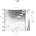
Fig. 2B is a diagram illustrating a change in an effective refractive index difference in an Ey mode when sectional shapes of narrow width steppedparts demultiplexer 100 according to a first example embodiment. -
Fig. 3 is a diagram plotting the ratio of effective refractive index differences of an Ex mode and an Ey mode in a 2×2 MMI optical multiplexer/demultiplexer 100 according to a first example embodiment. -
Fig. 4 is a diagram illustrating a change in transmittance for an Ex mode when dimensions of a tapered optical waveguide 500 and a ribtype MMI region 600 have been changed in a 2x2 MMI optical multiplexer/demultiplexer 100 according to a first example embodiment. -
Fig. 5 is a diagram illustrating polarization dependence when dimensions of a tapered optical waveguide 500 and a ribtype MMI region 600 have been changed in a 2×2 MMI optical multiplexer/demultiplexer 100 according to a first example embodiment. -
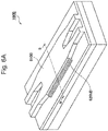
Fig. 6A is a perspective view of a 2x2 MMI optical multiplexer/demultiplexer 100B according to a second example embodiment. -
Fig. 6B is a sectional view of a 2x2 MMI optical multiplexer/demultiplexer 100B according to a second example embodiment, which is taken along line B-B'. -
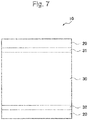
Fig. 7 is a top view of a rib typeoptical waveguide 10. - A first example embodiment according to the present invention will be described. The present example embodiment employs a 2x2 MMI optical multiplexer/demultiplexer based on a semiconductor rib-type optical waveguide. A perspective view of the 2x2 MMI optical multiplexer/demultiplexer according to present example embodiment is illustrated in
Fig. 1A and its sectional view taken along line A-A' ofFig. 1A is illustrated inFig. 1B . InFig. 1A andFig. 1B , a 2x2 MMI optical multiplexer/demultiplexer 100 includes a SOI substrate (SOI: Semiconductor-on-Insulator) 200, inputoptical waveguides optical waveguides optical waveguides type MMI region 600. The inputoptical waveguides optical waveguides optical waveguides - The
SOI substrate 200 is a semiconductor slab region and is formed by arranging an insulatingfilm 220 on an upper surface of asubstrate 210 and arranging aSOI layer 230 on the surface of the insulatingfilm 220. Then, optical waveguide patterns are exposed to theSOI layer 230 with high precision and a dry etching process is performed, so that the input optical waveguide 300, the output optical waveguide 400, the tapered optical waveguide 500, and the ribtype MMI region 600 are formed. - The input
optical waveguides SOI layer 230 of theSOI substrate 200, and form single mode optical waveguides of a pair of input sides. Optical signals inputted to the inputoptical waveguides type MMI region 600 via the continuous taperedoptical waveguides - The output
optical waveguides SOI layer 230 of theSOI substrate 200, and form single mode optical waveguides of a pair of output sides. The outputoptical waveguides type MMI region 600 via the continuous taperedoptical waveguides optical waveguides optical waveguides - The tapered optical waveguide 500 smoothly connects the input optical waveguide 300 or the output optical waveguide 400 to the rib
type MMI region 600. In the present example embodiment, all the four taperedoptical waveguides Fig. 1A , the taperedoptical waveguide 500a smoothly connects the inputoptical waveguide 300a to aMMI part 610 of the ribtype MMI region 600, and the taperedoptical waveguide 500b smoothly connects the inputoptical waveguide 300b to theMMI part 610. Furthermore, the taperedoptical waveguide 500c smoothly connects the outputoptical waveguide 400a to theMMI part 610 of the ribtype MMI region 600, and the taperedoptical waveguide 500d smoothly connects the outputoptical waveguide 400b to theMMI part 610. - The rib
type MMI region 600 includes a semiconductor and allows an optical signal inputted from the inputoptical waveguide 300a via the taperedoptical waveguides 500a to interfere with an optical signal inputted from the inputoptical waveguide 300b via the taperedoptical waveguides 500b. Then, the ribtype MMI region 600 outputs the interfered optical signal to the outputoptical waveguides optical waveguides type MMI region 600 according to the present example embodiment, thin stepped parts with a finite width are formed at both sidewalls extending in a direction (hereinafter, written as a longitudinal direction) toward the output optical waveguide 400 from the input optical waveguide 300. Hereinafter, the stepped parts are written as narrow width steppedparts parts MMI part 610. Widths w of the steppedparts parts Fig. 1B . -
Fig. 2A andFig. 2B illustrate a difference n11-n12 (hereinafter, an effective refractive index difference) of a unique value (an effective refractive index n11) of a basic mode and a unique value (an effective refractive index n12) of a first high order mode of the ribtype MMI region 600 when the sectional shapes of the narrow width steppedparts demultiplexer 100 configured as above. The effective refractive index difference is inversely proportional to an interference cycle (a beat length) of the basic mode and the first high order mode in the ribtype MMI region 600, and is an important parameter for deciding an optimal length of the ribtype MMI region 600. InFig. 2A andFig. 2B , a subscript of the effective refractive index difference n is written using a sign E of an electric field, but has the same meaning as that of the notation in the present specification. -
Fig. 2A illustrates an effective refractive index difference (nx 11-nx 12) when a main electric field is horizontal to a substrate (an Ex mode), andFig. 2B illustrates an effective refractive index difference (ny 11-ny 12) when the main electric field is vertical to the substrate (an Ey mode). InFig. 2A andFig. 2B , it is assumed that a horizontal axis denotes widths w of the narrow width steppedparts parts parts MMI part 610 is 7 µm, a rib height is 0.9 µm, and a slab thickness is 0.6 µm. - In
Fig. 2A andFig. 2B , an absolute value of the effective refractive index difference is about an amount of 5×10⁻³ in the Ex mode and the Ey mode and corresponds to more than 200 µm when it is converted to an MMI optimal length for signal light with a wavelength of 1,550 nm. - In a general semiconductor rib type optical waveguide-based MMI optical multiplexer/demultiplexer, the narrow width stepped
parts MMI part 610. This state corresponds to the lower left origins (the width w and the height h are all zero) ofFig. 2A andFig. 2B . When the effective refractive index difference is constant (that is, a beat length is constant), the widths w and the heights h of the narrow width steppedparts Fig. 2A andFig. 2B . This tendency is common to both the Ex mode and the Ey mode, but the absolute value itself of the effective refractive index difference slightly deviates between both modes. - In order to instinctively indicate deviation in polarization of the absolute values of the effective refractive index difference, in other words, deviation in optimal lengths of both polarization in the rib
type MMI region 600,Fig. 3 illustrates a ratio (nx 11-nx 12)/(ny 11-ny 12) of the effective refractive index differences of the Ex mode and the Ey mode. - In
Fig. 3 , the ratio of polarization of the effective refractive index differences monotonically decreases as the widths w and the heights h of the narrow width steppedparts type MMI region 600 coincide with each other, that is, when it is assumed that there is no influence of the input/output optical waveguide, it is probable that it is possible to perform a polarization independent operation of the 2x2 MMI optical multiplexer/demultiplexer. - While the ratio of the effective refractive index differences is about 1.025 in the vicinity of the lower left origin of
Fig. 3 , the ratio is 1 when the height h is about 0.5 µm and the width w is about 1 µm. This means that it is possible to adjust the polarization dependence of the 2x2 MMI optical multiplexer/demultiplexer 100 within a certain range by adjusting the widths w and the heights h of the narrow width steppedparts MMI part 610. That is, when beat lengths in theMMI part 610 coincide with each other between both polarization, if only the ribtype MMI region 600 is considered, it is possible to design the narrow width steppedparts parts - In addition, the aforementioned discussion corresponds to the case of focusing on only the effective refractive index difference (the beat length) in the rib
type MMI region 600 in which the narrow width steppedparts type MMI region 600 can be excited with an ideal planar wave. However, it is general that a reversible tapered optical waveguide region is arranged between the ribtype MMI region 600, and the input optical waveguide 300 and the output optical waveguide 400. By so doing, the two-dimensional electromagnetic field distribution of two optical waveguides connected to both ends of input and output continuously changes. As signal light propagates the reversible tapered optical waveguide region, a beam shape (mainly, a beam width) continuously changes (the beam with is mainly extended or reduced), and simultaneously an equiphase surface (a wave front) is distorted from a plane (a curvature changes). In addition, when the reversible tapered optical waveguide region is formed with the taperedoptical waveguides SOI layer 230 in a strip shape, the reversible tapered optical waveguide region itself has polarization dependence. - The curvature of the equiphase surface (the wave front) is considered as an amount proportional to a propagation distance, and when the lengths of the tapered
optical waveguides optical waveguides optical waveguides type MMI region 600, signal light is not excited with a plane wave, but is excited in the state in which the equiphase surface (the wave front) has been distorted. This causes finite loss and polarization dependence is shown in the loss itself. - From the above, the extent of contribution of polarization dependence shown by the tapered
optical waveguides demultiplexer 100. The case in which, the inter-polarization ratio (nx 11-nx 12)/(ny 11-ny 12) of the absolute values of the effective refractive index differences in the ribtype MMI region 600 is about 1.02, is equivalent to the case of a sectional shape in which the effective refractive index difference of the Ex mode is larger than the effective refractive index difference of the Ey mode by about 2%. In this case, the fact that the 2x2 MMI optical multiplexer/demultiplexer 100 including the taperedoptical waveguides type MMI region 600 performs a polarization independent operation is separately confirmed through electromagnetic field analysis. - In addition, as illustrated in
Fig. 3 , in the effective refractive index difference of the ribtype MMI region 600, the heights h and the widths w of the narrow width steppedparts parts parts parts parts - Furthermore, if the polarization dependence is decided only by the sectional areas of the narrow width stepped
parts parts type MMI region 600, particularly, selection methods of etching conditions, there is a case in which a rib sidewall is inclined from a surface vertical to the substrate. However, when an inclination is allowed to occur in the rib sidewall of the ribtype MMI region 600, the rib sidewalls of the input optical waveguide 300, the output optical waveguide 400, and the tapered optical waveguide 500 are also inclined. In this case, the electromagnetic field distributions of the basic modes of the input optical waveguide 300 and the output optical waveguide 400 deviate from an assumed shape, so that design of polarization independence becomes difficult. Accordingly, it is practical that the sectional shapes of the narrow width steppedparts - The operation of the 2x2 MMI optical multiplexer/
demultiplexer 100 described in the first example embodiment will be described. The insulatingfilm 220 including a SiO2 film with a thickness of 3 µm and theSOI layer 230 serving as a semiconductor layer with a thickness of 1.5 µm are arranged on thesubstrate 210, so that theSOI substrate 200 is formed. Moreover, optical waveguide patterns are high precisely formed in theSOI layer 230 on theSOI substrate 200 by using a photolithography technology, so that the 2x2 MMI optical multiplexer/demultiplexer 100 described in the first example embodiment is formed. - The input optical waveguide 300 and the output optical waveguide 400 are rib type optical waveguides in which Si is used as a core and SiO2 is used as a clad, and have a rib width of 1.4 µm, a rib height of 0.9 µm, and a slab thickness of 0.6 µm. Furthermore, in a wavelength band of 1,530 nm to 1,610 nm, the input optical waveguide 300 and the output optical waveguide 400 satisfy single mode propagation conditions together with both polarization of the Ex mode and the Ey mode. The
MMI part 610 of the ribtype MMI region 600 is formed to have a width of 7 µm, a length of 234 µm, a rib height of 0.9 µm, and a slab thickness of 0.6 µm. Furthermore, the narrow width steppedparts type MMI region 600 are smoothly connected to each other by the tapered optical waveguide 500 (a reversible horizontal tapered region) having a length of 50 µm in which a rib height is 0.9 µm, a slab thickness is 0.6 µm, and a width is linearly changed from 1.4 µm to 3 µm. - These are highly precisely processed with precision of ± 20 nm or less together with a width and a thickness by applying the most advanced CMOS process such as high precision photolithography using a reduction projection exposure device using ArF in a light source and a phase shift mask, and a low damage dry etching technology. Furthermore, in a process in the vicinity of the rib
type MMI region 600, a previously stepped SiN film (not illustrated because it is removed in a manufacturing process) is provided as an etching blocking layer to be provided to the surface of theSOI substrate 200, so that theMMI part 610 and the narrow width steppedparts - The transmittance for the Ex mode of the 2x2 MMI optical multiplexer/
demultiplexer 100 formed as described above is illustrated inFig. 4 , and a ratio (that is, polarization dependence of transmittance) of the transmittance for the Ex mode and the transmittance for the Ey mode is illustrated inFig. 5 . InFig. 4 andFig. 5 , a horizontal axis denotes the width of a tapered end portion (a wide side being in contact with the MMI part 610) of the tapered optical waveguide 500, and a vertical axis denotes the length of the ribtype MMI region 600. A signal light wavelength is 1,590 nm. The transmittance is defined byEquation 1 below.
- In
Equation 1 above, Pbar denotes power outputted to a port (a bar output port) of the output optical waveguide 400 in front of signal light with power Pin travelling straight from one side of the input optical waveguide 300, and Pcross denotes power outputted to a port (a cross output port) of the output optical waveguide 400 in front of a diagonal line of theMMI part 610. - As apparent from
Fig. 4 , the width and the MMI length dependence of a tapered end portion of insertion loss for the Ex mode form a track-like contour line group in which a size differs step by step. The maximum value (the minimum value of the insertion loss) of the transmittance is -0.04 dB to -0.06 dB (+0.04 dB to +0.06 dB), so that a favorable value can be obtained for a 2x2 optical multiplexer/demultiplexer for a 1.5 µm band using Si as an optical waveguide core material. - A white line of
Fig. 5 indicates that the transmittance ratio of the Ex mode and the Ey mode is 1 (=0 dB), that is, indicates a polarization independence condition. From this, in the case of designing a practical 2x2 MMI optical multiplexer/demultiplexer with maximum transmittance (insertion loss is minimum) and polarization independence, it is sufficient if there is a condition (the width of the tapered end portion and the length of the MMI part) in which a transmittance maximum region inFig. 4 overlaps the white line inFig. 5 with each other. Specifically, for example, it is sufficient if the length of theMMI part 610 is 232 µm and the width of the tapered end portion of the tapered optical waveguide 500 is 3.3 µm. - Similarly to the case in which a signal light wavelength is 1,590 nm, in the case in which a signal light wavelength is from 1,570 nm to 1,610 nm, the transmittance for the Ex mode, as well as a ratio of the transmittance for the Ex mode and the transmittance for the Ey mode is calculated (not illustrated). From the result, the length of the
MMI part 610 of the 2x2 MMI optical multiplexer/demultiplexer 100 is set to 232 µm and the width of the tapered end portion is set to 3.3 µm. - The 2x2 MMI optical multiplexer/
demultiplexer 100 designed as described above has practical signal light branching characteristics in the signal light wavelength from 1,570 nm to 1,610 nm in configuring a matrix optical switch even though it is a rib type optical waveguide using the Si core whose section is not a square. Specifically, in relation to the insertion loss, the Ex mode is from 0.08 dB to 0.09 dB, the Ey mode is from 0.07 dB to 0.08 dB, and polarization dependence loss is ±0.01 dB or less. - As described above, according to the present example embodiment, in the 2x2 MMI optical multiplexer/
demultiplexer 100 including the input/output tapered waveguides, it can be understood that it is possible to achieve a structure, in which polarization dependence and wavelength dependence in multiplexing and demultiplexing characteristics are suppressed to a level causing practically no problems over a wide wavelength band, by a practical means by adding required minimum steps. - In addition, the rib
type MMI region 600, in which the narrow width steppedparts MMI part 610, can be arranged in a ROADM (reconfigurable optical add/drop multiplexer), a 90 ° hybrid, an ADM matrix switch and the like, in addition to the MMI optical multiplexer/demultiplexer. - A second example embodiment will be described. A perspective view of a 2x2 MMI optical multiplexer/
demultiplexer 100B according to the present example embodiment is illustrated inFig. 6A , and its sectional view taken along line B-B' is illustrated inFig. 6B . In the present example embodiment, narrow width stepped parts 620aB and 620bB are formed in a stair shape by notching corner parts in a rectangular parallelepiped shape while maintaining the areas of the rectangular parallelepiped narrow width steppedparts - Specifically, in each of the narrow width stepped parts 620aB and 620bB according to the present example embodiment, a lower part having a width of 0.4 µm and a height of 0.2 µm and an upper part having a width of 0.2 µm and a height of 0.2 µm are integrally formed with each other. Except for this point, the narrow width stepped parts 620aB and 620bB are similar to those of the 2x2 MMI optical multiplexer/
demultiplexer 100 described in the example of the first example embodiment. In addition, in a manufacturing method thereof, for the lithography process of the narrow width stepped parts 620aB and 620bB, one mask and a one-time dry etching process of an etching barrier layer are respectively added to the case of the aforementioned example. - Similarly to the 2x2 MMI optical multiplexer/
demultiplexer 100 ofFig. 1 described in the example of the first example embodiment, the 2x2 MMI optical multiplexer/demultiplexer 100B ofFig. 6A andFig. 6B also obtains practical signal light branching characteristics as a 2x2 optical multiplexer/demultiplexer used in configuring a matrix optical switch even though it is a rib type optical waveguide in which its section is not a square and a Si core is used. Specifically, in relation to loss, the Ex mode is from 0.08 dB to 0.09 dB, the Ey mode is from 0.07 dB to 0.08 dB, and polarization dependence loss is ±0.01 dB or less over the signal light wavelength from 1,570 nm to 1,610 nm. - In the aforementioned entire example embodiment, Si is used as a core material; however, it is possible to expect similar effects even in the case of using dielectric substances other than Si as a core. Furthermore, since it is not proper to use the
SOI substrate 200 in the case of compound semiconductors and the like, optical confinement in a lamination direction (a direction vertical to a substrate) is reduced. However, also in this case, since a design concept is applicable, it is sufficient if a process of applying a proper perturbation to a sectional shape is performed in order to suppress polarization dependence of an effective refractive index difference at both sides of the MMI region. Moreover, the number of each of the input/output optical waveguides is not limited to 2, and the input/output optical waveguides can be applied to a M input N output (M×N) MMI optical multiplexer/demultiplexer. - In addition, the rib type optical waveguide according to the aforementioned example embodiment can be formed by the minimum constituent members illustrated in
Fig. 7 . That is, a rib typeoptical waveguide 10 can be formed by asubstrate 20 and a multi-modeoptical interference region 30 formed on the upper surface of thesubstrate 20 and including a rib type optical waveguide. It is characteristic that both side surfaces of the multi-modeoptical interference region 30 are respectively formed in steppedshapes - The present invention is not limited to the aforementioned example embodiments and design changes and the like in the range of not departing from the scope of the present invention are also included in the present invention.
- The present invention can be applied to all waveguide optical switches which are used in a MxN matrix optical switch and the like and include input/output optical waveguides and multi-mode interference regions formed on the same substrate.
- This application is based upon and claims the benefit of priority from Japanese patent application No.
2014-204120, filed on October 2, 2014 -
- 10
- Rib type optical waveguide
- 20
- Substrate
- 30
- Multi-mode optical interference region
- 100
- 2×2 MMI optical multiplexer/demultiplexer
- 200
- SOI substrate
- 210
- Substrate
- 220
- Insulating film
- 230
- SOI layer
- 300a, 300b
- Input optical waveguide
- 400a, 400b
- Output optical waveguide
- 500a, 500b, 500c, 500d
- Tapered optical waveguide
- 600
- Rib type MMI region
- 610
- MMI part
- 620a, 620b
- Narrow width stepped part
Claims (10)
- A rib type optical waveguide, comprising:a substrate; anda multi-mode optical interference region including a rib type optical waveguide formed on an upper surface of the substrate,wherein each of both side surfaces of the multi-mode optical interference region are formed in a stepped shape.
- The rib type optical waveguide according to Claim 1, wherein a width of a stepped part is equal to or less than a propagation wavelength and a height of the stepped part is equal to or less than a half of the propagation wavelength.
- The rib type optical waveguide according to Claim 1 or 2, wherein, on the upper surface of the substrate, an insulating film and a semiconductor layer are arranged, and a core of the rib type optical waveguide is formed by processing the semiconductor layer in a strip shape.
- The rib type optical waveguide according to any one of Claims 1 to 3, wherein the stepped part is formed in a stair shape of two stages or more.
- An optical multiplexer/demultiplexer, comprising:M input optical waveguides and N output optical waveguides including a single mode rib type optical waveguide;reversible tapered regions that smoothly connect the input optical waveguides and the output optical waveguides to multi-mode optical interference regions and include MxN rib type optical waveguides; andthe rib type optical waveguide according to any one of Claims 1 to 4,wherein the input optical waveguides, the output optical waveguides, the multi-mode optical interference regions, and the reversible tapered regions are formed on a substrate.
- The optical multiplexer/demultiplexer according to Claim 5, wherein, on an upper surface of the substrate, an insulating film and a semiconductor layer are arranged, and cores of the input optical waveguides, the output optical waveguides, the multi-mode optical interference regions, and the reversible tapered regions are formed by processing the semiconductor layer in a strip shape.
- The optical multiplexer/demultiplexer according to Claim 5 or 6, wherein the input optical waveguides and the output optical waveguides include a same sectional shape.
- The optical multiplexer/demultiplexer according to any one of Claims 5 to 7, wherein all the MxN reversible tapered regions include same length and same tapered width.
- The optical multiplexer/demultiplexer according to Claim 8, wherein the length of the reversible tapered region is longer than a propagation wavelength.
- The optical multiplexer/demultiplexer according to any one of Claims 5 to 9, wherein two input optical waveguides, two output optical waveguides, and four reversible tapered regions are provided.
Applications Claiming Priority (2)
| Application Number | Priority Date | Filing Date | Title |
|---|---|---|---|
| JP2014204120 | 2014-10-02 | ||
| PCT/JP2015/004689 WO2016051698A1 (en) | 2014-10-02 | 2015-09-15 | Rib type optical waveguide and optical multiplexer/demultiplexer using same |
Publications (3)
| Publication Number | Publication Date |
|---|---|
| EP3203282A1 true EP3203282A1 (en) | 2017-08-09 |
| EP3203282A4 EP3203282A4 (en) | 2018-06-06 |
| EP3203282B1 EP3203282B1 (en) | 2022-01-26 |
Family
ID=55629775
Family Applications (1)
| Application Number | Title | Priority Date | Filing Date |
|---|---|---|---|
| EP15846939.5A Active EP3203282B1 (en) | 2014-10-02 | 2015-09-15 | Rib type optical waveguide and optical multiplexer/demultiplexer using same |
Country Status (4)
| Country | Link |
|---|---|
| US (1) | US10082623B2 (en) |
| EP (1) | EP3203282B1 (en) |
| JP (1) | JP6798313B2 (en) |
| WO (1) | WO2016051698A1 (en) |
Families Citing this family (6)
| Publication number | Priority date | Publication date | Assignee | Title |
|---|---|---|---|---|
| JP7480488B2 (en) | 2019-10-04 | 2024-05-10 | 富士通オプティカルコンポーネンツ株式会社 | Optical semiconductor device and receiver |
| US10862610B1 (en) | 2019-11-11 | 2020-12-08 | X Development Llc | Multi-channel integrated photonic wavelength demultiplexer |
| US11187854B2 (en) * | 2019-11-15 | 2021-11-30 | X Development Llc | Two-channel integrated photonic wavelength demultiplexer |
| JP7460931B2 (en) * | 2020-07-31 | 2024-04-03 | 日本電信電話株式会社 | Planar optical waveguide device |
| US11360268B1 (en) | 2021-03-17 | 2022-06-14 | Cisco Technology, Inc. | Low-loss and low-crosstalk optical mode multiplexer and optical crossover |
| CN118584585B (en) * | 2024-06-28 | 2026-04-24 | 吉林大学 | Optical mode demultiplexer based on cascaded silica multimode interferometer structure |
Family Cites Families (14)
| Publication number | Priority date | Publication date | Assignee | Title |
|---|---|---|---|---|
| GB1525492A (en) * | 1974-09-20 | 1978-09-20 | Max Planck Gesellschaft | Self imaging system using a waveguide |
| JPH04247408A (en) | 1991-02-01 | 1992-09-03 | Ibiden Co Ltd | Optical waveguide |
| CA2331981A1 (en) | 1998-05-08 | 1999-11-18 | Richard M. Osgood, Jr. | Reduced size multimode interference based coupler |
| JP2001183710A (en) | 1999-12-27 | 2001-07-06 | Kddi Corp | Multimode interference waveguide type optical switch |
| US6856732B2 (en) * | 2001-06-13 | 2005-02-15 | Intel Corporation | Method and apparatus for adding/droping optical signals in a semiconductor substrate |
| FI20020698A0 (en) * | 2002-04-11 | 2002-04-11 | Valtion Teknillinen | Integrated optical circuit optical channel and method for producing a optical channel |
| SE528653C2 (en) * | 2005-05-30 | 2007-01-09 | Phoxtal Comm Ab | Integrated chip |
| US7116880B1 (en) | 2005-06-30 | 2006-10-03 | Xerox Corporation | Decreased crosstalk in adjacent photonic waveguides |
| US7184207B1 (en) * | 2005-09-27 | 2007-02-27 | Bookham Technology Plc | Semiconductor optical device |
| GB2438222A (en) * | 2006-05-17 | 2007-11-21 | Bookham Technology Plc | Multimode interference waveguide coupler |
| JP5120330B2 (en) | 2009-04-27 | 2013-01-16 | 三菱電機株式会社 | Semiconductor optical device and manufacturing method thereof |
| WO2011019887A2 (en) * | 2009-08-14 | 2011-02-17 | Massachusetts Institute Of Technology | Waveguide coupler having continuous three-dimensional tapering |
| JP5413865B1 (en) * | 2012-12-27 | 2014-02-12 | 株式会社フジクラ | Optical waveguide device and optical modulator |
| CN204302526U (en) * | 2014-12-26 | 2015-04-29 | 江苏尚飞光电科技有限公司 | Polarization beam splitting circulator |
-
2015
- 2015-09-15 JP JP2016551505A patent/JP6798313B2/en active Active
- 2015-09-15 WO PCT/JP2015/004689 patent/WO2016051698A1/en not_active Ceased
- 2015-09-15 US US15/514,563 patent/US10082623B2/en active Active
- 2015-09-15 EP EP15846939.5A patent/EP3203282B1/en active Active
Also Published As
| Publication number | Publication date |
|---|---|
| EP3203282A4 (en) | 2018-06-06 |
| JPWO2016051698A1 (en) | 2017-07-13 |
| WO2016051698A1 (en) | 2016-04-07 |
| EP3203282B1 (en) | 2022-01-26 |
| JP6798313B2 (en) | 2020-12-09 |
| US10082623B2 (en) | 2018-09-25 |
| US20170227712A1 (en) | 2017-08-10 |
Similar Documents
| Publication | Publication Date | Title |
|---|---|---|
| EP3203282B1 (en) | Rib type optical waveguide and optical multiplexer/demultiplexer using same | |
| EP3111263B1 (en) | Apparatus and method for waveguide polarizer comprizing series of bends | |
| EP1226461B1 (en) | Phasar with flattened pass-band | |
| US6873777B2 (en) | Two-dimensional photonic crystal device | |
| JP4448199B2 (en) | Substrate-type optical waveguide device, chromatic dispersion compensation device, optical filter and optical resonator, and design methods thereof | |
| US20020159703A1 (en) | Optical apparatus and method having predetermined group velocity dispersion | |
| EP2378329B1 (en) | Optical wavelength multiplexing/demultiplexing circuit, optical module using optical wavelength multiplexing/demultiplexing circuit, and communication system | |
| JP4208754B2 (en) | Optical delay element | |
| CN110573918B (en) | T-shaped arrayed waveguide grating | |
| JP5263045B2 (en) | Polarization-independent optical device | |
| US10746932B2 (en) | Multi-mode interference coupler | |
| JPWO2009107798A1 (en) | Optical waveguide device, chromatic dispersion compensation device and design method thereof, optical filter and design method thereof, and optical resonator and design method thereof | |
| CN104603654A (en) | Optical waveguide element | |
| JP2007072433A (en) | Optical integrated device and optical control device | |
| CN107407776B (en) | High Refractive Index Contrast Photonic Devices and Their Applications | |
| JP2014041252A (en) | Optical waveguide element | |
| CN112601994A (en) | Photonic device for splitting light beam | |
| WO2014030576A1 (en) | Optical waveguide element | |
| US20040228574A1 (en) | Switchable optical dispersion compensator using Bragg-grating | |
| WO2018022296A1 (en) | Reconfigurable athermal optical filters | |
| Truong et al. | A design of triplexer based on a 2× 2 butterfly MMI coupler and a directional coupler using silicon waveguides | |
| JP2013041146A (en) | Wavelength-selective multimode interference waveguide device | |
| Juhari et al. | Optical loss analysis in 13-channel SOI-based AWG for CWDM network | |
| JP5504476B2 (en) | Optical waveguide crossing structure | |
| JP2011043665A (en) | Wavelength multiplexer/demultiplexer |
Legal Events
| Date | Code | Title | Description |
|---|---|---|---|
| STAA | Information on the status of an ep patent application or granted ep patent |
Free format text: STATUS: THE INTERNATIONAL PUBLICATION HAS BEEN MADE |
|
| PUAI | Public reference made under article 153(3) epc to a published international application that has entered the european phase |
Free format text: ORIGINAL CODE: 0009012 |
|
| STAA | Information on the status of an ep patent application or granted ep patent |
Free format text: STATUS: REQUEST FOR EXAMINATION WAS MADE |
|
| 17P | Request for examination filed |
Effective date: 20170502 |
|
| AK | Designated contracting states |
Kind code of ref document: A1 Designated state(s): AL AT BE BG CH CY CZ DE DK EE ES FI FR GB GR HR HU IE IS IT LI LT LU LV MC MK MT NL NO PL PT RO RS SE SI SK SM TR |
|
| AX | Request for extension of the european patent |
Extension state: BA ME |
|
| DAV | Request for validation of the european patent (deleted) | ||
| DAX | Request for extension of the european patent (deleted) | ||
| A4 | Supplementary search report drawn up and despatched |
Effective date: 20180507 |
|
| RIC1 | Information provided on ipc code assigned before grant |
Ipc: G02B 6/125 20060101ALI20180430BHEP Ipc: G02B 6/293 20060101ALI20180430BHEP Ipc: G02B 6/28 20060101ALI20180430BHEP Ipc: G02B 6/12 20060101ALN20180430BHEP Ipc: G02B 6/122 20060101AFI20180430BHEP |
|
| STAA | Information on the status of an ep patent application or granted ep patent |
Free format text: STATUS: EXAMINATION IS IN PROGRESS |
|
| 17Q | First examination report despatched |
Effective date: 20200220 |
|
| RIC1 | Information provided on ipc code assigned before grant |
Ipc: G02B 6/12 20060101ALN20210604BHEP Ipc: G02B 6/293 20060101ALI20210604BHEP Ipc: G02B 6/28 20060101ALI20210604BHEP Ipc: G02B 6/125 20060101ALI20210604BHEP Ipc: G02B 6/122 20060101AFI20210604BHEP |
|
| RIC1 | Information provided on ipc code assigned before grant |
Ipc: G02B 6/12 20060101ALN20210611BHEP Ipc: G02B 6/293 20060101ALI20210611BHEP Ipc: G02B 6/28 20060101ALI20210611BHEP Ipc: G02B 6/125 20060101ALI20210611BHEP Ipc: G02B 6/122 20060101AFI20210611BHEP |
|
| RIC1 | Information provided on ipc code assigned before grant |
Ipc: G02B 6/12 20060101ALN20210721BHEP Ipc: G02B 6/293 20060101ALI20210721BHEP Ipc: G02B 6/28 20060101ALI20210721BHEP Ipc: G02B 6/125 20060101ALI20210721BHEP Ipc: G02B 6/122 20060101AFI20210721BHEP |
|
| GRAP | Despatch of communication of intention to grant a patent |
Free format text: ORIGINAL CODE: EPIDOSNIGR1 |
|
| STAA | Information on the status of an ep patent application or granted ep patent |
Free format text: STATUS: GRANT OF PATENT IS INTENDED |
|
| RIC1 | Information provided on ipc code assigned before grant |
Ipc: G02B 6/12 20060101ALN20210820BHEP Ipc: G02B 6/293 20060101ALI20210820BHEP Ipc: G02B 6/28 20060101ALI20210820BHEP Ipc: G02B 6/125 20060101ALI20210820BHEP Ipc: G02B 6/122 20060101AFI20210820BHEP |
|
| INTG | Intention to grant announced |
Effective date: 20210915 |
|
| GRAS | Grant fee paid |
Free format text: ORIGINAL CODE: EPIDOSNIGR3 |
|
| GRAA | (expected) grant |
Free format text: ORIGINAL CODE: 0009210 |
|
| STAA | Information on the status of an ep patent application or granted ep patent |
Free format text: STATUS: THE PATENT HAS BEEN GRANTED |
|
| AK | Designated contracting states |
Kind code of ref document: B1 Designated state(s): AL AT BE BG CH CY CZ DE DK EE ES FI FR GB GR HR HU IE IS IT LI LT LU LV MC MK MT NL NO PL PT RO RS SE SI SK SM TR |
|
| REG | Reference to a national code |
Ref country code: GB Ref legal event code: FG4D |
|
| REG | Reference to a national code |
Ref country code: CH Ref legal event code: EP |
|
| REG | Reference to a national code |
Ref country code: AT Ref legal event code: REF Ref document number: 1465723 Country of ref document: AT Kind code of ref document: T Effective date: 20220215 |
|
| REG | Reference to a national code |
Ref country code: IE Ref legal event code: FG4D |
|
| REG | Reference to a national code |
Ref country code: DE Ref legal event code: R096 Ref document number: 602015076709 Country of ref document: DE |
|
| REG | Reference to a national code |
Ref country code: LT Ref legal event code: MG9D |
|
| REG | Reference to a national code |
Ref country code: NL Ref legal event code: MP Effective date: 20220126 |
|
| REG | Reference to a national code |
Ref country code: AT Ref legal event code: MK05 Ref document number: 1465723 Country of ref document: AT Kind code of ref document: T Effective date: 20220126 |
|
| PG25 | Lapsed in a contracting state [announced via postgrant information from national office to epo] |
Ref country code: NL Free format text: LAPSE BECAUSE OF FAILURE TO SUBMIT A TRANSLATION OF THE DESCRIPTION OR TO PAY THE FEE WITHIN THE PRESCRIBED TIME-LIMIT Effective date: 20220126 |
|
| PG25 | Lapsed in a contracting state [announced via postgrant information from national office to epo] |
Ref country code: SE Free format text: LAPSE BECAUSE OF FAILURE TO SUBMIT A TRANSLATION OF THE DESCRIPTION OR TO PAY THE FEE WITHIN THE PRESCRIBED TIME-LIMIT Effective date: 20220126 Ref country code: RS Free format text: LAPSE BECAUSE OF FAILURE TO SUBMIT A TRANSLATION OF THE DESCRIPTION OR TO PAY THE FEE WITHIN THE PRESCRIBED TIME-LIMIT Effective date: 20220126 Ref country code: PT Free format text: LAPSE BECAUSE OF FAILURE TO SUBMIT A TRANSLATION OF THE DESCRIPTION OR TO PAY THE FEE WITHIN THE PRESCRIBED TIME-LIMIT Effective date: 20220526 Ref country code: NO Free format text: LAPSE BECAUSE OF FAILURE TO SUBMIT A TRANSLATION OF THE DESCRIPTION OR TO PAY THE FEE WITHIN THE PRESCRIBED TIME-LIMIT Effective date: 20220426 Ref country code: LT Free format text: LAPSE BECAUSE OF FAILURE TO SUBMIT A TRANSLATION OF THE DESCRIPTION OR TO PAY THE FEE WITHIN THE PRESCRIBED TIME-LIMIT Effective date: 20220126 Ref country code: HR Free format text: LAPSE BECAUSE OF FAILURE TO SUBMIT A TRANSLATION OF THE DESCRIPTION OR TO PAY THE FEE WITHIN THE PRESCRIBED TIME-LIMIT Effective date: 20220126 Ref country code: ES Free format text: LAPSE BECAUSE OF FAILURE TO SUBMIT A TRANSLATION OF THE DESCRIPTION OR TO PAY THE FEE WITHIN THE PRESCRIBED TIME-LIMIT Effective date: 20220126 Ref country code: BG Free format text: LAPSE BECAUSE OF FAILURE TO SUBMIT A TRANSLATION OF THE DESCRIPTION OR TO PAY THE FEE WITHIN THE PRESCRIBED TIME-LIMIT Effective date: 20220426 |
|
| PG25 | Lapsed in a contracting state [announced via postgrant information from national office to epo] |
Ref country code: PL Free format text: LAPSE BECAUSE OF FAILURE TO SUBMIT A TRANSLATION OF THE DESCRIPTION OR TO PAY THE FEE WITHIN THE PRESCRIBED TIME-LIMIT Effective date: 20220126 Ref country code: LV Free format text: LAPSE BECAUSE OF FAILURE TO SUBMIT A TRANSLATION OF THE DESCRIPTION OR TO PAY THE FEE WITHIN THE PRESCRIBED TIME-LIMIT Effective date: 20220126 Ref country code: GR Free format text: LAPSE BECAUSE OF FAILURE TO SUBMIT A TRANSLATION OF THE DESCRIPTION OR TO PAY THE FEE WITHIN THE PRESCRIBED TIME-LIMIT Effective date: 20220427 Ref country code: FI Free format text: LAPSE BECAUSE OF FAILURE TO SUBMIT A TRANSLATION OF THE DESCRIPTION OR TO PAY THE FEE WITHIN THE PRESCRIBED TIME-LIMIT Effective date: 20220126 Ref country code: AT Free format text: LAPSE BECAUSE OF FAILURE TO SUBMIT A TRANSLATION OF THE DESCRIPTION OR TO PAY THE FEE WITHIN THE PRESCRIBED TIME-LIMIT Effective date: 20220126 |
|
| PG25 | Lapsed in a contracting state [announced via postgrant information from national office to epo] |
Ref country code: IS Free format text: LAPSE BECAUSE OF FAILURE TO SUBMIT A TRANSLATION OF THE DESCRIPTION OR TO PAY THE FEE WITHIN THE PRESCRIBED TIME-LIMIT Effective date: 20220526 |
|
| REG | Reference to a national code |
Ref country code: DE Ref legal event code: R097 Ref document number: 602015076709 Country of ref document: DE |
|
| PG25 | Lapsed in a contracting state [announced via postgrant information from national office to epo] |
Ref country code: SM Free format text: LAPSE BECAUSE OF FAILURE TO SUBMIT A TRANSLATION OF THE DESCRIPTION OR TO PAY THE FEE WITHIN THE PRESCRIBED TIME-LIMIT Effective date: 20220126 Ref country code: SK Free format text: LAPSE BECAUSE OF FAILURE TO SUBMIT A TRANSLATION OF THE DESCRIPTION OR TO PAY THE FEE WITHIN THE PRESCRIBED TIME-LIMIT Effective date: 20220126 Ref country code: RO Free format text: LAPSE BECAUSE OF FAILURE TO SUBMIT A TRANSLATION OF THE DESCRIPTION OR TO PAY THE FEE WITHIN THE PRESCRIBED TIME-LIMIT Effective date: 20220126 Ref country code: EE Free format text: LAPSE BECAUSE OF FAILURE TO SUBMIT A TRANSLATION OF THE DESCRIPTION OR TO PAY THE FEE WITHIN THE PRESCRIBED TIME-LIMIT Effective date: 20220126 Ref country code: DK Free format text: LAPSE BECAUSE OF FAILURE TO SUBMIT A TRANSLATION OF THE DESCRIPTION OR TO PAY THE FEE WITHIN THE PRESCRIBED TIME-LIMIT Effective date: 20220126 Ref country code: CZ Free format text: LAPSE BECAUSE OF FAILURE TO SUBMIT A TRANSLATION OF THE DESCRIPTION OR TO PAY THE FEE WITHIN THE PRESCRIBED TIME-LIMIT Effective date: 20220126 |
|
| PG25 | Lapsed in a contracting state [announced via postgrant information from national office to epo] |
Ref country code: AL Free format text: LAPSE BECAUSE OF FAILURE TO SUBMIT A TRANSLATION OF THE DESCRIPTION OR TO PAY THE FEE WITHIN THE PRESCRIBED TIME-LIMIT Effective date: 20220126 |
|
| PLBE | No opposition filed within time limit |
Free format text: ORIGINAL CODE: 0009261 |
|
| STAA | Information on the status of an ep patent application or granted ep patent |
Free format text: STATUS: NO OPPOSITION FILED WITHIN TIME LIMIT |
|
| 26N | No opposition filed |
Effective date: 20221027 |
|
| PG25 | Lapsed in a contracting state [announced via postgrant information from national office to epo] |
Ref country code: SI Free format text: LAPSE BECAUSE OF FAILURE TO SUBMIT A TRANSLATION OF THE DESCRIPTION OR TO PAY THE FEE WITHIN THE PRESCRIBED TIME-LIMIT Effective date: 20220126 |
|
| REG | Reference to a national code |
Ref country code: DE Ref legal event code: R119 Ref document number: 602015076709 Country of ref document: DE |
|
| PG25 | Lapsed in a contracting state [announced via postgrant information from national office to epo] |
Ref country code: MC Free format text: LAPSE BECAUSE OF FAILURE TO SUBMIT A TRANSLATION OF THE DESCRIPTION OR TO PAY THE FEE WITHIN THE PRESCRIBED TIME-LIMIT Effective date: 20220126 |
|
| REG | Reference to a national code |
Ref country code: CH Ref legal event code: PL |
|
| REG | Reference to a national code |
Ref country code: BE Ref legal event code: MM Effective date: 20220930 |
|
| PG25 | Lapsed in a contracting state [announced via postgrant information from national office to epo] |
Ref country code: LU Free format text: LAPSE BECAUSE OF NON-PAYMENT OF DUE FEES Effective date: 20220915 |
|
| PG25 | Lapsed in a contracting state [announced via postgrant information from national office to epo] |
Ref country code: LI Free format text: LAPSE BECAUSE OF NON-PAYMENT OF DUE FEES Effective date: 20220930 Ref country code: IT Free format text: LAPSE BECAUSE OF FAILURE TO SUBMIT A TRANSLATION OF THE DESCRIPTION OR TO PAY THE FEE WITHIN THE PRESCRIBED TIME-LIMIT Effective date: 20220126 Ref country code: IE Free format text: LAPSE BECAUSE OF NON-PAYMENT OF DUE FEES Effective date: 20220915 Ref country code: FR Free format text: LAPSE BECAUSE OF NON-PAYMENT OF DUE FEES Effective date: 20220930 Ref country code: DE Free format text: LAPSE BECAUSE OF NON-PAYMENT OF DUE FEES Effective date: 20230401 Ref country code: CH Free format text: LAPSE BECAUSE OF NON-PAYMENT OF DUE FEES Effective date: 20220930 |
|
| PG25 | Lapsed in a contracting state [announced via postgrant information from national office to epo] |
Ref country code: BE Free format text: LAPSE BECAUSE OF NON-PAYMENT OF DUE FEES Effective date: 20220930 |
|
| PG25 | Lapsed in a contracting state [announced via postgrant information from national office to epo] |
Ref country code: HU Free format text: LAPSE BECAUSE OF FAILURE TO SUBMIT A TRANSLATION OF THE DESCRIPTION OR TO PAY THE FEE WITHIN THE PRESCRIBED TIME-LIMIT; INVALID AB INITIO Effective date: 20150915 |
|
| PG25 | Lapsed in a contracting state [announced via postgrant information from national office to epo] |
Ref country code: CY Free format text: LAPSE BECAUSE OF FAILURE TO SUBMIT A TRANSLATION OF THE DESCRIPTION OR TO PAY THE FEE WITHIN THE PRESCRIBED TIME-LIMIT Effective date: 20220126 |
|
| PG25 | Lapsed in a contracting state [announced via postgrant information from national office to epo] |
Ref country code: MK Free format text: LAPSE BECAUSE OF FAILURE TO SUBMIT A TRANSLATION OF THE DESCRIPTION OR TO PAY THE FEE WITHIN THE PRESCRIBED TIME-LIMIT Effective date: 20220126 |
|
| PG25 | Lapsed in a contracting state [announced via postgrant information from national office to epo] |
Ref country code: TR Free format text: LAPSE BECAUSE OF FAILURE TO SUBMIT A TRANSLATION OF THE DESCRIPTION OR TO PAY THE FEE WITHIN THE PRESCRIBED TIME-LIMIT Effective date: 20220126 |
|
| PG25 | Lapsed in a contracting state [announced via postgrant information from national office to epo] |
Ref country code: MT Free format text: LAPSE BECAUSE OF FAILURE TO SUBMIT A TRANSLATION OF THE DESCRIPTION OR TO PAY THE FEE WITHIN THE PRESCRIBED TIME-LIMIT Effective date: 20220126 |
|
| PGFP | Annual fee paid to national office [announced via postgrant information from national office to epo] |
Ref country code: GB Payment date: 20250919 Year of fee payment: 11 |