EP3200233A1 - Light-emitting diode display panel and manufacturing method therefor - Google Patents
Light-emitting diode display panel and manufacturing method therefor Download PDFInfo
- Publication number
- EP3200233A1 EP3200233A1 EP15793671.7A EP15793671A EP3200233A1 EP 3200233 A1 EP3200233 A1 EP 3200233A1 EP 15793671 A EP15793671 A EP 15793671A EP 3200233 A1 EP3200233 A1 EP 3200233A1
- Authority
- EP
- European Patent Office
- Prior art keywords
- substrate
- light
- layer
- polarizer layer
- display panel
- Prior art date
- Legal status (The legal status is an assumption and is not a legal conclusion. Google has not performed a legal analysis and makes no representation as to the accuracy of the status listed.)
- Granted
Links
Images

Classifications
-
- G—PHYSICS
- G02—OPTICS
- G02B—OPTICAL ELEMENTS, SYSTEMS OR APPARATUS
- G02B1/00—Optical elements characterised by the material of which they are made; Optical coatings for optical elements
- G02B1/10—Optical coatings produced by application to, or surface treatment of, optical elements
- G02B1/11—Anti-reflection coatings
-
- G—PHYSICS
- G02—OPTICS
- G02B—OPTICAL ELEMENTS, SYSTEMS OR APPARATUS
- G02B27/00—Optical systems or apparatus not provided for by any of the groups G02B1/00 - G02B26/00, G02B30/00
- G02B27/28—Optical systems or apparatus not provided for by any of the groups G02B1/00 - G02B26/00, G02B30/00 for polarising
-
- G—PHYSICS
- G02—OPTICS
- G02B—OPTICAL ELEMENTS, SYSTEMS OR APPARATUS
- G02B5/00—Optical elements other than lenses
- G02B5/30—Polarising elements
- G02B5/3016—Polarising elements involving passive liquid crystal elements
-
- G—PHYSICS
- G02—OPTICS
- G02B—OPTICAL ELEMENTS, SYSTEMS OR APPARATUS
- G02B5/00—Optical elements other than lenses
- G02B5/30—Polarising elements
- G02B5/3025—Polarisers, i.e. arrangements capable of producing a definite output polarisation state from an unpolarised input state
- G02B5/3058—Polarisers, i.e. arrangements capable of producing a definite output polarisation state from an unpolarised input state comprising electrically conductive elements, e.g. wire grids, conductive particles
-
- H—ELECTRICITY
- H10—SEMICONDUCTOR DEVICES; ELECTRIC SOLID-STATE DEVICES NOT OTHERWISE PROVIDED FOR
- H10K—ORGANIC ELECTRIC SOLID-STATE DEVICES
- H10K50/00—Organic light-emitting devices
- H10K50/80—Constructional details
- H10K50/86—Arrangements for improving contrast, e.g. preventing reflection of ambient light
-
- H—ELECTRICITY
- H10—SEMICONDUCTOR DEVICES; ELECTRIC SOLID-STATE DEVICES NOT OTHERWISE PROVIDED FOR
- H10K—ORGANIC ELECTRIC SOLID-STATE DEVICES
- H10K50/00—Organic light-emitting devices
- H10K50/80—Constructional details
- H10K50/868—Arrangements for polarized light emission
-
- H—ELECTRICITY
- H10—SEMICONDUCTOR DEVICES; ELECTRIC SOLID-STATE DEVICES NOT OTHERWISE PROVIDED FOR
- H10K—ORGANIC ELECTRIC SOLID-STATE DEVICES
- H10K59/00—Integrated devices, or assemblies of multiple devices, comprising at least one organic light-emitting element covered by group H10K50/00
- H10K59/80—Constructional details
- H10K59/8791—Arrangements for improving contrast, e.g. preventing reflection of ambient light
-
- H—ELECTRICITY
- H10—SEMICONDUCTOR DEVICES; ELECTRIC SOLID-STATE DEVICES NOT OTHERWISE PROVIDED FOR
- H10K—ORGANIC ELECTRIC SOLID-STATE DEVICES
- H10K71/00—Manufacture or treatment specially adapted for the organic devices covered by this subclass
-
- G—PHYSICS
- G02—OPTICS
- G02B—OPTICAL ELEMENTS, SYSTEMS OR APPARATUS
- G02B5/00—Optical elements other than lenses
- G02B5/30—Polarising elements
- G02B5/3025—Polarisers, i.e. arrangements capable of producing a definite output polarisation state from an unpolarised input state
- G02B5/3033—Polarisers, i.e. arrangements capable of producing a definite output polarisation state from an unpolarised input state in the form of a thin sheet or foil, e.g. Polaroid
Definitions
- the present disclosure relates to the field of display technology, and more particularly to a light-emitting diode display panel and a method of fabricating same.
- the light-emitting diode display panel stands for a trend for development of display products, especially the organic light-emitting display panel, which has a range of advantages such as being wide in viewing angle, fast in response speed, high in brightness, high in contrast, bright in colors, light in weight, thin in thickness, low in power consumption, and the like.
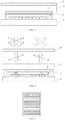
- FIG. 1 is a structural schematic diagram of an existing light-emitting diode display panel.
- the light-emitting diode display panel comprises a first substrate 1 and a second substrate 2.
- the first substrate 1 contains inherent constructions of a light-emitting diode display panel such as an anode, a cathode, a light-emitting layer, a color filter layer, a hole injection layer, a hole transporting layer, an electron transporting layer, a protective film and the like.
- the light-emitting diode display panel as illustrated in FIG. 1 is readily affected by ambient light, since a region where metal is contained in the first substrate 1 (i.e., a metallic region) reflects a 100% of the ambient light as indicated by the arrow in FIG. 1 , which has a significant impact on a light path and colors of the light-emitting diode display panel, thereby affecting the display quality.
- a common improvement approach is to provide a polarizer 3 at an outer side of the second substrate 2 as illustrated in FIG. 2 .
- the ambient light is converted into linear polarized light after passing through the polarizer 3, and exits as linear polarized light after being reflected by the metallic region with a reflective index of about 50%. While the light-emitting diode display panel has a somewhat decreased reflective index for the ambient light when being provided with the polarizer 3, about 50% of the ambient light that is reflected still has an impact on the display quality.
- the present disclosure provides a light-emitting diode display panel comprising a first substrate, a second substrate and a polarizer layer, the light-emitting diode display panel further comprising a ⁇ /4 phase retarder film.
- the polarizer layer and the ⁇ /4 phase retarder film are arranged such that incident ambient light passes in turn through the polarizer layer and the ⁇ /4 phase retarder film to arrive at the first substrate.
- an angle between a transmission axis of the polarizer layer and a transmission axis of the ⁇ /4 phase retarder film is 45°.
- the polarizer layer is arranged at a surface of the second substrate away from the first substrate, and the ⁇ /4 phase retarder film is arranged at a surface of the second substrate adjacent to the first substrate.
- the polarizer layer is a polarizer.
- the polarizer layer and the ⁇ /4 phase retarder film are arranged in turn at a surface of the second substrate adjacent to the first substrate.
- the polarizer layer is a metallic grating layer for converting the ambient light into linear polarized light.
- the polarizer layer is a dichroic dye molecule layer for converting the ambient light into linear polarized light.
- a dichroic dye molecule forming the dichroic dye molecule layer comprises at least one of an azo group dichroic dye molecule and an anthraquinonyl dichroic dye molecule.
- the ⁇ /4 phase retarder film comprises an alignment layer and a liquid crystal polymer layer arranged over the alignment layer, an angle between an alignment direction of the alignment layer and a transmission axis of the polarizer layer being 45°.
- the polarizer layer has a pattern corresponding to a pattern of a metallic region in the first substrate.
- the present disclosure also provides a method of fabricating a light-emitting diode display panel, the light-emitting diode display panel comprising a first substrate and a second substrate, the method comprising steps of:
- an angle between a transmission axis of the polarizer layer and a transmission axis of the ⁇ /4 phase retarder film is 45°.
- the present disclosure effectively prevents the impact of reflection of the ambient light on the displayed image and thus improves the display quality, by arranging both the polarizer layer and the ⁇ /4 phase retarder film in the light-emitting diode display panel.
- the present disclosure provides a light-emitting diode display panel comprising a first substrate, a second substrate and a polarizer layer, the light-emitting diode display panel further comprising a ⁇ /4 phase retarder film.
- the polarizer layer and the ⁇ /4 phase retarder film are arranged such that incident ambient light arrives at the first substrate after passing through the polarizer layer and the ⁇ /4 phase retarder film in turn.
- the light-emitting diode display panel may be an organic light-emitting diode (OLED) display panel, or it may be an active matrix organic light-emitting diode (AMOLED) display panel.
- the first substrate may be used for display, and the second substrate may be used for encapsulation of the first substrate.
- the first substrate may be a display substrate which contains constructions such as an anode, a cathode, a light-emitting layer, a color filter layer, a hole injection layer, a hole transporting layer, an electron transporting layer, an array of thin-film transistors, a protective film, and the like;
- the second substrate may be a cover plate for encapsulation purpose only.
- a plurality of constructions in the first substrate such as the anode, the cathode, the array of thin-film transistors and the like, contain metallic materials.
- a region where the metallic materials are located is referred to here as a metallic region.
- the metallic region in the first substrate can reflect ambient light incident on the first substrate, and thus has an impact on the display effect.
- the incident ambient light is converted into linear polarized light after passing through the polarizer layer, and into circular polarized light or elliptical polarized light after passing through the ⁇ /4 phase retarder film. If an angle between a transmission axis of the polarizer layer and a transmission axis of the ⁇ /4 phase retarder film is 45°, the circular polarized light is produced; otherwise the elliptical polarized light is produced. A change in handedness occurs to the circular polarized light or elliptical polarized light when it arrives at the first substrate and is reflected by the metallic region.
- left-handed circular polarized light will be converted into right-handed circular polarized light, and then into linear polarized light whose polarization is perpendicular to the previous polarization after passing again through the ⁇ /4 phase retarder film, and thus it cannot transmit through the polarizer layer. Therefore, the impact of reflection of the ambient light on the displayed image is significantly reduced, resulting in an improved display quality.
- the angle between the transmission axis of the polarizer layer and the transmission axis of the ⁇ /4 phase retarder film is 45°.
- the exiting ambient light comprises only linear polarized light whose polarization is perpendicular to the transmission axis of the polarizer layer, such that no ambient light can transmit through the polarizer layer, i.e. a reflective index of the incident ambient light is 0%, leading to avoidance of the impact of the ambient light on the display quality.
- FIG. 3 is a structural schematic diagram of a light-emitting diode display panel according to an embodiment of the present disclosure.
- the polarizer layer 6 is arranged at a surface of the second substrate 2 away from the first substrate 1 (i.e., at an outer side of the second substrate 2), and the ⁇ /4 phase retarder film 7 is arranged at a surface of the second substrate 2 adjacent to the first substrate 1 (i.e., at an inner side of the second substrate 2).
- the ambient light is incident from above the polarizer layer 6 and passes in turn through the polarizer layer 6, the second substrate 2 and the ⁇ /4 phase retarder film 7 to shine on the first substrate 1.
- the polarizer layer 6 in this embodiment is not limited to any specific form, as long as it can convert the ambient light into linear polarized light.
- the polarizer layer 6 in FIG. 3 is arranged at the outer side of the second substrate 2, in which case the polarizer layer 6 is preferably a conventional polarizer so as to simplify the manufacture procedure and to save the cost.
- the ⁇ /4 phase retarder film 7 may be achieved by forming an alignment layer 4 and a liquid crystal polymer layer 5 in turn at the inner side of the second substrate 2. With the angle between the transmission axis of the polarizer layer 6 and the transmission axis of the ⁇ /4 phase retarder film 7 being preferably 45°, an angle between an alignment direction of the alignment layer 4 and the transmission axis of the polarizer layer 6 may be arranged to be 45°.
- the alignment layer 4 may be formed by way of friction, or it may be formed by way of photo-induced alignment.
- the liquid crystal polymer layer 5 is formed by liquid crystal reactive monomers through ultraviolet curing.
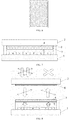
- FIG. 4 is a schematic diagram of a light path of the construction as shown in FIG. 3 .
- the transmission axis of the polarizer layer 6 is at 0°, then the incident ambient light is converted into linear polarized light of 0° after passing through the polarizer layer 6 as shown in FIG. 5 .
- the transmission axis of the ⁇ /4 phase retarder film 7 is preferably orientated at 45° to form an angle of 45° with the transmission axis of the polarizer layer 6.
- the alignment direction of the alignment layer 4 may be arranged to be 45°, and then the liquid crystal polymer layer 5 may be arranged over the alignment layer 4.
- a plan view of the arranged liquid crystal polymer layer 5 is shown in FIG. 6 .
- the linear polarized light of 0° is converted into left-handed circular polarized light.
- the left-handed circular polarized light is then converted into right-handed circular polarized light upon reflection by the metallic region in the first substrate 1.
- the right-handed circular polarized light is converted into linear polarized light of 90° that cannot transmit through the polarizer layer 6 with a transmission axis of 0°, resulting in a reflective index of 0% against the incident ambient light. This eliminates the impact of reflection of the ambient light on the display effect of the display panel, and hence improves the display quality.
- FIG. 7 is a schematic diagram of a light-emitting diode display panel according to another embodiment of the present disclosure.
- the polarizer layer 6 and the ⁇ /4 phase retarder film 7 are arranged in turn at a surface of the second substrate 2 adjacent to the first substrate 1 (i.e., at the inner side of the second substrate 2).
- the ambient light is incident from above the second substrate 2, passing in turn through the second substrate 2, the polarizer layer 6 and the ⁇ /4 phase retarder film 7 to shine on the first substrate 1.
- the polarizer layer 6 in this embodiment is not limited to any specific form, as long as it can convert the ambient light into linear polarized light.
- the polarizer layer 6 in FIG. 7 is arranged at the inner side of the second substrate 2, in which case the polarizer layer 6 is preferably a metallic grating layer or dichroic dye molecule layer capable of converting the ambient light into linear polarized light.
- a thin metallic grating layer or dichroic dye molecule layer facilitates restriction of the thickness of the display panel as a whole, allowing it to be in line with the trend of light weight.
- a dichroic dye molecule For a dichroic dye molecule, it can absorb one of the two orthogonal components of the linear polarization in the incident ambient light, allowing the other one to transmit. Therefore, the dichroic dye molecule layer may achieve a function of light conversion in place of a polarizer.
- a dichroic dye molecule forming the dichroic dye molecule layer may be any of an azo group dichroic dye molecule and an anthraquinonyl dichroic dye molecule or combination thereof.
- the ⁇ /4 phase retarder film 7 can be achieved by forming in turn the alignment layer 4 and the liquid crystal polymer layer 5 over the polarizer layer 6.
- the angle between the transmission axis of the polarizer layer 6 and the transmission axis of the ⁇ /4 phase retarder film 7 being preferably 45°
- the angle between the alignment direction of the alignment layer 4 and the transmission axis of the polarizer layer 6 may be arranged to be 45°.
- the alignment layer 4 may be formed by way of friction, or it may be formed by way of photo-induced alignment.
- the liquid crystal polymer layer 5 is formed by liquid crystal reactive monomers through ultraviolet curing.
- FIG. 8 is a schematic diagram of a light path of the construction as shown in FIG. 7 .
- the transmission axis of the polarizer layer 6 is at 0°
- the incident ambient light is converted into linear polarized light of 0° after passing through the polarizer layer 6.
- the transmission axis of the ⁇ /4 phase retarder film 7 is preferably orientated at 45° to form an angle of 45° with the transmission axis of the polarizer layer 6.
- the alignment direction of the alignment layer 4 may be arranged to be 45°, and then the liquid crystal polymer layer 5 may be arranged over the alignment layer 4, forming the ⁇ /4 phase retarder film 7 with a transmission axis of 45°.
- the linear polarized light of 0° is converted into left-handed circular polarized light.
- the left-handed circular polarized light is then converted into right-handed circular polarized light upon reflection by the metallic region in the first substrate 1.
- the right-handed circular polarized light is converted into linear polarized light of 90° that cannot transmit through the polarizer layer 6 with a transmission axis of 0°, resulting in a reflective index of 0% against the incident ambient light. This eliminates the impact of reflection of the ambient light on the display effect of the display panel, and hence improves the display quality.
- the arrangement of the ⁇ /4 phase retarder film and the polarizer layer is not limited to any specific configuration, as long as the ambient light passes in turn through the polarizer layer and the ⁇ /4 phase retarder film to arrive at the first substrate or the metallic region therein.
- the ⁇ /4 phase retarder film and the polarizer layer may also be arranged in turn at the outer side of the second substrate, i.e., the ⁇ /4 phase retarder film is firstly arranged at the outer side of the second substrate, and then the polarizer layer is arranged at outer side of the ⁇ /4 phase retarder film.
- the principle of the light path is the same as the above-mentioned two embodiments, which will not be discussed here in detail.
- the polarizer layer is arranged at the outer side of the second substrate, it is preferably in a form of a polarizer.
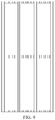
- the polarizer layer in the present disclosure may be that which has a pattern corresponding to a pattern of the metallic region in the first substrate.
- a plurality of constructions in the first substrate such as the anode, the cathode, the array of thin-film transistors and the like, contain metallic materials, with the region where the metallic materials are located being referred to as the metallic region.
- the metallic region generally has a predetermined pattern. Where the pattern of the polarizer layer corresponds to the pattern of the metallic region in the first substrate, a brightness of the display panel can be increased, and materials for fabricating the polarizer layer can be saved.
- the pattern of the polarizer layer may correspond to the pattern of a metallic region formed by metallic material in a certain layered construction of the first substrate, or it may correspond to an accumulation of patterns of the metallic regions formed by all the metallic materials in the first substrate.
- FIG. 9 is a plan view of a polarizer layer having a pattern, in which the pattern of the polarizer layer corresponds to a periphery of a display region, and to a metallic region formed by the metallic electrodes in the array of thin-film transistors.
- the present disclosure also provides in another aspect a method of fabricating the above-mentioned light-emitting diode display panel, the light-emitting diode display panel comprising a first substrate and a second substrate, the method comprising steps of:
- an angle between a transmission axis of the polarizer layer and a transmission axis of the ⁇ /4 phase retarder film is 45°.
- the incident ambient light is converted into linear polarized light after passing through the polarizer layer, and into circular polarized light after passing through the ⁇ /4 phase retarder film.
- a change in handedness occurs to the circular polarized light when it arrives at the first substrate and is reflected by a metallic region in the first substrate.
- left-handed circular polarized light will be converted into right-handed circular polarized light, and then into linear polarized light whose polarization is perpendicular to the previous polarization after passing again through the ⁇ /4 phase retarder film, and thus it cannot transmit through the polarizer layer.
- the present disclosure effectively reduces the impact of reflection of the ambient light on the displayed image, resulting in an improved display quality.
- the polarizer layer may be a polarizer, a metallic grating layer, a dichroic dye molecule layer, or any other layered construction that is able to convert the ambient light into linear polarized light.
- the polarizer layer is arranged at the outer side of the second substrate, it is preferably a polarizer for purpose of a reduced difficulty of process and a saved cost.
- the polarizer layer is arranged at the inner side of the second substrate, it is preferably a metallic grating layer or a dichroic dye molecule layer so as to maintain the thickness of the display panel at a low level.
- the ⁇ /4 phase retarder film may comprise an alignment layer and a liquid crystal polymer layer arranged over the alignment layer, with the liquid crystal polymer layer formed by liquid crystal reactive monomers through ultraviolet curing.
- an angle between an alignment direction of the alignment layer and a transmission axis of the polarized layer is 45°.
- the present disclosure effectively prevents the impact of reflection of the ambient light on the displayed image and thus improves the display quality, by arranging both the polarizer layer and the ⁇ /4 phase retarder film in the light-emitting diode display panel.
Landscapes
- Physics & Mathematics (AREA)
- Optics & Photonics (AREA)
- General Physics & Mathematics (AREA)
- Chemical & Material Sciences (AREA)
- Crystallography & Structural Chemistry (AREA)
- Engineering & Computer Science (AREA)
- Manufacturing & Machinery (AREA)
- Electroluminescent Light Sources (AREA)
- Polarising Elements (AREA)
- Devices For Indicating Variable Information By Combining Individual Elements (AREA)
Abstract
Description
- The present disclosure relates to the field of display technology, and more particularly to a light-emitting diode display panel and a method of fabricating same.
- The light-emitting diode display panel stands for a trend for development of display products, especially the organic light-emitting display panel, which has a range of advantages such as being wide in viewing angle, fast in response speed, high in brightness, high in contrast, bright in colors, light in weight, thin in thickness, low in power consumption, and the like.
-
FIG. 1 is a structural schematic diagram of an existing light-emitting diode display panel. The light-emitting diode display panel comprises afirst substrate 1 and asecond substrate 2. Thefirst substrate 1 contains inherent constructions of a light-emitting diode display panel such as an anode, a cathode, a light-emitting layer, a color filter layer, a hole injection layer, a hole transporting layer, an electron transporting layer, a protective film and the like. The light-emitting diode display panel as illustrated inFIG. 1 is readily affected by ambient light, since a region where metal is contained in the first substrate 1 (i.e., a metallic region) reflects a 100% of the ambient light as indicated by the arrow inFIG. 1 , which has a significant impact on a light path and colors of the light-emitting diode display panel, thereby affecting the display quality. - At present, a common improvement approach is to provide a
polarizer 3 at an outer side of thesecond substrate 2 as illustrated inFIG. 2 . The ambient light is converted into linear polarized light after passing through thepolarizer 3, and exits as linear polarized light after being reflected by the metallic region with a reflective index of about 50%. While the light-emitting diode display panel has a somewhat decreased reflective index for the ambient light when being provided with thepolarizer 3, about 50% of the ambient light that is reflected still has an impact on the display quality. - It is an object of the present disclosure to provide a light-emitting diode display panel and a method of fabricating the same to reduce an impact of ambient light on display quality.
- To address this, the present disclosure provides a light-emitting diode display panel comprising a first substrate, a second substrate and a polarizer layer, the light-emitting diode display panel further comprising a λ/4 phase retarder film. The polarizer layer and the λ/4 phase retarder film are arranged such that incident ambient light passes in turn through the polarizer layer and the λ/4 phase retarder film to arrive at the first substrate.
- Preferably, an angle between a transmission axis of the polarizer layer and a transmission axis of the λ/4 phase retarder film is 45°.
- Preferably, the polarizer layer is arranged at a surface of the second substrate away from the first substrate, and the λ/4 phase retarder film is arranged at a surface of the second substrate adjacent to the first substrate.
- Preferably, the polarizer layer is a polarizer.
- Preferably, the polarizer layer and the λ/4 phase retarder film are arranged in turn at a surface of the second substrate adjacent to the first substrate.
- Preferably, the polarizer layer is a metallic grating layer for converting the ambient light into linear polarized light.
- Preferably, the polarizer layer is a dichroic dye molecule layer for converting the ambient light into linear polarized light.
- Preferably, a dichroic dye molecule forming the dichroic dye molecule layer comprises at least one of an azo group dichroic dye molecule and an anthraquinonyl dichroic dye molecule.
- Preferably, the λ/4 phase retarder film comprises an alignment layer and a liquid crystal polymer layer arranged over the alignment layer, an angle between an alignment direction of the alignment layer and a transmission axis of the polarizer layer being 45°.
- Preferably, the polarizer layer has a pattern corresponding to a pattern of a metallic region in the first substrate.
- The present disclosure also provides a method of fabricating a light-emitting diode display panel, the light-emitting diode display panel comprising a first substrate and a second substrate, the method comprising steps of:
- arranging a polarizer layer at a surface of the second substrate away from the first substrate, and arranging a λ/4 phase retarder film at a surface of the second substrate adjacent to the first substrate;
- or, arranging a polarizer layer and a λ/4 phase retarder film in turn at a surface of the second substrate adjacent to the first substrate;
- or, arranging a λ/4 phase retarder film and a polarizer layer in turn at a surface of the second substrate away from the first substrate; and
- cutting the second substrate and the first substrate for cell alignment;
- wherein the polarizer layer and the λ/4 phase retarder film are arranged such that incident ambient light passes in turn through the polarizer layer and the λ/4 phase retarder film to arrive at the first substrate.
- Preferably, an angle between a transmission axis of the polarizer layer and a transmission axis of the λ/4 phase retarder film is 45°.
- The present disclosure effectively prevents the impact of reflection of the ambient light on the displayed image and thus improves the display quality, by arranging both the polarizer layer and the λ/4 phase retarder film in the light-emitting diode display panel.
- The accompanying drawings are provided for a better understanding of the present disclosure, which form a part of the specification for illustration and not limitation of the present disclosure in connection with the detailed description below. In the drawings:
-
FIG. 1 is a structural schematic diagram of an existing light-emitting diode display panel; -
FIG. 2 is a structural schematic diagram of another existing light-emitting diode display panel; -
FIG. 3 is a structural schematic diagram of a light-emitting diode display panel according to an embodiment of the present disclosure; -
FIG. 4 is a schematic diagram of a light path of the construction as shown inFIG. 3 ; -
FIG. 5 is a plan view of a polarizer layer ofFIG. 3 ; -
FIG. 6 is a plan view of a liquid crystal polymer layer ofFIG. 3 ; -
FIG. 7 is a structural schematic diagram of a light-emitting diode display panel according to another embodiment of the present disclosure; -
FIG. 8 is a schematic diagram of a light path of the construction as shown inFIG. 7 ; and -
FIG. 9 is a plan view of a polarizer layer having a pattern. - Embodiments of the present disclosure are described in detail in connection with the accompanying drawings. It is to be understood that the described embodiments herein are for illustration and explanation purposes only, and not for limitation of the present disclosure.
- The present disclosure provides a light-emitting diode display panel comprising a first substrate, a second substrate and a polarizer layer, the light-emitting diode display panel further comprising a λ/4 phase retarder film. The polarizer layer and the λ/4 phase retarder film are arranged such that incident ambient light arrives at the first substrate after passing through the polarizer layer and the λ/4 phase retarder film in turn.
- Here the light-emitting diode display panel may be an organic light-emitting diode (OLED) display panel, or it may be an active matrix organic light-emitting diode (AMOLED) display panel. In the disclosure, the first substrate may be used for display, and the second substrate may be used for encapsulation of the first substrate. For example, the first substrate may be a display substrate which contains constructions such as an anode, a cathode, a light-emitting layer, a color filter layer, a hole injection layer, a hole transporting layer, an electron transporting layer, an array of thin-film transistors, a protective film, and the like; the second substrate may be a cover plate for encapsulation purpose only. Therein, a plurality of constructions in the first substrate, such as the anode, the cathode, the array of thin-film transistors and the like, contain metallic materials. A region where the metallic materials are located is referred to here as a metallic region. The metallic region in the first substrate can reflect ambient light incident on the first substrate, and thus has an impact on the display effect.
- In the present disclosure, the incident ambient light is converted into linear polarized light after passing through the polarizer layer, and into circular polarized light or elliptical polarized light after passing through the λ/4 phase retarder film. If an angle between a transmission axis of the polarizer layer and a transmission axis of the λ/4 phase retarder film is 45°, the circular polarized light is produced; otherwise the elliptical polarized light is produced. A change in handedness occurs to the circular polarized light or elliptical polarized light when it arrives at the first substrate and is reflected by the metallic region. For example, left-handed circular polarized light will be converted into right-handed circular polarized light, and then into linear polarized light whose polarization is perpendicular to the previous polarization after passing again through the λ/4 phase retarder film, and thus it cannot transmit through the polarizer layer. Therefore, the impact of reflection of the ambient light on the displayed image is significantly reduced, resulting in an improved display quality.
- Preferably, the angle between the transmission axis of the polarizer layer and the transmission axis of the λ/4 phase retarder film is 45°. In this case, the exiting ambient light comprises only linear polarized light whose polarization is perpendicular to the transmission axis of the polarizer layer, such that no ambient light can transmit through the polarizer layer, i.e. a reflective index of the incident ambient light is 0%, leading to avoidance of the impact of the ambient light on the display quality.
-
FIG. 3 is a structural schematic diagram of a light-emitting diode display panel according to an embodiment of the present disclosure. InFIG. 3 , thepolarizer layer 6 is arranged at a surface of thesecond substrate 2 away from the first substrate 1 (i.e., at an outer side of the second substrate 2), and the λ/4phase retarder film 7 is arranged at a surface of thesecond substrate 2 adjacent to the first substrate 1 (i.e., at an inner side of the second substrate 2). The ambient light is incident from above thepolarizer layer 6 and passes in turn through thepolarizer layer 6, thesecond substrate 2 and the λ/4phase retarder film 7 to shine on thefirst substrate 1. - The
polarizer layer 6 in this embodiment is not limited to any specific form, as long as it can convert the ambient light into linear polarized light. Thepolarizer layer 6 inFIG. 3 is arranged at the outer side of thesecond substrate 2, in which case thepolarizer layer 6 is preferably a conventional polarizer so as to simplify the manufacture procedure and to save the cost. - The λ/4
phase retarder film 7 may be achieved by forming analignment layer 4 and a liquidcrystal polymer layer 5 in turn at the inner side of thesecond substrate 2. With the angle between the transmission axis of thepolarizer layer 6 and the transmission axis of the λ/4phase retarder film 7 being preferably 45°, an angle between an alignment direction of thealignment layer 4 and the transmission axis of thepolarizer layer 6 may be arranged to be 45°. - The
alignment layer 4 may be formed by way of friction, or it may be formed by way of photo-induced alignment. The liquidcrystal polymer layer 5 is formed by liquid crystal reactive monomers through ultraviolet curing. -
FIG. 4 is a schematic diagram of a light path of the construction as shown inFIG. 3 . Assuming that the transmission axis of thepolarizer layer 6 is at 0°, then the incident ambient light is converted into linear polarized light of 0° after passing through thepolarizer layer 6 as shown inFIG. 5 . The transmission axis of the λ/4phase retarder film 7 is preferably orientated at 45° to form an angle of 45° with the transmission axis of thepolarizer layer 6. Here the alignment direction of thealignment layer 4 may be arranged to be 45°, and then the liquidcrystal polymer layer 5 may be arranged over thealignment layer 4. A plan view of the arranged liquidcrystal polymer layer 5 is shown inFIG. 6 . - Upon passing through the λ/4
phase retarder film 7 formed by thealignment layer 4 and the liquidcrystal polymer layer 5, the linear polarized light of 0° is converted into left-handed circular polarized light. The left-handed circular polarized light is then converted into right-handed circular polarized light upon reflection by the metallic region in thefirst substrate 1. Upon passing again through the λ/4phase retarder film 7, the right-handed circular polarized light is converted into linear polarized light of 90° that cannot transmit through thepolarizer layer 6 with a transmission axis of 0°, resulting in a reflective index of 0% against the incident ambient light. This eliminates the impact of reflection of the ambient light on the display effect of the display panel, and hence improves the display quality. -
FIG. 7 is a schematic diagram of a light-emitting diode display panel according to another embodiment of the present disclosure. InFIG. 7 , thepolarizer layer 6 and the λ/4phase retarder film 7 are arranged in turn at a surface of thesecond substrate 2 adjacent to the first substrate 1 (i.e., at the inner side of the second substrate 2). The ambient light is incident from above thesecond substrate 2, passing in turn through thesecond substrate 2, thepolarizer layer 6 and the λ/4phase retarder film 7 to shine on thefirst substrate 1. - The
polarizer layer 6 in this embodiment is not limited to any specific form, as long as it can convert the ambient light into linear polarized light. Thepolarizer layer 6 inFIG. 7 is arranged at the inner side of thesecond substrate 2, in which case thepolarizer layer 6 is preferably a metallic grating layer or dichroic dye molecule layer capable of converting the ambient light into linear polarized light. A thin metallic grating layer or dichroic dye molecule layer facilitates restriction of the thickness of the display panel as a whole, allowing it to be in line with the trend of light weight. - For a dichroic dye molecule, it can absorb one of the two orthogonal components of the linear polarization in the incident ambient light, allowing the other one to transmit. Therefore, the dichroic dye molecule layer may achieve a function of light conversion in place of a polarizer. In the present disclosure, a dichroic dye molecule forming the dichroic dye molecule layer may be any of an azo group dichroic dye molecule and an anthraquinonyl dichroic dye molecule or combination thereof.
- The molecular formula of the azo group dichroic dye molecule is shown as follows:

- The molecular formula of the anthraquinonyl dichroic dye molecule is shown as follows:

- In the embodiment as shown in
FIG. 7 , the λ/4phase retarder film 7 can be achieved by forming in turn thealignment layer 4 and the liquidcrystal polymer layer 5 over thepolarizer layer 6. With the angle between the transmission axis of thepolarizer layer 6 and the transmission axis of the λ/4phase retarder film 7 being preferably 45°, the angle between the alignment direction of thealignment layer 4 and the transmission axis of thepolarizer layer 6 may be arranged to be 45°. - Likewise, the
alignment layer 4 may be formed by way of friction, or it may be formed by way of photo-induced alignment. The liquidcrystal polymer layer 5 is formed by liquid crystal reactive monomers through ultraviolet curing. -
FIG. 8 is a schematic diagram of a light path of the construction as shown inFIG. 7 . Assuming that the transmission axis of thepolarizer layer 6 is at 0°, then the incident ambient light is converted into linear polarized light of 0° after passing through thepolarizer layer 6. The transmission axis of the λ/4phase retarder film 7 is preferably orientated at 45° to form an angle of 45° with the transmission axis of thepolarizer layer 6. Here the alignment direction of thealignment layer 4 may be arranged to be 45°, and then the liquidcrystal polymer layer 5 may be arranged over thealignment layer 4, forming the λ/4phase retarder film 7 with a transmission axis of 45°. - Upon passing through the λ/4
phase retarder film 7 formed by thealignment layer 4 and the liquidcrystal polymer layer 5, the linear polarized light of 0° is converted into left-handed circular polarized light. The left-handed circular polarized light is then converted into right-handed circular polarized light upon reflection by the metallic region in thefirst substrate 1. Upon passing again through the λ/4phase retarder film 7, the right-handed circular polarized light is converted into linear polarized light of 90° that cannot transmit through thepolarizer layer 6 with a transmission axis of 0°, resulting in a reflective index of 0% against the incident ambient light. This eliminates the impact of reflection of the ambient light on the display effect of the display panel, and hence improves the display quality. - In the present disclosure, the arrangement of the λ/4 phase retarder film and the polarizer layer is not limited to any specific configuration, as long as the ambient light passes in turn through the polarizer layer and the λ/4 phase retarder film to arrive at the first substrate or the metallic region therein. For example, the λ/4 phase retarder film and the polarizer layer may also be arranged in turn at the outer side of the second substrate, i.e., the λ/4 phase retarder film is firstly arranged at the outer side of the second substrate, and then the polarizer layer is arranged at outer side of the λ/4 phase retarder film. The principle of the light path is the same as the above-mentioned two embodiments, which will not be discussed here in detail. Furthermore, since the polarizer layer is arranged at the outer side of the second substrate, it is preferably in a form of a polarizer.
- Further, the polarizer layer in the present disclosure may be that which has a pattern corresponding to a pattern of the metallic region in the first substrate. As mentioned above, a plurality of constructions in the first substrate, such as the anode, the cathode, the array of thin-film transistors and the like, contain metallic materials, with the region where the metallic materials are located being referred to as the metallic region. The metallic region generally has a predetermined pattern. Where the pattern of the polarizer layer corresponds to the pattern of the metallic region in the first substrate, a brightness of the display panel can be increased, and materials for fabricating the polarizer layer can be saved.
- In the present disclosure, the pattern of the polarizer layer may correspond to the pattern of a metallic region formed by metallic material in a certain layered construction of the first substrate, or it may correspond to an accumulation of patterns of the metallic regions formed by all the metallic materials in the first substrate. For example,
FIG. 9 is a plan view of a polarizer layer having a pattern, in which the pattern of the polarizer layer corresponds to a periphery of a display region, and to a metallic region formed by the metallic electrodes in the array of thin-film transistors. - The present disclosure also provides in another aspect a method of fabricating the above-mentioned light-emitting diode display panel, the light-emitting diode display panel comprising a first substrate and a second substrate, the method comprising steps of:
- S1: arranging a polarizer layer at a surface of the second substrate away from the first substrate (i.e., at an outer side of the second substrate), and arranging a λ/4 phase retarder film at a surface of the second substrate adjacent to the first substrate (i.e., at an inner side of the second substrate);
or, arranging a polarizer layer and a λ/4 phase retarder film in turn at an inner side of the second substrate;
or, arranging a λ/4 phase retarder film and a polarizer layer in turn at an outer side of the second substrate; and - S2: cutting the second substrate and the first substrate for cell alignment;
wherein the polarizer layer and the λ/4 phase retarder film are arranged such that incident ambient light passes in turn through the polarizer layer and the λ/4 phase retarder film to arrive at the first substrate. - Preferably, an angle between a transmission axis of the polarizer layer and a transmission axis of the λ/4 phase retarder film is 45°.
- The incident ambient light is converted into linear polarized light after passing through the polarizer layer, and into circular polarized light after passing through the λ/4 phase retarder film. A change in handedness occurs to the circular polarized light when it arrives at the first substrate and is reflected by a metallic region in the first substrate. For example, left-handed circular polarized light will be converted into right-handed circular polarized light, and then into linear polarized light whose polarization is perpendicular to the previous polarization after passing again through the λ/4 phase retarder film, and thus it cannot transmit through the polarizer layer. The present disclosure effectively reduces the impact of reflection of the ambient light on the displayed image, resulting in an improved display quality.
- The polarizer layer may be a polarizer, a metallic grating layer, a dichroic dye molecule layer, or any other layered construction that is able to convert the ambient light into linear polarized light. In case the polarizer layer is arranged at the outer side of the second substrate, it is preferably a polarizer for purpose of a reduced difficulty of process and a saved cost. In case the polarizer layer is arranged at the inner side of the second substrate, it is preferably a metallic grating layer or a dichroic dye molecule layer so as to maintain the thickness of the display panel at a low level.
- The λ/4 phase retarder film may comprise an alignment layer and a liquid crystal polymer layer arranged over the alignment layer, with the liquid crystal polymer layer formed by liquid crystal reactive monomers through ultraviolet curing. Preferably, an angle between an alignment direction of the alignment layer and a transmission axis of the polarized layer is 45°.
- The present disclosure effectively prevents the impact of reflection of the ambient light on the displayed image and thus improves the display quality, by arranging both the polarizer layer and the λ/4 phase retarder film in the light-emitting diode display panel.
- It is to be understood that the embodiments above are exemplary embodiments for illustration of the principle of the present disclosure only; however, the present disclosure is not limited thereto. Various variations and modifications can be made by the skilled in the art without departing from the spirit and scope of the present disclosure, which are considered within the protection scope of the present disclosure.
Claims (12)
- A light-emitting diode display panel comprising a first substrate, a second substrate, and a polarizer layer, wherein the light-emitting diode display panel further comprises a λ/4 phase retarder film, the polarizer layer and the λ/4 phase retarder film being arranged such that incident ambient light passes in turn through the polarizer layer and the λ/4 phase retarder film to arrive at the first substrate.
- The light-emitting diode display panel as recited in claim 1, wherein an angle between a transmission axis of the polarizer layer and a transmission axis of the λ/4 phase retarder film is 45°.
- The light-emitting diode display panel as recited in claim 1 or 2, wherein the polarizer layer is arranged at a surface of the second substrate away from the first substrate, and the λ/4 phase retarder film is arranged at a surface of the second substrate adjacent to the first substrate.
- The light-emitting diode display panel as recited in claim 3, wherein the polarizer layer is a polarizer.
- The light-emitting diode display panel as recited in claim 1 or 2, wherein the polarizer layer and the λ/4 phase retarder film are arranged in turn at a surface of the second substrate adjacent to the first substrate.
- The light-emitting diode display panel as recited in claim 5, wherein the polarizer layer is a metallic grating layer for converting the ambient light into linear polarized light.
- The light-emitting diode display panel as recited in claim 5, wherein the polarizer layer is a dichroic dye molecule layer for converting the ambient light into linear polarized light.
- The light-emitting diode display panel as recited in claim 7, wherein a dichroic dye molecule forming the dichroic dye molecule layer comprises at least one of an azo group dichroic dye molecule and an anthraquinonyl dichroic dye molecule.
- The light-emitting diode display panel as recited in any of claims 1 to 8, wherein the λ/4 phase retarder film comprises an alignment layer and a liquid crystal polymer layer arranged over the alignment layer, an angle between an alignment direction of the alignment layer and a transmission axis of the polarizer layer being 45°.
- The light-emitting diode display panel as recited in any of claims 1 to 9, wherein the polarizer layer has a pattern corresponding to a pattern of a metallic region in the first substrate.
- A method of fabricating a light-emitting diode display panel, the light-emitting diode display panel comprising a first substrate and a second substrate, the method comprising steps of:S1: arranging a polarizer layer at a surface of the second substrate away from the first substrate, and arranging a λ/4 phase retarder film at a surface of the second substrate adjacent to the first substrate;
or, arranging a polarizer layer and a λ/4 phase retarder film in turn at a surface of the second substrate adjacent to the first substrate;
or, arranging a λ/4 phase retarder film and a polarizer layer in turn at a surface of the second substrate away from the first substrate; andS2: cutting the second substrate and the first substrate for cell alignment;
wherein the polarizer layer and the λ/4 phase retarder film are arranged such that incident ambient light passes in turn through the polarizer layer and the λ/4 phase retarder film to arrive at the first substrate. - The method as recited in claim 11, wherein an angle between a transmission axis of the polarizer layer and a transmission axis of the λ/4 phase retarder film is 45°.
Applications Claiming Priority (2)
| Application Number | Priority Date | Filing Date | Title |
|---|---|---|---|
| CN201410492129.9A CN104319282B (en) | 2014-09-23 | 2014-09-23 | LED display panel |
| PCT/CN2015/070616 WO2016045260A1 (en) | 2014-09-23 | 2015-01-13 | Light-emitting diode display panel and manufacturing method therefor |
Publications (3)
| Publication Number | Publication Date |
|---|---|
| EP3200233A1 true EP3200233A1 (en) | 2017-08-02 |
| EP3200233A4 EP3200233A4 (en) | 2018-06-06 |
| EP3200233B1 EP3200233B1 (en) | 2019-07-03 |
Family
ID=52374491
Family Applications (1)
| Application Number | Title | Priority Date | Filing Date |
|---|---|---|---|
| EP15793671.7A Active EP3200233B1 (en) | 2014-09-23 | 2015-01-13 | Light-emitting diode display panel and manufacturing method therefor |
Country Status (4)
| Country | Link |
|---|---|
| US (1) | US20160329527A1 (en) |
| EP (1) | EP3200233B1 (en) |
| CN (1) | CN104319282B (en) |
| WO (1) | WO2016045260A1 (en) |
Families Citing this family (15)
| Publication number | Priority date | Publication date | Assignee | Title |
|---|---|---|---|---|
| JP6510655B2 (en) * | 2015-09-03 | 2019-05-08 | 富士フイルム株式会社 | Organic electroluminescent display |
| CN105510999B (en) | 2016-01-28 | 2019-05-28 | 京东方科技集团股份有限公司 | Anti-reflection structure and its manufacturing method, display and its manufacturing method |
| CN106249336A (en) * | 2016-08-04 | 2016-12-21 | 深圳市华星光电技术有限公司 | Rotatory polarization sheet and OLED display |
| CN107065180A (en) * | 2017-01-17 | 2017-08-18 | 浙江唯见科技有限公司 | A kind of close-coupled virtual reality near-eye display system and wear display device |
| CN107219723B (en) * | 2017-08-02 | 2021-01-22 | 京东方科技集团股份有限公司 | Manufacturing method of metal grating, metal grating and display device |
| CN109656053B (en) * | 2017-09-22 | 2021-10-08 | 出门问问信息科技有限公司 | Display device, display control method, and electronic equipment |
| CN108878671A (en) * | 2018-07-05 | 2018-11-23 | 武汉华星光电半导体显示技术有限公司 | OLED encapsulating structure, OLED display panel and preparation method thereof |
| CN110767105B (en) * | 2018-07-27 | 2021-01-22 | 京东方科技集团股份有限公司 | A display module and display device |
| TWI676851B (en) * | 2018-08-22 | 2019-11-11 | 隆達電子股份有限公司 | Pixel array package structure and display panel |
| US10811396B2 (en) | 2019-01-20 | 2020-10-20 | Lextar Electronics Corporation | Display device |
| CN113228287A (en) * | 2019-11-26 | 2021-08-06 | 重庆康佳光电技术研究院有限公司 | Display module, method for manufacturing display module, and electronic device |
| CN113594217B (en) * | 2021-07-29 | 2023-11-14 | 合肥维信诺科技有限公司 | Display panel, preparation method thereof and display device |
| WO2023028787A1 (en) * | 2021-08-30 | 2023-03-09 | 京东方科技集团股份有限公司 | Display substrate and display device |
| CN114094026A (en) * | 2021-11-12 | 2022-02-25 | 京东方科技集团股份有限公司 | Display panel and display device |
| CN116819823A (en) * | 2023-06-30 | 2023-09-29 | 联想(北京)有限公司 | Liquid crystal display panel |
Family Cites Families (19)
| Publication number | Priority date | Publication date | Assignee | Title |
|---|---|---|---|---|
| US6111697A (en) * | 1998-01-13 | 2000-08-29 | 3M Innovative Properties Company | Optical device with a dichroic polarizer and a multilayer optical film |
| KR100855884B1 (en) * | 2001-12-24 | 2008-09-03 | 엘지디스플레이 주식회사 | Align key for liquid crystal display |
| JP4027164B2 (en) * | 2002-06-21 | 2007-12-26 | 株式会社日立製作所 | Display device |
| JP4184189B2 (en) * | 2003-08-13 | 2008-11-19 | 株式会社 日立ディスプレイズ | Light-emitting display device |
| US8072552B2 (en) * | 2005-08-19 | 2011-12-06 | Reald Inc. | Stereoscopic eyewear |
| WO2008081941A1 (en) * | 2007-01-05 | 2008-07-10 | Asahi Glass Co., Ltd. | Wavelength selecting wavelength plate and optical head device using it |
| KR101106294B1 (en) * | 2008-05-22 | 2012-01-18 | 주식회사 엘지화학 | Brightness Enhancing Polarizer for Organic Light Emitting Diode |
| KR101415252B1 (en) * | 2008-07-22 | 2014-07-04 | 삼성디스플레이 주식회사 | Organic light emitting diode display |
| KR101571091B1 (en) * | 2008-08-26 | 2015-11-24 | 삼성디스플레이 주식회사 | Manufacturing method of organic light emitting diode display |
| KR100953656B1 (en) * | 2009-01-09 | 2010-04-20 | 삼성모바일디스플레이주식회사 | Organic light emitting diode display |
| KR20100082557A (en) * | 2009-01-09 | 2010-07-19 | 삼성모바일디스플레이주식회사 | Organic light emitting diode display |
| KR100995067B1 (en) * | 2009-01-21 | 2010-11-18 | 삼성모바일디스플레이주식회사 | Organic light emitting display |
| KR101029998B1 (en) * | 2009-12-22 | 2011-04-20 | 삼성모바일디스플레이주식회사 | Polarizing film and organic light emitting display device having same |
| KR20120004862A (en) * | 2010-07-07 | 2012-01-13 | 삼성모바일디스플레이주식회사 | Organic light emitting display |
| WO2012067080A1 (en) * | 2010-11-18 | 2012-05-24 | 日本電気株式会社 | Light source unit and projection display device provided with same |
| US8796704B2 (en) * | 2011-05-02 | 2014-08-05 | Innolux Corporation | Emissive display having polarizer and retarder films |
| DE102011056836B4 (en) * | 2011-06-22 | 2020-12-24 | Lg Display Co., Ltd. | Organic light emitting display device |
| CN102436071B (en) * | 2011-12-29 | 2013-12-04 | 昆山龙腾光电有限公司 | Stereo display device |
| TW201340773A (en) * | 2012-03-16 | 2013-10-01 | Au Optronics Corp | Mirror-switchable organic light-emitting display and mirror-switchable display |
-
2014
- 2014-09-23 CN CN201410492129.9A patent/CN104319282B/en not_active Expired - Fee Related
-
2015
- 2015-01-13 WO PCT/CN2015/070616 patent/WO2016045260A1/en not_active Ceased
- 2015-01-13 US US14/777,576 patent/US20160329527A1/en not_active Abandoned
- 2015-01-13 EP EP15793671.7A patent/EP3200233B1/en active Active
Also Published As
| Publication number | Publication date |
|---|---|
| WO2016045260A1 (en) | 2016-03-31 |
| EP3200233A4 (en) | 2018-06-06 |
| CN104319282A (en) | 2015-01-28 |
| US20160329527A1 (en) | 2016-11-10 |
| EP3200233B1 (en) | 2019-07-03 |
| CN104319282B (en) | 2018-02-27 |
Similar Documents
| Publication | Publication Date | Title |
|---|---|---|
| US20160329527A1 (en) | Light-emitting diode display panel and method of fabricating same | |
| CN102842271B (en) | Organic light-emitting display device | |
| TWI468793B (en) | Organic light emitting display device | |
| US9891361B2 (en) | Organic light emitting display device and method of manufacturing the same | |
| KR101913704B1 (en) | Flat panel display device, organic light emitting display device and the method for manufacturing the flat panel display device | |
| US9720280B2 (en) | Compensation film and optical film, and display device | |
| US20170133436A1 (en) | Oled touch display device and manufacturing method thereof | |
| US9224973B2 (en) | Flexible organic light emitting display device | |
| US20160028045A1 (en) | Organic electroluminiscent display and method for preparing the same, and display device | |
| US9753200B2 (en) | Organic light emitting diode display | |
| US20150333297A1 (en) | Organic electroluminescent display device, method for manufacturing the same and display apparatus | |
| US10067277B2 (en) | Compensation film, and optical film and display device including the same | |
| US10175534B2 (en) | Compensation film and optical film and display device | |
| CN105870148B (en) | Organic light-emitting device and method of making the same | |
| US11631827B2 (en) | Electroluminescent display panel comprising plurality of pixels forming plurality of standing waves and manufacturing method thereof | |
| KR20160110672A (en) | Polarizer and display device compring the same | |
| EP3229286B1 (en) | Organic light emitting diode device | |
| US20080123321A1 (en) | Backlight unit | |
| US12593603B2 (en) | Display substrate and display device | |
| CN109920926B (en) | Organic light emitting diode display | |
| US10481312B2 (en) | Laminate and image display device | |
| US9274259B2 (en) | Display device | |
| KR20150128150A (en) | organic light emitting diode display | |
| US20200251690A1 (en) | Organic light emitting diode display | |
| KR102461527B1 (en) | Both-Sides Emission Type Organic Light Emitting Diode Display Device |
Legal Events
| Date | Code | Title | Description |
|---|---|---|---|
| PUAI | Public reference made under article 153(3) epc to a published international application that has entered the european phase |
Free format text: ORIGINAL CODE: 0009012 |
|
| STAA | Information on the status of an ep patent application or granted ep patent |
Free format text: STATUS: REQUEST FOR EXAMINATION WAS MADE |
|
| 17P | Request for examination filed |
Effective date: 20151113 |
|
| AK | Designated contracting states |
Kind code of ref document: A1 Designated state(s): AL AT BE BG CH CY CZ DE DK EE ES FI FR GB GR HR HU IE IS IT LI LT LU LV MC MK MT NL NO PL PT RO RS SE SI SK SM TR |
|
| AX | Request for extension of the european patent |
Extension state: BA ME |
|
| DAX | Request for extension of the european patent (deleted) | ||
| A4 | Supplementary search report drawn up and despatched |
Effective date: 20180507 |
|
| RIC1 | Information provided on ipc code assigned before grant |
Ipc: G02B 1/11 20150101AFI20180430BHEP Ipc: G02B 5/30 20060101ALI20180430BHEP Ipc: G02B 27/28 20060101ALI20180430BHEP Ipc: H01L 51/52 20060101ALI20180430BHEP |
|
| REG | Reference to a national code |
Ref country code: DE Ref legal event code: R079 Ref document number: 602015033199 Country of ref document: DE Free format text: PREVIOUS MAIN CLASS: H01L0027320000 Ipc: G02B0001110000 |
|
| RIC1 | Information provided on ipc code assigned before grant |
Ipc: G02B 27/28 20060101ALI20181214BHEP Ipc: H01L 51/52 20060101ALI20181214BHEP Ipc: G02B 5/30 20060101ALI20181214BHEP Ipc: G02B 1/11 20150101AFI20181214BHEP |
|
| GRAP | Despatch of communication of intention to grant a patent |
Free format text: ORIGINAL CODE: EPIDOSNIGR1 |
|
| STAA | Information on the status of an ep patent application or granted ep patent |
Free format text: STATUS: GRANT OF PATENT IS INTENDED |
|
| INTG | Intention to grant announced |
Effective date: 20190130 |
|
| GRAS | Grant fee paid |
Free format text: ORIGINAL CODE: EPIDOSNIGR3 |
|
| GRAA | (expected) grant |
Free format text: ORIGINAL CODE: 0009210 |
|
| STAA | Information on the status of an ep patent application or granted ep patent |
Free format text: STATUS: THE PATENT HAS BEEN GRANTED |
|
| AK | Designated contracting states |
Kind code of ref document: B1 Designated state(s): AL AT BE BG CH CY CZ DE DK EE ES FI FR GB GR HR HU IE IS IT LI LT LU LV MC MK MT NL NO PL PT RO RS SE SI SK SM TR |
|
| REG | Reference to a national code |
Ref country code: GB Ref legal event code: FG4D |
|
| REG | Reference to a national code |
Ref country code: CH Ref legal event code: EP Ref country code: AT Ref legal event code: REF Ref document number: 1151685 Country of ref document: AT Kind code of ref document: T Effective date: 20190715 |
|
| REG | Reference to a national code |
Ref country code: IE Ref legal event code: FG4D |
|
| REG | Reference to a national code |
Ref country code: DE Ref legal event code: R096 Ref document number: 602015033199 Country of ref document: DE |
|
| REG | Reference to a national code |
Ref country code: NL Ref legal event code: FP |
|
| REG | Reference to a national code |
Ref country code: LT Ref legal event code: MG4D |
|
| REG | Reference to a national code |
Ref country code: AT Ref legal event code: MK05 Ref document number: 1151685 Country of ref document: AT Kind code of ref document: T Effective date: 20190703 |
|
| PG25 | Lapsed in a contracting state [announced via postgrant information from national office to epo] |
Ref country code: FI Free format text: LAPSE BECAUSE OF FAILURE TO SUBMIT A TRANSLATION OF THE DESCRIPTION OR TO PAY THE FEE WITHIN THE PRESCRIBED TIME-LIMIT Effective date: 20190703 Ref country code: NO Free format text: LAPSE BECAUSE OF FAILURE TO SUBMIT A TRANSLATION OF THE DESCRIPTION OR TO PAY THE FEE WITHIN THE PRESCRIBED TIME-LIMIT Effective date: 20191003 Ref country code: BG Free format text: LAPSE BECAUSE OF FAILURE TO SUBMIT A TRANSLATION OF THE DESCRIPTION OR TO PAY THE FEE WITHIN THE PRESCRIBED TIME-LIMIT Effective date: 20191003 Ref country code: AT Free format text: LAPSE BECAUSE OF FAILURE TO SUBMIT A TRANSLATION OF THE DESCRIPTION OR TO PAY THE FEE WITHIN THE PRESCRIBED TIME-LIMIT Effective date: 20190703 Ref country code: SE Free format text: LAPSE BECAUSE OF FAILURE TO SUBMIT A TRANSLATION OF THE DESCRIPTION OR TO PAY THE FEE WITHIN THE PRESCRIBED TIME-LIMIT Effective date: 20190703 Ref country code: LT Free format text: LAPSE BECAUSE OF FAILURE TO SUBMIT A TRANSLATION OF THE DESCRIPTION OR TO PAY THE FEE WITHIN THE PRESCRIBED TIME-LIMIT Effective date: 20190703 Ref country code: HR Free format text: LAPSE BECAUSE OF FAILURE TO SUBMIT A TRANSLATION OF THE DESCRIPTION OR TO PAY THE FEE WITHIN THE PRESCRIBED TIME-LIMIT Effective date: 20190703 Ref country code: CZ Free format text: LAPSE BECAUSE OF FAILURE TO SUBMIT A TRANSLATION OF THE DESCRIPTION OR TO PAY THE FEE WITHIN THE PRESCRIBED TIME-LIMIT Effective date: 20190703 Ref country code: PT Free format text: LAPSE BECAUSE OF FAILURE TO SUBMIT A TRANSLATION OF THE DESCRIPTION OR TO PAY THE FEE WITHIN THE PRESCRIBED TIME-LIMIT Effective date: 20191104 |
|
| PG25 | Lapsed in a contracting state [announced via postgrant information from national office to epo] |
Ref country code: RS Free format text: LAPSE BECAUSE OF FAILURE TO SUBMIT A TRANSLATION OF THE DESCRIPTION OR TO PAY THE FEE WITHIN THE PRESCRIBED TIME-LIMIT Effective date: 20190703 Ref country code: LV Free format text: LAPSE BECAUSE OF FAILURE TO SUBMIT A TRANSLATION OF THE DESCRIPTION OR TO PAY THE FEE WITHIN THE PRESCRIBED TIME-LIMIT Effective date: 20190703 Ref country code: AL Free format text: LAPSE BECAUSE OF FAILURE TO SUBMIT A TRANSLATION OF THE DESCRIPTION OR TO PAY THE FEE WITHIN THE PRESCRIBED TIME-LIMIT Effective date: 20190703 Ref country code: GR Free format text: LAPSE BECAUSE OF FAILURE TO SUBMIT A TRANSLATION OF THE DESCRIPTION OR TO PAY THE FEE WITHIN THE PRESCRIBED TIME-LIMIT Effective date: 20191004 Ref country code: ES Free format text: LAPSE BECAUSE OF FAILURE TO SUBMIT A TRANSLATION OF THE DESCRIPTION OR TO PAY THE FEE WITHIN THE PRESCRIBED TIME-LIMIT Effective date: 20190703 Ref country code: IS Free format text: LAPSE BECAUSE OF FAILURE TO SUBMIT A TRANSLATION OF THE DESCRIPTION OR TO PAY THE FEE WITHIN THE PRESCRIBED TIME-LIMIT Effective date: 20191103 |
|
| PG25 | Lapsed in a contracting state [announced via postgrant information from national office to epo] |
Ref country code: TR Free format text: LAPSE BECAUSE OF FAILURE TO SUBMIT A TRANSLATION OF THE DESCRIPTION OR TO PAY THE FEE WITHIN THE PRESCRIBED TIME-LIMIT Effective date: 20190703 |
|
| PG25 | Lapsed in a contracting state [announced via postgrant information from national office to epo] |
Ref country code: RO Free format text: LAPSE BECAUSE OF FAILURE TO SUBMIT A TRANSLATION OF THE DESCRIPTION OR TO PAY THE FEE WITHIN THE PRESCRIBED TIME-LIMIT Effective date: 20190703 Ref country code: IT Free format text: LAPSE BECAUSE OF FAILURE TO SUBMIT A TRANSLATION OF THE DESCRIPTION OR TO PAY THE FEE WITHIN THE PRESCRIBED TIME-LIMIT Effective date: 20190703 Ref country code: DK Free format text: LAPSE BECAUSE OF FAILURE TO SUBMIT A TRANSLATION OF THE DESCRIPTION OR TO PAY THE FEE WITHIN THE PRESCRIBED TIME-LIMIT Effective date: 20190703 Ref country code: EE Free format text: LAPSE BECAUSE OF FAILURE TO SUBMIT A TRANSLATION OF THE DESCRIPTION OR TO PAY THE FEE WITHIN THE PRESCRIBED TIME-LIMIT Effective date: 20190703 Ref country code: PL Free format text: LAPSE BECAUSE OF FAILURE TO SUBMIT A TRANSLATION OF THE DESCRIPTION OR TO PAY THE FEE WITHIN THE PRESCRIBED TIME-LIMIT Effective date: 20190703 |
|
| PG25 | Lapsed in a contracting state [announced via postgrant information from national office to epo] |
Ref country code: SK Free format text: LAPSE BECAUSE OF FAILURE TO SUBMIT A TRANSLATION OF THE DESCRIPTION OR TO PAY THE FEE WITHIN THE PRESCRIBED TIME-LIMIT Effective date: 20190703 Ref country code: SM Free format text: LAPSE BECAUSE OF FAILURE TO SUBMIT A TRANSLATION OF THE DESCRIPTION OR TO PAY THE FEE WITHIN THE PRESCRIBED TIME-LIMIT Effective date: 20190703 Ref country code: IS Free format text: LAPSE BECAUSE OF FAILURE TO SUBMIT A TRANSLATION OF THE DESCRIPTION OR TO PAY THE FEE WITHIN THE PRESCRIBED TIME-LIMIT Effective date: 20200224 |
|
| REG | Reference to a national code |
Ref country code: DE Ref legal event code: R097 Ref document number: 602015033199 Country of ref document: DE |
|
| PLBE | No opposition filed within time limit |
Free format text: ORIGINAL CODE: 0009261 |
|
| STAA | Information on the status of an ep patent application or granted ep patent |
Free format text: STATUS: NO OPPOSITION FILED WITHIN TIME LIMIT |
|
| PG2D | Information on lapse in contracting state deleted |
Ref country code: IS |
|
| 26N | No opposition filed |
Effective date: 20200603 |
|
| PG25 | Lapsed in a contracting state [announced via postgrant information from national office to epo] |
Ref country code: MC Free format text: LAPSE BECAUSE OF FAILURE TO SUBMIT A TRANSLATION OF THE DESCRIPTION OR TO PAY THE FEE WITHIN THE PRESCRIBED TIME-LIMIT Effective date: 20190703 Ref country code: SI Free format text: LAPSE BECAUSE OF FAILURE TO SUBMIT A TRANSLATION OF THE DESCRIPTION OR TO PAY THE FEE WITHIN THE PRESCRIBED TIME-LIMIT Effective date: 20190703 |
|
| REG | Reference to a national code |
Ref country code: CH Ref legal event code: PL |
|
| REG | Reference to a national code |
Ref country code: BE Ref legal event code: MM Effective date: 20200131 |
|
| PG25 | Lapsed in a contracting state [announced via postgrant information from national office to epo] |
Ref country code: LU Free format text: LAPSE BECAUSE OF NON-PAYMENT OF DUE FEES Effective date: 20200113 |
|
| PG25 | Lapsed in a contracting state [announced via postgrant information from national office to epo] |
Ref country code: BE Free format text: LAPSE BECAUSE OF NON-PAYMENT OF DUE FEES Effective date: 20200131 Ref country code: LI Free format text: LAPSE BECAUSE OF NON-PAYMENT OF DUE FEES Effective date: 20200131 Ref country code: CH Free format text: LAPSE BECAUSE OF NON-PAYMENT OF DUE FEES Effective date: 20200131 |
|
| PG25 | Lapsed in a contracting state [announced via postgrant information from national office to epo] |
Ref country code: IE Free format text: LAPSE BECAUSE OF NON-PAYMENT OF DUE FEES Effective date: 20200113 |
|
| PG25 | Lapsed in a contracting state [announced via postgrant information from national office to epo] |
Ref country code: MT Free format text: LAPSE BECAUSE OF FAILURE TO SUBMIT A TRANSLATION OF THE DESCRIPTION OR TO PAY THE FEE WITHIN THE PRESCRIBED TIME-LIMIT Effective date: 20190703 Ref country code: CY Free format text: LAPSE BECAUSE OF FAILURE TO SUBMIT A TRANSLATION OF THE DESCRIPTION OR TO PAY THE FEE WITHIN THE PRESCRIBED TIME-LIMIT Effective date: 20190703 |
|
| PG25 | Lapsed in a contracting state [announced via postgrant information from national office to epo] |
Ref country code: MK Free format text: LAPSE BECAUSE OF FAILURE TO SUBMIT A TRANSLATION OF THE DESCRIPTION OR TO PAY THE FEE WITHIN THE PRESCRIBED TIME-LIMIT Effective date: 20190703 |
|
| PGFP | Annual fee paid to national office [announced via postgrant information from national office to epo] |
Ref country code: NL Payment date: 20260121 Year of fee payment: 12 |
|
| PGFP | Annual fee paid to national office [announced via postgrant information from national office to epo] |
Ref country code: GB Payment date: 20260123 Year of fee payment: 12 |
|
| PGFP | Annual fee paid to national office [announced via postgrant information from national office to epo] |
Ref country code: DE Payment date: 20260121 Year of fee payment: 12 |
|
| PGFP | Annual fee paid to national office [announced via postgrant information from national office to epo] |
Ref country code: FR Payment date: 20260123 Year of fee payment: 12 |