EP3196537A1 - Light emitting device - Google Patents
Light emitting device Download PDFInfo
- Publication number
- EP3196537A1 EP3196537A1 EP15841835.0A EP15841835A EP3196537A1 EP 3196537 A1 EP3196537 A1 EP 3196537A1 EP 15841835 A EP15841835 A EP 15841835A EP 3196537 A1 EP3196537 A1 EP 3196537A1
- Authority
- EP
- European Patent Office
- Prior art keywords
- light
- emitting
- sheet
- emitting device
- emitting unit
- Prior art date
- Legal status (The legal status is an assumption and is not a legal conclusion. Google has not performed a legal analysis and makes no representation as to the accuracy of the status listed.)
- Withdrawn
Links
Images

Classifications
-
- F—MECHANICAL ENGINEERING; LIGHTING; HEATING; WEAPONS; BLASTING
- F21—LIGHTING
- F21V—FUNCTIONAL FEATURES OR DETAILS OF LIGHTING DEVICES OR SYSTEMS THEREOF; STRUCTURAL COMBINATIONS OF LIGHTING DEVICES WITH OTHER ARTICLES, NOT OTHERWISE PROVIDED FOR
- F21V19/00—Fastening of light sources or lamp holders
- F21V19/001—Fastening of light sources or lamp holders the light sources being semiconductors devices, e.g. LEDs
- F21V19/0015—Fastening arrangements intended to retain light sources
-
- F—MECHANICAL ENGINEERING; LIGHTING; HEATING; WEAPONS; BLASTING
- F21—LIGHTING
- F21V—FUNCTIONAL FEATURES OR DETAILS OF LIGHTING DEVICES OR SYSTEMS THEREOF; STRUCTURAL COMBINATIONS OF LIGHTING DEVICES WITH OTHER ARTICLES, NOT OTHERWISE PROVIDED FOR
- F21V23/00—Arrangement of electric circuit elements in or on lighting devices
-
- H—ELECTRICITY
- H05—ELECTRIC TECHNIQUES NOT OTHERWISE PROVIDED FOR
- H05B—ELECTRIC HEATING; ELECTRIC LIGHT SOURCES NOT OTHERWISE PROVIDED FOR; CIRCUIT ARRANGEMENTS FOR ELECTRIC LIGHT SOURCES, IN GENERAL
- H05B33/00—Electroluminescent light sources
- H05B33/02—Details
-
- H—ELECTRICITY
- H05—ELECTRIC TECHNIQUES NOT OTHERWISE PROVIDED FOR
- H05B—ELECTRIC HEATING; ELECTRIC LIGHT SOURCES NOT OTHERWISE PROVIDED FOR; CIRCUIT ARRANGEMENTS FOR ELECTRIC LIGHT SOURCES, IN GENERAL
- H05B33/00—Electroluminescent light sources
- H05B33/02—Details
- H05B33/04—Sealing arrangements, e.g. against humidity
-
- H—ELECTRICITY
- H10—SEMICONDUCTOR DEVICES; ELECTRIC SOLID-STATE DEVICES NOT OTHERWISE PROVIDED FOR
- H10K—ORGANIC ELECTRIC SOLID-STATE DEVICES
- H10K59/00—Integrated devices, or assemblies of multiple devices, comprising at least one organic light-emitting element covered by group H10K50/00
- H10K59/90—Assemblies of multiple devices comprising at least one organic light-emitting element
- H10K59/95—Assemblies of multiple devices comprising at least one organic light-emitting element wherein all light-emitting elements are organic, e.g. assembled OLED displays
-
- H—ELECTRICITY
- H10—SEMICONDUCTOR DEVICES; ELECTRIC SOLID-STATE DEVICES NOT OTHERWISE PROVIDED FOR
- H10W—GENERIC PACKAGES, INTERCONNECTIONS, CONNECTORS OR OTHER CONSTRUCTIONAL DETAILS OF DEVICES COVERED BY CLASS H10
- H10W90/00—Package configurations
-
- F—MECHANICAL ENGINEERING; LIGHTING; HEATING; WEAPONS; BLASTING
- F21—LIGHTING
- F21V—FUNCTIONAL FEATURES OR DETAILS OF LIGHTING DEVICES OR SYSTEMS THEREOF; STRUCTURAL COMBINATIONS OF LIGHTING DEVICES WITH OTHER ARTICLES, NOT OTHERWISE PROVIDED FOR
- F21V23/00—Arrangement of electric circuit elements in or on lighting devices
- F21V23/02—Arrangement of electric circuit elements in or on lighting devices the elements being transformers, impedances or power supply units, e.g. a transformer with a rectifier
-
- F—MECHANICAL ENGINEERING; LIGHTING; HEATING; WEAPONS; BLASTING
- F21—LIGHTING
- F21Y—INDEXING SCHEME ASSOCIATED WITH SUBCLASSES F21K, F21L, F21S and F21V, RELATING TO THE FORM OR THE KIND OF THE LIGHT SOURCES OR OF THE COLOUR OF THE LIGHT EMITTED
- F21Y2105/00—Planar light sources
- F21Y2105/10—Planar light sources comprising a two-dimensional [2D] array of point-like light-generating elements
-
- F—MECHANICAL ENGINEERING; LIGHTING; HEATING; WEAPONS; BLASTING
- F21—LIGHTING
- F21Y—INDEXING SCHEME ASSOCIATED WITH SUBCLASSES F21K, F21L, F21S and F21V, RELATING TO THE FORM OR THE KIND OF THE LIGHT SOURCES OR OF THE COLOUR OF THE LIGHT EMITTED
- F21Y2115/00—Light-generating elements of semiconductor light sources
- F21Y2115/20—Electroluminescent [EL] light sources
-
- H—ELECTRICITY
- H10—SEMICONDUCTOR DEVICES; ELECTRIC SOLID-STATE DEVICES NOT OTHERWISE PROVIDED FOR
- H10K—ORGANIC ELECTRIC SOLID-STATE DEVICES
- H10K2102/00—Constructional details relating to the organic devices covered by this subclass
- H10K2102/301—Details of OLEDs
- H10K2102/311—Flexible OLED
-
- H—ELECTRICITY
- H10—SEMICONDUCTOR DEVICES; ELECTRIC SOLID-STATE DEVICES NOT OTHERWISE PROVIDED FOR
- H10K—ORGANIC ELECTRIC SOLID-STATE DEVICES
- H10K59/00—Integrated devices, or assemblies of multiple devices, comprising at least one organic light-emitting element covered by group H10K50/00
- H10K59/80—Constructional details
- H10K59/87—Passivation; Containers; Encapsulations
- H10K59/873—Encapsulations
Definitions
- the present invention generally relates to a light-emitting device, more particularly to a light-emitting device installed on an installation surface.
- JP 2007-149465 A has disclosed the luminaire.
- This luminaire is formed using a light-emitting panel including an organic EL element but maintains the good appearance (Patent Literature 1).
- the luminaire according to Patent Literature 1 includes: the light-emitting panel including the organic EL element; the lighting device that supplies a driving voltage to the light-emitting panel; and the luminaire main body that holds the light-emitting panel and the lighting device.
- the luminaire main body includes the housing to house the lighting device. The housing is disposed aside with respect to the light-emitting surface of the light-emitting panel, and the light-emitting surface of the light-emitting panel and the front surface of the housing are made almost flush.
- Patent Literature 1 JP 2007-149465 A
- Patent Literature 1 has disclosed the light-emitting device including the surface-light-emitting unit such as the organic EL.
- a light-emitting device is provided with an electronic component, for example a power source for supplying electric power to the surface-light-emitting unit, a control component for controlling the light emission of the surface-light-emitting unit, or a communication component used for external communication.
- the light-emitting device is installed by being attached to an installation surface such as a designed sheet.
- the electronic component causes the unevenness and a space may be formed between the light-emitting device and the installation surface. This results in a problem that the light-emitting device cannot be installed stably on the installation surface.
- a light-emitting device is a light-emitting device to be installed on an installation surface.
- the light-emitting device includes a surface-light-emitting unit, a base member, a first sheet, and a second sheet.
- the surface-light-emitting unit has a light-emitting surface and a non-light-emitting surface which is disposed on the back side of the light-emitting surface, and emits light from the light-emitting surface.
- the base member has a first surface and a second surface which is disposed on the back side of the first surface and which is provided to be flush with one of the light-emitting surface and the non-light-emitting surface, and has an electronic component mounted on the first surface.
- the first sheet is provided to face the second surface and one of the light-emitting surface and the non-light-emitting surface provided to be flush with the second surface.
- the second sheet is disposed on the side opposite to the first sheet with respect to the surface-light-emitting unit and the base member, and provided to cover the surface-light-emitting unit and the electronic component.
- the light-emitting device is disposed so that the first sheet comes to the installation surface side.
- a light-emitting device that can be stably installed on an installation surface can be provided.
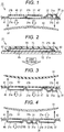
- Fig. 1 is a sectional view illustrating a light-emitting device according to a first embodiment of the present invention.
- a light-emitting device 10 according to this embodiment is illuminating means with a thin-plate shape.
- the light-emitting device 10 is installed on an installation surface 52 of an installation member 51 such as a designed sheet.
- the light-emitting device 10 is attached to the installation surface 52.
- the installation surface 52 is formed as a curved surface.
- the light-emitting device 10 is flexible and can be deformed along the shape of the installation surface 52.
- the light-emitting device 10 includes a plurality of surface-light-emitting units 21.
- the surface-light-emitting unit 21 is provided as light-emitting means extending in the plane shape.
- the light-emitting device 10 is configured to be able to emit light in a wide range because the plurality of surface-light-emitting units 21 is arrayed in the flat plane shape.
- the surface-light-emitting unit 21 includes a light-emitting surface 21a and a non-light-emitting surface 21b.
- the surface-light-emitting unit 21 emits light from the light-emitting surface 21a.
- the non-light-emitting surface 21b is disposed on the back side of the light-emitting surface 21a.
- the light-emitting surface 21a and the non-light-emitting surface 21b have the flat plane shape, and their shapes are parallel to each other.
- Fig. 2 is a sectional view illustrating the surface-light-emitting unit in Fig. 1 .
- the surface-light-emitting unit 21 includes the organic EL, and is formed to be flexible and bendable as a whole.
- the surface-light-emitting unit 21 may be configured by a light-emitting diode (LED) and a diffuser plate, or may alternatively be configured by a cold cathode tube or the like.
- LED light-emitting diode
- diffuser plate or may alternatively be configured by a cold cathode tube or the like.
- the surface-light-emitting unit 21 includes a transparent substrate 72, an anode (anode) 65, an organic layer 73, a cathode (cathode) 64, a sealing member 71, and an insulating layer 66.
- the transparent substrate 72 is disposed on the light-emitting surface 21a side of the surface-light-emitting unit 21.
- the anode 65, the organic layer 73, and the cathode 64 are sequentially stacked on the transparent substrate 72.
- the sealing member 71 is provided to cover a stack of the anode 65, the organic layer 73, and the cathode 64.
- the transparent substrate 72 is formed using a flexible transparent member.
- the material is, for example, a light-transmitting film substrate of polyethylene terephthalate (PET), polycarbonate (PC), or the like.
- the light-transmitting film substrate may alternatively be formed of polyimide, polyethylene naphthalate (PEN), polystyrene (PS), polyether sulfone (PES), polypropylene (PP), or the like.
- PEN polyethylene naphthalate
- PS polystyrene
- PS polyether sulfone
- PP polypropylene
- the anode 65 is a conductive film with transparency.
- the anode 65 is formed by depositing ITO (Indium Tin Oxide: indium tin oxide) or the like as a film on the transparent substrate 72 by a sputtering method or the like.
- the anode 65 may be formed using polyethylenedioxythiophene (PEDOT).
- the organic layer 73 can generate light (visible light) when electric power is supplied.
- the organic layer 73 may be formed of a single light-emitting layer or may be formed by sequentially stacking a hole transport layer, a light-emitting layer, a hole block layer, an electron transport layer, and the like.
- the cathode 64 is formed of, for example, aluminum (Al).
- the cathode 64 is formed to cover the organic layer 73 by a vacuum deposition method or the like.
- a mask is preferably used in the vacuum deposition.
- the cathode 64 may alternatively be formed of lithium fluoride (LiF), a stack of Al and Ca, a stack of Al and LiF, a stack of Al and Ba, or the like.
- an insulating layer 66 is provided between the cathode 64 and the anode 65.
- the insulating layer 66 is formed by, for example, deposing SiO 2 or the like as a film by a sputtering method and then performing the pattern formation as desired by a photolithography method or the like so as to cover the area where the anode 65 and the cathode 64 are to be insulated from each other.
- the sealing member 71 is disposed on the non-light-emitting surface 21b side of the surface-light-emitting unit 21.
- the sealing member 71 is formed of a resin with the insulating property.
- the sealing member 71 is formed to protect the organic layer 73 from moisture or the like.
- the sealing member 71 seals the anode 65, the organic layer 73, and the cathode 64 on the transparent substrate 72. Note that a part of the anode 65 is exposed from the sealing member 71 for the electric connection.
- the sealing member 71 which has the gas barrier property, is formed by overlaying a plurality of layers including an inorganic thin film such as SiO 2 AL 2 O 3 , or SiN x and a soft acrylic resin thin film on a film of PET, PEN, PS, PES, polyimide, or the like.
- an inorganic thin film such as SiO 2 AL 2 O 3 , or SiN x
- a soft acrylic resin thin film on a film of PET, PEN, PS, PES, polyimide, or the like.
- the part of the anode 65 that is exposed from the sealing member 71 constitutes an electrode portion 63 (for anode).
- the electrode portion 63 and the anode 65 are formed of the same material.
- the part of the cathode 64 that is exposed from the sealing member 71 constitutes an electrode portion 62 (for cathode).
- the electrode portion 62 and the cathode 64 are formed of the same material.
- wires (not shown) are attached using solder or silver paste.
- a resin agent may be applied in order to maintain the water resistance and the weather resistance.
- the surface-light-emitting unit 21 is electrically connected through the wire to a power source 32 to be described below.
- the electric power is supplied from the power source 32 through the wires (not shown), the electrode portions 63 and 62, the anode 65, and the cathode 64.
- the light generated in the organic layer 73 by the power supply goes through the anode 65 and the transparent substrate 72 and is extracted from the light-emitting surface 21a to the outside.
- the light-emitting device 10 further includes a substrate 31, and the power source 32 mounted on the substrate 31.
- the substrate 31 includes a flexible wired substrate and has flexibility.
- the substrate 31 and the power source 32 constitute a power source circuit unit 30 for supplying the electric power to the surface-light-emitting unit 21.
- the substrate 31 may alternatively be formed using a hard wired substrate.
- the substrate 31 has a mounting surface 31a and a non-mounting surface 31b.
- the power source 32 is mounted on the mounting surface 31a.
- the non-mounting surface 31b is disposed on the back side of the mounting surface 31a.
- the power source 32 is provided to protrude from the mounting surface 31a.
- the power source circuit unit 30 is arrayed in the plane shape with the plurality of surface-light-emitting units 21. In other words, in the plan view of the light-emitting device 10 with the thin-plate shape, the power source circuit unit 30 does not overlap with the plurality of surface-light-emitting units 21.
- the power source circuit unit 30 is provided beside the surface-light-emitting unit 21.
- the power source circuit unit 30 is provided so that the non-mounting surface 31b is flush with one of the light-emitting surface 21a and the non-light-emitting surface 21b of the surface-light-emitting unit 21.
- the power source circuit unit 30 is provided so that the non-mounting surface 31b is flush with the light-emitting surface 21a of the surface-light-emitting unit 21.
- the power source 32 is mounted on the mounting surface 31a, which is on the side opposite to the light-emitting surface 21a of the surface-light-emitting unit 21.
- the substrate 31 is the substrate for the power source circuit in this embodiment; however, the substrate 31 may be a light emission control substrate for controlling the lighting, the blinking, the emission color, the luminance, or the like of the surface-light-emitting unit 21, or a signal communication substrate for communicating with the outside.
- the power source 32 Since the power source 32 generates heat, a metal sheet with heat conductivity may be placed on the non-mounting surface 31b side of the substrate 31.
- the power source circuit unit 30 is provided so that the surface of the metal sheet is flush with the light-emitting surface 21a of the surface-light-emitting unit 21.
- the light-emitting device 10 further includes a holding sheet 41 and a sealing sheet 46.
- Each of the holding sheet 41 and the sealing sheet 46 is formed using a single flexible sheet material.
- the holding sheet 41 and the sealing sheet 46 are formed of the resin sheet material. Examples of the material include polyethylene terephthalate (PET), polycarbonate (PC), polyimide, polyethylene naphthalate (PEN), polystyrene (PS), polyether sulfone (PES), and polypropylene (PP).
- At least the holding sheet 41 has the light-transmitting property.
- the holding sheet 41 and the sealing sheet 46 overlap with each other in the state that the plurality of surface-light-emitting units 21 and the power source circuit unit 30 are held between the holding sheet 41 and the sealing sheet 46.
- the holding sheet 41 and the sealing sheet 46 are bonded using an OCA film (Optical Clear Adhesive Film), a transparent adhesive, or the like.
- the holding sheet 41 is provided to face the non-mounting surface 31b of the substrate 31 and the light-emitting surface 21a of the surface-light-emitting unit 21 provided to be flush with the non-mounting surface 31b.
- the power source circuit unit 30 and the surface-light-emitting units 21 are held by the holding sheet 41 in the state that the non-mounting surface 31b and the light-emitting surface 21a are in surface contact with the holding sheet 41.
- the sealing sheet 46 is disposed on the side opposite to the holding sheet 41 with respect to the plurality of surface-light-emitting units 21 and the power source circuit unit 30.
- the sealing sheet 46 is provided to integrally cover the plurality of surface-light-emitting units 21 and the power source circuit unit 30 from the side of the non-light-emitting surface 21b and the mounting surface 31a.
- the sealing sheet 46 together with the holding sheet 41 seal the plurality of surface-light-emitting units 21 and the power source circuit unit 30.
- the structure in which the surface-light-emitting units 21 and the power source circuit unit 30 are sealed between the holding sheet 41 and the sealing sheet 46 eliminates the necessity of providing a component for individually supporting the surface-light-emitting unit 21. Therefore, the surface-light-emitting units 21 and the power source circuit unit 30 can be held stably while the light-emitting device 10 is reduced in thickness.
- the light-emitting device 10 is installed on the installation member 51 so that, of the holding sheet 41 and the sealing sheet 46, the holding sheet 41 comes to the installation surface 52 side.
- the light-emitting device 10 is installed on the installation member 51 so that a surface 42 of the holding sheet 41 is in surface contact with the installation surface 52.
- the surface-light-emitting units 21 emit light toward the installation member 51 through the holding sheet 41.
- the light-emitting surface 21a of the surface-light-emitting unit 21 is provided to be flush with the non-mounting surface 31b of the substrate 31 where the power source 32 is not mounted.
- the holding sheet 41 is provided to face these surfaces.
- the holding sheet 41 does not have the unevenness, which would be caused by the power source 32, and can have the flat surface shape.
- a surface 47 of the sealing sheet 46 has the unevenness due to the power source 32.
- the light-emitting device 10 is installed so that the holding sheet 41 with the flat surface shape comes to the installation surface 52 side. This will prevent the space from being formed between the light-emitting device 10 and the installation surface 52, and the thin light-emitting device 10 where the surface-light-emitting unit 21 and the power source circuit unit 30 are sealed can be installed stably.
- the light-emitting device 10 is installed on the installation surface 52.
- the light-emitting device 10 includes the surface-light-emitting units 21, the substrate 31 as a base member, the holding sheet 41 as a first sheet, and the sealing sheet 46 as a second sheet.
- the surface-light-emitting unit 21 has the light-emitting surface 21a and the non-light-emitting surface 21b disposed on the back side of the light-emitting surface 21a, and emits light from the light-emitting surface 21a.
- the substrate 31 has the mounting surface 31a as a first surface, and the non-mounting surface 31b as a second surface, which is disposed on the back side of the mounting surface 31a and provided to be flush with the light-emitting surface 21a as one of the light-emitting surface 21a and the non-light-emitting surface 21b.
- the power source 32 corresponding to the electronic component is mounted on the mounting surface 31a.
- the holding sheet 41 is provided to face the non-mounting surface 31b and the light-emitting surface 21a as one of the light-emitting surface 21a and the non-light-emitting surface 21b provided to be flush with the non-mounting surface 31b.
- the sealing sheet 46 is disposed on the side opposite to the holding sheet 41 with respect to the surface-light-emitting units 21 and the substrate 31, and covers the surface-light-emitting units 21 and the power source 32.
- the light-emitting device 10 is provided so that the holding sheet 41 comes to the installation surface 52 side.
- the light-emitting device 10 with the above structure according to the first embodiment of the present invention includes the holding sheet 41 with the flat surface shape not having the unevenness on the installation surface 52 side.
- the light-emitting device 10 can be stably installed on the installation surface 52.
- the surface-light-emitting unit 21, the substrate 31, the holding sheet 41, and the sealing sheet 46 have the flexibility. Therefore, even if the installation surface 52 is formed as the curved surface, the light-emitting device 10 can be installed easily because the light-emitting device 10 is deformed along the curved shape of the installation surface 52.
- the installation surface 52 where the light-emitting device 10 is installed is not limited to the curved surface but may have a flat plane shape.
- the holding sheet 41 and the like may be formed of the sheet material without the flexibility.
- Fig. 3 is a sectional view illustrating a light-emitting device according to a second embodiment of the present invention.
- the light-emitting device according to this embodiment has the structure basically similar to that of the light-emitting device 10 according to the first embodiment. The description on the overlapping structure will not be repeated.
- the power source circuit unit 30 is provided so that the non-mounting surface 31b is flush with the non-light-emitting surface 21b of the surface-light-emitting unit 21 in this embodiment.
- the holding sheet 41 is provided to face the non-mounting surface 31b of the substrate 31 and the non-light-emitting surface 21b of the surface-light-emitting unit 21 provided to be flush with the non-mounting surface 31b.
- the sealing sheet 46 is provided to cover the plurality of surface-light-emitting units 21 and the power source circuit unit 30 from the side of the light-emitting surface 21a and the mounting surface 31a.
- the light-emitting device is installed on the installation member 51 so that, of the holding sheet 41 and the sealing sheet 46, the holding sheet 41 comes to the installation surface 52 side. Of the holding sheet 41 and the sealing sheet 46, at least the sealing sheet 46 has the light-transmitting property.
- the surface-light-emitting unit 21 emits light toward the space opposite to the installation member 51 through the sealing sheet 46.
- the light-emitting device with the above structure according to the second embodiment of the present invention produces the effect similar to the effect described in the first embodiment.
- Fig. 4 is a sectional view illustrating a light-emitting device according to a third embodiment of the present invention.
- the light-emitting device according to this embodiment has the structure basically similar to that of the light-emitting device 10 according to the first embodiment. The description on the overlapping structure will not be repeated.
- the light-emitting device includes a surface-light-emitting unit 21A and a surface-light-emitting unit 21B as the plurality of surface-light-emitting units 21.
- the power source circuit unit 30 is provided so that the non-mounting surface 31b is flush with the light-emitting surface 21a of the surface-light-emitting unit 21A and the non-light-emitting surface 21b of the surface-light-emitting unit 21B.
- the holding sheet 41 is provided to face the non-mounting surface 31b of the substrate 31 and the light-emitting surface 21a of the surface-light-emitting unit 21A and the non-light-emitting surface 21b of the surface-light-emitting unit 21B, which are provided to be flush with the non-mounting surface 31b.
- the sealing sheet 46 is provided to cover the surface-light-emitting unit 21A, the surface-light-emitting unit 21B, and the power source circuit unit 30 from the side of the light-emitting surface 21b of the surface-light-emitting unit 21A, the light-emitting surface 21a of the surface-light-emitting unit 21B, and the mounting surface 31a of the substrate 31.
- the light-emitting device is installed on the installation member 51 so that, of the holding sheet 41 and the sealing sheet 46, the holding sheet 41 comes to the installation surface 52 side. Both the holding sheet 41 and the sealing sheet 46 have the light-transmitting property.
- the surface-light-emitting unit 21A emits light toward the installation member 51 through the holding sheet 41 and the surface-light-emitting unit 21B emits light toward the space opposite to the installation member 51 through the sealing sheet 46.
- the light-emitting device with the above structure according to the third embodiment of the present invention produces the effect similar to the effect described in the first embodiment.
- Fig. 5 is a sectional view illustrating a light-emitting device according to a fourth embodiment of the present invention.
- the light-emitting device according to this embodiment has the structure basically similar to that of the light-emitting device 10 according to the first embodiment. The description on the overlapping structure will not be repeated.
- the light-emitting device includes a surface-light-emitting unit 26 in addition to the surface-light-emitting units 21 described in the first embodiment.
- the surface-light-emitting unit 26 has the same structure as the surface-light-emitting unit 21, and includes a light-emitting surface 26a and a non-light-emitting surface 26b corresponding to the light-emitting surface 21a and the non-light-emitting surface 21b, respectively.
- the power source circuit unit 30 is provided so that the non-mounting surface 31b is flush with the light-emitting surface 21a of the surface-light-emitting unit 21.
- the surface-light-emitting unit 26 is stacked on the surface-light-emitting unit 21.
- the direction where the surface-light-emitting unit 21 and the surface-light-emitting unit 26 are stacked is the same as the direction where the holding sheet 41 and the sealing sheet 46 are stacked on each other.
- the surface-light-emitting unit 26 is stacked on the surface-light-emitting unit 21 so that the non-light-emitting surface 26b of the surface-light-emitting unit 26 faces the non-light-emitting surface 21b of the surface-light-emitting unit 21.
- the holding sheet 41 is provided to face the non-mounting surface 31b of the substrate 31 and the light-emitting surface 21a of the surface-light-emitting unit 21 provided to be flush with the non-mounting surface 31b.
- the sealing sheet 46 is provided to cover the surface-light-emitting unit 21, the surface-light-emitting unit 26, and the power source circuit unit 30 from the side of the light-emitting surface 26a of the surface-light-emitting unit 26 and the mounting surface 31a of the substrate 31.
- the light-emitting device is installed on the installation member 51 so that, of the holding sheet 41 and the sealing sheet 46, the holding sheet 41 comes to the installation surface 52 side. Both the holding sheet 41 and the sealing sheet 46 have the light-transmitting property.
- the surface-light-emitting unit 21 emits light toward the installation member 51 through the holding sheet 41 and the surface-light-emitting unit 26 emits light toward the space opposite to the installation member 51 through the sealing sheet 46.
- the light-emitting device with the above structure according to the fourth embodiment of the present invention produces the effect similar to the effect described in the first embodiment.
- the light-emitting device is the light-emitting device to be installed on the installation surface.
- the light-emitting device includes the surface-light-emitting unit, the base member, the first sheet, and the second sheet.
- the surface-light-emitting unit has the light-emitting surface and the non-light-emitting surface disposed on the back side of the light-emitting surface, and emits light from the light-emitting surface.
- the base member has a first surface and a second surface which is disposed on a back side of the first surface and which is flush with one of the light-emitting surface and the non-light-emitting surface.
- the base member has the electronic component mounted on the first surface.
- the first sheet is provided to face the second surface and one of the light-emitting surface and the non-light-emitting surface provided to be flush with the second surface.
- the second sheet is disposed on the side opposite to the first sheet with respect to the surface-light-emitting unit and the base member, and covers the surface-light-emitting units and the electronic component.
- the light-emitting device is installed so that the first sheet comes to the installation surface side.
- the first sheet is provided to face the second surface, which is disposed on the back side of the first surface to be provided with the electronic component, and one of the light-emitting surface and the non-light-emitting surface provided to be flush with the second surface. Therefore, the first sheet will not have the unevenness which would be caused by the electronic component. Since the light-emitting device is installed so that the first sheet comes to the installation surface side, the light-emitting device can be stably installed on the installation surface.
- the first sheet and the second sheet have the flexibility.
- the first sheet and the second sheet can be deformed easily along the shape of the installation surface.
- the light-emitting device can be installed on the installation surface more stably.
- the surface-light-emitting unit and the base member have the flexibility.
- the surface-light-emitting unit and the base member can be deformed easily along the shape of the installation surface.
- the light-emitting device can be installed on the installation surface more stably.
- the electronic component includes at least one of the power source for supplying electric power to the surface-light-emitting unit, the control component for controlling the light emission of the surface-light-emitting unit, and the communication component used for the external communication.
- the generation of the space between the light-emitting device and the installation surface which is caused by the unevenness due to the electronic components can be prevented.
- the plurality of surface-light-emitting units is arrayed in the flat plane shape between the first sheet and the second sheet.
- the light-emitting device with the structure in which the plurality of surface-light-emitting units is arrayed in the flat plane shape can be installed stably on the installation surface.
- the plurality of surface-light-emitting units includes a first surface-light-emitting unit whose light-emitting surface is flush with the second surface, and a second surface-light-emitting unit whose non-light-emitting surface is flush with the second surface.
- the light-emitting device with the structure as above which can emit light from both sides, can be installed stably on the installation surface.
- the surface-light-emitting unit is provided so that the light-emitting surface is flush with the second surface.
- the light-emitting device further includes another surface-light-emitting unit.
- This surface-light-emitting unit has a light-emitting surface and a non-light-emitting surface disposed on the back side of the light-emitting surface, emits light from the light-emitting surface, and is stacked on the surface-light-emitting unit so that the non-light-emitting surfaces thereof face each other.
- the light-emitting device with the structure as above which can emit light from both sides, can be installed stably on the installation surface.
- the present invention is mainly applicable to the illuminating apparatus with the thin-plate shape.
Landscapes
- Engineering & Computer Science (AREA)
- General Engineering & Computer Science (AREA)
- Electroluminescent Light Sources (AREA)
- Fastening Of Light Sources Or Lamp Holders (AREA)
- Planar Illumination Modules (AREA)
- Arrangement Of Elements, Cooling, Sealing, Or The Like Of Lighting Devices (AREA)
- Non-Portable Lighting Devices Or Systems Thereof (AREA)
Abstract
Description
- The present invention generally relates to a light-emitting device, more particularly to a light-emitting device installed on an installation surface.
- In regard to conventional light-emitting devices, for example,
JP 2007-149465 A - The luminaire according to Patent Literature 1 includes: the light-emitting panel including the organic EL element; the lighting device that supplies a driving voltage to the light-emitting panel; and the luminaire main body that holds the light-emitting panel and the lighting device. The luminaire main body includes the housing to house the lighting device. The housing is disposed aside with respect to the light-emitting surface of the light-emitting panel, and the light-emitting surface of the light-emitting panel and the front surface of the housing are made almost flush.
- Patent Literature 1:
JP 2007-149465 A - Patent Literature 1 has disclosed the light-emitting device including the surface-light-emitting unit such as the organic EL. Such a light-emitting device is provided with an electronic component, for example a power source for supplying electric power to the surface-light-emitting unit, a control component for controlling the light emission of the surface-light-emitting unit, or a communication component used for external communication.
- Here, it is assumed that the light-emitting device is installed by being attached to an installation surface such as a designed sheet. In this case, the electronic component causes the unevenness and a space may be formed between the light-emitting device and the installation surface. This results in a problem that the light-emitting device cannot be installed stably on the installation surface.
- In view of the above, it is an object of the present invention to solve the above problem and to provide a light-emitting device that can be stably installed on the installation surface.
- A light-emitting device according to one aspect of the present invention is a light-emitting device to be installed on an installation surface. The light-emitting device includes a surface-light-emitting unit, a base member, a first sheet, and a second sheet. The surface-light-emitting unit has a light-emitting surface and a non-light-emitting surface which is disposed on the back side of the light-emitting surface, and emits light from the light-emitting surface. The base member has a first surface and a second surface which is disposed on the back side of the first surface and which is provided to be flush with one of the light-emitting surface and the non-light-emitting surface, and has an electronic component mounted on the first surface. The first sheet is provided to face the second surface and one of the light-emitting surface and the non-light-emitting surface provided to be flush with the second surface. The second sheet is disposed on the side opposite to the first sheet with respect to the surface-light-emitting unit and the base member, and provided to cover the surface-light-emitting unit and the electronic component. The light-emitting device is disposed so that the first sheet comes to the installation surface side.
- According to the present invention, a light-emitting device that can be stably installed on an installation surface can be provided.
-
-
Fig. 1 is a sectional view illustrating a light-emitting device according to a first embodiment of the present invention. -
Fig. 2 is a sectional view illustrating a surface-light-emitting unit inFig. 1 . -
Fig. 3 is a sectional view illustrating a light-emitting device according to a second embodiment of the present invention. -
Fig. 4 is a sectional view illustrating a light-emitting device according to a third embodiment of the present invention. -
Fig. 5 is a sectional view illustrating a light-emitting device according to a fourth embodiment of the present invention. - Embodiments of the present invention will be described with reference to the drawings. Throughout the drawings, the same or corresponding components are denoted by the same reference sign.
-
Fig. 1 is a sectional view illustrating a light-emitting device according to a first embodiment of the present invention. InFig. 1 , a light-emitting device 10 according to this embodiment is illuminating means with a thin-plate shape. The light-emitting device 10 is installed on aninstallation surface 52 of aninstallation member 51 such as a designed sheet. The light-emitting device 10 is attached to theinstallation surface 52. - In this embodiment, the
installation surface 52 is formed as a curved surface. The light-emitting device 10 is flexible and can be deformed along the shape of theinstallation surface 52. - The light-
emitting device 10 includes a plurality of surface-light-emitting units 21. The surface-light-emittingunit 21 is provided as light-emitting means extending in the plane shape. The light-emittingdevice 10 is configured to be able to emit light in a wide range because the plurality of surface-light-emittingunits 21 is arrayed in the flat plane shape. - The surface-light-emitting
unit 21 includes a light-emittingsurface 21a and a non-light-emittingsurface 21b. The surface-light-emittingunit 21 emits light from the light-emittingsurface 21a. The non-light-emittingsurface 21b is disposed on the back side of the light-emittingsurface 21a. The light-emittingsurface 21a and the non-light-emittingsurface 21b have the flat plane shape, and their shapes are parallel to each other. -
Fig. 2 is a sectional view illustrating the surface-light-emitting unit inFig. 1 . InFig. 2 , in this embodiment, the surface-light-emittingunit 21 includes the organic EL, and is formed to be flexible and bendable as a whole. The surface-light-emittingunit 21 may be configured by a light-emitting diode (LED) and a diffuser plate, or may alternatively be configured by a cold cathode tube or the like. - The surface-light-
emitting unit 21 includes atransparent substrate 72, an anode (anode) 65, an organic layer 73, a cathode (cathode) 64, a sealingmember 71, and aninsulating layer 66. - The
transparent substrate 72 is disposed on the light-emittingsurface 21a side of the surface-light-emitting unit 21. Theanode 65, the organic layer 73, and the cathode 64 are sequentially stacked on thetransparent substrate 72. The sealingmember 71 is provided to cover a stack of theanode 65, the organic layer 73, and the cathode 64. - The
transparent substrate 72 is formed using a flexible transparent member. The material is, for example, a light-transmitting film substrate of polyethylene terephthalate (PET), polycarbonate (PC), or the like. - The light-transmitting film substrate may alternatively be formed of polyimide, polyethylene naphthalate (PEN), polystyrene (PS), polyether sulfone (PES), polypropylene (PP), or the like.
- The
anode 65 is a conductive film with transparency. Theanode 65 is formed by depositing ITO (Indium Tin Oxide: indium tin oxide) or the like as a film on thetransparent substrate 72 by a sputtering method or the like. Alternatively, theanode 65 may be formed using polyethylenedioxythiophene (PEDOT). - The organic layer 73 can generate light (visible light) when electric power is supplied. The organic layer 73 may be formed of a single light-emitting layer or may be formed by sequentially stacking a hole transport layer, a light-emitting layer, a hole block layer, an electron transport layer, and the like.
- The cathode 64 is formed of, for example, aluminum (Al). The cathode 64 is formed to cover the organic layer 73 by a vacuum deposition method or the like. For patterning the cathode 64 in a predetermined shape, a mask is preferably used in the vacuum deposition. The cathode 64 may alternatively be formed of lithium fluoride (LiF), a stack of Al and Ca, a stack of Al and LiF, a stack of Al and Ba, or the like.
- To prevent the short-circuiting between the cathode 64 and the
anode 65, an insulatinglayer 66 is provided between the cathode 64 and theanode 65. The insulatinglayer 66 is formed by, for example, deposing SiO2 or the like as a film by a sputtering method and then performing the pattern formation as desired by a photolithography method or the like so as to cover the area where theanode 65 and the cathode 64 are to be insulated from each other. - The sealing
member 71 is disposed on the non-light-emittingsurface 21b side of the surface-light-emittingunit 21. The sealingmember 71 is formed of a resin with the insulating property. The sealingmember 71 is formed to protect the organic layer 73 from moisture or the like. The sealingmember 71 seals theanode 65, the organic layer 73, and the cathode 64 on thetransparent substrate 72. Note that a part of theanode 65 is exposed from the sealingmember 71 for the electric connection. - The sealing
member 71, which has the gas barrier property, is formed by overlaying a plurality of layers including an inorganic thin film such as SiO2 AL2O3, or SiNx and a soft acrylic resin thin film on a film of PET, PEN, PS, PES, polyimide, or the like. - The part of the
anode 65 that is exposed from the sealing member 71 (the right part inFig. 2 ) constitutes an electrode portion 63 (for anode). Theelectrode portion 63 and theanode 65 are formed of the same material. The part of the cathode 64 that is exposed from the sealing member 71 (the left part inFig. 2 ) constitutes an electrode portion 62 (for cathode). Theelectrode portion 62 and the cathode 64 are formed of the same material. To theelectrode portion 63 and theelectrode portion 62, wires (not shown) are attached using solder or silver paste. On the portion where the wires are attached, a resin agent may be applied in order to maintain the water resistance and the weather resistance. The surface-light-emittingunit 21 is electrically connected through the wire to apower source 32 to be described below. - To the organic layer 73 of the surface-light-emitting
unit 21, the electric power is supplied from thepower source 32 through the wires (not shown), theelectrode portions anode 65, and the cathode 64. The light generated in the organic layer 73 by the power supply goes through theanode 65 and thetransparent substrate 72 and is extracted from the light-emittingsurface 21a to the outside. - In
Fig. 1 , the light-emittingdevice 10 further includes asubstrate 31, and thepower source 32 mounted on thesubstrate 31. In this embodiment, thesubstrate 31 includes a flexible wired substrate and has flexibility. Thesubstrate 31 and thepower source 32 constitute a powersource circuit unit 30 for supplying the electric power to the surface-light-emittingunit 21. Note that thesubstrate 31 may alternatively be formed using a hard wired substrate. - The
substrate 31 has a mountingsurface 31a and anon-mounting surface 31b. Thepower source 32 is mounted on the mountingsurface 31a. Thenon-mounting surface 31b is disposed on the back side of the mountingsurface 31a. Thepower source 32 is provided to protrude from the mountingsurface 31a. - The power
source circuit unit 30 is arrayed in the plane shape with the plurality of surface-light-emittingunits 21. In other words, in the plan view of the light-emittingdevice 10 with the thin-plate shape, the powersource circuit unit 30 does not overlap with the plurality of surface-light-emittingunits 21. The powersource circuit unit 30 is provided beside the surface-light-emittingunit 21. - The power
source circuit unit 30 is provided so that thenon-mounting surface 31b is flush with one of the light-emittingsurface 21a and the non-light-emittingsurface 21b of the surface-light-emittingunit 21. In this embodiment, the powersource circuit unit 30 is provided so that thenon-mounting surface 31b is flush with the light-emittingsurface 21a of the surface-light-emittingunit 21. With respect to thesubstrate 31, thepower source 32 is mounted on the mountingsurface 31a, which is on the side opposite to the light-emittingsurface 21a of the surface-light-emittingunit 21. - The
substrate 31 is the substrate for the power source circuit in this embodiment; however, thesubstrate 31 may be a light emission control substrate for controlling the lighting, the blinking, the emission color, the luminance, or the like of the surface-light-emittingunit 21, or a signal communication substrate for communicating with the outside. - Since the
power source 32 generates heat, a metal sheet with heat conductivity may be placed on thenon-mounting surface 31b side of thesubstrate 31. In this case, the powersource circuit unit 30 is provided so that the surface of the metal sheet is flush with the light-emittingsurface 21a of the surface-light-emittingunit 21. - The light-emitting
device 10 further includes a holdingsheet 41 and a sealingsheet 46. Each of the holdingsheet 41 and the sealingsheet 46 is formed using a single flexible sheet material. The holdingsheet 41 and the sealingsheet 46 are formed of the resin sheet material. Examples of the material include polyethylene terephthalate (PET), polycarbonate (PC), polyimide, polyethylene naphthalate (PEN), polystyrene (PS), polyether sulfone (PES), and polypropylene (PP). - In this embodiment, of the holding
sheet 41 and the sealingsheet 46, at least the holdingsheet 41 has the light-transmitting property. - The holding
sheet 41 and the sealingsheet 46 overlap with each other in the state that the plurality of surface-light-emittingunits 21 and the powersource circuit unit 30 are held between the holdingsheet 41 and the sealingsheet 46. The holdingsheet 41 and the sealingsheet 46 are bonded using an OCA film (Optical Clear Adhesive Film), a transparent adhesive, or the like. - The holding
sheet 41 is provided to face thenon-mounting surface 31b of thesubstrate 31 and the light-emittingsurface 21a of the surface-light-emittingunit 21 provided to be flush with thenon-mounting surface 31b. The powersource circuit unit 30 and the surface-light-emittingunits 21 are held by the holdingsheet 41 in the state that thenon-mounting surface 31b and the light-emittingsurface 21a are in surface contact with the holdingsheet 41. - The sealing
sheet 46 is disposed on the side opposite to the holdingsheet 41 with respect to the plurality of surface-light-emittingunits 21 and the powersource circuit unit 30. The sealingsheet 46 is provided to integrally cover the plurality of surface-light-emittingunits 21 and the powersource circuit unit 30 from the side of the non-light-emittingsurface 21b and the mountingsurface 31a. The sealingsheet 46 together with the holdingsheet 41 seal the plurality of surface-light-emittingunits 21 and the powersource circuit unit 30. - The structure in which the surface-light-emitting
units 21 and the powersource circuit unit 30 are sealed between the holdingsheet 41 and the sealingsheet 46 eliminates the necessity of providing a component for individually supporting the surface-light-emittingunit 21. Therefore, the surface-light-emittingunits 21 and the powersource circuit unit 30 can be held stably while the light-emittingdevice 10 is reduced in thickness. - The light-emitting
device 10 is installed on theinstallation member 51 so that, of the holdingsheet 41 and the sealingsheet 46, the holdingsheet 41 comes to theinstallation surface 52 side. The light-emittingdevice 10 is installed on theinstallation member 51 so that asurface 42 of the holdingsheet 41 is in surface contact with theinstallation surface 52. The surface-light-emittingunits 21 emit light toward theinstallation member 51 through the holdingsheet 41. - In this embodiment, the light-emitting
surface 21a of the surface-light-emittingunit 21 is provided to be flush with thenon-mounting surface 31b of thesubstrate 31 where thepower source 32 is not mounted. The holdingsheet 41 is provided to face these surfaces. - With this structure, the holding
sheet 41 does not have the unevenness, which would be caused by thepower source 32, and can have the flat surface shape. On the other hand, asurface 47 of the sealingsheet 46 has the unevenness due to thepower source 32. In view of this, the light-emittingdevice 10 is installed so that the holdingsheet 41 with the flat surface shape comes to theinstallation surface 52 side. This will prevent the space from being formed between the light-emittingdevice 10 and theinstallation surface 52, and the thin light-emittingdevice 10 where the surface-light-emittingunit 21 and the powersource circuit unit 30 are sealed can be installed stably. - Description is made of the summary of the above structure of the light-emitting
device 10 according to the first embodiment of the present invention. The light-emittingdevice 10 according to this embodiment is installed on theinstallation surface 52. The light-emittingdevice 10 includes the surface-light-emittingunits 21, thesubstrate 31 as a base member, the holdingsheet 41 as a first sheet, and the sealingsheet 46 as a second sheet. The surface-light-emittingunit 21 has the light-emittingsurface 21a and the non-light-emittingsurface 21b disposed on the back side of the light-emittingsurface 21a, and emits light from the light-emittingsurface 21a. Thesubstrate 31 has the mountingsurface 31a as a first surface, and thenon-mounting surface 31b as a second surface, which is disposed on the back side of the mountingsurface 31a and provided to be flush with the light-emittingsurface 21a as one of the light-emittingsurface 21a and the non-light-emittingsurface 21b. On the mountingsurface 31a, thepower source 32 corresponding to the electronic component is mounted. The holdingsheet 41 is provided to face thenon-mounting surface 31b and the light-emittingsurface 21a as one of the light-emittingsurface 21a and the non-light-emittingsurface 21b provided to be flush with thenon-mounting surface 31b. The sealingsheet 46 is disposed on the side opposite to the holdingsheet 41 with respect to the surface-light-emittingunits 21 and thesubstrate 31, and covers the surface-light-emittingunits 21 and thepower source 32. The light-emittingdevice 10 is provided so that the holdingsheet 41 comes to theinstallation surface 52 side. - The light-emitting
device 10 with the above structure according to the first embodiment of the present invention includes the holdingsheet 41 with the flat surface shape not having the unevenness on theinstallation surface 52 side. Thus, the light-emittingdevice 10 can be stably installed on theinstallation surface 52. In this embodiment, the surface-light-emittingunit 21, thesubstrate 31, the holdingsheet 41, and the sealingsheet 46 have the flexibility. Therefore, even if theinstallation surface 52 is formed as the curved surface, the light-emittingdevice 10 can be installed easily because the light-emittingdevice 10 is deformed along the curved shape of theinstallation surface 52. - Note that the
installation surface 52 where the light-emittingdevice 10 is installed is not limited to the curved surface but may have a flat plane shape. In this case, the holdingsheet 41 and the like may be formed of the sheet material without the flexibility. -
Fig. 3 is a sectional view illustrating a light-emitting device according to a second embodiment of the present invention. The light-emitting device according to this embodiment has the structure basically similar to that of the light-emittingdevice 10 according to the first embodiment. The description on the overlapping structure will not be repeated. - In
Fig. 3 , the powersource circuit unit 30 is provided so that thenon-mounting surface 31b is flush with the non-light-emittingsurface 21b of the surface-light-emittingunit 21 in this embodiment. The holdingsheet 41 is provided to face thenon-mounting surface 31b of thesubstrate 31 and the non-light-emittingsurface 21b of the surface-light-emittingunit 21 provided to be flush with thenon-mounting surface 31b. The sealingsheet 46 is provided to cover the plurality of surface-light-emittingunits 21 and the powersource circuit unit 30 from the side of the light-emittingsurface 21a and the mountingsurface 31a. - The light-emitting device according to this embodiment is installed on the
installation member 51 so that, of the holdingsheet 41 and the sealingsheet 46, the holdingsheet 41 comes to theinstallation surface 52 side. Of the holdingsheet 41 and the sealingsheet 46, at least the sealingsheet 46 has the light-transmitting property. The surface-light-emittingunit 21 emits light toward the space opposite to theinstallation member 51 through the sealingsheet 46. - The light-emitting device with the above structure according to the second embodiment of the present invention produces the effect similar to the effect described in the first embodiment.
-
Fig. 4 is a sectional view illustrating a light-emitting device according to a third embodiment of the present invention. The light-emitting device according to this embodiment has the structure basically similar to that of the light-emittingdevice 10 according to the first embodiment. The description on the overlapping structure will not be repeated. - In
Fig. 4 , the light-emitting device according to this embodiment includes a surface-light-emittingunit 21A and a surface-light-emitting unit 21B as the plurality of surface-light-emittingunits 21. - The power
source circuit unit 30 is provided so that thenon-mounting surface 31b is flush with the light-emittingsurface 21a of the surface-light-emittingunit 21A and the non-light-emittingsurface 21b of the surface-light-emitting unit 21B. The holdingsheet 41 is provided to face thenon-mounting surface 31b of thesubstrate 31 and the light-emittingsurface 21a of the surface-light-emittingunit 21A and the non-light-emittingsurface 21b of the surface-light-emitting unit 21B, which are provided to be flush with thenon-mounting surface 31b. The sealingsheet 46 is provided to cover the surface-light-emittingunit 21A, the surface-light-emitting unit 21B, and the powersource circuit unit 30 from the side of the light-emittingsurface 21b of the surface-light-emittingunit 21A, the light-emittingsurface 21a of the surface-light-emitting unit 21B, and the mountingsurface 31a of thesubstrate 31. - The light-emitting device according to this embodiment is installed on the
installation member 51 so that, of the holdingsheet 41 and the sealingsheet 46, the holdingsheet 41 comes to theinstallation surface 52 side. Both the holdingsheet 41 and the sealingsheet 46 have the light-transmitting property. The surface-light-emittingunit 21A emits light toward theinstallation member 51 through the holdingsheet 41 and the surface-light-emitting unit 21B emits light toward the space opposite to theinstallation member 51 through the sealingsheet 46. - The light-emitting device with the above structure according to the third embodiment of the present invention produces the effect similar to the effect described in the first embodiment.
-
Fig. 5 is a sectional view illustrating a light-emitting device according to a fourth embodiment of the present invention. The light-emitting device according to this embodiment has the structure basically similar to that of the light-emittingdevice 10 according to the first embodiment. The description on the overlapping structure will not be repeated. - In
Fig. 5 , the light-emitting device according to this embodiment includes a surface-light-emittingunit 26 in addition to the surface-light-emittingunits 21 described in the first embodiment. The surface-light-emittingunit 26 has the same structure as the surface-light-emittingunit 21, and includes a light-emitting surface 26a and a non-light-emitting surface 26b corresponding to the light-emittingsurface 21a and the non-light-emittingsurface 21b, respectively. - The power
source circuit unit 30 is provided so that thenon-mounting surface 31b is flush with the light-emittingsurface 21a of the surface-light-emittingunit 21. The surface-light-emittingunit 26 is stacked on the surface-light-emittingunit 21. The direction where the surface-light-emittingunit 21 and the surface-light-emittingunit 26 are stacked is the same as the direction where the holdingsheet 41 and the sealingsheet 46 are stacked on each other. The surface-light-emittingunit 26 is stacked on the surface-light-emittingunit 21 so that the non-light-emitting surface 26b of the surface-light-emittingunit 26 faces the non-light-emittingsurface 21b of the surface-light-emittingunit 21. - The holding
sheet 41 is provided to face thenon-mounting surface 31b of thesubstrate 31 and the light-emittingsurface 21a of the surface-light-emittingunit 21 provided to be flush with thenon-mounting surface 31b. The sealingsheet 46 is provided to cover the surface-light-emittingunit 21, the surface-light-emittingunit 26, and the powersource circuit unit 30 from the side of the light-emitting surface 26a of the surface-light-emittingunit 26 and the mountingsurface 31a of thesubstrate 31. - The light-emitting device according to this embodiment is installed on the
installation member 51 so that, of the holdingsheet 41 and the sealingsheet 46, the holdingsheet 41 comes to theinstallation surface 52 side. Both the holdingsheet 41 and the sealingsheet 46 have the light-transmitting property. The surface-light-emittingunit 21 emits light toward theinstallation member 51 through the holdingsheet 41 and the surface-light-emittingunit 26 emits light toward the space opposite to theinstallation member 51 through the sealingsheet 46. - The light-emitting device with the above structure according to the fourth embodiment of the present invention produces the effect similar to the effect described in the first embodiment.
- The light-emitting device according to one aspect of the present invention is the light-emitting device to be installed on the installation surface. The light-emitting device includes the surface-light-emitting unit, the base member, the first sheet, and the second sheet. The surface-light-emitting unit has the light-emitting surface and the non-light-emitting surface disposed on the back side of the light-emitting surface, and emits light from the light-emitting surface. The base member has a first surface and a second surface which is disposed on a back side of the first surface and which is flush with one of the light-emitting surface and the non-light-emitting surface. The base member has the electronic component mounted on the first surface. The first sheet is provided to face the second surface and one of the light-emitting surface and the non-light-emitting surface provided to be flush with the second surface. The second sheet is disposed on the side opposite to the first sheet with respect to the surface-light-emitting unit and the base member, and covers the surface-light-emitting units and the electronic component. The light-emitting device is installed so that the first sheet comes to the installation surface side.
- In the light-emitting device with such a structure, the first sheet is provided to face the second surface, which is disposed on the back side of the first surface to be provided with the electronic component, and one of the light-emitting surface and the non-light-emitting surface provided to be flush with the second surface. Therefore, the first sheet will not have the unevenness which would be caused by the electronic component. Since the light-emitting device is installed so that the first sheet comes to the installation surface side, the light-emitting device can be stably installed on the installation surface.
- It is preferable that the first sheet and the second sheet have the flexibility. In the light-emitting device with such a structure, the first sheet and the second sheet can be deformed easily along the shape of the installation surface. Thus, the light-emitting device can be installed on the installation surface more stably.
- It is preferable that the surface-light-emitting unit and the base member have the flexibility. In the light-emitting device with such a structure, the surface-light-emitting unit and the base member can be deformed easily along the shape of the installation surface. Thus, the light-emitting device can be installed on the installation surface more stably.
- It is preferable that the electronic component includes at least one of the power source for supplying electric power to the surface-light-emitting unit, the control component for controlling the light emission of the surface-light-emitting unit, and the communication component used for the external communication.
- In the light-emitting device with such a structure, the generation of the space between the light-emitting device and the installation surface which is caused by the unevenness due to the electronic components can be prevented.
- It is preferable that the plurality of surface-light-emitting units is arrayed in the flat plane shape between the first sheet and the second sheet.
- The light-emitting device with the structure in which the plurality of surface-light-emitting units is arrayed in the flat plane shape can be installed stably on the installation surface.
- It is preferable that the plurality of surface-light-emitting units includes a first surface-light-emitting unit whose light-emitting surface is flush with the second surface, and a second surface-light-emitting unit whose non-light-emitting surface is flush with the second surface.
- The light-emitting device with the structure as above, which can emit light from both sides, can be installed stably on the installation surface.
- It is preferable that the surface-light-emitting unit is provided so that the light-emitting surface is flush with the second surface. The light-emitting device further includes another surface-light-emitting unit. This surface-light-emitting unit has a light-emitting surface and a non-light-emitting surface disposed on the back side of the light-emitting surface, emits light from the light-emitting surface, and is stacked on the surface-light-emitting unit so that the non-light-emitting surfaces thereof face each other.
- The light-emitting device with the structure as above, which can emit light from both sides, can be installed stably on the installation surface.
- The embodiments disclosed herein are presented for the purposes of illustration and description in all respects and are not intended to limit the subject matter described herein to the precise form disclosed. The scope of the present invention should be presented not by the above description but by the scope of claims, and the meaning equivalent to the scope of claims and all changes that come within the range are intended to be embraced therein.
- The present invention is mainly applicable to the illuminating apparatus with the thin-plate shape.
-
- 10
- Light-emitting device
- 21, 21A, 21B, 26
- Surface-light-emitting unit
- 21a, 26a
- Light-emitting surface
- 21b, 26b
- Non-light-emitting surface
- 30
- Power source circuit unit
- 31
- Substrate
- 31a
- Mounting surface
- 31b
- Non-mounting surface
- 32
- Power source
- 41
- Holding sheet
- 42, 47
- Surface
- 46
- Sealing sheet
- 51
- Installation member
- 52
- Installation surface
- 62, 63
- Electrode portion
- 64
- Cathode
- 65
- Anode
- 66
- Insulating layer
- 71
- Sealing member
- 72
- Transparent substrate
- 73
- Organic layer
Claims (7)
- A light-emitting device to be installed on an installation surface, comprising:a surface-light-emitting unit having a light-emitting surface and a non-light-emitting surface disposed on a back side of the light-emitting surface, and emitting light from the light-emitting surface;a base member having a first surface and a second surface disposed on a back side of the first surface and provided to be flush with one of the light-emitting surface and the non-light-emitting surface, and having an electronic component mounted on the first surface;a first sheet provided to face the second surface and one of the light-emitting surface and the non-light-emitting surface that is provided to be flush with the second surface; anda second sheet disposed on a side opposite to the first sheet with respect to the surface-light-emitting unit and the base member so as to cover the surface-light-emitting unit and the electronic component, wherein the light-emitting device is installed so that the first sheet comes to the installation surface side.
- The light-emitting device according to claim 1, wherein the first sheet and the second sheet have flexibility.
- The light-emitting device according to claim 1 or 2, wherein the surface-light-emitting unit and the base member have flexibility.
- The light-emitting device according to any one of claims 1 to 3, wherein the electronic component includes at least one of a power source for supplying electric power to the surface-light-emitting unit, a control component for controlling light emission of the surface-light-emitting unit, and a communication component used for external communication.
- The light-emitting device according to any one of claims 1 to 4, wherein a plurality of the surface-light-emitting units is arrayed in a plane shape between the first sheet and the second sheet.
- The light-emitting device according to claim 5, wherein the plurality of surface-light-emitting units includes a first surface-light-emitting unit whose light-emitting surface is flush with the second surface and a second surface-light-emitting unit whose non-light-emitting surface is flush with the second surface.
- The light-emitting device according to any one of claims 1 to 6, wherein
the surface-light-emitting unit is provided so that the light-emitting surface is flush with the second surface, and
another surface-light-emitting unit having a light-emitting surface and a non-light-emitting surface disposed on the back side of the light-emitting surface, emitting light from the light-emitting surface, and stacked on the surface-light-emitting unit is provided so that the non-light-emitting surfaces thereof face each other.
Applications Claiming Priority (2)
| Application Number | Priority Date | Filing Date | Title |
|---|---|---|---|
| JP2014187821 | 2014-09-16 | ||
| PCT/JP2015/071444 WO2016042921A1 (en) | 2014-09-16 | 2015-07-29 | Light emitting device |
Publications (2)
| Publication Number | Publication Date |
|---|---|
| EP3196537A1 true EP3196537A1 (en) | 2017-07-26 |
| EP3196537A4 EP3196537A4 (en) | 2018-05-30 |
Family
ID=55532965
Family Applications (1)
| Application Number | Title | Priority Date | Filing Date |
|---|---|---|---|
| EP15841835.0A Withdrawn EP3196537A4 (en) | 2014-09-16 | 2015-07-29 | Light emitting device |
Country Status (4)
| Country | Link |
|---|---|
| US (1) | US10077890B2 (en) |
| EP (1) | EP3196537A4 (en) |
| JP (1) | JP6512225B2 (en) |
| WO (1) | WO2016042921A1 (en) |
Families Citing this family (1)
| Publication number | Priority date | Publication date | Assignee | Title |
|---|---|---|---|---|
| EP3661327A1 (en) * | 2017-07-26 | 2020-06-03 | Light Flex Technology, S.L. | Laminar luminaire and method of manufacture |
Family Cites Families (7)
| Publication number | Priority date | Publication date | Assignee | Title |
|---|---|---|---|---|
| US7733441B2 (en) * | 2004-06-03 | 2010-06-08 | Semiconductor Energy Labortory Co., Ltd. | Organic electroluminescent lighting system provided with an insulating layer containing fluorescent material |
| JP4470870B2 (en) | 2005-11-25 | 2010-06-02 | パナソニック電工株式会社 | lighting equipment |
| US8328375B2 (en) | 2006-09-29 | 2012-12-11 | Osram Opto Semiconductors Gmbh | Organic lighting device and lighting equipment |
| JP5287541B2 (en) * | 2009-06-24 | 2013-09-11 | セイコーエプソン株式会社 | Electro-optical device and electronic apparatus |
| CN102598345B (en) * | 2009-09-11 | 2015-11-25 | 皇家飞利浦电子股份有限公司 | OLED device with protective covering |
| JP5184705B1 (en) * | 2012-01-05 | 2013-04-17 | 日東電工株式会社 | Wireless power feeding type light emitting element and light emitting device |
| JP5895762B2 (en) * | 2012-07-27 | 2016-03-30 | コニカミノルタ株式会社 | Organic electroluminescent device and organic electroluminescent panel sealing method |
-
2015
- 2015-07-29 EP EP15841835.0A patent/EP3196537A4/en not_active Withdrawn
- 2015-07-29 US US15/509,724 patent/US10077890B2/en active Active
- 2015-07-29 JP JP2016548765A patent/JP6512225B2/en active Active
- 2015-07-29 WO PCT/JP2015/071444 patent/WO2016042921A1/en not_active Ceased
Also Published As
| Publication number | Publication date |
|---|---|
| JP6512225B2 (en) | 2019-05-15 |
| EP3196537A4 (en) | 2018-05-30 |
| US10077890B2 (en) | 2018-09-18 |
| US20170299156A1 (en) | 2017-10-19 |
| WO2016042921A1 (en) | 2016-03-24 |
| JPWO2016042921A1 (en) | 2017-06-29 |
Similar Documents
| Publication | Publication Date | Title |
|---|---|---|
| US9196869B2 (en) | Manufacturing method of light-emitting device with nano-imprinting wiring | |
| EP2838317B1 (en) | Organic electroluminescence module and organic electroluminescence module power supply structure | |
| JP5698362B2 (en) | Light source device on printed circuit board and light source device having a plurality of light source devices | |
| CN106576403B (en) | Surface illuminated panel and elastic sheath | |
| CN103189679B (en) | Light emitting module | |
| US10077890B2 (en) | Light-emitting device | |
| US9853239B2 (en) | Surface light-emitting unit | |
| US20180054861A1 (en) | Planar light-emitting module | |
| JP5983894B2 (en) | Surface emitting module | |
| JP6609939B2 (en) | Light emitting device | |
| JP6101458B2 (en) | Organic EL module and laying structure of organic EL module | |
| JP2017062965A (en) | Light emitting device | |
| WO2014027395A1 (en) | Light-emitting device equipped with organic el element | |
| JP2015185241A (en) | Luminescent panel and lighting fixture | |
| JP2011187217A (en) | Organic el module | |
| US20140111084A1 (en) | Oled lighting device | |
| JP5293910B1 (en) | lighting equipment | |
| US9559315B2 (en) | Surface light-emitting element and light-emitting device | |
| JP2016119200A (en) | Light emitting device | |
| CN105720023A (en) | Display and its thermoelectric conduction element | |
| JP2016184538A (en) | Light emitting device | |
| JP2015170574A (en) | Light emitting device and flexible substrate | |
| JP5602483B2 (en) | Light emitting module and lighting apparatus using the module | |
| CN103974484A (en) | Lighting device | |
| JPWO2014175020A1 (en) | Internal illumination system |
Legal Events
| Date | Code | Title | Description |
|---|---|---|---|
| PUAI | Public reference made under article 153(3) epc to a published international application that has entered the european phase |
Free format text: ORIGINAL CODE: 0009012 |
|
| 17P | Request for examination filed |
Effective date: 20170316 |
|
| AK | Designated contracting states |
Kind code of ref document: A1 Designated state(s): AL AT BE BG CH CY CZ DE DK EE ES FI FR GB GR HR HU IE IS IT LI LT LU LV MC MK MT NL NO PL PT RO RS SE SI SK SM TR |
|
| AX | Request for extension of the european patent |
Extension state: BA ME |
|
| DAV | Request for validation of the european patent (deleted) | ||
| DAX | Request for extension of the european patent (deleted) | ||
| A4 | Supplementary search report drawn up and despatched |
Effective date: 20180504 |
|
| RIC1 | Information provided on ipc code assigned before grant |
Ipc: F21V 19/00 20060101ALI20180426BHEP Ipc: F21V 23/00 20150101ALI20180426BHEP Ipc: F21Y 105/00 20160101ALI20180426BHEP Ipc: H05B 33/02 20060101ALI20180426BHEP Ipc: H01L 51/50 20060101ALI20180426BHEP Ipc: F21S 2/00 20160101AFI20180426BHEP Ipc: H05B 33/04 20060101ALI20180426BHEP |
|
| STAA | Information on the status of an ep patent application or granted ep patent |
Free format text: STATUS: THE APPLICATION IS DEEMED TO BE WITHDRAWN |
|
| 18D | Application deemed to be withdrawn |
Effective date: 20200201 |