EP3196018A1 - Substrate bonding method, touch control substrate and display device - Google Patents
Substrate bonding method, touch control substrate and display device Download PDFInfo
- Publication number
- EP3196018A1 EP3196018A1 EP15753302.7A EP15753302A EP3196018A1 EP 3196018 A1 EP3196018 A1 EP 3196018A1 EP 15753302 A EP15753302 A EP 15753302A EP 3196018 A1 EP3196018 A1 EP 3196018A1
- Authority
- EP
- European Patent Office
- Prior art keywords
- substrate
- adhesive
- removed layer
- curable adhesive
- bonding
- Prior art date
- Legal status (The legal status is an assumption and is not a legal conclusion. Google has not performed a legal analysis and makes no representation as to the accuracy of the status listed.)
- Granted
Links
Images

Classifications
-
- B—PERFORMING OPERATIONS; TRANSPORTING
- B32—LAYERED PRODUCTS
- B32B—LAYERED PRODUCTS, i.e. PRODUCTS BUILT-UP OF STRATA OF FLAT OR NON-FLAT, e.g. CELLULAR OR HONEYCOMB, FORM
- B32B37/00—Methods or apparatus for laminating, e.g. by curing or by ultrasonic bonding
- B32B37/12—Methods or apparatus for laminating, e.g. by curing or by ultrasonic bonding characterised by using adhesives
- B32B37/1284—Application of adhesive
-
- B—PERFORMING OPERATIONS; TRANSPORTING
- B32—LAYERED PRODUCTS
- B32B—LAYERED PRODUCTS, i.e. PRODUCTS BUILT-UP OF STRATA OF FLAT OR NON-FLAT, e.g. CELLULAR OR HONEYCOMB, FORM
- B32B37/00—Methods or apparatus for laminating, e.g. by curing or by ultrasonic bonding
- B32B37/12—Methods or apparatus for laminating, e.g. by curing or by ultrasonic bonding characterised by using adhesives
-
- B—PERFORMING OPERATIONS; TRANSPORTING
- B32—LAYERED PRODUCTS
- B32B—LAYERED PRODUCTS, i.e. PRODUCTS BUILT-UP OF STRATA OF FLAT OR NON-FLAT, e.g. CELLULAR OR HONEYCOMB, FORM
- B32B37/00—Methods or apparatus for laminating, e.g. by curing or by ultrasonic bonding
- B32B37/0007—Methods or apparatus for laminating, e.g. by curing or by ultrasonic bonding involving treatment or provisions in order to avoid deformation or air inclusion, e.g. to improve surface quality
- B32B37/003—Methods or apparatus for laminating, e.g. by curing or by ultrasonic bonding involving treatment or provisions in order to avoid deformation or air inclusion, e.g. to improve surface quality to avoid air inclusion
-
- B—PERFORMING OPERATIONS; TRANSPORTING
- B32—LAYERED PRODUCTS
- B32B—LAYERED PRODUCTS, i.e. PRODUCTS BUILT-UP OF STRATA OF FLAT OR NON-FLAT, e.g. CELLULAR OR HONEYCOMB, FORM
- B32B37/00—Methods or apparatus for laminating, e.g. by curing or by ultrasonic bonding
- B32B37/02—Methods or apparatus for laminating, e.g. by curing or by ultrasonic bonding characterised by a sequence of laminating steps, e.g. by adding new layers at consecutive laminating stations
-
- B—PERFORMING OPERATIONS; TRANSPORTING
- B32—LAYERED PRODUCTS
- B32B—LAYERED PRODUCTS, i.e. PRODUCTS BUILT-UP OF STRATA OF FLAT OR NON-FLAT, e.g. CELLULAR OR HONEYCOMB, FORM
- B32B38/00—Ancillary operations in connection with laminating processes
- B32B38/10—Removing layers, or parts of layers, mechanically or chemically
-
- B—PERFORMING OPERATIONS; TRANSPORTING
- B32—LAYERED PRODUCTS
- B32B—LAYERED PRODUCTS, i.e. PRODUCTS BUILT-UP OF STRATA OF FLAT OR NON-FLAT, e.g. CELLULAR OR HONEYCOMB, FORM
- B32B38/00—Ancillary operations in connection with laminating processes
- B32B38/18—Handling of layers or the laminate
-
- G—PHYSICS
- G02—OPTICS
- G02F—OPTICAL DEVICES OR ARRANGEMENTS FOR THE CONTROL OF LIGHT BY MODIFICATION OF THE OPTICAL PROPERTIES OF THE MEDIA OF THE ELEMENTS INVOLVED THEREIN; NON-LINEAR OPTICS; FREQUENCY-CHANGING OF LIGHT; OPTICAL LOGIC ELEMENTS; OPTICAL ANALOGUE/DIGITAL CONVERTERS
- G02F1/00—Devices or arrangements for the control of the intensity, colour, phase, polarisation or direction of light arriving from an independent light source, e.g. switching, gating or modulating; Non-linear optics
- G02F1/01—Devices or arrangements for the control of the intensity, colour, phase, polarisation or direction of light arriving from an independent light source, e.g. switching, gating or modulating; Non-linear optics for the control of the intensity, phase, polarisation or colour
- G02F1/13—Devices or arrangements for the control of the intensity, colour, phase, polarisation or direction of light arriving from an independent light source, e.g. switching, gating or modulating; Non-linear optics for the control of the intensity, phase, polarisation or colour based on liquid crystals, e.g. single liquid crystal display cells
- G02F1/133—Constructional arrangements; Operation of liquid crystal cells; Circuit arrangements
- G02F1/1333—Constructional arrangements; Manufacturing methods
- G02F1/133308—Support structures for LCD panels, e.g. frames or bezels
-
- G—PHYSICS
- G02—OPTICS
- G02F—OPTICAL DEVICES OR ARRANGEMENTS FOR THE CONTROL OF LIGHT BY MODIFICATION OF THE OPTICAL PROPERTIES OF THE MEDIA OF THE ELEMENTS INVOLVED THEREIN; NON-LINEAR OPTICS; FREQUENCY-CHANGING OF LIGHT; OPTICAL LOGIC ELEMENTS; OPTICAL ANALOGUE/DIGITAL CONVERTERS
- G02F1/00—Devices or arrangements for the control of the intensity, colour, phase, polarisation or direction of light arriving from an independent light source, e.g. switching, gating or modulating; Non-linear optics
- G02F1/01—Devices or arrangements for the control of the intensity, colour, phase, polarisation or direction of light arriving from an independent light source, e.g. switching, gating or modulating; Non-linear optics for the control of the intensity, phase, polarisation or colour
- G02F1/13—Devices or arrangements for the control of the intensity, colour, phase, polarisation or direction of light arriving from an independent light source, e.g. switching, gating or modulating; Non-linear optics for the control of the intensity, phase, polarisation or colour based on liquid crystals, e.g. single liquid crystal display cells
- G02F1/133—Constructional arrangements; Operation of liquid crystal cells; Circuit arrangements
- G02F1/1333—Constructional arrangements; Manufacturing methods
- G02F1/13338—Input devices, e.g. touch panels
-
- B—PERFORMING OPERATIONS; TRANSPORTING
- B32—LAYERED PRODUCTS
- B32B—LAYERED PRODUCTS, i.e. PRODUCTS BUILT-UP OF STRATA OF FLAT OR NON-FLAT, e.g. CELLULAR OR HONEYCOMB, FORM
- B32B37/00—Methods or apparatus for laminating, e.g. by curing or by ultrasonic bonding
- B32B37/12—Methods or apparatus for laminating, e.g. by curing or by ultrasonic bonding characterised by using adhesives
- B32B2037/1253—Methods or apparatus for laminating, e.g. by curing or by ultrasonic bonding characterised by using adhesives curable adhesive
-
- B—PERFORMING OPERATIONS; TRANSPORTING
- B32—LAYERED PRODUCTS
- B32B—LAYERED PRODUCTS, i.e. PRODUCTS BUILT-UP OF STRATA OF FLAT OR NON-FLAT, e.g. CELLULAR OR HONEYCOMB, FORM
- B32B38/00—Ancillary operations in connection with laminating processes
- B32B2038/0052—Other operations not otherwise provided for
- B32B2038/0076—Curing, vulcanising, cross-linking
-
- B—PERFORMING OPERATIONS; TRANSPORTING
- B32—LAYERED PRODUCTS
- B32B—LAYERED PRODUCTS, i.e. PRODUCTS BUILT-UP OF STRATA OF FLAT OR NON-FLAT, e.g. CELLULAR OR HONEYCOMB, FORM
- B32B2315/00—Other materials containing non-metallic inorganic compounds not provided for in groups B32B2311/00 - B32B2313/04
- B32B2315/08—Glass
-
- B—PERFORMING OPERATIONS; TRANSPORTING
- B32—LAYERED PRODUCTS
- B32B—LAYERED PRODUCTS, i.e. PRODUCTS BUILT-UP OF STRATA OF FLAT OR NON-FLAT, e.g. CELLULAR OR HONEYCOMB, FORM
- B32B2457/00—Electrical equipment
- B32B2457/20—Displays, e.g. liquid crystal displays, plasma displays
- B32B2457/202—LCD, i.e. liquid crystal displays
-
- B—PERFORMING OPERATIONS; TRANSPORTING
- B32—LAYERED PRODUCTS
- B32B—LAYERED PRODUCTS, i.e. PRODUCTS BUILT-UP OF STRATA OF FLAT OR NON-FLAT, e.g. CELLULAR OR HONEYCOMB, FORM
- B32B2457/00—Electrical equipment
- B32B2457/20—Displays, e.g. liquid crystal displays, plasma displays
- B32B2457/208—Touch screens
-
- G—PHYSICS
- G02—OPTICS
- G02F—OPTICAL DEVICES OR ARRANGEMENTS FOR THE CONTROL OF LIGHT BY MODIFICATION OF THE OPTICAL PROPERTIES OF THE MEDIA OF THE ELEMENTS INVOLVED THEREIN; NON-LINEAR OPTICS; FREQUENCY-CHANGING OF LIGHT; OPTICAL LOGIC ELEMENTS; OPTICAL ANALOGUE/DIGITAL CONVERTERS
- G02F1/00—Devices or arrangements for the control of the intensity, colour, phase, polarisation or direction of light arriving from an independent light source, e.g. switching, gating or modulating; Non-linear optics
- G02F1/01—Devices or arrangements for the control of the intensity, colour, phase, polarisation or direction of light arriving from an independent light source, e.g. switching, gating or modulating; Non-linear optics for the control of the intensity, phase, polarisation or colour
- G02F1/13—Devices or arrangements for the control of the intensity, colour, phase, polarisation or direction of light arriving from an independent light source, e.g. switching, gating or modulating; Non-linear optics for the control of the intensity, phase, polarisation or colour based on liquid crystals, e.g. single liquid crystal display cells
- G02F1/133—Constructional arrangements; Operation of liquid crystal cells; Circuit arrangements
- G02F1/1333—Constructional arrangements; Manufacturing methods
- G02F1/133308—Support structures for LCD panels, e.g. frames or bezels
- G02F1/133331—Cover glasses
-
- G—PHYSICS
- G02—OPTICS
- G02F—OPTICAL DEVICES OR ARRANGEMENTS FOR THE CONTROL OF LIGHT BY MODIFICATION OF THE OPTICAL PROPERTIES OF THE MEDIA OF THE ELEMENTS INVOLVED THEREIN; NON-LINEAR OPTICS; FREQUENCY-CHANGING OF LIGHT; OPTICAL LOGIC ELEMENTS; OPTICAL ANALOGUE/DIGITAL CONVERTERS
- G02F2202/00—Materials and properties
- G02F2202/28—Adhesive materials or arrangements
Definitions
- the present disclosure relates to the field of display technology, in particular to a method for bonding substrates, a touch substrate and a display device.
- a touch screen substrate may be bonded to a display panel.
- a bonding process of bonding the above substrates includes following two types.
- One is a sealant bonding method for bonding substrates by sealant.
- the used sealant may be generally provided with a certain thickness, and then a gap may exist between the touch screen and the display panel after the bonding, which may result in that the touch screen and the display panel are not bonded tightly, thereby particulates such as dust are apt to enter into the gap and a touch performance may be influenced, and optical performance of the entire touch module may be worse due to the gap.
- the other method is to bond directly the substrates fully by optical clear adhesive or optical clear resist.
- the touch screen and the display panel needs to be cut, and the glass needs to be processed by mean of release filming if the touch screen and the display panel are bonded by the optical clear resist, thereby the cost is high and the operation is complex.
- optical clear resist includes a light curing or heat curing materials, which may be cured and cohered after suffering an irradiation or heating accordingly.
- ways of coating optical clear resist for bonding include dispensing coating, screen printing coating and slit coating.
- the bubbles generated in the process of bonding may be pushed out by making use of flowing of the curable adhesive, and then more adhesive are used, therefore it is difficult to monitor and control phenomenon such as lack of adhesive and adhesive overflow and uniformity of thickness of the curable adhesive; in addition, this method cannot be applied to bonding irregular shapes.
- the thickness of the curable adhesive layer in an intermediate area can be monitored and controlled well in the bonding by means of slit coating, but the curable adhesive layer around the edge is generally thicker than the curable adhesive in the intermediate area, thereby bubbles may be apt to appear around the edge in the process of bonding.
- the edge of the curable adhesive may have an obvious slope angle due to gravity of the curable adhesive itself after the process of coating, so phenomenon such as the lack of adhesive/adhesive overflow is difficult to be monitored and controlled in the process of substrates bonding.
- the curable adhesive may only be coated into a rectangle rather than irregular shapes.
- a curable adhesive slope angle may appear at the edge of the curable adhesive layer 2, and lack of adhesive may appear at an upper part of the slope angle, and adhesive overflow may appear at a lower part thereof.
- the technical scheme to solve the technical issues presented in the present disclosure is a method for bonding substrates, which includes:
- the easily-removed layer has a tensile strength in a range of 10-30 kgf/mm 2 .
- the arranging the easily-removed layer on the light barrier frame includes: cutting an easily-removed layer film formed from polyethylene terephthalate into a shape corresponding to the surface to be bonded of the first substrate; and attaching the cut easily-removed layer film to the light barrier frame to form the easily-removed layer.
- the arranging the easily-removed layer on the light barrier frame further includes: printing peelable adhesive on the light barrier frame to form the easily-removed layer.
- the method further includes: precuring the easily-removed layer.
- the curable adhesive is an ultraviolet-curing adhesive
- the precuring includes irradiating the curable adhesive with ultraviolet at a dose of 100-200mj/cm 2 .
- the method further includes: curing the curable adhesive.
- the first substrate is a glass cover plate, and the second substrate is a touch film or a touch glass; or the first substrate is a touch glass, and the second substrate is a liquid crystal display panel.
- a touch substrate is further provided by the present disclosure, including a first substrate and a second substrate.
- the first and the second substrates are bonded by the above method for bonding substrates.
- a display device is further provided by the present disclosure, including the above touch substrate.
- first substrate 2. curable adhesive layer; 3. second substrate; 4. light barrier frame; 5. easily-removed layer
- the light-curing adhesive may be formed into a required shape (including irregular shapes). Further, an adhesive layer of the light-curing adhesive has a uniform thickness, a smooth surface and an edge slope angle approaching to 90°. Furthermore, bonding bubbles may be effectively reduced, and phenomenon such as lack of adhesive and adhesive overflow may be suppressed in the bonding process, thereby guaranteeing optical performance of the display device.
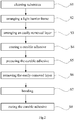
- the process of bonding substrates in one embodiment of present disclosure includes the following steps.
- a surface to be bonded of a first substrate 1 e.g., glass cover plate (CG), touch glass (OGS)
- CG glass cover plate
- OGS touch glass
- a light barrier frame 4 is arranged at a surrounding area of a surface to be bonded of the first substrate 1.
- the light barrier frame 4 may be made of light-absorbing material by means of printing;
- An inside of the light barrier frame 4 is a subsequently-formed light transmitting area of the display device, and the light barrier frame 4 is configured to form a light shielding area of the display device.
- an easily-removed layer 5 is arranged on the light barrier frame 4, i.e., the easily-removed layer 5 is arranged within the light shielding area.
- tensile strength of the easily-removed layer 5 is in a range of 10-30 kgf/mm 2 , thereby guaranteeing that the easily-removed layer may have appropriate strength and the easily-removed layer 5 may be removed completely in a subsequent process of removing.
- the easily-removed layer 5 may be formed by attaching, to the light barrier frame 4, a film formed by polyethylene terephthalate.
- the film configured to form the easily-removed layer 5 may be cut according to a shape of the surface to be bonded of the first substrate 1 to obtain a desired shape, and then is attached to the light barrier frame 4 on the first substrate 1.
- the easily-removed layer 5 may further be formed by printing a peelable adhesive on the light barrier frame 4.
- the peelable adhesive may be printed by means of screen printing.
- the screen printing belongs to the prior art, and the description thereof is omitted herein.
- the peelable adhesive includes light curing or heat curing materials which may be cured after suffering ultraviolet irradiation or heating. In this embodiment, the peelable adhesive is cured after the printing is completed. Curing conditions may be selected based on adopted light curing or heat curing materials.
- the curable adhesive may be an ultraviolet-curing adhesive, e.g., the KAYARAD KSP-501 or Dexerials 12F032-4 ultraviolet-curing adhesive available on market.
- the ultraviolet-curing adhesive is coated on the entire surface to be bonded of the entire first substrate 1 by means of slit coating, to form a curable adhesive layer 2.
- the slit coating belongs to the prior art, and the description thereof is omitted herein.
- the curable adhesive may be a heat curing adhesive.
- the curable adhesive layer 2 formed by the ultraviolet-curing adhesive is precured under ultraviolet-irradiation dose of 100-200mj/cm 2 .
- the curable adhesive is heat curing adhesive
- the substrate on which the heat curing adhesive is coated is heated to perform the procuring.
- Heat curing conditions may be determined based on the adopted heat curing adhesive.
- the easily-removed layer 5 is removed, a part of the curable adhesive layer 2 on the easily-removed layer 5 is also removed, and a remained part of the curable adhesive layer 2 is formed into a desired shape with a uniform thickness, a smooth surface and an edge slope angle approaching to 90°.
- a surface to be bonded of a second substrate 3 (e.g., liquid crystal display panel) is aligned with a surface to be bonded of the first substrate 1, and the two substrates are bonded by the curable adhesive layer 2, to form a touch display panel.
- the first and the second substrates in the embodiment are exemplary rather than restrictive.
- the second substrate 3 may a touch film, a touch glass or a liquid crystal display panel.
- the first substrate is a glass cover plate
- the second substrate may be a touch film or a touch glass; alternatively, when the first substrate is a touch glass, the second substrate may be a liquid crystal display panel; and vice versa.
- the formed curable adhesive layer 2 of the touch display panel is cured by irradiating ultraviolet.
- the ultraviolet-curing adhesive is cured completely by irradiating ultraviolet at a dose of 3500mj/cm 2 , so as to realize a better bonding of the first and the second substrates.
- the curable adhesive layer 2 is formed from heat curing adhesive, the curable adhesive is cured in corresponding heat curing conditions.
- a touch substrate is provided in the embodiment.
- the touch substrate includes a first substrate and a second substrate.
- the first substrate may be a touch substrate
- the second substrate may be a display panel; the touch panel and the display panel are bonded by the above method for bonding substrates.
- the touch substrate provided in the embodiment is manufactured by the above method for bonding substrates, therefore the touch substrate has good optical performance.
- a display device is provided in the embodiment.
- the display device includes a touch substrate.
- the display device provided in the embodiment includes the above touch substrate, therefore the display device has good optical performance.
Abstract
Description
- The present disclosure relates to the field of display technology, in particular to a method for bonding substrates, a touch substrate and a display device.
- At present, electronic products with touch and display functions such as smart phones, computers and televisions have been widely applied. In a process of manufacturing a display screen with touch function of such products, two substrates each provided with functional layers are usually bonded, for example, a touch screen substrate may be bonded to a display panel.
- Generally, a bonding process of bonding the above substrates includes following two types.
- One is a sealant bonding method for bonding substrates by sealant. For example, when a touch screen substrate is bonded to a display panel by such method, the used sealant may be generally provided with a certain thickness, and then a gap may exist between the touch screen and the display panel after the bonding, which may result in that the touch screen and the display panel are not bonded tightly, thereby particulates such as dust are apt to enter into the gap and a touch performance may be influenced, and optical performance of the entire touch module may be worse due to the gap.
- The other method is to bond directly the substrates fully by optical clear adhesive or optical clear resist. For example, when a touch screen substrate is bonded to a display panel by such method, the touch screen and the display panel needs to be cut, and the glass needs to be processed by mean of release filming if the touch screen and the display panel are bonded by the optical clear resist, thereby the cost is high and the operation is complex.
- Comparatively, the cutting operation is not required and a light/heavy release film is used in the bonding by optical clear resist, and a single type of optical clear resist can be applied to various products of different sizes, and a thickness of the resist can be controlled, so the process is relatively simple, therefore such method has been widely applied. The optical clear resist includes a light curing or heat curing materials, which may be cured and cohered after suffering an irradiation or heating accordingly. Up to now, ways of coating optical clear resist for bonding include dispensing coating, screen printing coating and slit coating.
- When the substrates are bonded by means of dispensing coating, the bubbles generated in the process of bonding may be pushed out by making use of flowing of the curable adhesive, and then more adhesive are used, therefore it is difficult to monitor and control phenomenon such as lack of adhesive and adhesive overflow and uniformity of thickness of the curable adhesive; in addition, this method cannot be applied to bonding irregular shapes.
- It is difficult to monitor and control the uniformity of the thickness of the curable adhesive when the substrates are bonded by means of screen printing coating. In addition, a gluing process is complex, and cleaning of jigs is troublesome.
- The thickness of the curable adhesive layer in an intermediate area can be monitored and controlled well in the bonding by means of slit coating, but the curable adhesive layer around the edge is generally thicker than the curable adhesive in the intermediate area, thereby bubbles may be apt to appear around the edge in the process of bonding. In addition, the edge of the curable adhesive may have an obvious slope angle due to gravity of the curable adhesive itself after the process of coating, so phenomenon such as the lack of adhesive/adhesive overflow is difficult to be monitored and controlled in the process of substrates bonding. In addition, the curable adhesive may only be coated into a rectangle rather than irregular shapes.
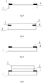
- As shown in
Fig.1 , in the curableadhesive layer 2 configured to bond afirst substrate 1 and asecond substrate 2, bubbles may appear in the curableadhesive layer 2 due to the defects of the above coating. In addition, a curable adhesive slope angle may appear at the edge of the curableadhesive layer 2, and lack of adhesive may appear at an upper part of the slope angle, and adhesive overflow may appear at a lower part thereof. - Therefore, it is desired to improve flatness of the curable
adhesive layer 2, reduce probability of appearance of bubbles, and avoid the lack of adhesive and adhesive overflow appearing at the edge of the curable adhesive layer. - The following issues existing in the related art is to be solved in the present disclosure, including: uniform thicknesses of adhesive layers, bubbles, lack of adhesive and adhesive overflow when bonding different functional substrates in a display device, which may degrade optical performance of the display device. Accordingly, a method for bonding substrate, a touch display panel and a display device are provided.
- The technical scheme to solve the technical issues presented in the present disclosure is a method for bonding substrates, which includes:
- arranging a light barrier frame at a surrounding area of a surface to be bonded of a first substrate;
- arranging an easily-removed layer on the light barrier frame;
- coating curable adhesive on the surface to be bonded of the first substrate;
- precuring the curable adhesive;
- removing the easily-removed layer and simultaneously removing the curable adhesive adhered on the easily-removed layer; and
- bonding a surface to be bonded of a second substrate to the curable adhesive on the first substrate.
- Optionally, the easily-removed layer has a tensile strength in a range of 10-30 kgf/mm2.
- Optionally, the arranging the easily-removed layer on the light barrier frame includes: cutting an easily-removed layer film formed from polyethylene terephthalate into a shape corresponding to the surface to be bonded of the first substrate; and attaching the cut easily-removed layer film to the light barrier frame to form the easily-removed layer.
- Optionally, the arranging the easily-removed layer on the light barrier frame further includes: printing peelable adhesive on the light barrier frame to form the easily-removed layer.
- Optionally, the peelable adhesive includes light curing or heat curing material.
- Optionally, after printing the peelable adhesive to form the easily-removed layer, the method further includes: precuring the easily-removed layer.
- Optionally, the curable adhesive is an ultraviolet-curing adhesive; the precuring includes irradiating the curable adhesive with ultraviolet at a dose of 100-200mj/cm2.
- Optionally, after bonding the second substrate, the method further includes: curing the curable adhesive.
- Optionally, the first substrate is a glass cover plate, and the second substrate is a touch film or a touch glass; or the first substrate is a touch glass, and the second substrate is a liquid crystal display panel.
- A touch substrate is further provided by the present disclosure, including a first substrate and a second substrate. The first and the second substrates are bonded by the above method for bonding substrates.
- A display device is further provided by the present disclosure, including the above touch substrate.
- In the process of manufacturing a touch display panel and a display device by the method for bonding substrates provided in the present disclosure, by steps such as arranging an easily-removed layer at a surrounding of a first substrate, coating and precuring a light curing adhesive, removing the easily-removed layer, the light curing adhesive may be formed into a desired shape (including irregular shapes). In addition, an adhesive layer of the light curing adhesive has a uniform thickness, smooth surface and an edge slope angle approaching to 90°. Furthermore, bonding bubbles may be reduced, and phenomenon such as lack of adhesive and adhesive overflow may be suppressed in the bonding process, thereby guaranteeing optical performance of the display device.
-
-
Fig. 1 is a schematic view showing a bonding state of substrates in the related art; -
Fig. 2 is a flow chart of a method for bonding substrates according to the present disclosure; -
Fig.3 is a schematic view showing a structure of a first substrate provided with an easily-removed layer according to one embodiment of the present disclosure; -
Fig.4 is a schematic view showing a structure of the first substrate coated with curable adhesive according to one embodiment of the present disclosure; -
Fig.5 is a schematic view showing a structure of the first substrate from which the easily-removed layer is removed according to one embodiment of the present disclosure; and -
Fig.6 is a schematic view showing a structure of the first substrate and a second substrate which are bonded together according to one embodiment of the present disclosure. - 1. first substrate; 2. curable adhesive layer; 3. second substrate; 4. light barrier frame; 5. easily-removed layer
- To make the technical schemes better understood by those skilled in the art, the present disclosure may be described in details in conjunction with drawings and embodiments.
- A method for bonding substrates is provided in the embodiment and includes:
- arranging a light barrier frame at a surrounding area of a surface to be bonded of a first substrate;
- arranging an easily-removed layer on the light barrier frame;
- coating curable adhesive on the surface to be bonded of the first substrate;
- precuring the curable adhesive;
- removing the easily-removed layer and simultaneously removing the curable adhesive adhered on the easily-removed layer; and
- bonding a surface to be bonded of a second substrate and the curable adhesive on the first substrate.
- When manufacturing a touch display panel and a display device by the method of bonding substrates provided in the present disclosure, by the steps such as arranging the easily-removed layer at the surrounding of the first substrate, coating and precuring a light-curing adhesive and removing the easily-removed layer, the light-curing adhesive may be formed into a required shape (including irregular shapes). Further, an adhesive layer of the light-curing adhesive has a uniform thickness, a smooth surface and an edge slope angle approaching to 90°. Furthermore, bonding bubbles may be effectively reduced, and phenomenon such as lack of adhesive and adhesive overflow may be suppressed in the bonding process, thereby guaranteeing optical performance of the display device.
- To be specific, as shown in
Fig.2 , the process of bonding substrates in one embodiment of present disclosure includes the following steps. - To be specific, a surface to be bonded of a first substrate 1 (e.g., glass cover plate (CG), touch glass (OGS)) is cleaned by means of plasma cleaning. The method of plasma cleaning belongs to the prior art, and the description thereof is omitted herein.
- To be specific, as shown in
Fig.3 , alight barrier frame 4 is arranged at a surrounding area of a surface to be bonded of thefirst substrate 1. Thelight barrier frame 4 may be made of light-absorbing material by means of printing; - An inside of the
light barrier frame 4 is a subsequently-formed light transmitting area of the display device, and thelight barrier frame 4 is configured to form a light shielding area of the display device. - To be specific, as shown in
Fig.3 , an easily-removedlayer 5 is arranged on thelight barrier frame 4, i.e., the easily-removedlayer 5 is arranged within the light shielding area. - Alternatively, tensile strength of the easily-removed
layer 5 is in a range of 10-30 kgf/mm2, thereby guaranteeing that the easily-removed layer may have appropriate strength and the easily-removedlayer 5 may be removed completely in a subsequent process of removing. - Alternatively, the easily-removed
layer 5 may be formed by attaching, to thelight barrier frame 4, a film formed by polyethylene terephthalate. - In the process of attaching the easily-removed
layer 5, the film configured to form the easily-removedlayer 5 may be cut according to a shape of the surface to be bonded of thefirst substrate 1 to obtain a desired shape, and then is attached to thelight barrier frame 4 on thefirst substrate 1. - It should be understood that the easily-removed
layer 5 may further be formed by printing a peelable adhesive on thelight barrier frame 4. For example, the peelable adhesive may be printed by means of screen printing. The screen printing belongs to the prior art, and the description thereof is omitted herein. The peelable adhesive includes light curing or heat curing materials which may be cured after suffering ultraviolet irradiation or heating. In this embodiment, the peelable adhesive is cured after the printing is completed. Curing conditions may be selected based on adopted light curing or heat curing materials. - To be specific, as shown in
Fig.4 , the curable adhesive may be an ultraviolet-curing adhesive, e.g., the KAYARAD KSP-501 or Dexerials 12F032-4 ultraviolet-curing adhesive available on market. The ultraviolet-curing adhesive is coated on the entire surface to be bonded of the entirefirst substrate 1 by means of slit coating, to form a curableadhesive layer 2. The slit coating belongs to the prior art, and the description thereof is omitted herein. - It should be understood that the curable adhesive may be a heat curing adhesive.
- To be specific, the curable
adhesive layer 2 formed by the ultraviolet-curing adhesive is precured under ultraviolet-irradiation dose of 100-200mj/cm2. - It should be understood that, when the curable adhesive is heat curing adhesive, the substrate on which the heat curing adhesive is coated is heated to perform the procuring. Heat curing conditions may be determined based on the adopted heat curing adhesive.
- To be specific, as shown in
Fig.5 , the easily-removedlayer 5 is removed, a part of the curableadhesive layer 2 on the easily-removedlayer 5 is also removed, and a remained part of the curableadhesive layer 2 is formed into a desired shape with a uniform thickness, a smooth surface and an edge slope angle approaching to 90°. - To be specific, as shown in
Fig.6 , a surface to be bonded of a second substrate 3 (e.g., liquid crystal display panel) is aligned with a surface to be bonded of thefirst substrate 1, and the two substrates are bonded by the curableadhesive layer 2, to form a touch display panel. It should be noted that, the first and the second substrates in the embodiment are exemplary rather than restrictive. For example, thesecond substrate 3 may a touch film, a touch glass or a liquid crystal display panel. When the first substrate is a glass cover plate, the second substrate may be a touch film or a touch glass; alternatively, when the first substrate is a touch glass, the second substrate may be a liquid crystal display panel; and vice versa. - To be specific, the formed curable
adhesive layer 2 of the touch display panel is cured by irradiating ultraviolet. For example, the ultraviolet-curing adhesive is cured completely by irradiating ultraviolet at a dose of 3500mj/cm2, so as to realize a better bonding of the first and the second substrates. - It should be noted that, when the curable
adhesive layer 2 is formed from heat curing adhesive, the curable adhesive is cured in corresponding heat curing conditions. - Alternatively, other functional layers are further formed on the above display panel formed by means of bonding, so as to complete the manufacturing of the display device.
- A touch substrate is provided in the embodiment. The touch substrate includes a first substrate and a second substrate. The first substrate may be a touch substrate, and the second substrate may be a display panel; the touch panel and the display panel are bonded by the above method for bonding substrates.
- The touch substrate provided in the embodiment is manufactured by the above method for bonding substrates, therefore the touch substrate has good optical performance.
- A display device is provided in the embodiment. The display device includes a touch substrate.
- The display device provided in the embodiment includes the above touch substrate, therefore the display device has good optical performance.
- It may be understood that, the above embodiments are merely the examplary embodiments for illustrating principles of the present disclosure, but the present disclosure is not limited thereto. Those skilled in the art may make various modifications and improvements without departing from the spirit and essence of the present disclosure, and these modifications and improvements may also fall into the scope of the present disclosure.
Claims (11)
- A method for bonding substrates, comprising:arranging a light barrier frame at a surrounding area of a surface to be bonded of a first substrate;arranging an easily-removed layer on the light barrier frame;coating curable adhesive on the surface to be bonded of the first substrate;precuring the curable adhesive;removing the easily-removed layer and simultaneously removing the curable adhesive adhered on the easily-removed layer; andbonding a surface to be bonded of a second substrate to the curable adhesive on the first substrate.
- The method according to claim 1, wherein the easily-removed layer has a tensile strength in a range of 10-30 kgf/mm2.
- The method according to claim 1, wherein the arranging the easily-removed layer on the light barrier frame comprises:cutting an easily-removed layer film formed from polyethylene terephthalate into a shape corresponding to the surface to be bonded of the first substrate; andattaching the cut easily-removed layer film to the light barrier frame to form the easily-removed layer.
- The method according to claim 1, wherein the arranging the easily-removed layer on the light barrier frame comprises:printing peelable adhesive on the light barrier frame to form the easily-removed layer.
- The method according to claim 4, wherein the peelable adhesive comprises light curing or heat curing material.
- The method according to claim 5, wherein after printing the peelable adhesive to form the easily-removed layer, the method further comprises:curing the easily-removed layer.
- The method according to claim 1, wherein the curable adhesive is ultraviolet-curing adhesive; the procuring comprises irradiating the curable adhesive with ultraviolet at a dose of 100-200mj/cm2.
- The method according to claim 1, wherein after bonding the second substrate, the method further comprises:curing the curable adhesive.
- The method according to claim 1, wherein the first substrate is a glass cover plate, and the second substrate is a touch film or a touch glass; or
the first substrate is a touch glass, and the second substrate is a liquid crystal display panel. - A touch substrate, comprising a first substrate and a second substrate; wherein the first and the second substrates are bonded by the method for bonding substrates according to any one of claims 1-9.
- A display device comprising the touch substrate according to claim 10.
Applications Claiming Priority (2)
| Application Number | Priority Date | Filing Date | Title |
|---|---|---|---|
| CN201410476433.4A CN104309267B (en) | 2014-09-17 | 2014-09-17 | A kind of method for bonding substrate, touch display substrate, display device |
| PCT/CN2015/070614 WO2016041307A1 (en) | 2014-09-17 | 2015-01-13 | Substrate bonding method, touch control substrate and display device |
Publications (3)
| Publication Number | Publication Date |
|---|---|
| EP3196018A1 true EP3196018A1 (en) | 2017-07-26 |
| EP3196018A4 EP3196018A4 (en) | 2018-05-09 |
| EP3196018B1 EP3196018B1 (en) | 2019-07-17 |
Family
ID=52364642
Family Applications (1)
| Application Number | Title | Priority Date | Filing Date |
|---|---|---|---|
| EP15753302.7A Active EP3196018B1 (en) | 2014-09-17 | 2015-01-13 | Substrate bonding method |
Country Status (4)
| Country | Link |
|---|---|
| US (1) | US20160361907A1 (en) |
| EP (1) | EP3196018B1 (en) |
| CN (1) | CN104309267B (en) |
| WO (1) | WO2016041307A1 (en) |
Families Citing this family (14)
| Publication number | Priority date | Publication date | Assignee | Title |
|---|---|---|---|---|
| JP6216727B2 (en) * | 2014-05-08 | 2017-10-18 | 東京応化工業株式会社 | Support separation method |
| CN105094415B (en) * | 2015-04-29 | 2018-02-23 | 业成光电(深圳)有限公司 | Touch control display apparatus |
| CN105068697A (en) * | 2015-09-23 | 2015-11-18 | 京东方科技集团股份有限公司 | Single-chip touch panel and manufacturing method thereof, as well as touch screen and touch display device |
| CN105629536B (en) * | 2016-03-31 | 2018-12-18 | 中航华东光电有限公司 | Firmly to hard liquid crystal display binding method |
| ES2931049T3 (en) * | 2017-11-03 | 2022-12-23 | E Ink Corp | Production processes of electro-optical display devices |
| CN108909223A (en) * | 2018-06-29 | 2018-11-30 | 东莞市晶博光电有限公司 | A kind of preparation process of glass cover-plate |
| CN109094227A (en) * | 2018-06-29 | 2018-12-28 | 东莞市晶博光电有限公司 | A kind of technique of the silk-screen IR on glass cover-plate |
| CN110760896A (en) * | 2018-07-26 | 2020-02-07 | 苏州苏大维格科技集团股份有限公司 | Crease-resistant electroforming process for working plate |
| CN109823005B (en) * | 2019-01-29 | 2021-09-17 | 信利光电股份有限公司 | Solid optical adhesive full-lamination method |
| CN110901044B (en) * | 2019-11-29 | 2022-07-19 | 京东方科技集团股份有限公司 | A laminating frock for curved surface screen |
| CN111258094A (en) * | 2020-02-12 | 2020-06-09 | 京东方科技集团股份有限公司 | Display module gluing assembly method and device |
| JP2022047865A (en) * | 2020-09-14 | 2022-03-25 | 株式会社飯沼ゲージ製作所 | Device and method for workpiece bonding |
| CN113820875A (en) * | 2021-09-01 | 2021-12-21 | 滁州桐友显示科技有限公司 | Bonding method and display module |
| CN116431023A (en) | 2023-04-13 | 2023-07-14 | 达擎股份有限公司 | Display device |
Family Cites Families (12)
| Publication number | Priority date | Publication date | Assignee | Title |
|---|---|---|---|---|
| US4826705A (en) * | 1986-07-02 | 1989-05-02 | Loctite Corporation | Radiation curable temporary solder mask |
| JP2002121502A (en) * | 2000-10-16 | 2002-04-26 | Panac Co Ltd | Sheet type adhesive laminate for liquid crystal element manufacturing process |
| GB2425401A (en) * | 2005-04-21 | 2006-10-25 | Stuart Philip Speakman | Manufacture of microstructures using peelable mask |
| JP5188833B2 (en) * | 2008-02-21 | 2013-04-24 | 株式会社ジャパンディスプレイイースト | Manufacturing method of display device |
| TWI615743B (en) * | 2010-03-25 | 2018-02-21 | Winsky Tech Limited | Touch panel and method of manufacturing same |
| KR101094151B1 (en) * | 2011-03-03 | 2011-12-14 | 에쓰이에이치에프코리아 (주) | Method for fabricating transparent circuit substrate for touchscreen |
| JP5368516B2 (en) * | 2011-07-13 | 2013-12-18 | 岐阜車体工業株式会社 | Seat slide device |
| KR20140103184A (en) * | 2011-10-21 | 2014-08-25 | 니폰 가야꾸 가부시끼가이샤 | Method for producing optical member and use of uv-curable resin composition therefor |
| US9266310B2 (en) * | 2011-12-16 | 2016-02-23 | Apple Inc. | Methods of joining device structures with adhesive |
| CN105807468B (en) * | 2012-01-25 | 2020-09-11 | 迪睿合电子材料有限公司 | Method for manufacturing image display device |
| CN103294241B (en) * | 2012-03-05 | 2016-04-06 | 冠伟科技股份有限公司 | The method of baseplate-laminating |
| CN103970349A (en) * | 2014-03-10 | 2014-08-06 | 业成光电(深圳)有限公司 | Touch control device and attaching type manufacturing process thereof |
-
2014
- 2014-09-17 CN CN201410476433.4A patent/CN104309267B/en not_active Expired - Fee Related
-
2015
- 2015-01-13 WO PCT/CN2015/070614 patent/WO2016041307A1/en active Application Filing
- 2015-01-13 US US14/771,429 patent/US20160361907A1/en not_active Abandoned
- 2015-01-13 EP EP15753302.7A patent/EP3196018B1/en active Active
Also Published As
| Publication number | Publication date |
|---|---|
| US20160361907A1 (en) | 2016-12-15 |
| CN104309267A (en) | 2015-01-28 |
| EP3196018A4 (en) | 2018-05-09 |
| WO2016041307A1 (en) | 2016-03-24 |
| EP3196018B1 (en) | 2019-07-17 |
| CN104309267B (en) | 2016-08-17 |
Similar Documents
| Publication | Publication Date | Title |
|---|---|---|
| EP3196018B1 (en) | Substrate bonding method | |
| KR101827808B1 (en) | Integrated fully-sealed liquid crystal screen and manufacturing process for same | |
| US10429971B2 (en) | Display panel, manufacturing method thereof and display device | |
| CN103160214A (en) | Manufacturing method of bonding device | |
| KR20160008307A (en) | Method for manufacturing display module using optically clear resin | |
| JP2015232656A (en) | Apparatus and manufacturing method therefor | |
| CN102636915A (en) | Liquid crystal display panel and manufacturing method thereof | |
| WO2016065802A1 (en) | Method for attaching first panel and second panel and display device | |
| JP2011053308A (en) | Display device and method of manufacturing the same | |
| US9256130B2 (en) | Method for manufacturing light-shielding mask for curing cell sealant | |
| US10150279B2 (en) | Panel laminating method, panel assembly and electronic device | |
| CN102736324B (en) | Photomask solidified by frame glue and manufacturing method of liquid crystal display panel | |
| EP3605216B1 (en) | Glue sealing method for display screen frame | |
| CN101702402B (en) | Glue overflow-preventing device and baseplate-laminating method using same | |
| WO2016026208A1 (en) | Manufacturing method of flexible display and flexible display | |
| JP2016038559A (en) | Apparatus and manufacturing method of apparatus | |
| WO2015024333A1 (en) | Sealant coating device and method, and method for achieving alignment | |
| TWI530396B (en) | Panel laminating method, panel assembly and electronic device | |
| CN104298013A (en) | Combination method of array substrate and color film substrate | |
| KR20130032626A (en) | Uv lamination jig and uv lamination method using the jig | |
| US20120276801A1 (en) | Transporting device and display panel assembly apparatus and method using the same | |
| CN102148170B (en) | Substrate adhesion method | |
| WO2017185825A1 (en) | Panel and processing method thereof | |
| KR101274096B1 (en) | Method for evacuating bubble | |
| CN107450217B (en) | Substrate, method for manufacturing substrate, and method for dividing display panel |
Legal Events
| Date | Code | Title | Description |
|---|---|---|---|
| PUAI | Public reference made under article 153(3) epc to a published international application that has entered the european phase |
Free format text: ORIGINAL CODE: 0009012 |
|
| STAA | Information on the status of an ep patent application or granted ep patent |
Free format text: STATUS: REQUEST FOR EXAMINATION WAS MADE |
|
| 17P | Request for examination filed |
Effective date: 20150831 |
|
| AK | Designated contracting states |
Kind code of ref document: A1 Designated state(s): AL AT BE BG CH CY CZ DE DK EE ES FI FR GB GR HR HU IE IS IT LI LT LU LV MC MK MT NL NO PL PT RO RS SE SI SK SM TR |
|
| AX | Request for extension of the european patent |
Extension state: BA ME |
|
| DAX | Request for extension of the european patent (deleted) | ||
| A4 | Supplementary search report drawn up and despatched |
Effective date: 20180410 |
|
| RIC1 | Information provided on ipc code assigned before grant |
Ipc: B32B 37/12 20060101AFI20180404BHEP Ipc: B32B 37/00 20060101ALI20180404BHEP Ipc: G02F 1/1333 20060101ALI20180404BHEP |
|
| GRAP | Despatch of communication of intention to grant a patent |
Free format text: ORIGINAL CODE: EPIDOSNIGR1 |
|
| STAA | Information on the status of an ep patent application or granted ep patent |
Free format text: STATUS: GRANT OF PATENT IS INTENDED |
|
| INTG | Intention to grant announced |
Effective date: 20190222 |
|
| GRAS | Grant fee paid |
Free format text: ORIGINAL CODE: EPIDOSNIGR3 |
|
| GRAA | (expected) grant |
Free format text: ORIGINAL CODE: 0009210 |
|
| STAA | Information on the status of an ep patent application or granted ep patent |
Free format text: STATUS: THE PATENT HAS BEEN GRANTED |
|
| AK | Designated contracting states |
Kind code of ref document: B1 Designated state(s): AL AT BE BG CH CY CZ DE DK EE ES FI FR GB GR HR HU IE IS IT LI LT LU LV MC MK MT NL NO PL PT RO RS SE SI SK SM TR |
|
| REG | Reference to a national code |
Ref country code: GB Ref legal event code: FG4D |
|
| REG | Reference to a national code |
Ref country code: CH Ref legal event code: EP |
|
| REG | Reference to a national code |
Ref country code: IE Ref legal event code: FG4D |
|
| REG | Reference to a national code |
Ref country code: DE Ref legal event code: R096 Ref document number: 602015033933 Country of ref document: DE |
|
| REG | Reference to a national code |
Ref country code: AT Ref legal event code: REF Ref document number: 1155463 Country of ref document: AT Kind code of ref document: T Effective date: 20190815 |
|
| REG | Reference to a national code |
Ref country code: NL Ref legal event code: FP |
|
| REG | Reference to a national code |
Ref country code: LT Ref legal event code: MG4D |
|
| REG | Reference to a national code |
Ref country code: AT Ref legal event code: MK05 Ref document number: 1155463 Country of ref document: AT Kind code of ref document: T Effective date: 20190717 |
|
| PG25 | Lapsed in a contracting state [announced via postgrant information from national office to epo] |
Ref country code: AT Free format text: LAPSE BECAUSE OF FAILURE TO SUBMIT A TRANSLATION OF THE DESCRIPTION OR TO PAY THE FEE WITHIN THE PRESCRIBED TIME-LIMIT Effective date: 20190717 Ref country code: NO Free format text: LAPSE BECAUSE OF FAILURE TO SUBMIT A TRANSLATION OF THE DESCRIPTION OR TO PAY THE FEE WITHIN THE PRESCRIBED TIME-LIMIT Effective date: 20191017 Ref country code: HR Free format text: LAPSE BECAUSE OF FAILURE TO SUBMIT A TRANSLATION OF THE DESCRIPTION OR TO PAY THE FEE WITHIN THE PRESCRIBED TIME-LIMIT Effective date: 20190717 Ref country code: FI Free format text: LAPSE BECAUSE OF FAILURE TO SUBMIT A TRANSLATION OF THE DESCRIPTION OR TO PAY THE FEE WITHIN THE PRESCRIBED TIME-LIMIT Effective date: 20190717 Ref country code: SE Free format text: LAPSE BECAUSE OF FAILURE TO SUBMIT A TRANSLATION OF THE DESCRIPTION OR TO PAY THE FEE WITHIN THE PRESCRIBED TIME-LIMIT Effective date: 20190717 Ref country code: LT Free format text: LAPSE BECAUSE OF FAILURE TO SUBMIT A TRANSLATION OF THE DESCRIPTION OR TO PAY THE FEE WITHIN THE PRESCRIBED TIME-LIMIT Effective date: 20190717 Ref country code: PT Free format text: LAPSE BECAUSE OF FAILURE TO SUBMIT A TRANSLATION OF THE DESCRIPTION OR TO PAY THE FEE WITHIN THE PRESCRIBED TIME-LIMIT Effective date: 20191118 Ref country code: BG Free format text: LAPSE BECAUSE OF FAILURE TO SUBMIT A TRANSLATION OF THE DESCRIPTION OR TO PAY THE FEE WITHIN THE PRESCRIBED TIME-LIMIT Effective date: 20191017 |
|
| PG25 | Lapsed in a contracting state [announced via postgrant information from national office to epo] |
Ref country code: LV Free format text: LAPSE BECAUSE OF FAILURE TO SUBMIT A TRANSLATION OF THE DESCRIPTION OR TO PAY THE FEE WITHIN THE PRESCRIBED TIME-LIMIT Effective date: 20190717 Ref country code: GR Free format text: LAPSE BECAUSE OF FAILURE TO SUBMIT A TRANSLATION OF THE DESCRIPTION OR TO PAY THE FEE WITHIN THE PRESCRIBED TIME-LIMIT Effective date: 20191018 Ref country code: RS Free format text: LAPSE BECAUSE OF FAILURE TO SUBMIT A TRANSLATION OF THE DESCRIPTION OR TO PAY THE FEE WITHIN THE PRESCRIBED TIME-LIMIT Effective date: 20190717 Ref country code: ES Free format text: LAPSE BECAUSE OF FAILURE TO SUBMIT A TRANSLATION OF THE DESCRIPTION OR TO PAY THE FEE WITHIN THE PRESCRIBED TIME-LIMIT Effective date: 20190717 Ref country code: AL Free format text: LAPSE BECAUSE OF FAILURE TO SUBMIT A TRANSLATION OF THE DESCRIPTION OR TO PAY THE FEE WITHIN THE PRESCRIBED TIME-LIMIT Effective date: 20190717 Ref country code: IS Free format text: LAPSE BECAUSE OF FAILURE TO SUBMIT A TRANSLATION OF THE DESCRIPTION OR TO PAY THE FEE WITHIN THE PRESCRIBED TIME-LIMIT Effective date: 20191117 |
|
| PG25 | Lapsed in a contracting state [announced via postgrant information from national office to epo] |
Ref country code: TR Free format text: LAPSE BECAUSE OF FAILURE TO SUBMIT A TRANSLATION OF THE DESCRIPTION OR TO PAY THE FEE WITHIN THE PRESCRIBED TIME-LIMIT Effective date: 20190717 |
|
| PG25 | Lapsed in a contracting state [announced via postgrant information from national office to epo] |
Ref country code: PL Free format text: LAPSE BECAUSE OF FAILURE TO SUBMIT A TRANSLATION OF THE DESCRIPTION OR TO PAY THE FEE WITHIN THE PRESCRIBED TIME-LIMIT Effective date: 20190717 Ref country code: RO Free format text: LAPSE BECAUSE OF FAILURE TO SUBMIT A TRANSLATION OF THE DESCRIPTION OR TO PAY THE FEE WITHIN THE PRESCRIBED TIME-LIMIT Effective date: 20190717 Ref country code: EE Free format text: LAPSE BECAUSE OF FAILURE TO SUBMIT A TRANSLATION OF THE DESCRIPTION OR TO PAY THE FEE WITHIN THE PRESCRIBED TIME-LIMIT Effective date: 20190717 Ref country code: IT Free format text: LAPSE BECAUSE OF FAILURE TO SUBMIT A TRANSLATION OF THE DESCRIPTION OR TO PAY THE FEE WITHIN THE PRESCRIBED TIME-LIMIT Effective date: 20190717 Ref country code: DK Free format text: LAPSE BECAUSE OF FAILURE TO SUBMIT A TRANSLATION OF THE DESCRIPTION OR TO PAY THE FEE WITHIN THE PRESCRIBED TIME-LIMIT Effective date: 20190717 |
|
| PG25 | Lapsed in a contracting state [announced via postgrant information from national office to epo] |
Ref country code: SM Free format text: LAPSE BECAUSE OF FAILURE TO SUBMIT A TRANSLATION OF THE DESCRIPTION OR TO PAY THE FEE WITHIN THE PRESCRIBED TIME-LIMIT Effective date: 20190717 Ref country code: IS Free format text: LAPSE BECAUSE OF FAILURE TO SUBMIT A TRANSLATION OF THE DESCRIPTION OR TO PAY THE FEE WITHIN THE PRESCRIBED TIME-LIMIT Effective date: 20200224 Ref country code: CZ Free format text: LAPSE BECAUSE OF FAILURE TO SUBMIT A TRANSLATION OF THE DESCRIPTION OR TO PAY THE FEE WITHIN THE PRESCRIBED TIME-LIMIT Effective date: 20190717 Ref country code: SK Free format text: LAPSE BECAUSE OF FAILURE TO SUBMIT A TRANSLATION OF THE DESCRIPTION OR TO PAY THE FEE WITHIN THE PRESCRIBED TIME-LIMIT Effective date: 20190717 |
|
| REG | Reference to a national code |
Ref country code: DE Ref legal event code: R097 Ref document number: 602015033933 Country of ref document: DE |
|
| PLBE | No opposition filed within time limit |
Free format text: ORIGINAL CODE: 0009261 |
|
| STAA | Information on the status of an ep patent application or granted ep patent |
Free format text: STATUS: NO OPPOSITION FILED WITHIN TIME LIMIT |
|
| PG2D | Information on lapse in contracting state deleted |
Ref country code: IS |
|
| 26N | No opposition filed |
Effective date: 20200603 |
|
| PG25 | Lapsed in a contracting state [announced via postgrant information from national office to epo] |
Ref country code: MC Free format text: LAPSE BECAUSE OF FAILURE TO SUBMIT A TRANSLATION OF THE DESCRIPTION OR TO PAY THE FEE WITHIN THE PRESCRIBED TIME-LIMIT Effective date: 20190717 Ref country code: SI Free format text: LAPSE BECAUSE OF FAILURE TO SUBMIT A TRANSLATION OF THE DESCRIPTION OR TO PAY THE FEE WITHIN THE PRESCRIBED TIME-LIMIT Effective date: 20190717 |
|
| REG | Reference to a national code |
Ref country code: CH Ref legal event code: PL |
|
| REG | Reference to a national code |
Ref country code: BE Ref legal event code: MM Effective date: 20200131 |
|
| PG25 | Lapsed in a contracting state [announced via postgrant information from national office to epo] |
Ref country code: LU Free format text: LAPSE BECAUSE OF NON-PAYMENT OF DUE FEES Effective date: 20200113 |
|
| PG25 | Lapsed in a contracting state [announced via postgrant information from national office to epo] |
Ref country code: BE Free format text: LAPSE BECAUSE OF NON-PAYMENT OF DUE FEES Effective date: 20200131 Ref country code: LI Free format text: LAPSE BECAUSE OF NON-PAYMENT OF DUE FEES Effective date: 20200131 Ref country code: CH Free format text: LAPSE BECAUSE OF NON-PAYMENT OF DUE FEES Effective date: 20200131 |
|
| PG25 | Lapsed in a contracting state [announced via postgrant information from national office to epo] |
Ref country code: IE Free format text: LAPSE BECAUSE OF NON-PAYMENT OF DUE FEES Effective date: 20200113 |
|
| PGFP | Annual fee paid to national office [announced via postgrant information from national office to epo] |
Ref country code: FR Payment date: 20210122 Year of fee payment: 7 Ref country code: NL Payment date: 20210120 Year of fee payment: 7 |
|
| PGFP | Annual fee paid to national office [announced via postgrant information from national office to epo] |
Ref country code: DE Payment date: 20210120 Year of fee payment: 7 Ref country code: GB Payment date: 20210121 Year of fee payment: 7 |
|
| PG25 | Lapsed in a contracting state [announced via postgrant information from national office to epo] |
Ref country code: MT Free format text: LAPSE BECAUSE OF FAILURE TO SUBMIT A TRANSLATION OF THE DESCRIPTION OR TO PAY THE FEE WITHIN THE PRESCRIBED TIME-LIMIT Effective date: 20190717 Ref country code: CY Free format text: LAPSE BECAUSE OF FAILURE TO SUBMIT A TRANSLATION OF THE DESCRIPTION OR TO PAY THE FEE WITHIN THE PRESCRIBED TIME-LIMIT Effective date: 20190717 |
|
| PG25 | Lapsed in a contracting state [announced via postgrant information from national office to epo] |
Ref country code: MK Free format text: LAPSE BECAUSE OF FAILURE TO SUBMIT A TRANSLATION OF THE DESCRIPTION OR TO PAY THE FEE WITHIN THE PRESCRIBED TIME-LIMIT Effective date: 20190717 |
|
| REG | Reference to a national code |
Ref country code: DE Ref legal event code: R119 Ref document number: 602015033933 Country of ref document: DE |
|
| REG | Reference to a national code |
Ref country code: NL Ref legal event code: MM Effective date: 20220201 |
|
| GBPC | Gb: european patent ceased through non-payment of renewal fee |
Effective date: 20220113 |
|
| PG25 | Lapsed in a contracting state [announced via postgrant information from national office to epo] |
Ref country code: NL Free format text: LAPSE BECAUSE OF NON-PAYMENT OF DUE FEES Effective date: 20220201 Ref country code: GB Free format text: LAPSE BECAUSE OF NON-PAYMENT OF DUE FEES Effective date: 20220113 Ref country code: DE Free format text: LAPSE BECAUSE OF NON-PAYMENT OF DUE FEES Effective date: 20220802 |
|
| PG25 | Lapsed in a contracting state [announced via postgrant information from national office to epo] |
Ref country code: FR Free format text: LAPSE BECAUSE OF NON-PAYMENT OF DUE FEES Effective date: 20220131 |