EP3195506B1 - Optical transmitters and receivers using polarization multiplexing - Google Patents
Optical transmitters and receivers using polarization multiplexing Download PDFInfo
- Publication number
- EP3195506B1 EP3195506B1 EP15784769.0A EP15784769A EP3195506B1 EP 3195506 B1 EP3195506 B1 EP 3195506B1 EP 15784769 A EP15784769 A EP 15784769A EP 3195506 B1 EP3195506 B1 EP 3195506B1
- Authority
- EP
- European Patent Office
- Prior art keywords
- optical
- polarization
- signal
- intensity
- modulated
- Prior art date
- Legal status (The legal status is an assumption and is not a legal conclusion. Google has not performed a legal analysis and makes no representation as to the accuracy of the status listed.)
- Active
Links
Images




Classifications
-
- H—ELECTRICITY
- H04—ELECTRIC COMMUNICATION TECHNIQUE
- H04J—MULTIPLEX COMMUNICATION
- H04J14/00—Optical multiplex systems
- H04J14/06—Polarisation multiplex systems
-
- H—ELECTRICITY
- H04—ELECTRIC COMMUNICATION TECHNIQUE
- H04B—TRANSMISSION
- H04B10/00—Transmission systems employing electromagnetic waves other than radio-waves, e.g. infrared, visible or ultraviolet light, or employing corpuscular radiation, e.g. quantum communication
- H04B10/50—Transmitters
- H04B10/516—Details of coding or modulation
- H04B10/532—Polarisation modulation
-
- H—ELECTRICITY
- H04—ELECTRIC COMMUNICATION TECHNIQUE
- H04B—TRANSMISSION
- H04B10/00—Transmission systems employing electromagnetic waves other than radio-waves, e.g. infrared, visible or ultraviolet light, or employing corpuscular radiation, e.g. quantum communication
- H04B10/50—Transmitters
- H04B10/516—Details of coding or modulation
- H04B10/54—Intensity modulation
- H04B10/541—Digital intensity or amplitude modulation
-
- H—ELECTRICITY
- H04—ELECTRIC COMMUNICATION TECHNIQUE
- H04B—TRANSMISSION
- H04B10/00—Transmission systems employing electromagnetic waves other than radio-waves, e.g. infrared, visible or ultraviolet light, or employing corpuscular radiation, e.g. quantum communication
- H04B10/50—Transmitters
- H04B10/516—Details of coding or modulation
- H04B10/548—Phase or frequency modulation
- H04B10/556—Digital modulation, e.g. differential phase shift keying [DPSK] or frequency shift keying [FSK]
- H04B10/5561—Digital phase modulation
-
- H—ELECTRICITY
- H04—ELECTRIC COMMUNICATION TECHNIQUE
- H04B—TRANSMISSION
- H04B10/00—Transmission systems employing electromagnetic waves other than radio-waves, e.g. infrared, visible or ultraviolet light, or employing corpuscular radiation, e.g. quantum communication
- H04B10/60—Receivers
-
- H—ELECTRICITY
- H04—ELECTRIC COMMUNICATION TECHNIQUE
- H04B—TRANSMISSION
- H04B10/00—Transmission systems employing electromagnetic waves other than radio-waves, e.g. infrared, visible or ultraviolet light, or employing corpuscular radiation, e.g. quantum communication
- H04B10/60—Receivers
- H04B10/61—Coherent receivers
- H04B10/614—Coherent receivers comprising one or more polarization beam splitters, e.g. polarization multiplexed [PolMux] X-PSK coherent receivers, polarization diversity heterodyne coherent receivers
-
- H—ELECTRICITY
- H04—ELECTRIC COMMUNICATION TECHNIQUE
- H04B—TRANSMISSION
- H04B10/00—Transmission systems employing electromagnetic waves other than radio-waves, e.g. infrared, visible or ultraviolet light, or employing corpuscular radiation, e.g. quantum communication
- H04B10/60—Receivers
- H04B10/61—Coherent receivers
- H04B10/616—Details of the electronic signal processing in coherent optical receivers
-
- H—ELECTRICITY
- H04—ELECTRIC COMMUNICATION TECHNIQUE
- H04B—TRANSMISSION
- H04B10/00—Transmission systems employing electromagnetic waves other than radio-waves, e.g. infrared, visible or ultraviolet light, or employing corpuscular radiation, e.g. quantum communication
- H04B10/40—Transceivers
-
- H—ELECTRICITY
- H04—ELECTRIC COMMUNICATION TECHNIQUE
- H04B—TRANSMISSION
- H04B10/00—Transmission systems employing electromagnetic waves other than radio-waves, e.g. infrared, visible or ultraviolet light, or employing corpuscular radiation, e.g. quantum communication
- H04B10/50—Transmitters
Definitions
- the present application relates generally to optical transmitters and receivers, and more particularly relates to optical transmitter and receiver devices using polarization multiplexing.
- Optical interconnects for short reach applications such as intra-data center information transport need to support more data throughput.
- Approaches should be cost effective, energy efficient, and require a small footprint.
- the use of a single-laser transmitter and a receiver having a passive optical receiver front-end and using direct detection should be employed.
- Demonstrations of 100 Gbps per wavelength have been reported for short-range transmissions, using various modulation formats.
- Some experiments employed polarization-division multiplexing (PDM) to halve the desired baud rate, i.e., the number of symbols per second, to reach 100 Gbps, with the polarization demultiplexing done optically, with a polarization controller/stabilizer.
- PDM polarization-division multiplexing
- Still another example uses discrete multi-tone (DMT), as reported by W. Yan, et al., OFC, paper OM3H.1, 2013 .
- DMT discrete multi-tone
- PDM was also used in a self-coherent system experiment reported by D. Che, et al., in Opt. Lett., vol. 39, no. 11, 2014 . 112-Gbps PAM transmission was reported by the present inventors in M. Chagnon, et al., Opt. Exp. vol. 22, no.17, 2014 , and extended to include PDM for 224 Gbps over 10 kilometers (km), in M. Morsy-Osman, et al., ECOC 2014, Paper PD.4.4.
- US 2011/044702 A1 discloses an optical splitter that splits the continuous wave light generated by a light source and guides the light to first and second modulators.
- the first modulator generates a modulated optical signal H by modulating the input light according to data 1.
- the second modulator generates a modulated optical signal V by modulating the input light according to data 2.
- Each of the modulators comprises a Mach-Zehnder interferometer.
- the Mach-Zehnder interferometer equally splits the already splitted continuous wave light emitted by the light source and guides it to optical paths P1 and P2. Then, the phase difference between the optical paths P1 and P2 is controlled to a specified target value or to the value shifted from the target value by ⁇ using a phase shifter.
- a first aspect of the techniques and apparatus disclosed herein is directed to an optical transmitter according to claim 1.
- a second aspect of the techniques and apparatus disclosed herein is directed to an optical receiver according to claim 4.
- the functions/acts may occur out of the order noted in the sequence of actions.
- optical receivers described herein concern optical transmitters and receivers that use intensity modulation and polarization multiplexing, with a direct-detection approach employed in the receivers. Some of the embodiments also exploit inter-polarization phase modulation.
- the optical receivers described herein include a multiple-input and multiple-output (MIMO) digital signal processor (DSP) algorithm operating in the Stokes space, following a direct-detection receiver front-end. Modulating the intensity of the two orthogonal polarization states of a single laser enables either doubling the maximum achievable bit rate on a single wavelength channel or halving the required baud rate (and consequently the bandwidth of electronic components) to achieve a given bit rate on a single wavelength. Adding the inter-polarization modulation allows the maximum achievable bit rate on the single wavelength channel to be increased even further (or the required baud rate to achieve a certain baud rate to be reduced even further).
- MIMO multiple-input and multiple-output
- DSP digital signal processor
- polarization a property of the electromagnetic light wave, which describes the direction of oscillation of the electric field associated with the electromagnetic wave.
- Two orthogonal polarizations states result, for example, from applying an optical signal, rotated by 45 degrees, to a polarizing beam splitter (PBS), which provides at its two outputs two electromagnetic waves having their electric fields oscillating at perpendicular directions.
- PBS polarizing beam splitter
- two orthogonal polarization states may be produced by first splitting an optical signal carried in a polarization-maintaining fiber (PM fiber) with a polarization-maintaining optical beam splitter.
- One of the two output branches receives a 90-degree polarization rotation, e.g., using a polarization controller, before the signals on the two branches are orthogonally combined by a polarization beam combiner.
- FIG. 1 is a block diagram illustrating components of an example optical transmitter 100, employing polarization-division multiplexing (PDM).
- PDM polarization-division multiplexing
- Such a transmitter is described in M. Morsy-Osman, M. Chagnon, M. Poulin, S. Lessard, D.V. Plant, "1 ⁇ ⁇ 224 Gb/s 10 km Transmission of Polarization Division Multiplexed PAM-4 Signals Using 1.3 ⁇ m SiP Intensity Modulator and a Direct-Detection MIMO-based Receiver," in Proc. of ECOC, Paper PD.4.4, Sept. 2014 .
- the first and second outputs of optical beam splitter 120 are coupled to first and second optical intensity modulators 130, respectively.
- the first and second optical intensity modulators are independently driven by first and second drive signals (not shown) derived from first and second information streams, respectively, according to any amplitude-based modulation scheme, such as the multi-level pulse-amplitude modulation (PAM) schemes discussed above.
- the intensity-modulated outputs of the first and second optical intensity modulators 130 are combined with optical beam combiner 140.
- the output of optical beam combiner 140 thus comprises a polarization-division multiplexed optical signal that comprises intensity modulated signals on each polarization, as produced by the first and second optical intensity modulators 130.
- the transmitted optical signal can be also called the transmitted field.
- the word "field” is used interchangeably with the word “signal” in the context of this description.
- Transmitted field refers to the light field or, more specifically, the electrical field of the electromagnetic light wave.
- the field can be denoted by E, to distinguish it from the intensity of the field, which is
- the field has both magnitude and phase (complex), whereas the intensity is the squared magnitude of the field.
- the transmitted and received fields can thus be represented by 4D power vectors in the form [
- Polarization rotation in single-mode fiber (SMF) can be represented by a unitary rotation matrix that is applied to the transmitted Jones vector E x t E y t T .
- FIG. 2 illustrates elements of a receiver front-end 200, which is arranged to detect the components of the 4D received power vector
- the receiver front-end 200 comprises a polarizing beam splitter (PBS) 210 having an input that, during operation, is coupled to a single-mode optical fiber linking the receiver to the optical transmitter 100.
- Polarization beam splitter 210 splits the received optical signal into two signals with orthogonal polarizations, i.e., two electromagnetic waves having their electric fields oscillating at perpendicular directions.
- PBS polarizing beam splitter
- the two outputs of polarization beam splitter are each coupled to an optical coupler 220 (e.g., a 50/50 or 90/10 coupler) - in the illustrated example, these couplers 220 are polarization-maintaining devices, in that they do not impact the relative polarizations of their outputs.
- One output from each of the couplers 220 is directly detected, with detectors 250, to obtain the signal components
- the other output from each coupler 220 is supplied to a 2x4 90° hybrid 240, after the output from one coupler is polarization-rotated by 90° by rotator 230.
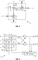
- FIG 3 is a block diagram of an example 2x4 90° hybrid 240, where I 1 and I 2 denote the two inputs and O 1 - O 4 denote the four outputs.
- O 1 and O 2 represent one of the two differential pairs that are detected in the front-end 200 shown in Figure 2 , while O 3 and O 4 make up the other.
- HWP 310 is a half-wave plate
- QWP 320 is a quarter-wave plate
- PBS 330 is a polarization beam splitter.
- the receiver Because the received polarization-division multiplexed optical signal has two independent information streams impressed on its orthogonal polarizations by intensity modulation at the transmitter, the receiver has to split the received signal into two orthogonal polarizations to retrieve the information. Since the information is imprinted on the intensities of the X and Y components of the transmitted signal E t , the only parameters needed at the receiver to retrieve the information are estimates of the Stokes parameters E 0 t and E 1 t , which are the sum and difference, respectively, of the transmitted intensities
- 2 the only parameters needed at the receiver to retrieve the information are estimates of the Stokes parameters E 0 t and E 1 t , which are the sum and difference, respectively, of the transmitted intensities
- an estimate E ⁇ 0 t can be recovered by simply summing the detected intensities
- E ⁇ 1 t of the Stokes parameter E 1 t requires additional processing, however, because of the polarization rotation imposed on the optical signal between the optical transmitter and optical receiver.
- This additional processing can be performed with a digital signal processor (DSP) implementing a multiple-input single-output (MISO) filter acting upon the Stokes parameters of the received field, namely, E 1 r E 2 r , and E 3 r .
- DSP digital signal processor
- MISO multiple-input single-output
- ⁇ is an adaptation step size
- E k r represents an N -tap input vector corresponding to the k th received Stokes parameter.
- the single polarization modulated signal was then amplified using a ThorlabsTM 1310-nm polarization-sensitive booster optical amplifier (BOA) and then fed to a polarization-division-multiplexing (PDM) emulator to generate a PDM intensity-modulated (IM) signal.
- BOA ThorlabsTM 1310-nm polarization-sensitive booster optical amplifier
- PDM polarization-division-multiplexing
- the decorrelation delay of the emulator between the two orthogonal SOPs should correspond to an integer number of symbols at the baud rate of operation. Also, the delay should be sufficiently small ( ⁇ 150 ps) to ensure that the laser phases at both transmitted polarizations are approximately the same, in order for the DSP to function reliably.
- the two optical paths from the polarizing beam spliter (PBS) to the polarization beam combiner (PBC) can be matched to guarantee the same laser phase on both polarizations.
- the signal was, in respective tests, launched into either 0, 2, 10 or 20 km of ComingTM SMF-28e + optical fiber.
- the front-end was followed by six single-ended PicometrixTM receivers, each comprising a p-type/intrinsic/n-type (PIN) photodiode followed by a transimpedance amplifier (TIA), to detect the Stokes parameters.
- PIN p-type/intrinsic/n-type
- TIA transimpedance amplifier
- the signals were then sampled by two AgilentTM Q-series real-time oscilloscopes at 80-GSamples/s, with the samples being stored for offline processing.
- the signal can of course be processed immediately, without storing, for example using an application specific integrated circuit (ASIC) that performs the DSP operations described above in real time, on digital samples obtained by sampling the analog signals at the outputs of the six receivers using analog-to-digital converters(ADCs).
- ASIC application specific integrated circuit
- FIG. 5 illustrates an example optical transmitter 500 employed in this modified system.
- the transmitter 500 of Figure 5 comprises a laser 110, a polarization beam splitter 120, and a pair of intensity modulators (IMs) 130, in parallel branches.
- the two branches are polarization combined, with polarization beam combiner 140.
- one of the branches in optical transmitter 500 also comprises an optical phase modulator (PM) 510.
- the transmitter externally intensity modulates a single laser, by impressing two independent information streams on each of two orthogonal states of polarization (SOPs) of the signal originating from a single laser.
- One of the intensity modulators is followed (or preceded) by the phase modulator, which modulates the phase difference between the two orthogonal SOPs, using a third independent information stream, before the SOPs are combined. This allows for modulation over three degrees of freedom.
- the time-varying Jones vector is
- the last two elements of the estimated derotated power vector i.e., S ⁇ 2 t and S ⁇ 3 t
- the optical signal produced by transmitter 500 has two independent information streams impressed on its orthogonal polarizations by intensity modulation at the transmitter.
- the receiver has to split the received signal into two orthogonal polarizations to retrieve the information.
- the principal axes of the receiver PBS are not necessarily aligned with that of the PBC of the transmitter, which means that
- 2 is not likely to be equal to
- E x t includes an inter-polarization phase-modulation component that is manifested in the received components E x r and E y r ; an estimate of this phase component needs to be recovered, in addition to estimates of the transmitted intensities
- the second stage in the DSP stack shown in Figure 6 comprises four single-input single-output (SISO) FIR filters 620, which are used to remove any residual ISI uncompensated by the first stage, and mainly residual transmitter-side ISI.
- SISO single-input single-output
- FIG. 7 A more detailed schematic diagram of an example transmitter assembled for demonstration purposes is shown in Figure 7 , while Figure 8 shows a detailed schematic diagram of a corresponding receiver.
- a 14.3-dBm laser diode (LD) at 1550 nm is intensity modulated at the transmitter by a 41-GHz silicon photonic modulator.
- a radio-frequency (RF) amplifier amplifies a 70-GSamples/s information signal from an 8-bit digital-to-analog converter (DAC) channel.
- DAC digital-to-analog converter
- the transmitter DSP for generating the IM can be that reported previously in M. Chagnon, et al., Opt. Exp. vol. 22, no.17, 2014 . Similar processing can be applied to the PM signal, without the MZM arcsin compensation. It should be appreciated that several of the components used in the transmitter of Figure 5 (e.g., the EDFA, filter, PCs), which is suitable for experimental purposes, would not be required when realizing a fully integrated transmitter as shown in Figure 5 .
- each of the four photoreceivers/detectors has its own frequency response that induces inter-symbol interference on the received power vectors.
- ISI increases, there is be an increased penalty associated with using a small number of taps in the first derotation stage, as the second stage SISOs are not able to cancel residual cross talk from other channels.
- receiver that includes a DSP algorithm that recovers, simultaneously, the information on the multiple intensities imprinted by the transmitter on each polarization and, in some embodiments, the information from the multi-level inter-polarization phase modulation.
- an example transmitter includes a laser and a polarizing beam splitter coupled to the output of the laser to produce first and second optical signals having first and second polarizations, respectively. These polarizations may be at least substantially orthogonal, in some embodiments.
- First and second intensity modulators are configured to impress multi-level intensity modulation on the first and second polarizations, respectively, based on first and second multi-level modulation signals derived from respective first and second information streams.
- a phase modulator further impresses a multi-level phase modulation on the intensity-modulated output of the first intensity modulator, using a multi-level phase modulation signal derived from a third information stream. The output from the second intensity modulator and the output from the phase modulator are combined, using a phase maintaining combiner, for transmission.
- the digital signal processing circuit performs polarization demultiplexing of the orthogonal intensity-modulation, and demodulates the intensity modulation signal from each polarization, to recover first and second information signals used to impress the intensity modulation on the orthogonal polarizations.
- the digital signal processing circuit implements a 4x4 multiple-input multiple-output (MIMO) filter that inverts the polarization rotation imposed on the signal between the transmitter and receiver.
- MIMO multiple-input multiple-output
- this MIMO filter further mitigates receiver-side inter-symbol interference (ISI).
- ISI receiver-side inter-symbol interference
- four error signals are evaluated, based on the difference between desired equalizer outputs and the four current outputs. The error signals are used to update the taps of all 16 FIR filters of the 4x4 MIMO, using their respective inputs, which are updated using the stochastic gradient descent algorithm.
- the equalizer so formed is initially updated using training symbols before switching to a decision-directed mode, from which information-carrying symbols are produced.
- the digital signal processing circuit further implements four single-input single-output (SISO) FIR filters, which operate on the outputs from the 4x4 MIMO filter to remove any residual ISI uncompensated by the first stage and residual transmitter-side ISI. Estimates of the three information streams are obtained from the outputs of these SISO FIR filters, in these embodiments.
- SISO single-input single-output
- Figures 11 and 12 illustrate process flow diagrams corresponding to example methods carried out in embodiments of the transmitter and receiver described above.
- the method illustrated in Figure 11 includes, as shown at block 1110, impressing a first intensity modulation on a first optical signal, to obtain a first intensity-modulated signal, wherein the first intensity modulation is based on a first modulation signal derived from a first stream of information bits.
- the method further includes, as shown at block 1120, impressing a second intensity modulation on a second optical signal, to obtain a second intensity-modulated signal, wherein the second intensity modulation is based on a second modulation signal derived from a second stream of information bits.
- the method further includes impressing a multi-level phase modulation on the first intensity-modulated signal, to obtain an intensity-modulated and inter-polarization-phase-modulated signal.
- the polarization of the first optical signal or the second optical signal is rotated. Note that this rotation may be performed before or after the impressing of the intensity modulation, in various embodiments.
- the intensity-modulated and inter-polarization-phase-modulated signal and the second intensity-modulated signal are combined, and the combined signal is transmitted via an optical fiber.
- the rotating of the polarization of the first optical signal or the second optical signal is performed in such a way that the intensity-modulated and inter-polarization-phase-modulated signal and the second intensity-modulated signal, as combined and transmitted, have first and second optical states of optical polarization. These first and second states of optical polarization are preferably at least substantially orthogonal.
- the method illustrated in Figure 12 includes, as shown at block 1210, receiving an intensity-modulated, polarization-division multiplexed optical signal with inter-polarization modulation.
- the method further includes detecting a time-varying intensity for each of first and second orthogonal polarizations of the received optical signal, as shown at block 1220.
- the detected intensities for the first and second orthogonal polarizations of the received optical signal and the signal components S 2 and S 3 are de-rotated.
- First and second information bit streams are detected from the de-rotated first and second orthogonal polarizations of the received optical signal, as shown at block 1250, and a third information bit stream is demodulated from the angle of the sum of signal components S 2 and jS 3 , as shown at block 1260. It will be appreciated that the variations and/or additional details provided above in the detailed description of Figures 1-8 are equally applicable to the methods illustrated in Figures 11 and 12 .
Landscapes
- Engineering & Computer Science (AREA)
- Computer Networks & Wireless Communication (AREA)
- Signal Processing (AREA)
- Physics & Mathematics (AREA)
- Electromagnetism (AREA)
- Optical Communication System (AREA)
Description
- The present application relates generally to optical transmitters and receivers, and more particularly relates to optical transmitter and receiver devices using polarization multiplexing.
- Optical interconnects for short reach applications such as intra-data center information transport need to support more data throughput. Approaches should be cost effective, energy efficient, and require a small footprint. To meet these requirements, the use of a single-laser transmitter and a receiver having a passive optical receiver front-end and using direct detection should be employed.
- With the recent standardization of 100 Gigabit/second (Gbps) Ethernet, it is generally agreed that achieving 100 Gbps and beyond on a single wavelength channel is mandatory to realize the envisioned 400 Gbps and 1 Terabit per second (Tbps) targets. Modulating a single laser provides a more scalable and cost effective solution than counterparts that involve the use of multiple wavelengths or multiple fiber lanes.
- Demonstrations of 100 Gbps per wavelength have been reported for short-range transmissions, using various modulation formats. Some experiments employed polarization-division multiplexing (PDM) to halve the desired baud rate, i.e., the number of symbols per second, to reach 100 Gbps, with the polarization demultiplexing done optically, with a polarization controller/stabilizer.
- Examples of these reported techniques include the use of four-level pulse-amplitude modulation (PAM-4) with PDM, as reported by R. Rodes, et al., "100 Gb/s single VCSEL data transmission link," in 2012 Optical Fiber Communication Conference (OFC 2012), paper PDP5D.10, 2012. Other examples include an approach based on half-cycle Nyquist subcarrier PDM with 16-QAM, reported by A. Karar, et al., ECOC, paper PDP Th.3.A.4, 2012, and another based on multi-band CAP, reported by M. I. Olmedo, et al., in J. Lightwave Technol., vol. 32, no. 4, 2014. Still another example uses discrete multi-tone (DMT), as reported by W. Yan, et al., OFC, paper OM3H.1, 2013. PDM was also used in a self-coherent system experiment reported by D. Che, et al., in Opt. Lett., vol. 39, no. 11, 2014. 112-Gbps PAM transmission was reported by the present inventors in M. Chagnon, et al., Opt. Exp. vol. 22, no.17, 2014, and extended to include PDM for 224 Gbps over 10 kilometers (km), in M. Morsy-Osman, et al., ECOC 2014, Paper PD.4.4.
-
US 2011/044702 A1 discloses an optical splitter that splits the continuous wave light generated by a light source and guides the light to first and second modulators. The first modulator generates a modulated optical signal H by modulating the input light according todata 1. Likewise, the second modulator generates a modulated optical signal V by modulating the input light according todata 2. Each of the modulators comprises a Mach-Zehnder interferometer. The Mach-Zehnder interferometer equally splits the already splitted continuous wave light emitted by the light source and guides it to optical paths P1 and P2. Then, the phase difference between the optical paths P1 and P2 is controlled to a specified target value or to the value shifted from the target value by π using a phase shifter. Subsequently, the light of the optical paths P1 and P2 is recombined, and a polarization beam combiner generates a polarization multiplexed optical signal by combining the modulated optical signals V and H.
The article "Compensation for In-Phase/Quadrature Imbalance in Coherent-Receiver Front End for Optical Quadrature Amplitude Modulation" (Md. Saifuddin Faruk et al., IEEE PHOTONOCS JOURNAL, IEEE, USA, vol. 5, no.2, 1 April 2013) deals with a coherent optical front-end receiver which is configured to receive a dual-polarization quadrature-amplitude-modulation signal and to compensate for imbalance between the IQ channels of the quadrature-amplitude-modulation signal. - Despite these reported techniques, there still remains a need for cost-effective systems that transmit at data rates well beyond 100 Gbps, on a single wavelength.
- The invention is solely defined by the appended claims. Embodiments not fully falling within the scope of the appended claims are to be understood merely as examples useful for understanding the invention.
- A first aspect of the techniques and apparatus disclosed herein is directed to an optical transmitter according to
claim 1. - A second aspect of the techniques and apparatus disclosed herein is directed to an optical receiver according to
claim 4. - A third aspect of the presently disclosed techniques and apparatus is directed to a method of generating a modulated optical signal according to claim 9.
A fourth aspect of the presently disclosed techniques and apparatus is directed to a method according to claim 15. Other embodiments are detailed in the dependent claims. - Those of ordinary skill in the art will recognize additional features and advantages of the disclosed techniques and apparatus upon reading the following detailed description, and upon viewing the accompanying drawings.
-
-
Figure 1 illustrates an example optical polarization-division multiplexing transmitter. -
Figure 2 illustrates an example optical front-end. -
Figure 3 illustrates a 90° hybrid, as used in the optical front-end ofFigure 2 . -
Figure 4 illustrates an example digital signal processing stack for use in an optical receiver. -
Figure 5 illustrates another example optical polarization-division multiplexing transmitter, where intensities on each polarization and the inter-polarization phase can each be modulated. -
Figure 6 illustrates details of another example digital signal processing stack, according to some embodiments. -
Figure 7 illustrates an experimental transmitter setup. -
Figure 8 illustrates an experimental receiver setup. -
Figures 9A, 9B, and 9C illustrate performance measurements of a system according to an embodiment. -
Figure 10 illustrates measured eye diagrams obtained from an example system. -
Figure 11 is a process flow diagram illustrating an example method according to some embodiments of the described techniques. -
Figure 12 is a process flow diagram illustrating another example method according to some embodiments of the described techniques. - Various features of the invention will now be described with reference to the figures. These various aspects are described hereafter in greater detail in connection with exemplary embodiments and examples to facilitate an understanding of the invention, but should not be construed as limited to these embodiments. Rather, these embodiments are provided so that the disclosure will be thorough and complete, and will fully convey the scope of the invention to those skilled in the art.
- Aspects of the invention may be described below in terms of sequences of actions or functions to be performed by elements of a computer system or other hardware capable of executing programmed instructions. It will be recognized that the various actions could be performed by specialized circuits, by program instructions being executed by one or more processors, or by a combination of both.
- In some alternate implementations, the functions/acts may occur out of the order noted in the sequence of actions.
- Several of the embodiments described herein concern optical transmitters and receivers that use intensity modulation and polarization multiplexing, with a direct-detection approach employed in the receivers. Some of the embodiments also exploit inter-polarization phase modulation. The optical receivers described herein include a multiple-input and multiple-output (MIMO) digital signal processor (DSP) algorithm operating in the Stokes space, following a direct-detection receiver front-end. Modulating the intensity of the two orthogonal polarization states of a single laser enables either doubling the maximum achievable bit rate on a single wavelength channel or halving the required baud rate (and consequently the bandwidth of electronic components) to achieve a given bit rate on a single wavelength. Adding the inter-polarization modulation allows the maximum achievable bit rate on the single wavelength channel to be increased even further (or the required baud rate to achieve a certain baud rate to be reduced even further).
- For the sake of clarity, we define polarization as a property of the electromagnetic light wave, which describes the direction of oscillation of the electric field associated with the electromagnetic wave. Two orthogonal polarizations states result, for example, from applying an optical signal, rotated by 45 degrees, to a polarizing beam splitter (PBS), which provides at its two outputs two electromagnetic waves having their electric fields oscillating at perpendicular directions. Alternatively, two orthogonal polarization states may be produced by first splitting an optical signal carried in a polarization-maintaining fiber (PM fiber) with a polarization-maintaining optical beam splitter. One of the two output branches then receives a 90-degree polarization rotation, e.g., using a polarization controller, before the signals on the two branches are orthogonally combined by a polarization beam combiner.
-
Figure 1 is a block diagram illustrating components of an exampleoptical transmitter 100, employing polarization-division multiplexing (PDM). Such a transmitter is described in M. Morsy-Osman, M. Chagnon, M. Poulin, S. Lessard, D.V. Plant, "1λ × 224 Gb/s 10 km Transmission of Polarization Division Multiplexed PAM-4 Signals Using 1.3 µm SiP Intensity Modulator and a Direct-Detection MIMO-based Receiver," in Proc. of ECOC, Paper PD.4.4, Sept. 2014. -
Optical transmitter 100 comprises a single-wavelength laser diode 110, the output of which is coupled to anoptical beam splitter 120, in this case illustrated as a polarizing beam splitter.Optical beam splitter 120 has first and second outputs, producing first and second states of polarization, respectively, of the optical carrier generated bylaser diode 110. These first and second states of polarization are orthogonal or substantially orthogonal to one another. - The first and second outputs of
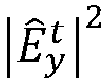
optical beam splitter 120 are coupled to first and secondoptical intensity modulators 130, respectively. The first and second optical intensity modulators are independently driven by first and second drive signals (not shown) derived from first and second information streams, respectively, according to any amplitude-based modulation scheme, such as the multi-level pulse-amplitude modulation (PAM) schemes discussed above. The intensity-modulated outputs of the first and secondoptical intensity modulators 130 are combined withoptical beam combiner 140. The output ofoptical beam combiner 140 thus comprises a polarization-division multiplexed optical signal that comprises intensity modulated signals on each polarization, as produced by the first and secondoptical intensity modulators 130. - The transmitted optical signal can be also called the transmitted field. The word "field" is used interchangeably with the word "signal" in the context of this description. Transmitted field refers to the light field or, more specifically, the electrical field of the electromagnetic light wave. The field can be denoted by E, to distinguish it from the intensity of the field, which is |E|2. The field has both magnitude and phase (complex), whereas the intensity is the squared magnitude of the field.
- The transmitted signal can be equivalently represented by a Jones vector


- Propagation through a fiber channel results in a transmission impairment for the signal called polarization rotation, which can be mathematically modeled as a unitary transformation. This unitary transformation can be mathematically modeled by either a 2x2 complex-valued matrix J or a 3x3 real-valued matrix R . In the Stokes space, this transformation is expressed as


- Generally, then, the transmitted and received fields can thus be represented by 4D power vectors in the form [|Ex |2,|Ey |2,S 2,S 3] T , where


-
Figure 2 illustrates elements of a receiver front-end 200, which is arranged to detect the components of the 4D received power vector
end 200 comprises a polarizing beam splitter (PBS) 210 having an input that, during operation, is coupled to a single-mode optical fiber linking the receiver to theoptical transmitter 100.Polarization beam splitter 210 splits the received optical signal into two signals with orthogonal polarizations, i.e., two electromagnetic waves having their electric fields oscillating at perpendicular directions. The two outputs of polarization beam splitter are each coupled to an optical coupler 220 (e.g., a 50/50 or 90/10 coupler) - in the illustrated example, thesecouplers 220 are polarization-maintaining devices, in that they do not impact the relative polarizations of their outputs. One output from each of thecouplers 220 is directly detected, withdetectors 250, to obtain the signal components

Figures 2 and throughout the present discussion, for simplicity. The other output from eachcoupler 220 is supplied to a 2x4 90°hybrid 240, after the output from one coupler is polarization-rotated by 90° byrotator 230. These inputs to the 2x4 90°hybrid 240 are beat against each other to provide differential outputs, as illustrated inFigure 2 and as explained in further detail below. The differential outputs from the 2x4 90°hybrid 240 are detected, withdetectors 260, to obtain the signal components

-
Figure 3 is a block diagram of an example 2x4 90°hybrid 240, where I1 and I2 denote the two inputs and O1 -O4 denote the four outputs. O1 and O2 represent one of the two differential pairs that are detected in the front-end 200 shown inFigure 2 , while O3 and O4 make up the other. In the illustration,HWP 310 is a half-wave plate,QWP 320 is a quarter-wave plate, andPBS 330 is a polarization beam splitter. The outputs of the 90°hybrid correspond to I1 +I2 , I1 +jI2 , I1 -I2, and I1 +jI2 , where j=sqrt(-1). - In a link comprising the
optical transmitter 100 shown inFigure 1 and the optical receiver front-end 200 shown inFigure 2 , information is carried on the time-varying intensities of the X and Y components of the transmitted signal, i.e.,

- Because the received polarization-division multiplexed optical signal has two independent information streams impressed on its orthogonal polarizations by intensity modulation at the transmitter, the receiver has to split the received signal into two orthogonal polarizations to retrieve the information. Since the information is imprinted on the intensities of the X and Y components of the transmitted signal Et , the only parameters needed at the receiver to retrieve the information are estimates of the Stokes parameters


end 200 are not likely to be aligned with those of the transmitter, which means that


polarization beam splitter 210 in the optical front-end 200 shown inFigure 2 resolves the received optical signal into two orthogonal components, it does so without any reference to the coordinate system of the optical transmitter. This is analogous to finding the x and y components of a vector where the coordinate system of the receiver may be different from the original coordinate system. - Since


end 200 ofFigure 2 , to obtain the 0th Stokes parameter


- Obtaining an estimate


end 200 ofFigure 2 (again, ignoring any scaling factor). The Stokes parameter


-
Figure 4 is a block diagram illustrating the operations carried out by an example DSP, according to some examples of the presently disclosed techniques. This DSP performs the polarization demultiplexing, correcting for the unknown polarization rotation of the received optical signal, and recovers the originally transmitted information from the demultiplexed modulation signals. - As seen in
Figure 4 , the DSP implements a SISO Finite Impulse Response (FIR)filter 410, and a3x1 MISO filter 420.FIR filter linear filters 425 in3x1 MISO filter 420 are summed, to provide a single output. The combination ofFIR filter 410 and3x1 MISO filter 420 might also be referred to as a MIMO filter, since it has four inputs (the Stokes parameters) and two outputs. -
FIR filter 410 filters the 0th Stokes parameters


end 200. - The lower part of the DSP stack shown in
Figure 4 is a 3x1 multiple-input single-output (MISO) bank of FIR filters 425, with tap weight vectors h11 , h21 , and h31 , each having N real-valued taps, the FIR filters 425 accepting the Stokes parameters


MIMO filter 420 would not perform ISI mitigation. - As seen in
Figure 4 , estimates


FIR filter 410 and3x1 MIMO filter 420. These recovered estimates are proportional to the modulation signals applied to the orthogonal states of polarization in the optical transmitter, so the original information streams can be recovered directly from these estimates. - The real-valued tap weight vectors h00 , h11 , h21 , and h31 can be adapted, e.g., using Least-Means Square (LMS) algorithm. This adaptation effectively corrects and tracks the alignment between the reference polarization axes in the optical transmitter and optical receiver, while simultaneously mitigating inter-symbol interference. In
Figure 4 , this is shown at error calculation and tapupdate function 430, which may be implemented with an algorithm executed by digital signal processing circuitry. This algorithm updates the taps h00 , h11 , h21 , and h31 of1x1 FIR filter 410 and3x1 MIMO filter 420, based on two error signals calculated from the estimates


- The error signals ex and ey are used to update the tap weights for the (i + 1) th symbol based on the error signals and the tap weights at the ith symbols, using the least-mean-squares (LMS) algorithm as follows:



- In an experimental setup (not illustrated), a 20-milliwatt (mW) 1310-nm NEL™ distributed feedback (DFB) laser was externally modulated by a packaged system-in-package (SiP) intensity modulator. A differential radio frequency (RF) signal was generated from a 70-Gigasamples/second (GSa/s) 8-bit digital-to-analog converter (DAC) and amplified using an Inphi™ linear driver. The output of the Inphi linear driver is applied to the SiP modulator, which was constantly operated at the quadrature point of the optical power-transfer function. The single polarization modulated signal was then amplified using a Thorlabs™ 1310-nm polarization-sensitive booster optical amplifier (BOA) and then fed to a polarization-division-multiplexing (PDM) emulator to generate a PDM intensity-modulated (IM) signal.
- The decorrelation delay of the emulator between the two orthogonal SOPs should correspond to an integer number of symbols at the baud rate of operation. Also, the delay should be sufficiently small (<150 ps) to ensure that the laser phases at both transmitted polarizations are approximately the same, in order for the DSP to function reliably. In a true PDM IM transmitter, where two separate modulators are available and no emulation is needed, the two optical paths from the polarizing beam spliter (PBS) to the polarization beam combiner (PBC) can be matched to guarantee the same laser phase on both polarizations.
- Next, the signal in the experimental setup was filtered, using a 1-nm optical filter to reject the out-of-band noise from the BOA. It is noteworthy that the combination of the BOA and the filter were used to counteract some of the insertion loss (IL) of the optical components, such as the SiP modulator (IL∼ 14decibel (dB) at maximum transmission), the PDM emulator (IL∼4dB), and the receiver front-end (IL∼7dB from the PBS input to either one of the detectors that measure


- Next, the signal was, in respective tests, launched into either 0, 2, 10 or 20 km of Coming™ SMF-28e + optical fiber. At the receiver, the front-end was followed by six single-ended Picometrix™ receivers, each comprising a p-type/intrinsic/n-type (PIN) photodiode followed by a transimpedance amplifier (TIA), to detect the Stokes parameters. In the experimental setup, this was done instead of using balanced photodetectors. The signals were then sampled by two Agilent™ Q-series real-time oscilloscopes at 80-GSamples/s, with the samples being stored for offline processing.
- In a live embodiment, the signal can of course be processed immediately, without storing, for example using an application specific integrated circuit (ASIC) that performs the DSP operations described above in real time, on digital samples obtained by sampling the analog signals at the outputs of the six receivers using analog-to-digital converters(ADCs).
- Regarding the digital signal processing employed, the transmitter side DSP includes pulse shaping, pre-compensation of the limited frequency response of all transmitter side components, and pre-compensation of the nonlinear optical transfer function of the modulator. In the experimental setup, the transmitted samples were prepared offline after applying this transmitter-side processing, and then loaded to the memory of the DACs that fed the intensity modulator. In a live embodiment, the transmitted bits can be processed in real-time, e.g., again using an ASIC that executes the DSP operations and feeds the samples to the DACs in a real-time fashion.
- In the experimental embodiment, at the receiver side, offline processing started by subtracting waveforms captured at the balanced output pairs of the 2x4 hybrid to eliminate the direct detection terms and obtain


- BERs for both PDM and single polarization PAM-4 signals were compared to one another, for both the 0 and 20 km fiber scenarios, to verify the penalty of PDM compared to single polarization transmission (i.e., where one branch of emulator is disconnected) operating at the same baud rate, i.e. half the bit rate. It was observed that there is no penalty at high baud rates whereas there was a slight increasing penalty as the baud rate decreases. This is due to the saturation of the TIAs which impacts the PDM system especially when the polarization angle mismatch between the transmitter and receiver is closer to 45°. In this experimental setup, reducing the received power potentially avoids the TIA saturation problem but also increases the impact of receiver thermal noise.
- The results obtained from the experimental setup clearly show that the optical transmitter and receiver configurations described above enable the doubling of the maximum achievable bit rate, compared to single polarization transmission, and enable 112 Gb/s using either PAM-2 or PAM-4, with very low BERs (10-5∼ 10-6), if operated close to the optimum received power, which reduces the forward error correction (FEC) overhead requirement dramatically and hence reducing the power consumption of the transceiver's integrated circuits (ASICs) compared to a single polarization system that delivers 112 Gb/s. With the potential improvements of the coupling losses of the SiP modulator as well as the prospect of integrating all the discrete optical components at the receiver front-end on the same SiP chip, the losses are expected to decrease and enable the power budget with no optical amplifier.
- The discussion above provided details of an optical transmitter and receiver that operated using polarization multiplexing of two intensity-modulated orthogonal states of polarization. Further improvements in throughput are obtained by adding inter-polarization phase modulation to the system. This modified system includes an optical transmitter that is augmented with a phase modulator in one branch of the optical transmitter, with the phase modulator driven by a modulation signal corresponding to a third information stream. The optical receiver includes a multiple-input multiple-output (MIMO) digital signal processing algorithm operating in the Stokes space, following a direct-detection optical front-end that can be identical to the one illustrated in
Figure 2 and described above. As shown above, the intensity modulation of the two orthogonal polarization states of a single laser enables either doubling the maximum achievable bit rate on a single wavelength channel or halving the required baud rate (and consequently the bandwidth of electronic components) to achieve a given bit rate on a single wavelength. Adding the inter-polarization phase modulation, as described in further detail below allows the maximum achievable bit rate on the single wavelength channel to be increased even further (or the required baud rate to achieve a certain baud rate to be reduced even further). -
Figure 5 illustrates an exampleoptical transmitter 500 employed in this modified system. As was the case in the optical transmitter shown inFigure 1 , thetransmitter 500 ofFigure 5 comprises alaser 110, apolarization beam splitter 120, and a pair of intensity modulators (IMs) 130, in parallel branches. The two branches are polarization combined, withpolarization beam combiner 140. Unlike the transmitter shown inFigure 1 , however, one of the branches inoptical transmitter 500 also comprises an optical phase modulator (PM) 510. Thus, the transmitter externally intensity modulates a single laser, by impressing two independent information streams on each of two orthogonal states of polarization (SOPs) of the signal originating from a single laser. One of the intensity modulators is followed (or preceded) by the phase modulator, which modulates the phase difference between the two orthogonal SOPs, using a third independent information stream, before the SOPs are combined. This allows for modulation over three degrees of freedom. - In the transmitter shown in
Figure 1 , the time-varying Jones vector is


- As was the case with the polarization-division multiplexed intensity-modulated signal produced by the optical transmitter of
Figure 1 , the optical signal produced bytransmitter 500 has two independent information streams impressed on its orthogonal polarizations by intensity modulation at the transmitter. Thus, the receiver has to split the received signal into two orthogonal polarizations to retrieve the information. Again, of course, the principal axes of the receiver PBS are not necessarily aligned with that of the PBC of the transmitter, which means that


- As detailed below, this alignment can be corrected through an algorithm to update the taps of the MIMO filter, where the algorithm receives error signals, evaluated using an error calculator as explained below, the current tap values, and the current tap input vectors as inputs. For each received symbol, the updated tap values to be used for the next symbol are calculated with a least-means-square algorithm, thus minimizing the error signals, as explained below. A digital signal processing algorithm can then retrieve the transmitted intensities from the received ones. The digital signal processing algorithm can also retrieve the 4-level inter-polarization phase modulation impressed on the transmitted signal by recovering the phase between the polarizations, using the signal components


- An optical receiver for recovering the three information streams from the optical signal produced by
optical transmitter 500 can comprise an optical front-end identical to that shown inFigure 2 , as described in detail above. This receiver front-end 200 is arranged to detect the components of the 4D received power vector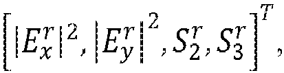


Figure 5 ,


- An optical receiver for recovering the three information streams from the optical signal produced by
optical transmitter 500 thus further comprises a digital signal processing circuit configured to carry out the digitalsignal processing stack 600 shown inFigure 6 . Digitalsignal processing stack 600 performs the polarization demultiplexing, correcting for (i.e., inverting) the unknown the polarization rotation imposed on the signal between the transmitter and receiver, and recovers the originally transmitted information from the demultiplexed modulation signals. In some embodiments, the DSP further mitigates receiver-side inter-symbol interference (ISI). - The first stage of the DSP stack is a 4x4 multiple-input multiple-output (MIMO)
filter 610, which inverts the polarization rotation and mitigates mainly receiver-side inter-symbol interference (ISI). Four error signals are evaluated, based on the difference between the desired equalizer outputs and the four current outputs, in a manner corresponding to that described above in connection withFigure 4 . The error signals are used to update the taps of all 16 FIR filters of the 4×4MIMO filter 610, using their respective inputs, which are updated using the stochastic gradient descent algorithm. More specifically, the equalizer is initially updated using training symbols before switching to a decision-directed mode. The second stage in the DSP stack shown inFigure 6 comprises four single-input single-output (SISO) FIR filters 620, which are used to remove any residual ISI uncompensated by the first stage, and mainly residual transmitter-side ISI. Finally, estimates of the three information streams are obtained, corresponding to

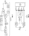
- A more detailed schematic diagram of an example transmitter assembled for demonstration purposes is shown in
Figure 7 , whileFigure 8 shows a detailed schematic diagram of a corresponding receiver. In the example setup shown inFigure 7 , a 14.3-dBm laser diode (LD) at 1550 nm is intensity modulated at the transmitter by a 41-GHz silicon photonic modulator. A radio-frequency (RF) amplifier amplifies a 70-GSamples/s information signal from an 8-bit digital-to-analog converter (DAC) channel. The single polarization intensity modulated (IM) light from the modulator, at about -4 dBm, is amplified by an erbium-doped fiber amplifier (EDFA) and filtered by a 0.8 nanometer tunable filter to remove out-of-band noise. A polarization controller PC1 aligns the SOP to the axis of a polarization-maintaining splitter before entering the dual polarization emulator. One output port is phase modulated by a low-Vπ LiNbO3 phase modulator that is driven by another amplified DAC channel, which thus allows modulating a phase difference between the two orthogonal IM signals. The other output port is delayed by a variable optical delay line VODL2, allowing recombination at the polarization beam combiner (PBC) with the desired optical path difference. An optical on-off switch and two polarization controllers PC1 and PC2 allow for comparing and equating the power on each polarization after the PBC. Before the emulator, a variable optical delay line VODL1 delays the IM waveform such that the PM waveform is applied at the proper time on the IM field. - The transmitter DSP for generating the IM can be that reported previously in M. Chagnon, et al., Opt. Exp. vol. 22, no.17, 2014. Similar processing can be applied to the PM signal, without the MZM arcsin compensation. It should be appreciated that several of the components used in the transmitter of
Figure 5 (e.g., the EDFA, filter, PCs), which is suitable for experimental purposes, would not be required when realizing a fully integrated transmitter as shown inFigure 5 . - The receiver in
Figure 8 comprises a polarization beam splitter (PBS) that separates the received signal on two fixed orthogonal polarization axes, followed by two 90/10 couplers. The 10% ports of each coupler go to two photoreceivers, each comprising a PIN photodiode and a transimpedance amplifier (TIA), generating

Figure 8 , because the two balanced photodetectors (BPDs) following the hybrid do not have TIAs. Optical time alignment is assured prior to entering the 90° optical hybrid, using variable optical delay line VODL3 and polarization controllers PC5 and PC6. The two balanced photodetectors generate the receiver signal components

Figure 6 . Finally, hard decisions are performed for the received symbols; in the experimental setup, a bit-error-rate (BER) is calculated to evaluate the performance of the setup. In a live embodiment, the signal can of course be processed immediately, without storing, using, for example, an application-specific integrated circuit (ASIC) that performs real-time DSP operations on the digital samples obtained by sampling the analog signals at the outputs of the photodetectors. -
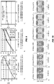
Figures 9A, 9B, and 9C illustrate BER performance for the experimental setup shown inFigures 7 and 8 , over varying bit rates and SOPs. ForFigure 9A , the symbol rate of the 6 bits/symbol DP-PAM4+4PM format is varied from 28 Gbaud to 58.4 Gbaud, and information is recovered using the DSP presented above. BERs below the HD-FEC threshold are obtained up to ≈ 300 Gbps, while a BER of 1.6×10⁻² is obtained at a throughput of 350 Gbps, below the SD-FEC threshold. Crosses at 280 Gbps and 350 Gbps are added to the figure, as those bitrates represent 250 Gbps and 280 Gbps of data payload below HD and SD-FEC with respective overheads of 12% and 25%. -
Figure 9B shows the performance degradation on the intensity modulation when phase modulation is enabled, for both single polarization (SP) and dual polarization (DP), using the MEMS on-off switch. As all possible transmission configurations are presented, namely SP or DP with PM on or off, the DSP stack presented for the full DP-PAM4+4PM format cannot be applied. In order to de-embed the SOP rotation penalty from the application of PM, the SOP is aligned to the receiver's axes, and regular PAM4 IM/DD DSP is used, as reported in M. Chagnon, et al., Opt. Exp. vol. 22, no.17, 2014, on available IM signals present on the receiver.Figure 9B shows the strong deterioration of the intensity modulated signals, on both orthogonal polarizations, even if PM is applied to only one polarization axis. At 42 Gbaud, turning the PM on increases the BER 50-fold, while at 56 Gbaud it increases from ≈ 10-3 to 8×10⁻³. The deterioration of the IM signal due to PM is because of the undesired amplitude modulation components that arise from generating the optical phase modulated signal. The larger deterioration at lower symbol rates is due to the larger available RF swing on the PM with decreasing symbol rates. -
Figure 9C presents the BER of the DP-PAM4+4PM format at 56 Gbaud, as the received SOP is varied from 0° to 45° and processed with the MIMO/SISO receiver DSP. The rising BER with increasing rotation angle=arcsin(|b)| from 0° to 45° occurs because the received signal power on the two PIN+TIA detectors increases as the cross term 2Re{ab*} in


- Finally,
Figure 10 shows the eye diagrams of the IM PAM4 on the x and y states of polarization and the four phases of the inter-polarization phase modulation, at 28 and 56 Gbaud. - It should be noted that at 1550 nm, the demonstration wavelength, propagation of signals with this modulation format over short distances was not feasible because of the inherent interplay between phase modulation and chromatic dispersion (CD). It is known that chromatic dispersion converts phase modulation to intensity modulation. This CD-PM interplay would be strongly minimized by operating around 1310 nm which, as per IEEE Std 802.3ba, is the defined operating wavelength for short reach optics.
- As indicated by the example performance results shown in
Figures 9 and 10 , a polarization-multiplexed intensity with inter-polarization phase modulation transceiver using direct-detection has been demonstrated at 280 and 350 Gbps, below the HD and SD-FEC thresholds, on a single wavelength. A novel two-stage 4-by-4 MIMO / SISO receiver DSP operating on the 4D power space after a direct detection receiver was presented and employed for derotation and symbol recovery. All components of the transmitter and receiver can be fabricated and integrated on a single chip operating at 1310 nm using demonstrated silicon photonics components. - In view of the detailed examples provided above and illustrated in the accompanying figures, it will be appreciated that novel features of the techniques and apparatus described herein include the use of a transmitter that modulates a single-wavelength laser signal with multi-level amplitude modulation on each of two polarizations, with an additional multi-level inter-polarization phase modulation. In an experimental setup, four-level amplitude modulation is used on each of the two polarizations, and four-phase inter-polarization phase modulation is used. Other numbers of levels may be used, in variations of the disclosed techniques.
- Other novel aspects of the techniques and apparatus described herein include a receiver that includes a DSP algorithm that recovers, simultaneously, the information on the multiple intensities imprinted by the transmitter on each polarization and, in some embodiments, the information from the multi-level inter-polarization phase modulation.
- More particularly, an example transmitter according to some embodiments includes a laser and a polarizing beam splitter coupled to the output of the laser to produce first and second optical signals having first and second polarizations, respectively. These polarizations may be at least substantially orthogonal, in some embodiments. First and second intensity modulators are configured to impress multi-level intensity modulation on the first and second polarizations, respectively, based on first and second multi-level modulation signals derived from respective first and second information streams. A phase modulator further impresses a multi-level phase modulation on the intensity-modulated output of the first intensity modulator, using a multi-level phase modulation signal derived from a third information stream. The output from the second intensity modulator and the output from the phase modulator are combined, using a phase maintaining combiner, for transmission.
- It will be appreciated that the order of the first intensity modulator and the phase modulator may be reversed, in some embodiments. Further, it will be appreciated that some embodiments may use a polarization-maintaining optical beam splitter along with one or more polarization rotators in the branches between the polarization-maintaining optical beam splitter and the polarization beam combiner, with the polarization rotators producing orthogonal or substantially orthogonal states of polarization between the differently modulated optical signals, as combined for transmission. Some of such embodiments may include a 90-degree polarization rotator following the intensity modulator in one of the branches, for example. Some embodiments may use various combinations of polarization controllers and variable optical delay lines to ensure that an appropriate relative polarization between the two branches of the transmitter is achieved, prior to the combining of the modulated signals for transmission.
- An example receiver according to some embodiments of the apparatus and techniques described herein includes an optical receiver front-end configured to receive an intensity-modulated, PDM optical signal with inter-polarization modulation as produced by a transmitter like those summarized above. The front-end, according to some embodiments, is configured to detect the time-varying intensity for each of first and second orthogonal polarizations of the received signal, and to detect signals proportional to


- An example receiver according to further embodiments of the apparatus and techniques described herein includes a digital signal processing circuit that takes, as input, digitized versions of the detected time-varying intensity for each of first and second intensity-modulated orthogonal polarizations of the received signal, and the signals proportional to


- In some embodiments, the digital signal processing circuit implements a 4x4 multiple-input multiple-output (MIMO) filter that inverts the polarization rotation imposed on the signal between the transmitter and receiver. In some embodiments, this MIMO filter further mitigates receiver-side inter-symbol interference (ISI). In some embodiments, four error signals are evaluated, based on the difference between desired equalizer outputs and the four current outputs. The error signals are used to update the taps of all 16 FIR filters of the 4x4 MIMO, using their respective inputs, which are updated using the stochastic gradient descent algorithm. In some embodiments, the equalizer so formed is initially updated using training symbols before switching to a decision-directed mode, from which information-carrying symbols are produced. In some embodiments, the digital signal processing circuit further implements four single-input single-output (SISO) FIR filters, which operate on the outputs from the 4x4 MIMO filter to remove any residual ISI uncompensated by the first stage and residual transmitter-side ISI. Estimates of the three information streams are obtained from the outputs of these SISO FIR filters, in these embodiments.
- It will also be appreciated, in view of the detailed examples described above, that
Figures 11 and12 illustrate process flow diagrams corresponding to example methods carried out in embodiments of the transmitter and receiver described above. - The method illustrated in
Figure 11 includes, as shown atblock 1110, impressing a first intensity modulation on a first optical signal, to obtain a first intensity-modulated signal, wherein the first intensity modulation is based on a first modulation signal derived from a first stream of information bits. The method further includes, as shown atblock 1120, impressing a second intensity modulation on a second optical signal, to obtain a second intensity-modulated signal, wherein the second intensity modulation is based on a second modulation signal derived from a second stream of information bits. As shown atblock 1130, the method further includes impressing a multi-level phase modulation on the first intensity-modulated signal, to obtain an intensity-modulated and inter-polarization-phase-modulated signal. As shown atblock 1140, the polarization of the first optical signal or the second optical signal is rotated. Note that this rotation may be performed before or after the impressing of the intensity modulation, in various embodiments. Finally, as shown atblock 1150, the intensity-modulated and inter-polarization-phase-modulated signal and the second intensity-modulated signal are combined, and the combined signal is transmitted via an optical fiber. The rotating of the polarization of the first optical signal or the second optical signal is performed in such a way that the intensity-modulated and inter-polarization-phase-modulated signal and the second intensity-modulated signal, as combined and transmitted, have first and second optical states of optical polarization. These first and second states of optical polarization are preferably at least substantially orthogonal. - The method illustrated in
Figure 12 includes, as shown atblock 1210, receiving an intensity-modulated, polarization-division multiplexed optical signal with inter-polarization modulation. The method further includes detecting a time-varying intensity for each of first and second orthogonal polarizations of the received optical signal, as shown at block 1220. As shown atblock 1230,signal components 

block 1250, and a third information bit stream is demodulated from the angle of the sum of signal components S2 and jS3 , as shown atblock 1260. It will be appreciated that the variations and/or additional details provided above in the detailed description ofFigures 1-8 are equally applicable to the methods illustrated inFigures 11 and12 . - More generally, modifications and other embodiments of the disclosed inventions will come to mind to one skilled in the art having the benefit of the teachings presented in the foregoing descriptions and the associated drawings. Therefore, it is to be understood that the presently disclosed inventions are not to be limited to the specific embodiments disclosed and that modifications and other embodiments are intended to be included within the scope of this disclosure. Although specific terms may be employed herein, they are used in a generic and descriptive sense only and not for purposes of limitation.
Claims (15)
- An optical transmitter (500), comprising:a laser (110) having an output;an optical beam splitter (120) having an input coupled to the output of the laser and two outputs configured so as to produce first and second optical signals;first and second optical intensity modulators (130) having respective inputs coupled to the outputs of the optical beam splitter and configured to impress multi-level intensity modulation on the first and second optical signals, respectively, based on respective first and second information streams;a phase modulator (510) coupled in line with the second optical intensity modulator and configured to impress a multi-level phase modulation on the second optical signal, using a multi-level phase modulation signal derived from a third information stream independent of the first and second information streams; andan optical beam combiner (140) having first and second inputs coupled to receive the intensity-modulated first optical signal and the intensity-and-phase-modulated second optical signal, respectively, and configured to combine the intensity-modulated first optical signal and the intensity-and-phase-modulated second optical signal to produce a polarization-multiplexed optical signal for transmission;wherein the optical transmitter (500) is configured so that the intensity-modulated first optical signal and the intensity-and-phase-modulated second optical signal in the polarization-multiplexed optical signal have first and second optical states of polarization, respectively.
- The optical transmitter (500) of claim 1, wherein the optical beam splitter (120) is a polarizing beam splitter configured to produce first and second optical signals having the first and second optical states of polarization, respectively, wherein optionally the first and second optical states of polarization are substantially orthogonal; or wherein the optical beam splitter is a polarization-maintaining beam splitter and wherein the optical transmitter (100) further comprises one or more polarization rotators coupled in line with the first or second optical intensity modulators (130) and configured to produce the first and/or second optical states of polarization.
- The optical transmitter (500) of claim 1 or 2, further comprising first, second, and third driver circuits configured to generate the first, second, and third multilevel modulation signals from respective first, second, and third information streams.
- An optical receiver, comprising:an optical receiver front-end (200) configured to receive a polarization-multiplexed optical signal and to split the polarization-multiplexed optical signal into sub-components comprising first and second signals, proportional to a time-varying intensity for each of first and second orthogonal states of polarization of the received signal, respectively, and third and fourth signals proportional to


 a digital signal processing circuit (400/600) operatively coupled to the optical receiver front-end (200) and configured to receive digitized versions of the first, second, third, and fourth signals, said digital signal processing circuit (400/600) being further configured to implement a matrix arrangement of Finite Impulse Response, FIR, filters receiving the digitized versions of the first, second, third, and fourth signals and to thereby substantially remove polarization rotation induced by transmission of the polarization-multiplexed optical signal from a polarization-division-multiplexing optical transmitter to the optical receiver and estimate first and second information streams used by the polarization-division-multiplexing optical transmitter to intensity-modulate first and second optical states of polarization in the transmitted polarization-multiplexed optical signal.
 - The optical receiver of claim 4, wherein the matrix of FIR filters comprises four 1X1 FIR filters (410, 425), inputs to the four 1x1 FIR filters corresponding to a sum of the digitized versions of the first and second signals, a difference between the digitized versions of the first and second signals, the digitized version of the third signal, and the digitized version of the fourth signal, and wherein the digital processing circuit (400/600) is configured to:
obtain an estimate of the first information stream by summing outputs of the four 1X1 FIR filters; and
obtain an estimate of the second information stream by summing outputs of three of the four 1x1 FIR filters and subtracting the summed outputs of the three of the four 1X1 FIR filters from the output of the fourth 1x1 FIR filter, the input to the fourth 1x1 FIR filter being the sum of the digitized versions of the first and second signals; or wherein the matrix of FIR filters comprises a 4X4 filter matrix (610) followed by four 1X1 filters (620) coupled to respective outputs of the 4x4 filter matrix, wherein the inputs to the 4x4 filter matrix (610) are coupled to digitized versions of the first, second, third, and fourth signals, respectively, and wherein the digital processing circuit (400/600) is configured to:obtain an estimate of the first information stream from the output of a first one of the four 1x1 filters (620);obtain an estimate of the second information stream from the output of a second one of the four 1x1 filters (620); andobtain an estimate of a third information stream by summing, in a complex fashion, the outputs of the third and fourth ones of the four 1x1 filters (620) and computing the angle of the result, the third information stream corresponding to a time-varying phase difference between the first and second optical states of polarization in the transmitted polarization-multiplexed optical signal, as imposed by a polarization-division-multiplexing optical transmitter. - The optical receiver of any of claims 4 or 5, wherein the digital signal processing circuit (400/600) is configured to further use the matrix arrangement to compensate for inter-symbol interference in the received optical signal.
- The optical receiver of any of claims 4 or 5, wherein the digital signal processing circuit (400/600) is further configured to generate error signals, based on the differences between the outputs of the matrix arrangement and corresponding desired outputs, and to update coefficients of the FIR filters in the matrix arrangement, based on the error signals, so as to reduce subsequent differences between the outputs of the matrix arrangement and the corresponding desired outputs, wherein optionally the digital signal processing circuit is further configured to update the coefficients using a stochastic gradient descent algorithm.
- The optical receiver of claim 7, where the digital signal processing circuit (400/600) is configured to initialize the coefficients of the FIR filters using a portion of the received optical signal having training symbols with known values, and to subsequently switch to a decision-directed mode in which the estimates produced by the multi-input filter correspond to information-carrying symbols, and wherein optionally the digital signal processing circuit (400/600) is configured to generate the error signals during the decision-directed mode by comparing the outputs of the multi-input filter to desired outputs generated from symbol values obtained by making hard-detection decisions from the information signal estimates.
- A method of generating a modulated optical signal, comprising:impressing (1110) a first multi-level intensity modulation on a first optical signal, to obtain a first intensity-modulated signal, wherein the first intensity modulation is based on a first modulation signal derived from a first stream of information bits;impressing (1120) a second multi-level intensity modulation on a second optical signal, to obtain a second intensity-modulated signal, wherein the second intensity modulation is based on a second modulation signal derived from a second stream of information bits;impressing (1130) a multi-level phase modulation on the second intensity-modulated signal, to obtain an intensity-modulated and inter-polarization-phase-modulated signal, using a multi-level phase modulation signal derived from a third stream of information bits; and rotating (1140) the polarization of the first optical signal or the second optical signal, or both;combining (1150) the intensity-modulated and inter-polarization-phase-modulated signal and the second intensity-modulated signal and transmitting the combined signal via an optical fiber;wherein rotating (1140) the polarization of the first optical signal or the second optical signal, or both, is performed in such a way that the intensity-modulated and inter-polarization-phase-modulated signal and the second intensity-modulated signal, as combined and transmitted, have first and second states of optical polarization, and wherein the third stream of information bits is independent of the first and second streams of information bits.
- A method, comprising:receiving (1210) an intensity-modulated, polarization-division multiplexed optical signal with inter-polarization phase modulation;detecting (1220) a time-varying intensity for each of first and second orthogonal polarizations of the received optical signal;detecting (1230) signal components


 de-rotating (1240) the detected intensities for the first and second orthogonal polarizations of the received optical signal and the detected signal components
 demodulating (1250) first and second information bit streams from the de-rotated first and second orthogonal polarizations of the received optical signal, the first and second information bit streams corresponding to first and second polarization-division-multiplexed intensity modulations on the optical signal as received; anddemodulating (1260) a third information bit stream from de-rotated signal components S2 and S3 corresponding to the detected signal components

- The method of claim 10, wherein said de-rotating comprises using a multi-input filter to compensate for a misalignment between the modulated states of polarization on the received signal and the polarization axes of a polarization beam splitter used to obtain the first and second orthogonal polarizations of the received optical signal, so as to produce, as filter outputs, estimates


- The method of claim 10 or 11, further comprising using the multi-input filter to compensate for inter-symbol interference in the received optical signal.
- The method of any of claims 1012, further comprising:
generating four error signals, based on the differences between the four
outputs of the multi-input filter and corresponding desired outputs; and updating coefficients of the multi-input filter, based on the four error signals, so as to reduce subsequent differences between the four outputs of the multi-input filter and the corresponding desired outputs, wherein optionally said updating is performed using a stochastic gradient descent algorithm. - The method of claim 13, further comprising initializing the coefficients of the multi-input filter using a portion of the received optical signal having training symbols with known values, and subsequently switching to a decision-directed mode in which the estimates produced by the multi-input filter correspond to information-carrying symbols, and optionally further comprising generating the four error signals during the decision-directed mode by comparing the four outputs of the multi-input filter to desired outputs generated from symbol values obtained by making hard-detection decisions from the information signal estimates.
- The method of any of claims 10-14, wherein the multi-input filter comprises a 4x4 multiple-input multiple-output, MIMO, filter configured to invert the polarization rotation imposed on the signal between a transmitter of the received optical signal and the optical receiver, and further comprises four single-input single-output, SISO, FIR filters configured to operate on the outputs from the 4x4 MIMO filter so as to remove residual inter-symbol interference uncompensated by the 4x4 MIMO filter.
Applications Claiming Priority (3)
| Application Number | Priority Date | Filing Date | Title |
|---|---|---|---|
| US201462052930P | 2014-09-19 | 2014-09-19 | |
| US201562136964P | 2015-03-23 | 2015-03-23 | |
| PCT/IB2015/057215 WO2016042535A1 (en) | 2014-09-19 | 2015-09-18 | Optical transmitters and receivers using polarization multiplexing |
Publications (2)
| Publication Number | Publication Date |
|---|---|
| EP3195506A1 EP3195506A1 (en) | 2017-07-26 |
| EP3195506B1 true EP3195506B1 (en) | 2019-01-23 |
Family
ID=54347595
Family Applications (1)
| Application Number | Title | Priority Date | Filing Date |
|---|---|---|---|
| EP15784769.0A Active EP3195506B1 (en) | 2014-09-19 | 2015-09-18 | Optical transmitters and receivers using polarization multiplexing |
Country Status (3)
| Country | Link |
|---|---|
| US (1) | US10116410B2 (en) |
| EP (1) | EP3195506B1 (en) |
| WO (1) | WO2016042535A1 (en) |
Families Citing this family (45)
| Publication number | Priority date | Publication date | Assignee | Title |
|---|---|---|---|---|
| US10374721B2 (en) | 2015-04-29 | 2019-08-06 | Infinera Corporation | Transmission of subcarriers having different modulation formats |
| US10397190B2 (en) * | 2016-02-05 | 2019-08-27 | Huawei Technologies Co., Ltd. | System and method for generating an obfuscated optical signal |
| US10498456B2 (en) * | 2016-12-19 | 2019-12-03 | Cable Television Laboratories, Inc | System and methods for cable fiber node splitting using coherent optics |
| JP6654155B2 (en) * | 2017-01-10 | 2020-02-26 | Kddi株式会社 | Optical transmission system, PON system and transmission method |
| WO2019021917A1 (en) * | 2017-07-25 | 2019-01-31 | Kddi株式会社 | Optical receiver and coherent optical reception method |
| CN107566016B (en) * | 2017-08-14 | 2020-12-29 | 哈尔滨工业大学深圳研究生院 | A Calculation Method of Symbol Error Rate for Dual Polarization MIMO System |
| EP3664324B1 (en) * | 2017-08-16 | 2022-06-01 | Huawei Technologies Co., Ltd. | Optical transmitter, optical receiver, and optical transmission method |
| US10715259B1 (en) | 2018-01-24 | 2020-07-14 | Inphi Corporation | Impairment compensation techniques for high performance coherent optical transceivers |
| US11496350B2 (en) | 2018-03-27 | 2022-11-08 | University Of South Carolina | Dual-polarization FBMC in wireless communication systems |
| US11245473B2 (en) | 2018-08-03 | 2022-02-08 | Telefonaktiebolaget Lm Ericsson (Publ) | Optimum three dimensional constellations for optical interconnects employing stokes vector receivers |
| TW202019113A (en) * | 2018-11-09 | 2020-05-16 | 財團法人工業技術研究院 | Optical wireless unit, free space optical wireless control unit and free space optical wireless control method |
| US10812196B2 (en) * | 2018-11-20 | 2020-10-20 | Google Llc | Optical equalization method for direct detection optical communication systems |
| PL428292A1 (en) * | 2018-12-20 | 2020-06-29 | Dawis It Spółka Z Ograniczoną Odpowiedzialnością | Method and transmission system for improved one-way or two-way data transmission in the telecommunications network, polarization attractor configuration, computer program and computer program product |
| US11387929B1 (en) * | 2019-01-09 | 2022-07-12 | Cable Television Laboratories, Inc. | Systems and methods for carrier phase recovery |
| CN109510669B (en) * | 2019-01-15 | 2023-10-31 | 哈尔滨工业大学(深圳) | DSP-free dual-polarization QAM modulated coherent reception communication method and system |
| WO2020225579A1 (en) * | 2019-05-08 | 2020-11-12 | Mellanox Technologies Ltd. | Dual polarization unit for coherent transceiver or receiver |
| CN112087263B (en) | 2019-06-14 | 2022-06-14 | 华为技术有限公司 | Method for receiving and transmitting signals in optical communication, optical transceiver and system |
| US11209714B2 (en) | 2019-07-17 | 2021-12-28 | Lawrence Livermore National Security, Llc | Radio frequency passband signal generation using photonics |
| US11444690B2 (en) | 2019-07-17 | 2022-09-13 | Lawrence Livermore National Security, Llc | Timing measurement apparatus |
| US11159241B2 (en) * | 2019-07-18 | 2021-10-26 | Lawrence Livermore National Security, Llc | High power handling digitizer using photonics |
| US11184087B2 (en) | 2019-08-08 | 2021-11-23 | Lawrence Livermore National Security, Llc | Optical encoder devices and systems |
| EP3900225B1 (en) * | 2019-09-18 | 2024-11-27 | Huawei Technologies Co., Ltd. | Equalizing device for compensating rapid state of polarization changes of an optical signal |
| CN111010236A (en) * | 2019-11-23 | 2020-04-14 | 复旦大学 | Low-complexity high-speed optical communication system based on direct alignment detection and polarization multiplexing |
| CN111131122B (en) * | 2019-12-31 | 2022-10-18 | 武汉邮电科学研究院有限公司 | Optical transmission system equalization method and device based on DMT modulation and beat frequency detection |
| US11050505B1 (en) * | 2020-02-14 | 2021-06-29 | General Dynamics Mission Systems, Inc. | System and method for receiving multi-polarized signals |
| CN111464240B (en) * | 2020-03-29 | 2023-01-06 | 复旦大学 | Vector radio frequency signal generation system based on polarization multiplexing intensity modulator |
| JP7534763B2 (en) * | 2020-04-08 | 2024-08-15 | 学校法人玉川学園 | Signal Processing Device |
| CN111585660B (en) * | 2020-04-20 | 2022-12-16 | 复旦大学 | Terahertz wave signal generator and communication system based on dual-polarization MZM modulator |
| CN111970105B (en) * | 2020-08-18 | 2023-06-23 | 五邑大学 | A four-channel ultra-high-speed two-way OTDM secure communication system |
| US11133873B1 (en) * | 2020-10-28 | 2021-09-28 | Raytheon Company | Method for a polarization-state independent complex optical receiver |
| CN114448518B (en) * | 2020-11-04 | 2024-01-30 | 西安电子科技大学 | Method for coherently detecting optical carrier radio frequency link with low complexity |
| JP7221468B2 (en) * | 2020-12-09 | 2023-02-13 | 三菱電機株式会社 | Free-space optical communication transmitting/receiving terminal and free-space optical communication system |
| CN114978340A (en) * | 2021-02-18 | 2022-08-30 | 中兴通讯股份有限公司 | Coherent detection method, device and system |
| KR102404946B1 (en) * | 2021-03-24 | 2022-06-02 | 연세대학교 산학협력단 | Optical Receiving Apparatus and Method for Compensating Phase Modulated Signal Distortion |
| CN114024616B (en) * | 2021-10-22 | 2023-05-02 | 北京邮电大学 | Multi-path variable frequency structure realized by polarization state independent modulation |
| CN114172581A (en) * | 2021-11-25 | 2022-03-11 | 武汉邮电科学研究院有限公司 | Communication method and system based on polarization state rotation modulation |
| CN114244435A (en) * | 2021-12-20 | 2022-03-25 | 北京大学 | Optical communication device and method based on polarization direction domain orthogonality |
| CN114640397B (en) * | 2022-03-24 | 2025-01-21 | 紫金山实验室 | A method and system for optical millimeter wave sensing fusion communication |
| CN115085819B (en) * | 2022-07-26 | 2022-11-15 | 陕西浩兴坤达新能源科技有限公司 | A method and system for information transmission of natural electromagnetic pulse vector signal energy spectrum |
| US12147078B2 (en) * | 2022-11-11 | 2024-11-19 | Lightmatter, Inc. | Polarization locker for fiber connections and related methods |
| US12199733B2 (en) | 2022-12-30 | 2025-01-14 | Hughes Network Systems, Llc | Wireless communication modulation using electromagnetic polarization |
| CN116032373B (en) * | 2023-01-09 | 2023-09-12 | 深圳市光为光通信科技有限公司 | A coherent optical module and its preparation process |
| CN116232471B (en) * | 2023-02-27 | 2024-05-14 | 鹏城实验室 | Polarization multiplexing direct alignment light detection transmission system and method |
| CN116506020A (en) * | 2023-03-20 | 2023-07-28 | 山东大学 | An automatic polarization controller-based optical transmission system for short-distance high-capacity optical interconnection |
| CN118138140B (en) * | 2024-04-18 | 2024-12-27 | 重庆鸿图智光光电科技合伙企业(普通合伙) | Multi-aperture coherent synthesis laser communication system and method based on circular offset keying modulation |
Family Cites Families (6)
| Publication number | Priority date | Publication date | Assignee | Title |
|---|---|---|---|---|
| US6373903B1 (en) * | 1998-08-31 | 2002-04-16 | Ericsson, Inc. | Apparatus and method for increasing the effective data rate in communication systems utilizing phase modulation |
| US8369442B2 (en) * | 2007-01-12 | 2013-02-05 | Fujitsu Limited | Communicating a signal according to ASK modulation and PSK modulation |
| JP5186993B2 (en) * | 2008-04-30 | 2013-04-24 | 富士通株式会社 | Polarization multiplexed optical transceiver |
| JP5326584B2 (en) * | 2009-01-09 | 2013-10-30 | 富士通株式会社 | Delay processing device, signal amplification device, photoelectric conversion device, analog / digital conversion device, reception device, and reception method |
| JP5446586B2 (en) | 2009-08-21 | 2014-03-19 | 富士通株式会社 | Polarization multiplexed optical transmitter and polarization multiplexed optical signal control method |
| EP2559173B1 (en) * | 2010-04-13 | 2015-09-16 | Xieon Networks S.à r.l. | Method and device for transmission and reception of a polarization multiplexed optical signal |
-
2015
- 2015-09-18 WO PCT/IB2015/057215 patent/WO2016042535A1/en not_active Ceased
- 2015-09-18 EP EP15784769.0A patent/EP3195506B1/en active Active
- 2015-09-18 US US15/512,452 patent/US10116410B2/en active Active
Non-Patent Citations (1)
| Title |
|---|
| None * |
Also Published As
| Publication number | Publication date |
|---|---|
| US10116410B2 (en) | 2018-10-30 |
| US20170250776A1 (en) | 2017-08-31 |
| WO2016042535A1 (en) | 2016-03-24 |
| EP3195506A1 (en) | 2017-07-26 |
Similar Documents
| Publication | Publication Date | Title |
|---|---|---|
| US10116410B2 (en) | Optical transmitters and receivers using polarization multiplexing | |
| Kikuchi | Fundamentals of coherent optical fiber communications | |
| US9832055B2 (en) | Method and arrangement for transmitting an optical transmission signal with reduced polarisation-dependent loss | |
| Paskov et al. | Blind equalization of receiver in-phase/quadrature skew in the presence of Nyquist filtering | |
| Morsy-Osman et al. | 1λ× 224 Gb/s 10 km transmission of polarization division multiplexed PAM-4 signals using 1.3 μm SiP intensity modulator and a direct-detection MIMO-based receiver | |
| Morsy-Osman et al. | 224-Gb/s 10-km transmission of PDM PAM-4 at 1.3 μm using a single intensity-modulated laser and a direct-detection MIMO DSP-based receiver | |
| Che et al. | Polarization demultiplexing for Stokes vector direct detection | |
| Chagnon et al. | 1λ, 6 bits/symbol, 280 and 350 Gb/s direct detection transceiver using intensity modulation, polarization multiplexing, and inter-polarization phase modulation | |
| US9467245B2 (en) | Polarization multiplexing optical transceiver | |
| Chagnon et al. | Digital signal processing for dual-polarization intensity and interpolarization phase modulation formats using stokes detection | |
| Hoang et al. | Enabling high-capacity long-reach direct detection transmission with QAM-PAM Stokes vector modulation | |
| Peng et al. | Transmission of high-baud PDM-64QAM signals | |
| Chagnon et al. | 336 Gb/s in direct detection below KP4 FEC threshold for intra data center applications | |
| US9692521B1 (en) | Polarization pre-compensation technique for polarization-division-multiplexed direct-detection optical communication systems | |
| JP2011044906A (en) | Polarization multiplexed optical transmitter and method of controlling polarization multiplexed optical signal | |
| Renaudier et al. | Generation and detection of 28 Gbaud polarization switched-QPSK in WDM long-haul transmission systems | |
| Sowailem et al. | Impact of chromatic dispersion compensation in single carrier two-dimensional Stokes vector direct detection system | |
| Chagnon et al. | 504 and 462 Gb/s direct detect transceiver for single carrier short-reach data center applications | |
| EP2591581A1 (en) | Method and device for data processing in an optical communication network | |
| Zhang et al. | Joint equalization of linear impairments using two-stage cascade Kalman filter structure in coherent optical communication systems | |
| Raybon et al. | All-ETDM 80-Gbaud (640-Gb/s) PDM 16-QAM generation and coherent detection | |
| Zhang et al. | Demonstration of single-carrier ETDM 400GE PAM-4 signals generation and detection | |
| Luís et al. | Digital self-homodyne detection | |
| Chagnon et al. | Half-terabit single-carrier direct-detect transceiver, formats, and DSP: analysis and demonstration | |
| US20250062832A1 (en) | Electronic demultiplexing for dual-polarization (dp) intensity-modulated direct detection (imdd) optical communication systems |
Legal Events
| Date | Code | Title | Description |
|---|---|---|---|
| STAA | Information on the status of an ep patent application or granted ep patent |
Free format text: STATUS: THE INTERNATIONAL PUBLICATION HAS BEEN MADE |
|
| PUAI | Public reference made under article 153(3) epc to a published international application that has entered the european phase |
Free format text: ORIGINAL CODE: 0009012 |
|
| STAA | Information on the status of an ep patent application or granted ep patent |
Free format text: STATUS: REQUEST FOR EXAMINATION WAS MADE |
|
| 17P | Request for examination filed |
Effective date: 20170412 |
|
| AK | Designated contracting states |
Kind code of ref document: A1 Designated state(s): AL AT BE BG CH CY CZ DE DK EE ES FI FR GB GR HR HU IE IS IT LI LT LU LV MC MK MT NL NO PL PT RO RS SE SI SK SM TR |
|
| AX | Request for extension of the european patent |
Extension state: BA ME |
|
| DAV | Request for validation of the european patent (deleted) | ||
| DAX | Request for extension of the european patent (deleted) | ||
| GRAP | Despatch of communication of intention to grant a patent |
Free format text: ORIGINAL CODE: EPIDOSNIGR1 |
|
| STAA | Information on the status of an ep patent application or granted ep patent |
Free format text: STATUS: GRANT OF PATENT IS INTENDED |
|
| RIC1 | Information provided on ipc code assigned before grant |
Ipc: H04B 10/532 20130101ALI20180410BHEP Ipc: H04B 10/556 20130101ALI20180410BHEP Ipc: H04J 14/06 20060101AFI20180410BHEP Ipc: H04B 10/54 20130101ALI20180410BHEP Ipc: H04B 10/61 20130101ALI20180410BHEP |
|
| INTG | Intention to grant announced |
Effective date: 20180504 |
|
| GRAJ | Information related to disapproval of communication of intention to grant by the applicant or resumption of examination proceedings by the epo deleted |
Free format text: ORIGINAL CODE: EPIDOSDIGR1 |
|
| STAA | Information on the status of an ep patent application or granted ep patent |
Free format text: STATUS: REQUEST FOR EXAMINATION WAS MADE |
|
| GRAP | Despatch of communication of intention to grant a patent |
Free format text: ORIGINAL CODE: EPIDOSNIGR1 |
|
| STAA | Information on the status of an ep patent application or granted ep patent |
Free format text: STATUS: GRANT OF PATENT IS INTENDED |
|
| INTC | Intention to grant announced (deleted) | ||
| INTG | Intention to grant announced |
Effective date: 20180802 |
|
| GRAS | Grant fee paid |
Free format text: ORIGINAL CODE: EPIDOSNIGR3 |
|
| GRAA | (expected) grant |
Free format text: ORIGINAL CODE: 0009210 |
|
| STAA | Information on the status of an ep patent application or granted ep patent |
Free format text: STATUS: THE PATENT HAS BEEN GRANTED |
|
| AK | Designated contracting states |
Kind code of ref document: B1 Designated state(s): AL AT BE BG CH CY CZ DE DK EE ES FI FR GB GR HR HU IE IS IT LI LT LU LV MC MK MT NL NO PL PT RO RS SE SI SK SM TR |
|
| REG | Reference to a national code |
Ref country code: GB Ref legal event code: FG4D |
|
| REG | Reference to a national code |
Ref country code: CH Ref legal event code: EP |
|
| REG | Reference to a national code |
Ref country code: AT Ref legal event code: REF Ref document number: 1092299 Country of ref document: AT Kind code of ref document: T Effective date: 20190215 |
|
| REG | Reference to a national code |
Ref country code: IE Ref legal event code: FG4D |
|
| REG | Reference to a national code |
Ref country code: DE Ref legal event code: R096 Ref document number: 602015023739 Country of ref document: DE |
|
| REG | Reference to a national code |
Ref country code: NL Ref legal event code: MP Effective date: 20190123 |
|
| PG25 | Lapsed in a contracting state [announced via postgrant information from national office to epo] |
Ref country code: NL Free format text: LAPSE BECAUSE OF FAILURE TO SUBMIT A TRANSLATION OF THE DESCRIPTION OR TO PAY THE FEE WITHIN THE PRESCRIBED TIME-LIMIT Effective date: 20190123 |
|
| PG25 | Lapsed in a contracting state [announced via postgrant information from national office to epo] |
Ref country code: FI Free format text: LAPSE BECAUSE OF FAILURE TO SUBMIT A TRANSLATION OF THE DESCRIPTION OR TO PAY THE FEE WITHIN THE PRESCRIBED TIME-LIMIT Effective date: 20190123 Ref country code: NO Free format text: LAPSE BECAUSE OF FAILURE TO SUBMIT A TRANSLATION OF THE DESCRIPTION OR TO PAY THE FEE WITHIN THE PRESCRIBED TIME-LIMIT Effective date: 20190423 Ref country code: SE Free format text: LAPSE BECAUSE OF FAILURE TO SUBMIT A TRANSLATION OF THE DESCRIPTION OR TO PAY THE FEE WITHIN THE PRESCRIBED TIME-LIMIT Effective date: 20190123 Ref country code: ES Free format text: LAPSE BECAUSE OF FAILURE TO SUBMIT A TRANSLATION OF THE DESCRIPTION OR TO PAY THE FEE WITHIN THE PRESCRIBED TIME-LIMIT Effective date: 20190123 Ref country code: PT Free format text: LAPSE BECAUSE OF FAILURE TO SUBMIT A TRANSLATION OF THE DESCRIPTION OR TO PAY THE FEE WITHIN THE PRESCRIBED TIME-LIMIT Effective date: 20190523 Ref country code: LT Free format text: LAPSE BECAUSE OF FAILURE TO SUBMIT A TRANSLATION OF THE DESCRIPTION OR TO PAY THE FEE WITHIN THE PRESCRIBED TIME-LIMIT Effective date: 20190123 Ref country code: PL Free format text: LAPSE BECAUSE OF FAILURE TO SUBMIT A TRANSLATION OF THE DESCRIPTION OR TO PAY THE FEE WITHIN THE PRESCRIBED TIME-LIMIT Effective date: 20190123 |
|
| REG | Reference to a national code |
Ref country code: AT Ref legal event code: MK05 Ref document number: 1092299 Country of ref document: AT Kind code of ref document: T Effective date: 20190123 |
|
| PG25 | Lapsed in a contracting state [announced via postgrant information from national office to epo] |
Ref country code: RS Free format text: LAPSE BECAUSE OF FAILURE TO SUBMIT A TRANSLATION OF THE DESCRIPTION OR TO PAY THE FEE WITHIN THE PRESCRIBED TIME-LIMIT Effective date: 20190123 Ref country code: LV Free format text: LAPSE BECAUSE OF FAILURE TO SUBMIT A TRANSLATION OF THE DESCRIPTION OR TO PAY THE FEE WITHIN THE PRESCRIBED TIME-LIMIT Effective date: 20190123 Ref country code: GR Free format text: LAPSE BECAUSE OF FAILURE TO SUBMIT A TRANSLATION OF THE DESCRIPTION OR TO PAY THE FEE WITHIN THE PRESCRIBED TIME-LIMIT Effective date: 20190424 Ref country code: HR Free format text: LAPSE BECAUSE OF FAILURE TO SUBMIT A TRANSLATION OF THE DESCRIPTION OR TO PAY THE FEE WITHIN THE PRESCRIBED TIME-LIMIT Effective date: 20190123 Ref country code: IS Free format text: LAPSE BECAUSE OF FAILURE TO SUBMIT A TRANSLATION OF THE DESCRIPTION OR TO PAY THE FEE WITHIN THE PRESCRIBED TIME-LIMIT Effective date: 20190523 Ref country code: BG Free format text: LAPSE BECAUSE OF FAILURE TO SUBMIT A TRANSLATION OF THE DESCRIPTION OR TO PAY THE FEE WITHIN THE PRESCRIBED TIME-LIMIT Effective date: 20190423 |
|
| REG | Reference to a national code |
Ref country code: DE Ref legal event code: R097 Ref document number: 602015023739 Country of ref document: DE |
|
| PG25 | Lapsed in a contracting state [announced via postgrant information from national office to epo] |
Ref country code: EE Free format text: LAPSE BECAUSE OF FAILURE TO SUBMIT A TRANSLATION OF THE DESCRIPTION OR TO PAY THE FEE WITHIN THE PRESCRIBED TIME-LIMIT Effective date: 20190123 Ref country code: DK Free format text: LAPSE BECAUSE OF FAILURE TO SUBMIT A TRANSLATION OF THE DESCRIPTION OR TO PAY THE FEE WITHIN THE PRESCRIBED TIME-LIMIT Effective date: 20190123 Ref country code: RO Free format text: LAPSE BECAUSE OF FAILURE TO SUBMIT A TRANSLATION OF THE DESCRIPTION OR TO PAY THE FEE WITHIN THE PRESCRIBED TIME-LIMIT Effective date: 20190123 Ref country code: CZ Free format text: LAPSE BECAUSE OF FAILURE TO SUBMIT A TRANSLATION OF THE DESCRIPTION OR TO PAY THE FEE WITHIN THE PRESCRIBED TIME-LIMIT Effective date: 20190123 Ref country code: IT Free format text: LAPSE BECAUSE OF FAILURE TO SUBMIT A TRANSLATION OF THE DESCRIPTION OR TO PAY THE FEE WITHIN THE PRESCRIBED TIME-LIMIT Effective date: 20190123 Ref country code: SK Free format text: LAPSE BECAUSE OF FAILURE TO SUBMIT A TRANSLATION OF THE DESCRIPTION OR TO PAY THE FEE WITHIN THE PRESCRIBED TIME-LIMIT Effective date: 20190123 Ref country code: AL Free format text: LAPSE BECAUSE OF FAILURE TO SUBMIT A TRANSLATION OF THE DESCRIPTION OR TO PAY THE FEE WITHIN THE PRESCRIBED TIME-LIMIT Effective date: 20190123 |
|
| PG25 | Lapsed in a contracting state [announced via postgrant information from national office to epo] |
Ref country code: SM Free format text: LAPSE BECAUSE OF FAILURE TO SUBMIT A TRANSLATION OF THE DESCRIPTION OR TO PAY THE FEE WITHIN THE PRESCRIBED TIME-LIMIT Effective date: 20190123 |
|
| PLBE | No opposition filed within time limit |
Free format text: ORIGINAL CODE: 0009261 |
|
| STAA | Information on the status of an ep patent application or granted ep patent |
Free format text: STATUS: NO OPPOSITION FILED WITHIN TIME LIMIT |
|
| PG25 | Lapsed in a contracting state [announced via postgrant information from national office to epo] |
Ref country code: AT Free format text: LAPSE BECAUSE OF FAILURE TO SUBMIT A TRANSLATION OF THE DESCRIPTION OR TO PAY THE FEE WITHIN THE PRESCRIBED TIME-LIMIT Effective date: 20190123 |
|
| 26N | No opposition filed |
Effective date: 20191024 |
|
| PG25 | Lapsed in a contracting state [announced via postgrant information from national office to epo] |
Ref country code: SI Free format text: LAPSE BECAUSE OF FAILURE TO SUBMIT A TRANSLATION OF THE DESCRIPTION OR TO PAY THE FEE WITHIN THE PRESCRIBED TIME-LIMIT Effective date: 20190123 |
|
| PG25 | Lapsed in a contracting state [announced via postgrant information from national office to epo] |
Ref country code: TR Free format text: LAPSE BECAUSE OF FAILURE TO SUBMIT A TRANSLATION OF THE DESCRIPTION OR TO PAY THE FEE WITHIN THE PRESCRIBED TIME-LIMIT Effective date: 20190123 |
|
| PG25 | Lapsed in a contracting state [announced via postgrant information from national office to epo] |
Ref country code: MC Free format text: LAPSE BECAUSE OF FAILURE TO SUBMIT A TRANSLATION OF THE DESCRIPTION OR TO PAY THE FEE WITHIN THE PRESCRIBED TIME-LIMIT Effective date: 20190123 |
|
| REG | Reference to a national code |
Ref country code: CH Ref legal event code: PL |
|
| PG25 | Lapsed in a contracting state [announced via postgrant information from national office to epo] |
Ref country code: LU Free format text: LAPSE BECAUSE OF NON-PAYMENT OF DUE FEES Effective date: 20190918 Ref country code: IE Free format text: LAPSE BECAUSE OF NON-PAYMENT OF DUE FEES Effective date: 20190918 Ref country code: LI Free format text: LAPSE BECAUSE OF NON-PAYMENT OF DUE FEES Effective date: 20190930 Ref country code: CH Free format text: LAPSE BECAUSE OF NON-PAYMENT OF DUE FEES Effective date: 20190930 |
|
| REG | Reference to a national code |
Ref country code: BE Ref legal event code: MM Effective date: 20190930 |
|
| PG25 | Lapsed in a contracting state [announced via postgrant information from national office to epo] |
Ref country code: BE Free format text: LAPSE BECAUSE OF NON-PAYMENT OF DUE FEES Effective date: 20190930 |
|
| PGFP | Annual fee paid to national office [announced via postgrant information from national office to epo] |
Ref country code: GB Payment date: 20200928 Year of fee payment: 6 |
|
| PG25 | Lapsed in a contracting state [announced via postgrant information from national office to epo] |
Ref country code: CY Free format text: LAPSE BECAUSE OF FAILURE TO SUBMIT A TRANSLATION OF THE DESCRIPTION OR TO PAY THE FEE WITHIN THE PRESCRIBED TIME-LIMIT Effective date: 20190123 |
|
| PG25 | Lapsed in a contracting state [announced via postgrant information from national office to epo] |
Ref country code: HU Free format text: LAPSE BECAUSE OF FAILURE TO SUBMIT A TRANSLATION OF THE DESCRIPTION OR TO PAY THE FEE WITHIN THE PRESCRIBED TIME-LIMIT; INVALID AB INITIO Effective date: 20150918 Ref country code: MT Free format text: LAPSE BECAUSE OF FAILURE TO SUBMIT A TRANSLATION OF THE DESCRIPTION OR TO PAY THE FEE WITHIN THE PRESCRIBED TIME-LIMIT Effective date: 20190123 |
|
| GBPC | Gb: european patent ceased through non-payment of renewal fee |
Effective date: 20210918 |
|
| PG25 | Lapsed in a contracting state [announced via postgrant information from national office to epo] |
Ref country code: MK Free format text: LAPSE BECAUSE OF FAILURE TO SUBMIT A TRANSLATION OF THE DESCRIPTION OR TO PAY THE FEE WITHIN THE PRESCRIBED TIME-LIMIT Effective date: 20190123 |
|
| PG25 | Lapsed in a contracting state [announced via postgrant information from national office to epo] |
Ref country code: GB Free format text: LAPSE BECAUSE OF NON-PAYMENT OF DUE FEES Effective date: 20210918 |
|
| PGFP | Annual fee paid to national office [announced via postgrant information from national office to epo] |
Ref country code: DE Payment date: 20250929 Year of fee payment: 11 |
|
| PGFP | Annual fee paid to national office [announced via postgrant information from national office to epo] |
Ref country code: FR Payment date: 20250925 Year of fee payment: 11 |