EP3193075B1 - Led light emitting strip and arrangement of led light emitting strips - Google Patents
Led light emitting strip and arrangement of led light emitting strips Download PDFInfo
- Publication number
- EP3193075B1 EP3193075B1 EP16202166.1A EP16202166A EP3193075B1 EP 3193075 B1 EP3193075 B1 EP 3193075B1 EP 16202166 A EP16202166 A EP 16202166A EP 3193075 B1 EP3193075 B1 EP 3193075B1
- Authority
- EP
- European Patent Office
- Prior art keywords
- light emitting
- emitting strip
- strip
- contact stripes
- strips
- Prior art date
- Legal status (The legal status is an assumption and is not a legal conclusion. Google has not performed a legal analysis and makes no representation as to the accuracy of the status listed.)
- Active
Links
Images


Classifications
-
- F—MECHANICAL ENGINEERING; LIGHTING; HEATING; WEAPONS; BLASTING
- F21—LIGHTING
- F21S—NON-PORTABLE LIGHTING DEVICES; SYSTEMS THEREOF; VEHICLE LIGHTING DEVICES SPECIALLY ADAPTED FOR VEHICLE EXTERIORS
- F21S41/00—Illuminating devices specially adapted for vehicle exteriors, e.g. headlamps
- F21S41/10—Illuminating devices specially adapted for vehicle exteriors, e.g. headlamps characterised by the light source
- F21S41/14—Illuminating devices specially adapted for vehicle exteriors, e.g. headlamps characterised by the light source characterised by the type of light source
-
- F—MECHANICAL ENGINEERING; LIGHTING; HEATING; WEAPONS; BLASTING
- F21—LIGHTING
- F21S—NON-PORTABLE LIGHTING DEVICES; SYSTEMS THEREOF; VEHICLE LIGHTING DEVICES SPECIALLY ADAPTED FOR VEHICLE EXTERIORS
- F21S4/00—Lighting devices or systems using a string or strip of light sources
- F21S4/20—Lighting devices or systems using a string or strip of light sources with light sources held by or within elongate supports
- F21S4/22—Lighting devices or systems using a string or strip of light sources with light sources held by or within elongate supports flexible or deformable, e.g. into a curved shape
- F21S4/24—Lighting devices or systems using a string or strip of light sources with light sources held by or within elongate supports flexible or deformable, e.g. into a curved shape of ribbon or tape form, e.g. LED tapes
-
- F—MECHANICAL ENGINEERING; LIGHTING; HEATING; WEAPONS; BLASTING
- F21—LIGHTING
- F21K—NON-ELECTRIC LIGHT SOURCES USING LUMINESCENCE; LIGHT SOURCES USING ELECTROCHEMILUMINESCENCE; LIGHT SOURCES USING CHARGES OF COMBUSTIBLE MATERIAL; LIGHT SOURCES USING SEMICONDUCTOR DEVICES AS LIGHT-GENERATING ELEMENTS; LIGHT SOURCES NOT OTHERWISE PROVIDED FOR
- F21K9/00—Light sources using semiconductor devices as light-generating elements, e.g. using light-emitting diodes [LED] or lasers
- F21K9/90—Methods of manufacture
-
- F—MECHANICAL ENGINEERING; LIGHTING; HEATING; WEAPONS; BLASTING
- F21—LIGHTING
- F21S—NON-PORTABLE LIGHTING DEVICES; SYSTEMS THEREOF; VEHICLE LIGHTING DEVICES SPECIALLY ADAPTED FOR VEHICLE EXTERIORS
- F21S2/00—Systems of lighting devices, not provided for in main groups F21S4/00 - F21S10/00 or F21S19/00, e.g. of modular construction
-
- F—MECHANICAL ENGINEERING; LIGHTING; HEATING; WEAPONS; BLASTING
- F21—LIGHTING
- F21S—NON-PORTABLE LIGHTING DEVICES; SYSTEMS THEREOF; VEHICLE LIGHTING DEVICES SPECIALLY ADAPTED FOR VEHICLE EXTERIORS
- F21S4/00—Lighting devices or systems using a string or strip of light sources
- F21S4/20—Lighting devices or systems using a string or strip of light sources with light sources held by or within elongate supports
-
- F—MECHANICAL ENGINEERING; LIGHTING; HEATING; WEAPONS; BLASTING
- F21—LIGHTING
- F21S—NON-PORTABLE LIGHTING DEVICES; SYSTEMS THEREOF; VEHICLE LIGHTING DEVICES SPECIALLY ADAPTED FOR VEHICLE EXTERIORS
- F21S41/00—Illuminating devices specially adapted for vehicle exteriors, e.g. headlamps
- F21S41/10—Illuminating devices specially adapted for vehicle exteriors, e.g. headlamps characterised by the light source
- F21S41/19—Attachment of light sources or lamp holders
-
- F—MECHANICAL ENGINEERING; LIGHTING; HEATING; WEAPONS; BLASTING
- F21—LIGHTING
- F21S—NON-PORTABLE LIGHTING DEVICES; SYSTEMS THEREOF; VEHICLE LIGHTING DEVICES SPECIALLY ADAPTED FOR VEHICLE EXTERIORS
- F21S43/00—Signalling devices specially adapted for vehicle exteriors, e.g. brake lamps, direction indicator lights or reversing lights
-
- F—MECHANICAL ENGINEERING; LIGHTING; HEATING; WEAPONS; BLASTING
- F21—LIGHTING
- F21S—NON-PORTABLE LIGHTING DEVICES; SYSTEMS THEREOF; VEHICLE LIGHTING DEVICES SPECIALLY ADAPTED FOR VEHICLE EXTERIORS
- F21S43/00—Signalling devices specially adapted for vehicle exteriors, e.g. brake lamps, direction indicator lights or reversing lights
- F21S43/10—Signalling devices specially adapted for vehicle exteriors, e.g. brake lamps, direction indicator lights or reversing lights characterised by the light source
- F21S43/13—Signalling devices specially adapted for vehicle exteriors, e.g. brake lamps, direction indicator lights or reversing lights characterised by the light source characterised by the type of light source
- F21S43/14—Light emitting diodes [LED]
-
- F—MECHANICAL ENGINEERING; LIGHTING; HEATING; WEAPONS; BLASTING
- F21—LIGHTING
- F21S—NON-PORTABLE LIGHTING DEVICES; SYSTEMS THEREOF; VEHICLE LIGHTING DEVICES SPECIALLY ADAPTED FOR VEHICLE EXTERIORS
- F21S43/00—Signalling devices specially adapted for vehicle exteriors, e.g. brake lamps, direction indicator lights or reversing lights
- F21S43/10—Signalling devices specially adapted for vehicle exteriors, e.g. brake lamps, direction indicator lights or reversing lights characterised by the light source
- F21S43/13—Signalling devices specially adapted for vehicle exteriors, e.g. brake lamps, direction indicator lights or reversing lights characterised by the light source characterised by the type of light source
- F21S43/15—Strips of light sources
-
- F—MECHANICAL ENGINEERING; LIGHTING; HEATING; WEAPONS; BLASTING
- F21—LIGHTING
- F21S—NON-PORTABLE LIGHTING DEVICES; SYSTEMS THEREOF; VEHICLE LIGHTING DEVICES SPECIALLY ADAPTED FOR VEHICLE EXTERIORS
- F21S43/00—Signalling devices specially adapted for vehicle exteriors, e.g. brake lamps, direction indicator lights or reversing lights
- F21S43/10—Signalling devices specially adapted for vehicle exteriors, e.g. brake lamps, direction indicator lights or reversing lights characterised by the light source
- F21S43/19—Attachment of light sources or lamp holders
-
- F—MECHANICAL ENGINEERING; LIGHTING; HEATING; WEAPONS; BLASTING
- F21—LIGHTING
- F21S—NON-PORTABLE LIGHTING DEVICES; SYSTEMS THEREOF; VEHICLE LIGHTING DEVICES SPECIALLY ADAPTED FOR VEHICLE EXTERIORS
- F21S43/00—Signalling devices specially adapted for vehicle exteriors, e.g. brake lamps, direction indicator lights or reversing lights
- F21S43/10—Signalling devices specially adapted for vehicle exteriors, e.g. brake lamps, direction indicator lights or reversing lights characterised by the light source
- F21S43/19—Attachment of light sources or lamp holders
- F21S43/195—Details of lamp holders, terminals or connectors
-
- F—MECHANICAL ENGINEERING; LIGHTING; HEATING; WEAPONS; BLASTING
- F21—LIGHTING
- F21V—FUNCTIONAL FEATURES OR DETAILS OF LIGHTING DEVICES OR SYSTEMS THEREOF; STRUCTURAL COMBINATIONS OF LIGHTING DEVICES WITH OTHER ARTICLES, NOT OTHERWISE PROVIDED FOR
- F21V19/00—Fastening of light sources or lamp holders
- F21V19/001—Fastening of light sources or lamp holders the light sources being semiconductors devices, e.g. LEDs
-
- F—MECHANICAL ENGINEERING; LIGHTING; HEATING; WEAPONS; BLASTING
- F21—LIGHTING
- F21V—FUNCTIONAL FEATURES OR DETAILS OF LIGHTING DEVICES OR SYSTEMS THEREOF; STRUCTURAL COMBINATIONS OF LIGHTING DEVICES WITH OTHER ARTICLES, NOT OTHERWISE PROVIDED FOR
- F21V21/00—Supporting, suspending, or attaching arrangements for lighting devices; Hand grips
- F21V21/005—Supporting, suspending, or attaching arrangements for lighting devices; Hand grips for several lighting devices in an end-to-end arrangement, i.e. light tracks
-
- F—MECHANICAL ENGINEERING; LIGHTING; HEATING; WEAPONS; BLASTING
- F21—LIGHTING
- F21V—FUNCTIONAL FEATURES OR DETAILS OF LIGHTING DEVICES OR SYSTEMS THEREOF; STRUCTURAL COMBINATIONS OF LIGHTING DEVICES WITH OTHER ARTICLES, NOT OTHERWISE PROVIDED FOR
- F21V23/00—Arrangement of electric circuit elements in or on lighting devices
- F21V23/003—Arrangement of electric circuit elements in or on lighting devices the elements being electronics drivers or controllers for operating the light source, e.g. for a LED array
- F21V23/004—Arrangement of electric circuit elements in or on lighting devices the elements being electronics drivers or controllers for operating the light source, e.g. for a LED array arranged on a substrate, e.g. a printed circuit board
- F21V23/005—Arrangement of electric circuit elements in or on lighting devices the elements being electronics drivers or controllers for operating the light source, e.g. for a LED array arranged on a substrate, e.g. a printed circuit board the substrate is supporting also the light source
-
- F—MECHANICAL ENGINEERING; LIGHTING; HEATING; WEAPONS; BLASTING
- F21—LIGHTING
- F21V—FUNCTIONAL FEATURES OR DETAILS OF LIGHTING DEVICES OR SYSTEMS THEREOF; STRUCTURAL COMBINATIONS OF LIGHTING DEVICES WITH OTHER ARTICLES, NOT OTHERWISE PROVIDED FOR
- F21V23/00—Arrangement of electric circuit elements in or on lighting devices
- F21V23/06—Arrangement of electric circuit elements in or on lighting devices the elements being coupling devices, e.g. connectors
-
- H—ELECTRICITY
- H05—ELECTRIC TECHNIQUES NOT OTHERWISE PROVIDED FOR
- H05K—PRINTED CIRCUITS; CASINGS OR CONSTRUCTIONAL DETAILS OF ELECTRIC APPARATUS; MANUFACTURE OF ASSEMBLAGES OF ELECTRICAL COMPONENTS
- H05K3/00—Apparatus or processes for manufacturing printed circuits
- H05K3/36—Assembling printed circuits with other printed circuits
- H05K3/361—Assembling flexible printed circuits with other printed circuits
- H05K3/365—Assembling flexible printed circuits with other printed circuits by abutting, i.e. without alloying process
-
- H—ELECTRICITY
- H10—SEMICONDUCTOR DEVICES; ELECTRIC SOLID-STATE DEVICES NOT OTHERWISE PROVIDED FOR
- H10H—INORGANIC LIGHT-EMITTING SEMICONDUCTOR DEVICES HAVING POTENTIAL BARRIERS
- H10H20/00—Individual inorganic light-emitting semiconductor devices having potential barriers, e.g. light-emitting diodes [LED]
- H10H20/80—Constructional details
- H10H20/85—Packages
- H10H20/857—Interconnections, e.g. lead-frames, bond wires or solder balls
-
- F—MECHANICAL ENGINEERING; LIGHTING; HEATING; WEAPONS; BLASTING
- F21—LIGHTING
- F21W—INDEXING SCHEME ASSOCIATED WITH SUBCLASSES F21K, F21L, F21S and F21V, RELATING TO USES OR APPLICATIONS OF LIGHTING DEVICES OR SYSTEMS
- F21W2107/00—Use or application of lighting devices on or in particular types of vehicles
- F21W2107/10—Use or application of lighting devices on or in particular types of vehicles for land vehicles
-
- F—MECHANICAL ENGINEERING; LIGHTING; HEATING; WEAPONS; BLASTING
- F21—LIGHTING
- F21Y—INDEXING SCHEME ASSOCIATED WITH SUBCLASSES F21K, F21L, F21S and F21V, RELATING TO THE FORM OR THE KIND OF THE LIGHT SOURCES OR OF THE COLOUR OF THE LIGHT EMITTED
- F21Y2103/00—Elongate light sources, e.g. fluorescent tubes
- F21Y2103/10—Elongate light sources, e.g. fluorescent tubes comprising a linear array of point-like light-generating elements
-
- F—MECHANICAL ENGINEERING; LIGHTING; HEATING; WEAPONS; BLASTING
- F21—LIGHTING
- F21Y—INDEXING SCHEME ASSOCIATED WITH SUBCLASSES F21K, F21L, F21S and F21V, RELATING TO THE FORM OR THE KIND OF THE LIGHT SOURCES OR OF THE COLOUR OF THE LIGHT EMITTED
- F21Y2115/00—Light-generating elements of semiconductor light sources
- F21Y2115/10—Light-emitting diodes [LED]
-
- H—ELECTRICITY
- H10—SEMICONDUCTOR DEVICES; ELECTRIC SOLID-STATE DEVICES NOT OTHERWISE PROVIDED FOR
- H10W—GENERIC PACKAGES, INTERCONNECTIONS, CONNECTORS OR OTHER CONSTRUCTIONAL DETAILS OF DEVICES COVERED BY CLASS H10
- H10W90/00—Package configurations
Definitions
- the present invention relates to a LED light emitting strip and to an arrangement of LED light emitting strips.
- the present invention also relates to a method of manufacturing such an arrangement of LED light emitting strips and to an automotive lighting system that includes such a LED light emitting strip or arrangement of LED light emitting strips.
- An LED (light emitting diode) light emitting trip usually comprises a row of LED chips, which are usually embedded in a transparent encapsulant and contacted in series from one end of the LED strip to the other.
- Such an LED strip is described for example in US 2013/0058080 A1 .
- Other prior art LED strips are disclosed by US 2008/101070 A1 , DE 20 2014 001943 U1 and US 2014/062316 A1 .
- a number of LED strips is usually arranged next to each other but not connected. Transitions between the strips are usually avoided, because a connection between such LED light emitting strips is visible as a dark area when the LEDs are lighted. Therefore, a conventional approach for automotive LED light emitting strips comprises a light guiding element formed as a strip, in which light of an LED is distributed. Such a strip is described in US 2013/0229815 A1 . This kind of LED lighted strips, however, is limited in design. On one hand, there is a limitation regarding a necessary minimum diameter of the light guiding element, which is needed to couple a desired amount of light into the light guiding element.
- a minimum bending radius or curvature of the light guiding element is limited since guiding properties in such light guiding elements are based on the principle of total reflection. The necessary minimum bending radius or curvature is needed to totally reflect the light in the light guiding element, which otherwise would be coupled out.
- an object of the present invention is to provide a new and improved LED light emitting strip for an automotive lighting system, and an arrangement of such LED light emitting strips.
- the present invention also relates to a method of manufacturing such an arrangement of LED light emitting strips and to an automotive lighting system that includes such a LED light emitting strip or arrangement of LED light emitting strips.
- an LED light emitting strip as recited in claim 1 an arrangement of LED light emitting strips as recited in claim : 9 or as recited in claim : 11, a method of manufacturing an arrangement of LED light emitting strips as recited in claim 13 and an automotive lighting system as recited in claim : 15 are provided.
- Advantageous or preferred features of the invention are recited in the dependent claims.
- the present invention provides a LED light emitting strip for an automotive lighting system, comprising: a substrate extending along a length direction of the strip; a plurality of LED chips arranged on or in the substrate, wherein the LED chips are arranged in at least one row along the length direction; at least two contact stripes configured to supply the LED chips with electric energy, wherein each of the contact stripes individually extends, at least partially, along a side of the substrate in the length direction, and wherein the LED chips are contacted to the contact stripes at least partially in a transverse or oblique direction of the strip, wherein a plurality of pairs of contact stripes are provided in a row along the length direction such that each pair of contact stripes corresponds to an individual segment of the light emitting strip, and wherein each pair of contact stripes is configured individually controllable to individually actuate or light the corresponding segment of the light emitting strip.
- the invention provides an LED light emitting strip which is configured for providing connections or transitions between LED light emitting strips, which are invisible from outside when the LED light emitting strips are lighted, in particular without any need for a light guiding element.
- the contact stripes which are isolated from each other and individually extend along a side (longitudinal side) of the substrate in length direction, allow a free configuration of a distance between a last LED chip in the row on or in the substrate and an end of the LED light emitting strip.
- the distance between the last LED of a first end of a LED light emitting strip and a first LED of a second end of a LED light emitting strip, which first and second ends are to be connected can be adapted to the distance between two LED chips in a row of the LED light emitting strip.
- the first and second ends which are to be connected, may belong to different LED light emitting strips, e. g. connected to each other in a butt configuration. However, the first and second ends may also belong to the same LED light emitting strip, which in this case is circuitously formed or comprises an otherwise formed closed shape.
- the LED light emitting strip of the invention allows new ways of lighting design, in particular in the field of automotive lighting, since an LED light emitting strip of the invention is much smaller in its diameter compared to conventional automotive light emitting strips including light guiding elements.
- contact stripes can be designed very thin.
- the size of a minimum diameter of a light emitting strip according to the invention even may be in the scale of the size of the LED chips.
- the LED light emitting strip of the invention allows any desired bending radius or curvature. Additionally, since there is neither any need for a light guiding element nor any need to contact the LED chips in series, there is no limitation for the length of an LED light emitting strip according to the invention, even with a completely straight forms of the strip. In contrast, according to the present invention, any length of a LED light emitting strip can be realized, in particular with a similar density of LED chips and light emission.
- closed geometries of a LED light emitting strip can be easily realized just by connecting the two ends of the light emitting strip, in particular without any need for further measures.
- the substrate preferably forms a structural basis of the LED light emitting strip.
- the substrate does not necessarily have to be transparent. It may be even desirable for automotive applications to direct the light emitted from the LED chips at a defined radiation angle smaller than 180°.
- the LED chips on or in the substrate are preferably fixed to the substrate or embedded therein.
- the at least one row of LED chips along the length direction preferably is configured as a regular row, in particular with equal distances between the LED chips.
- the contact stripes may be connected or fixed to the substrate or integrally formed therewith.
- the contact stripes may be arranged on opposite sides of the substrate.
- the contacts of the LED chips may be formed, for example, as wirebonds or conductor paths. They can be fixed to the LED chips and contact strips and/or fixed to or embedded in the substrate. The position of the contacts can be advantageously adapted to any special requirements, since the contact stripes provide for various arrangements of the contacts.
- a surface of the substrate is configured with a high reflectance.
- the substrate functions as a reflector to direct light emitted from the LEDs to a desired direction. Therefore, the LED light emitting strip according to the invention is particularly suitable for automotive lighting systems.
- the substrate is configured plastically deformable.
- the LED light emitting strip can be freely formed or shaped in the manufacturing process in a very flexible way and afterwards keeps the form or shape.
- the LED light emitting strip thus can be used for various different applications, in particular in the interior and/or exterior of a vehicle.
- a plastically deformable material of the substrate has a ductility sufficient for forming the LED light emitting strip in the manufacturing process of a lighting system in a desired way, without any cracks or damage of the substrate.
- the substrate comprises a metal. Therefore, on one hand, the material of the substrate can be selected to be plastically deformable in a desired way. On the other hand, the material of the substrate thus can be selected to have a high thermal conductivity for improved thermal management and/or an equal temperature distribution along the length direction of the LED light emitting strip.
- the substrate is formed integral with at least one of the contact stripes. Accordingly, the substrate may be configured as one of the at least two contact stripes. Furthermore, the substrate may connect multiple terminals or multiple contact stripes of the same polarity. In this case, an isolation is provided between the substrate and any contact stripe of opposite polarity. With such an integral design, the number of parts can be advantageously reduced. Reduction of parts, in turn, facilitates the manufacturing of the LED light emitting strip.
- the at least two contact stripes each comprise a plurality of terminals for additionally applying supply voltage to the LED chips.
- each contact stripe comprises at least two terminals. The terminals are distributed along the contact stripe and apply supply voltage at different parts or sections thereof. In this way, a decrease of voltage over the length of the contact stripe, which otherwise, in particular in very long LED light emitting strings, can arise through resistance heating, is avoided. Furthermore functional reliability is improved, since the terminals form redundant supplies for the contact stripes.
- a first terminal of a respective contact stripe is arranged at a section of the contact stripe distinct from the section of a second terminal.
- different sections of the contact stripe are each directly supplied with voltage.
- the section of the first terminal may be connected to the section of the second terminal via the respective contact stripe. Alternatively, the sections may be isolated from each other.
- the at least one of the contact stripes is configured for mating or joining the light emitting strip with another light emitting strip.
- the contact stripe additionally serves as a mechanical connecting element for connecting two light emitting strips.
- the contact stripe therefore combines multiple functions of supplying the LED chips of a LED light emitting strip with electric energy and of mechanically connecting the LED light emitting strips in one part or element.
- a reflective and/or metallic substrate as described above, even more functions may be combined in this one part or element.
- an end of at least one of the contact stripes is formed female or socket shaped.
- the end of the at least one of the contact stripes is configured to accommodate an end of the other light emitting strip.
- the end of the at least one of the contact stripes is configured to accommodate an end of at least one of the contact stripes of the other light emitting strip.
- the female or socket shaped end may thereby be formed with the contact stripes and the substrate.
- the female or socket shaped end of the at least one of the contact stripes extends over the corresponding end of the light emitting strip, in particular at least over the corresponding end of the substrate.
- the light emitting strips can be easily connected to each other by sticking, plugging or inserting the end of the other light emitting strip, in particular an end of the substrate thereof, into the female or socket shaped end.
- the light emitting strips can be easily connected to each other by sticking, plugging or inserting the end of at least one of the contact stripes of the other light emitting strip into the female or socket shaped end.
- the LED chips of at least one segment of the light emitting strip are contacted with the contact strips in parallel to LED chips of at least one other segment of the light emitting strip.
- the segments can be supplied with current/voltage individually and the functional reliability and safety is improved.
- a plurality of pairs of contact stripes are provided in a row along the length direction such that each pair of contact stripes corresponds to an individual segment of the LED light emitting strip. In this way, each segment of the LED light emitting strip is supplied individually by a pair of contact stripes.
- each pair of contact stripes are isolated or distanced from each other and each pair of contact stripes is configured to supply LED chips of the corresponding segment of the light emitting strip.
- each segment of the LED light emitting strip can be independently supplied with electric energy and therefore lighted independent from the other segments.
- each pair of contact stripes is configured individually controllable to individually light the corresponding segment of the light emitting strip.
- the segments are configured to be controlled by an external control unit such that they can be individually lighted. Accordingly, the segments of the LED light emitting strip can be specifically lighted in a desired pattern or sequence.
- the LED chips arranged in the at least one row are positioned apart from each other with a predetermined distance. In this way, a regular outer appearance of the LED string is provided.
- the present invention provides an arrangement of light emitting strips, comprising: a first light emitting strip and a second light emitting strip, wherein at least one of the first and second light emitting strips is configured as light emitting strip according to the invention, and wherein the first and second light emitting strips are mated or joined with each other.
- the invention is configured for providing connections between LED light emitting strips, which are invisible from outside when the LED light emitting strips are lighted. In this way, connections between the two or more LED light emitting strips in an arrangement of such strips are invisible from outside when the LED light emitting strips are lighted.
- Two or more LED light emitting strips may be arranged and connected in a butt-configuration or arranged and connected in another possible configuration, for example a configuration in T-form, L-form, V-form, Y-form, X-form, star form, Z-form or the like.
- an end of the first light emitting strip is mated or joined with an end of the second light emitting strip.
- the first and second light emitting strips may be arranged in a butt-configuration or oriented at any angle to each other.
- the present invention provides an arrangement of light emitting strips, comprising: a first light emitting strip and a second light emitting strip, wherein at least one of the first and second light emitting strips is configured as light emitting strip according to the invention, wherein the LED chips arranged in the at least one row are positioned apart from each other with a predetermined distance, wherein the predetermined distance between the LED chips arranged in the at least one row is a first distance, wherein the first and second light emitting strips are mated or joined with each other, wherein a second distance between a last LED chip of a row of the first light emitting strip and a first LED chip of a row of the second light emitting strip is provided adapted to the first distance.
- the invention is configured for providing connections between LED light emitting strips, which are invisible from outside when the LED light emitting strips are lighted.
- the length of the second distance can be adapted in that the contact stripes individually extending along a side of the substrate in the length direction allow a free configuration of a distance between a last LED and an end of the LED light emitting strip. In particular, there is no need for a contact at an end face of the substrate. In contrast, a transition between the ends of the LED light emitting strips provides a second distance, which has no or only small deviation from the first distance.
- the LED light emitting strips thus may be connected to each other, e. g. in a butt configuration, with a connection between the LED light emitting strips invisible or only hardly visible from outside when the LED light emitting strips are lighted.
- a length of the second distance is at least 90 % of a length of the first distance.
- the LED chips have a uniform length, and the second distance is equal to or less than the sum of the first distance and the length of one LED chip. In this way, a difference between the first and second distances is hardly recognizable from outside.
- the invention provides a method of manufacturing an arrangement of light emitting strips according to the invention, comprising the steps of: positioning a first light emitting strip relative to a second light emitting strip, wherein at least the first light emitting strip comprises at least two contact stripes, wherein each of the contact stripes, at least partially, extends along a side of a substrate of the first light emitting strip in a length direction of the first light emitting strip, wherein at least one of the contact stripes is configured for mating or joining the first light emitting strip with the second light emitting strip; and mating or joining the first and second light emitting strips by means of the at least one of the contact stripes.
- the invention is configured for providing connections between LED light emitting strips, which are invisible from outside when the LED light emitting strips are lighted.
- an arrangement of two or more LED light emitting strips can be manufactured such that connections between the two or more LED light emitting strips are invisible from outside when the LED light emitting strips are lighted. Therefore, the first and second light emitting strips are mated or joined by means of or with or by use of the at least one of the contact stripes
- Two or more LED light emitting strips may be arranged and mated or joined in any configuration of an arrangement, for example a configuration in T-form, L-form, V-form, Y-form, X-form, star form, Z-form or the like, wherein the mated or joined connections between individual light emitting strips are invisible from outside when the LED light emitting strips are lighted.
- an end of the at least one of the contact stripes is formed female or socket shaped and is configured to accommodate an end of the second light emitting strip, wherein the step of mating or joining the first and second light emitting strips by means of the least one of the contact stripes comprises inserting the end of the second light emitting strip into the female or socket shaped end.
- the light emitting strips can be easily connected without a need for firmly bonding.
- the ends of the light emitting strips may be firmly bonded, for example by soldiering, welding or adhesive bonding.
- the female or socket shaped end is configured to accommodate an end of at least one contact stripe of the second light emitting strip, wherein inserting the end of the second light emitting strip into the female or socket shaped end comprises inserting the end of the at least one contact stripe of the second light emitting strip into the female or socket shaped end.
- inserting the end of the second light emitting strip into the female or socket shaped end comprises inserting the end of the at least one contact stripe of the second light emitting strip into the female or socket shaped end.
- the female or socket shaped end is configured to accommodate an end of a substrate of the second light emitting strip, wherein inserting the end of the second light emitting strip into the female or socket shaped end comprises inserting the end of the substrate of the second light emitting strip into the female or socket shaped end.
- inserting the end of the second light emitting strip into the female or socket shaped end comprises inserting the end of the substrate of the second light emitting strip into the female or socket shaped end.
- the present invention provides an automotive lighting system which comprises a light emitting strip according to the invention or an arrangement of light emitting strips according to the invention or an arrangement of light emitting strips manufactured according to a method according to the invention.
- the automotive lighting system may be configured for interior or exterior or interior and exterior vehicle lighting.
- An interior lighting system may e.g. be configured for ambient lighting.
- An exterior lighting system may comprise or be configured as an indicator, brake light, daytime running light or the like.
- a control unit may be comprised in an independent lighting system to control the light emitting strips.
- a control unit may be implemented in a control system of a vehicle.
- the lighting system is configured to be connected to a control system of a vehicle.
- the light emitting strip may be a so-called Chip-on-Board light emitting strip.
- a Chip-on-Board light emitting strip - or shortly COB light emitting strip - is manufactured by employing methods of directly mounting integrated circuits on substrates. This means that the single LED chips or LED die are mounted onto the substrate without using SMD technologies und preferably also without using printed boards, printed circuit boards (PCB) and the like. This means that the LED chips are not soldered onto a PCB.
- the chip-on-board technology is a process for the direct mounting of unpackaged semiconductor chips on suitable substrates to an electronic assembly.
- the term "chip” is to be understood as a non-packaged semiconductor device. An LED-chip is consequently one single LED die.
- a top view of an LED light emitting strip 1 according to a comparative example not forming part of the invention is illustrated schematically.
- a section of an LED light emitting strip 1 is shown. Therefore, the length of the LED light emitting strip 1 is not limited to the length as shown, but may have any desired extend.
- the light emitting strip 1 includes a substrate 2, a plurality of LED chips 4 arranged on the substrate 2, a first contact stripe 5 and a second contact stripe 6.
- the substrate 2 extends along a length direction 3 of the LED light emitting strip 1.
- the LED light emitting strip is a thin and long strip formed straight.
- a thin and long LED light emitting strip may also be formed bended or curved. In this case, the length direction changes as a function of the length of the strip.
- the contact stripes 5, 6 supply the LED chips 4 arranged on the substrate 2 with electric energy in order to light the LED chips 4. Therefore, the contact stripes 5, 6 are isolated from each other.
- the contact stripes 5, 6 both extend in the length direction 3 of the light emitting strip 1, each along a side of the substrate 2.
- the contact stripes 5, 6 are arranged on opposite sides of the substrate.
- the substrate is formed of a transparent material, in particular the transparent polymer or resin.
- the substrate may be formed integrally with one of the contact stripes 5, 6.
- it comprises a conductive metal, which preferably is configured plastically deformable.
- the metal surface of the substrate preferably is also configured with a high reflectance.
- the LED chips 4 are arranged on the substrate 2 in a regular row along the length direction 3. In such a regular row, distances between the LED chips are preferably equal.
- the LED chips 4 are contacted to the contact stripes 5, 6 in a transverse direction 7.
- the transverse direction 7 is a direction normal or perpendicular to the length direction 3. Therefore, a wirebond directly connecting an LED chip 4 to one of the contact stripes 5, 6, is oriented in the transverse direction 7.
- the LED chips may also be contacted to the contact stripes 5, 6 in an oblique direction.
- the orientation of the contacts directly connecting an LED chip 4 to one of the contact stripes 5, 6 comprises a transverse direction component and a length direction component.
- the LED chips 4, 4', 4" are, an example only, contacted in groups of respectively three LED chips.
- the LED light emitting strip 1 comprises nine LED chips arranged in a row, connected in three groups along the LED light emitting strip 1.
- Each group comprises a first LED chip 4 connected to the first contact stripe 5 in the transverse direction 7, a second LED chip 4' arranged in the middle and contacted to the first LED chip 4 in length direction 3, and a third LED chip 4" connected to the second LED chip 4' in length direction 3 and connected to the second contact stripe 6 in the transverse direction 7.
- Each group is arranged on a part of the LED light emitting strip 1.
- the LED chips 4, 4', 4" of such a part or group are contacted with a section of the contact stripes 5, 6 in parallel to LED chips 4, 4', 4" of other groups connected to other sections of the contact stripes 5, 6. In this way, each group is directly supplied with electric energy from the contact stripes 5, 6.
- the contact stripes 5, 6, are continuously extending along the sides of the substrate 2. Furthermore, the contact stripes 5, 6 each comprise a plurality of terminals 8 for additionally applying supply voltage to the LED chips 4. A first terminal 8 of a respective contact stripe 5, 6 is arranged at a first section of the contact stripes 5, 6. The first section is distinct from a second section of the contact stripes 5, 6 where a second terminal 8' is arranged.
- each of the contact stripes 5, 6 comprises four terminals 8, 8', 8", 8'''.
- the terminals 8, 8', 8", 8"' are distributed along the respective contact stripe 5, 6 and in use directly apply supply voltage to the respective sections of the contact stripes 5, 6. In this way, a decrease of voltage over the length of the contact stripes 5, 6, which otherwise may arise through resistance heating, is prevented.
- the LED chips may be encapsulated in a transparent or partly transparent encapsulating layer, for example of silicone, epoxy resin or polymer.
- a transparent substrate 2 the encapsulating layer may be formed integrally with the substrate 2 and protect the LED chips from humidity and mechanical impact.
- the substrate 2 and the contacts may be, at least in part, encapsulated or embedded in the encapsulant, too.
- a lighting material such as e. g. a fluorescent material, may be comprised in the encapsulating layer.
- a lighting material may be deposited on the transparent layer or directly on the LED chips.
- the contact stripes 5, 6 extend along the complete length of the light emitting strip.
- the contact stripes 5, 6 may also only partially extent along the side of the substrate 2 in length direction 3.
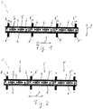
- FIG. 2 of the drawings a schematic top view of an LED light emitting strip according to the invention is shown.
- This claim differs from the claim of fig. 1 in that a plurality of pairs of contact stripes 5', 6'; 5", 6" are provided in a row along the length direction. Each pair of contact stripes thereby corresponds to an individual segment 9, 9', 9" of the LED light emitting strip.
- Each segment 9, 9', 9" comprises a group of LED chips 4 contacted to the contact stripes 5, 6; 5', 6'; 5", 6" of the corresponding pair.
- the respective pairs of contact stripes are isolated or distanced from each other and configured to supply the LED chips 4 of the respective group.
- Each pair of contact stripes 5, 6; 5', 6'; 5", 6" is configured individually controllable to individually light the LED Chips of the corresponding segment 9, 9', 9" of the light emitting strip 1. This is realized in that the terminals corresponding to each pair of contact stripes are connected to an external control unit (not shown), which is configured to individually provide a suitable supply voltage and current for each terminal.
- the LED light emitting strip and the control unit may be comprised in an independent lighting.
- a control unit may be implemented in a control system of a vehicle.
- the lighting system comprises the LED light emitting strip and is configured to be connected to a control system of a vehicle.
- Such a lighting system may comprise an arrangement of at least two LED light emitting strips.
- FIG. 3 of the drawings a schematic top view of an arrangement 100 of LED light emitting strips 1, 1' is shown.
- the first and second LED light emitting strips 1, 1' are configured according to fig. 1 . They are shown in a section, which is near a connection region where the first and second LED light emitting strips 1 and 1' are mated or joined. Furthermore, for a better overview only, the contacts of the LED chips 4 are hidden in fig 3 .
- connection between the mated or joined light emitting strips 1, 1' can be realized in various ways.
- the connection may be realized for example by means of a bracket, a connector, or by means of firmly bonding the light emitting strips, for example by soldering, welding or adhesive bonding.
- At least one of the contact stripes 5, 6 may be configured to connect the light emitting strips, which will be explained in more detail with respect to figs. 4 and 5 .
- a gap between the first and second LED light emitting strips 1, 1' may be free in the air (filled with air) or filled with any light transmitting material, such as glass, a transparent polymer, transparent epoxy resin or transparent ceramic.
- the LED chips 4 are arranged in a regular row with a predetermined distance between them, which is a first distance x1.
- the first and second light emitting strips are mated or joined with each other in a butt configuration, wherein a second distance x2 is provided between a last LED chip 4' of the row of the first light emitting strip 1 and a first LED chip 4" of the row of the second light emitting strip 1'.
- the second distance is adapted to the first distance.
- the LED light emitting strips 1, 1' are connected to each other with a connection invisible from outside, when the LED light emitting strips are lighted.
- the first length x1 is equal to the second length x2.
- a length of the second distance x2 thus is preferably at least 90 % of a length of the first distance x1 and the second distance x2 is equal to or less than the sum x3 of the first distance x1 and the length of one LED chip 4. This results in a deviation or difference between the first and second distances, which is hardly recognizable from outside.
- FIG. 4 of the drawings a schematic top view of an arrangement of LED light emitting strips 1, 1' according to another comparative example is shown.
- an end 10 of the contact stripes 5, 6 is formed female or socket shaped. This is realized, in that the end 10 of the contact stripes 5, 6 respectively extends over the corresponding end of the substrate 2 of the light emitting strip 1. In this way, the end 10 of the contact stripes 5, 6 is configured to accommodate an end 12 of the substrate 2 of the second light emitting strip 1' extending from an end 11 of the second light emitting strip 1'.
- the end 10 of the contact stripes 5, 6 is formed to enclose the end 12 of the substrate 2 of the second light emitting strip 1'.
- the light emitting strips 1, 1' thus can be connected to each other by inserting the end 12 of the substrate 2 of the second light emitting strip 1' into the female or socket shaped end 10.
- FIG. 5 of the drawings a schematic top view of an arrangement of LED light emitting strips according to yet another comparative example is shown.
- an end 10 of the contact stripes 5, 6 is also formed female or socket shaped.
- the end 10 of the contact stripes 5, 6 respectively is widened in the transverse direction 7.
- the end 10 of the contact stripes 5, thus extends over the corresponding end of the substrate 2 of the light emitting strip 1 in a widened manner.
- the end 10 of the contact stripes 5, 6 is configured to accommodate the complete end 11 of the second light emitting strip 1' including the ends 13 and 14 of the contact stripes 5, 6 thereof.
- the ends 13 and 14 thus can be directly connected mechanically and electrically to the contact stripes 5, 6 of the first light emitting strip 1.
- the light emitting strips 1, 1' thus can be connected mechanically and electrically to each other by inserting the ends 13, 14 of the contact stripes 5, 6 of the second light emitting strip 1' into the female or socket shaped end 10.
Landscapes
- Engineering & Computer Science (AREA)
- General Engineering & Computer Science (AREA)
- Microelectronics & Electronic Packaging (AREA)
- Physics & Mathematics (AREA)
- Optics & Photonics (AREA)
- Manufacturing & Machinery (AREA)
- Metallurgy (AREA)
- Led Device Packages (AREA)
- Fastening Of Light Sources Or Lamp Holders (AREA)
- Non-Portable Lighting Devices Or Systems Thereof (AREA)
Description
- The present invention relates to a LED light emitting strip and to an arrangement of LED light emitting strips. The present invention also relates to a method of manufacturing such an arrangement of LED light emitting strips and to an automotive lighting system that includes such a LED light emitting strip or arrangement of LED light emitting strips.
- An LED (light emitting diode) light emitting trip usually comprises a row of LED chips, which are usually embedded in a transparent encapsulant and contacted in series from one end of the LED strip to the other. Such an LED strip is described for example in
US 2013/0058080 A1 . Other prior art LED strips are disclosed byUS 2008/101070 A1 ,DE 20 2014 001943 U1 andUS 2014/062316 A1 . - In lighting systems, especially in automotive lighting systems, comprising one or more LED light emitting strips, a number of LED strips is usually arranged next to each other but not connected. Transitions between the strips are usually avoided, because a connection between such LED light emitting strips is visible as a dark area when the LEDs are lighted. Therefore, a conventional approach for automotive LED light emitting strips comprises a light guiding element formed as a strip, in which light of an LED is distributed. Such a strip is described in
US 2013/0229815 A1 . This kind of LED lighted strips, however, is limited in design. On one hand, there is a limitation regarding a necessary minimum diameter of the light guiding element, which is needed to couple a desired amount of light into the light guiding element. On the other hand, a minimum bending radius or curvature of the light guiding element is limited since guiding properties in such light guiding elements are based on the principle of total reflection. The necessary minimum bending radius or curvature is needed to totally reflect the light in the light guiding element, which otherwise would be coupled out. - In view of the above, an object of the present invention is to provide a new and improved LED light emitting strip for an automotive lighting system, and an arrangement of such LED light emitting strips. The present invention also relates to a method of manufacturing such an arrangement of LED light emitting strips and to an automotive lighting system that includes such a LED light emitting strip or arrangement of LED light emitting strips.
- In accordance with the present invention, an LED light emitting strip as recited in
claim 1, an arrangement of LED light emitting strips as recited in claim : 9 or as recited in claim : 11, a method of manufacturing an arrangement of LED light emitting strips as recited inclaim 13 and an automotive lighting system as recited in claim : 15 are provided. Advantageous or preferred features of the invention are recited in the dependent claims. - According to one aspect, therefore, the present invention provides a LED light emitting strip for an automotive lighting system, comprising: a substrate extending along a length direction of the strip; a plurality of LED chips arranged on or in the substrate, wherein the LED chips are arranged in at least one row along the length direction; at least two contact stripes configured to supply the LED chips with electric energy, wherein each of the contact stripes individually extends, at least partially, along a side of the substrate in the length direction, and wherein the LED chips are contacted to the contact stripes at least partially in a transverse or oblique direction of the strip, wherein a plurality of pairs of contact stripes are provided in a row along the length direction such that each pair of contact stripes corresponds to an individual segment of the light emitting strip, and wherein each pair of contact stripes is configured individually controllable to individually actuate or light the corresponding segment of the light emitting strip.
- In this way, the invention provides an LED light emitting strip which is configured for providing connections or transitions between LED light emitting strips, which are invisible from outside when the LED light emitting strips are lighted, in particular without any need for a light guiding element.
- This is realized in that the contact stripes, which are isolated from each other and individually extend along a side (longitudinal side) of the substrate in length direction, allow a free configuration of a distance between a last LED chip in the row on or in the substrate and an end of the LED light emitting strip. In particular, according to the invention, there is no need for a contact at an end face of the substrate. In this way, the distance between the last LED of a first end of a LED light emitting strip and a first LED of a second end of a LED light emitting strip, which first and second ends are to be connected, can be adapted to the distance between two LED chips in a row of the LED light emitting strip.
- The first and second ends, which are to be connected, may belong to different LED light emitting strips, e. g. connected to each other in a butt configuration. However, the first and second ends may also belong to the same LED light emitting strip, which in this case is circuitously formed or comprises an otherwise formed closed shape.
- The LED light emitting strip of the invention allows new ways of lighting design, in particular in the field of automotive lighting, since an LED light emitting strip of the invention is much smaller in its diameter compared to conventional automotive light emitting strips including light guiding elements. In particular, contact stripes can be designed very thin. Thus, the size of a minimum diameter of a light emitting strip according to the invention even may be in the scale of the size of the LED chips.
- Furthermore, The LED light emitting strip of the invention allows any desired bending radius or curvature. Additionally, since there is neither any need for a light guiding element nor any need to contact the LED chips in series, there is no limitation for the length of an LED light emitting strip according to the invention, even with a completely straight forms of the strip. In contrast, according to the present invention, any length of a LED light emitting strip can be realized, in particular with a similar density of LED chips and light emission.
- Furthermore, according to the present invention, closed geometries of a LED light emitting strip can be easily realized just by connecting the two ends of the light emitting strip, in particular without any need for further measures.
- The substrate preferably forms a structural basis of the LED light emitting strip. In particular for automotive applications, the substrate does not necessarily have to be transparent. It may be even desirable for automotive applications to direct the light emitted from the LED chips at a defined radiation angle smaller than 180°.
- The LED chips on or in the substrate are preferably fixed to the substrate or embedded therein. The at least one row of LED chips along the length direction preferably is configured as a regular row, in particular with equal distances between the LED chips.
- The contact stripes may be connected or fixed to the substrate or integrally formed therewith. In particular, the contact stripes may be arranged on opposite sides of the substrate.
- The contacts of the LED chips may be formed, for example, as wirebonds or conductor paths. They can be fixed to the LED chips and contact strips and/or fixed to or embedded in the substrate. The position of the contacts can be advantageously adapted to any special requirements, since the contact stripes provide for various arrangements of the contacts.
- In a preferred claim a surface of the substrate is configured with a high reflectance. In this way, the substrate functions as a reflector to direct light emitted from the LEDs to a desired direction. Therefore, the LED light emitting strip according to the invention is particularly suitable for automotive lighting systems.
- In another preferred claim, the substrate is configured plastically deformable. In this way, the LED light emitting strip can be freely formed or shaped in the manufacturing process in a very flexible way and afterwards keeps the form or shape. The LED light emitting strip thus can be used for various different applications, in particular in the interior and/or exterior of a vehicle. In particular, a plastically deformable material of the substrate has a ductility sufficient for forming the LED light emitting strip in the manufacturing process of a lighting system in a desired way, without any cracks or damage of the substrate.
- According to a preferred claim, the substrate comprises a metal. Therefore, on one hand, the material of the substrate can be selected to be plastically deformable in a desired way. On the other hand, the material of the substrate thus can be selected to have a high thermal conductivity for improved thermal management and/or an equal temperature distribution along the length direction of the LED light emitting strip.
- According to another preferred claim, the substrate is formed integral with at least one of the contact stripes. Accordingly, the substrate may be configured as one of the at least two contact stripes. Furthermore, the substrate may connect multiple terminals or multiple contact stripes of the same polarity. In this case, an isolation is provided between the substrate and any contact stripe of opposite polarity. With such an integral design, the number of parts can be advantageously reduced. Reduction of parts, in turn, facilitates the manufacturing of the LED light emitting strip.
- According to another preferred claim, the at least two contact stripes each comprise a plurality of terminals for additionally applying supply voltage to the LED chips. In particular, each contact stripe comprises at least two terminals. The terminals are distributed along the contact stripe and apply supply voltage at different parts or sections thereof. In this way, a decrease of voltage over the length of the contact stripe, which otherwise, in particular in very long LED light emitting strings, can arise through resistance heating, is avoided. Furthermore functional reliability is improved, since the terminals form redundant supplies for the contact stripes.
- According to another preferred claim, a first terminal of a respective contact stripe is arranged at a section of the contact stripe distinct from the section of a second terminal. In this way, different sections of the contact stripe are each directly supplied with voltage. The section of the first terminal may be connected to the section of the second terminal via the respective contact stripe. Alternatively, the sections may be isolated from each other.
- According to another preferred claim, the at least one of the contact stripes is configured for mating or joining the light emitting strip with another light emitting strip. In this way, the contact stripe additionally serves as a mechanical connecting element for connecting two light emitting strips. The contact stripe therefore combines multiple functions of supplying the LED chips of a LED light emitting strip with electric energy and of mechanically connecting the LED light emitting strips in one part or element. In case of an integrated design of the contact stripe with a substrate, preferably a reflective and/or metallic substrate as described above, even more functions may be combined in this one part or element.
- According to another preferred claim, an end of at least one of the contact stripes is formed female or socket shaped. The end of the at least one of the contact stripes is configured to accommodate an end of the other light emitting strip.
- Alternatively or in addition, the end of the at least one of the contact stripes is configured to accommodate an end of at least one of the contact stripes of the other light emitting strip. The female or socket shaped end may thereby be formed with the contact stripes and the substrate.
- In particular, the female or socket shaped end of the at least one of the contact stripes extends over the corresponding end of the light emitting strip, in particular at least over the corresponding end of the substrate. In this way, the light emitting strips can be easily connected to each other by sticking, plugging or inserting the end of the other light emitting strip, in particular an end of the substrate thereof, into the female or socket shaped end. Alternatively or in addition, the light emitting strips can be easily connected to each other by sticking, plugging or inserting the end of at least one of the contact stripes of the other light emitting strip into the female or socket shaped end.
- According to another preferred claim, the LED chips of at least one segment of the light emitting strip are contacted with the contact strips in parallel to LED chips of at least one other segment of the light emitting strip. In this way, the segments can be supplied with current/voltage individually and the functional reliability and safety is improved.
- According to the invention, a plurality of pairs of contact stripes are provided in a row along the length direction such that each pair of contact stripes corresponds to an individual segment of the LED light emitting strip. In this way, each segment of the LED light emitting strip is supplied individually by a pair of contact stripes.
- According to another preferred claim, the respective pairs of contact stripes are isolated or distanced from each other and each pair of contact stripes is configured to supply LED chips of the corresponding segment of the light emitting strip. In this way, each segment of the LED light emitting strip can be independently supplied with electric energy and therefore lighted independent from the other segments.
- According to the invention, each pair of contact stripes is configured individually controllable to individually light the corresponding segment of the light emitting strip. In particular, the segments are configured to be controlled by an external control unit such that they can be individually lighted. Accordingly, the segments of the LED light emitting strip can be specifically lighted in a desired pattern or sequence.
- According to another preferred claim, the LED chips arranged in the at least one row are positioned apart from each other with a predetermined distance. In this way, a regular outer appearance of the LED string is provided.
- According to a further aspect, the present invention provides an arrangement of light emitting strips, comprising: a first light emitting strip and a second light emitting strip, wherein at least one of the first and second light emitting strips is configured as light emitting strip according to the invention, and wherein the first and second light emitting strips are mated or joined with each other.
- As discussed above, the invention is configured for providing connections between LED light emitting strips, which are invisible from outside when the LED light emitting strips are lighted. In this way, connections between the two or more LED light emitting strips in an arrangement of such strips are invisible from outside when the LED light emitting strips are lighted.
- Two or more LED light emitting strips may be arranged and connected in a butt-configuration or arranged and connected in another possible configuration, for example a configuration in T-form, L-form, V-form, Y-form, X-form, star form, Z-form or the like.
- In a preferred claim, an end of the first light emitting strip is mated or joined with an end of the second light emitting strip. The first and second light emitting strips may be arranged in a butt-configuration or oriented at any angle to each other.
- According to a further aspect, the present invention provides an arrangement of light emitting strips, comprising: a first light emitting strip and a second light emitting strip, wherein at least one of the first and second light emitting strips is configured as light emitting strip according to the invention, wherein the LED chips arranged in the at least one row are positioned apart from each other with a predetermined distance, wherein the predetermined distance between the LED chips arranged in the at least one row is a first distance, wherein the first and second light emitting strips are mated or joined with each other, wherein a second distance between a last LED chip of a row of the first light emitting strip and a first LED chip of a row of the second light emitting strip is provided adapted to the first distance.
- As discussed above, the invention is configured for providing connections between LED light emitting strips, which are invisible from outside when the LED light emitting strips are lighted. The length of the second distance can be adapted in that the contact stripes individually extending along a side of the substrate in the length direction allow a free configuration of a distance between a last LED and an end of the LED light emitting strip. In particular, there is no need for a contact at an end face of the substrate. In contrast, a transition between the ends of the LED light emitting strips provides a second distance, which has no or only small deviation from the first distance. The LED light emitting strips thus may be connected to each other, e. g. in a butt configuration, with a connection between the LED light emitting strips invisible or only hardly visible from outside when the LED light emitting strips are lighted.
- In a preferred claim, a length of the second distance is at least 90 % of a length of the first distance.
- According to another preferred claim, the LED chips have a uniform length, and the second distance is equal to or less than the sum of the first distance and the length of one LED chip. In this way, a difference between the first and second distances is hardly recognizable from outside.
- According to another aspect, the invention provides a method of manufacturing an arrangement of light emitting strips according to the invention, comprising the steps of: positioning a first light emitting strip relative to a second light emitting strip, wherein at least the first light emitting strip comprises at least two contact stripes, wherein each of the contact stripes, at least partially, extends along a side of a substrate of the first light emitting strip in a length direction of the first light emitting strip, wherein at least one of the contact stripes is configured for mating or joining the first light emitting strip with the second light emitting strip; and mating or joining the first and second light emitting strips by means of the at least one of the contact stripes.
- As discussed above, the invention is configured for providing connections between LED light emitting strips, which are invisible from outside when the LED light emitting strips are lighted. In this way, an arrangement of two or more LED light emitting strips can be manufactured such that connections between the two or more LED light emitting strips are invisible from outside when the LED light emitting strips are lighted. Therefore, the first and second light emitting strips are mated or joined by means of or with or by use of the at least one of the contact stripes
- Two or more LED light emitting strips may be arranged and mated or joined in any configuration of an arrangement, for example a configuration in T-form, L-form, V-form, Y-form, X-form, star form, Z-form or the like, wherein the mated or joined connections between individual light emitting strips are invisible from outside when the LED light emitting strips are lighted.
- In a preferred claim, an end of the at least one of the contact stripes is formed female or socket shaped and is configured to accommodate an end of the second light emitting strip, wherein the step of mating or joining the first and second light emitting strips by means of the least one of the contact stripes comprises inserting the end of the second light emitting strip into the female or socket shaped end. In this way, the light emitting strips can be easily connected without a need for firmly bonding. However, alternatively or in addition, the ends of the light emitting strips may be firmly bonded, for example by soldiering, welding or adhesive bonding.
- According to a preferred claim, the female or socket shaped end is configured to accommodate an end of at least one contact stripe of the second light emitting strip, wherein inserting the end of the second light emitting strip into the female or socket shaped end comprises inserting the end of the at least one contact stripe of the second light emitting strip into the female or socket shaped end. In this way, the contact stripes of the first light emitting strip are directly contacted to the contact stripes of the second light emitting strip.
- According to another preferred claim, the female or socket shaped end is configured to accommodate an end of a substrate of the second light emitting strip, wherein inserting the end of the second light emitting strip into the female or socket shaped end comprises inserting the end of the substrate of the second light emitting strip into the female or socket shaped end. In this way, a connection between the contact stripes of the first light emitting strip and the substrate of the second light emitting strip is provided. A connection of the contact stripes of the first and the second light emitting strips can therefore be avoided.
- According to a further aspect, the present invention provides an automotive lighting system which comprises a light emitting strip according to the invention or an arrangement of light emitting strips according to the invention or an arrangement of light emitting strips manufactured according to a method according to the invention.
- The automotive lighting system may be configured for interior or exterior or interior and exterior vehicle lighting. An interior lighting system may e.g. be configured for ambient lighting. An exterior lighting system may comprise or be configured as an indicator, brake light, daytime running light or the like.
- A control unit may be comprised in an independent lighting system to control the light emitting strips. Alternatively or in addition, a control unit may be implemented in a control system of a vehicle. In this case, the lighting system is configured to be connected to a control system of a vehicle.
- The light emitting strip may be a so-called Chip-on-Board light emitting strip. A Chip-on-Board light emitting strip - or shortly COB light emitting strip - is manufactured by employing methods of directly mounting integrated circuits on substrates. This means that the single LED chips or LED die are mounted onto the substrate without using SMD technologies und preferably also without using printed boards, printed circuit boards (PCB) and the like. This means that the LED chips are not soldered onto a PCB. Generally, the chip-on-board technology is a process for the direct mounting of unpackaged semiconductor chips on suitable substrates to an electronic assembly. In the context of the present invention the term "chip" is to be understood as a non-packaged semiconductor device. An LED-chip is consequently one single LED die.
- For a more complete understanding of the invention and the advantages thereof, exemplary claims of the invention are explained in more detail in the following description with reference to the accompanying drawing figures, in which like reference characters designate like parts and in which:
- Fig. 1
- is a schematic top view of an LED light emitting strip of a comparative example not forming part of the invention;
- Fig. 2
- is a schematic top view of an LED light emitting strip according to the invention;
- Fig. 3
- is a schematic top view of an arrangement of LED light emitting strips of a comparative example not forming part of the invention;
- Fig. 4
- is a schematic top view of an arrangement of LED light emitting strips according to another comparative example not forming part of the invention;
- Fig. 5
- is a schematic top view of an arrangement of LED light emitting strips according to yet another comparative example not forming part of the invention.
- The accompanying drawings are included to provide a further understanding of the present invention and are incorporated in and constitute a part of this specification. The drawings illustrate particular claims of the invention and together with the description serve to explain the principles of the invention. Other claims of the invention and many of the attendant advantages of the invention will be readily appreciated as they become better understood with reference to the following detailed description.
- It will be appreciated that common and/or well understood elements that may be useful or necessary in a commercially feasible claim are not necessarily depicted in order to facilitate a more abstracted view of the claims. The elements of the drawings are not necessarily illustrated to scale relative to each other. It will further be appreciated that certain actions and/or steps in an claim of a method may be described or depicted in a particular order of occurrences while those skilled in the art will understand that such specificity with respect to sequence is not actually required. It will also be understood that the terms and expressions used in the present specification have the ordinary meaning as is accorded to such terms and expressions with respect to their corresponding respective areas of inquiry and study, except where specific meanings have otherwise been set forth herein.
- With reference firstly to
Fig. 1 of the drawings, a top view of an LEDlight emitting strip 1 according to a comparative example not forming part of the invention is illustrated schematically. In particular, a section of an LEDlight emitting strip 1 is shown. Therefore, the length of the LEDlight emitting strip 1 is not limited to the length as shown, but may have any desired extend. - The
light emitting strip 1 includes asubstrate 2, a plurality ofLED chips 4 arranged on thesubstrate 2, afirst contact stripe 5 and asecond contact stripe 6. - The
substrate 2 extends along a length direction 3 of the LEDlight emitting strip 1. In the claim shown infig. 1 , the LED light emitting strip is a thin and long strip formed straight. However, the disclosure is not limited to such a straight configuration. A thin and long LED light emitting strip may also be formed bended or curved. In this case, the length direction changes as a function of the length of the strip. - The
contact stripes LED chips 4 arranged on thesubstrate 2 with electric energy in order to light theLED chips 4. Therefore, thecontact stripes - The
contact stripes light emitting strip 1, each along a side of thesubstrate 2. For example only, thecontact stripes - In the example shown, the substrate is formed of a transparent material, in particular the transparent polymer or resin.
- Alternatively, the substrate may be formed integrally with one of the
contact stripes substrate 2, it comprises a conductive metal, which preferably is configured plastically deformable. In this case, the metal surface of the substrate preferably is also configured with a high reflectance. - The LED chips 4 are arranged on the
substrate 2 in a regular row along the length direction 3. In such a regular row, distances between the LED chips are preferably equal. - In order to supply the
LED chips 4 with electric energy, theLED chips 4 are contacted to thecontact stripes LED chip 4 to one of thecontact stripes - In other LED strips, however, the LED chips may also be contacted to the
contact stripes LED chip 4 to one of thecontact stripes - In the exemplary LED strip of
fig. 1 , theLED chips light emitting strip 1 comprises nine LED chips arranged in a row, connected in three groups along the LEDlight emitting strip 1. - Each group comprises a
first LED chip 4 connected to thefirst contact stripe 5 in the transverse direction 7, a second LED chip 4' arranged in the middle and contacted to thefirst LED chip 4 in length direction 3, and athird LED chip 4" connected to the second LED chip 4' in length direction 3 and connected to thesecond contact stripe 6 in the transverse direction 7. - Each group is arranged on a part of the LED
light emitting strip 1. The LED chips 4, 4', 4" of such a part or group are contacted with a section of thecontact stripes LED chips contact stripes contact stripes - In the exemplary LED strip of
fig. 1 , thecontact stripes substrate 2. Furthermore, thecontact stripes terminals 8 for additionally applying supply voltage to theLED chips 4. Afirst terminal 8 of arespective contact stripe contact stripes contact stripes - As an example only, each of the
contact stripes terminals terminals respective contact stripe contact stripes contact stripes - Additionally, the LED chips may be encapsulated in a transparent or partly transparent encapsulating layer, for example of silicone, epoxy resin or polymer. In case of a
transparent substrate 2, the encapsulating layer may be formed integrally with thesubstrate 2 and protect the LED chips from humidity and mechanical impact. In this case, thesubstrate 2 and the contacts may be, at least in part, encapsulated or embedded in the encapsulant, too. - A lighting material, such as e. g. a fluorescent material, may be comprised in the encapsulating layer. Alternatively or in addition, a lighting material may be deposited on the transparent layer or directly on the LED chips.
- In the exemplary LED strip of
fig. 1 , thecontact stripes contact stripes substrate 2 in length direction 3. - With reference now also to
Fig. 2 of the drawings, a schematic top view of an LED light emitting strip according to the invention is shown. - This claim differs from the claim of
fig. 1 in that a plurality of pairs of contact stripes 5', 6'; 5", 6" are provided in a row along the length direction. Each pair of contact stripes thereby corresponds to an individual segment 9, 9', 9" of the LED light emitting strip. - Each segment 9, 9', 9" comprises a group of
LED chips 4 contacted to thecontact stripes LED chips 4 of the respective group. Each pair ofcontact stripes light emitting strip 1. This is realized in that the terminals corresponding to each pair of contact stripes are connected to an external control unit (not shown), which is configured to individually provide a suitable supply voltage and current for each terminal. - The LED light emitting strip and the control unit may be comprised in an independent lighting. Alternatively or in addition, a control unit may be implemented in a control system of a vehicle. In this case, the lighting system comprises the LED light emitting strip and is configured to be connected to a control system of a vehicle.
- Such a lighting system may comprise an arrangement of at least two LED light emitting strips.
- With reference now also to
Fig. 3 of the drawings, a schematic top view of anarrangement 100 of LEDlight emitting strips 1, 1' is shown. - As an example only, the first and second LED
light emitting strips 1, 1' are configured according tofig. 1 . They are shown in a section, which is near a connection region where the first and second LEDlight emitting strips 1 and 1' are mated or joined. Furthermore, for a better overview only, the contacts of theLED chips 4 are hidden infig 3 . - An end of the first
light emitting strip 1 is mated or joined with an end of the second light emitting strip 1'. The connection between the mated or joined light emittingstrips 1, 1' can be realized in various ways. The connection may be realized for example by means of a bracket, a connector, or by means of firmly bonding the light emitting strips, for example by soldering, welding or adhesive bonding. - In particular, at least one of the
contact stripes figs. 4 and 5 . - A gap between the first and second LED
light emitting strips 1, 1' may be free in the air (filled with air) or filled with any light transmitting material, such as glass, a transparent polymer, transparent epoxy resin or transparent ceramic. - The LED chips 4 are arranged in a regular row with a predetermined distance between them, which is a first distance x1. The first and second light emitting strips are mated or joined with each other in a butt configuration, wherein a second distance x2 is provided between a last LED chip 4' of the row of the first
light emitting strip 1 and afirst LED chip 4" of the row of the second light emitting strip 1'. - The second distance is adapted to the first distance. Thus, the LED
light emitting strips 1, 1' are connected to each other with a connection invisible from outside, when the LED light emitting strips are lighted. - In the exemplary arrangement shown, the first length x1 is equal to the second length x2. In other arrangements, deviations are possible. A length of the second distance x2 thus is preferably at least 90 % of a length of the first distance x1 and the second distance x2 is equal to or less than the sum x3 of the first distance x1 and the length of one
LED chip 4. This results in a deviation or difference between the first and second distances, which is hardly recognizable from outside. - With reference now also to
Fig. 4 of the drawings, a schematic top view of an arrangement of LEDlight emitting strips 1, 1' according to another comparative example is shown. - According to this example, an end 10 of the
contact stripes contact stripes substrate 2 of thelight emitting strip 1. In this way, the end 10 of thecontact stripes substrate 2 of the second light emitting strip 1' extending from anend 11 of the second light emitting strip 1'. - The end 10 of the
contact stripes substrate 2 of the second light emitting strip 1'. Thelight emitting strips 1, 1' thus can be connected to each other by inserting the end 12 of thesubstrate 2 of the second light emitting strip 1' into the female or socket shaped end 10. - Finally, referring to
Fig. 5 of the drawings, a schematic top view of an arrangement of LED light emitting strips according to yet another comparative example is shown. - According to this example, an end 10 of the
contact stripes Fig. 4 , this is realized, in that the end 10 of thecontact stripes contact stripes 5, thus extends over the corresponding end of thesubstrate 2 of thelight emitting strip 1 in a widened manner. In this way, the end 10 of thecontact stripes complete end 11 of the second light emitting strip 1' including theends contact stripes contact stripes light emitting strip 1. - The
light emitting strips 1, 1' thus can be connected mechanically and electrically to each other by inserting theends contact stripes - Although specific embodiments of the invention are illustrated and described herein, it will be appreciated by those of ordinary skill in the art that a variety of alternate and/or equivalent implementations exist. It should be appreciated that the exemplary embodiments are examples only and are not intended to limit the scope, applicability, or configuration in any way. Rather, the foregoing summary and detailed description will provide those skilled in the art with a convenient road map for implementing at least one embodiment, it being understood that various changes may be made in the function and arrangement of elements described in an exemplary claim without departing from the scope as set forth in the appended claims.
- It will also be appreciated that in this document the terms "comprise", "comprising", "include", "including", "contain", "containing", "have", "having", and any variations thereof, are intended to be understood in an inclusive (i.e. non-exclusive) sense, such that the process, method, device, apparatus or system described herein is not limited to those features or parts or elements or steps recited but may include other elements, features, parts or steps not expressly listed or inherent to such process, method, article, or apparatus. Furthermore, the terms "a" and "an" used herein are intended to be understood as meaning one or more unless explicitly stated otherwise. Moreover, the terms "first", "second", "third", etc. are used merely as labels, and are not intended to impose numerical requirements on or to establish a certain ranking of importance of their objects.
Claims (15)
- LED light emitting strip (1) for an automotive lighting system, comprising:a substrate (2) extending along a length direction (3) of the strip;a plurality of LED chips (4) arranged on or in the substrate (2), wherein the LED chips (4) are arranged in at least one row along the length direction (3);at least two contact stripes (5, 6) configured to supply the LED chips (4) with electric energy,wherein each of the contact stripes (5, 6) individually extends, at least partially, along a side of the substrate (2) in the length direction (3),wherein the LED chips (4) are contacted to the contact stripes (5, 6) at least partially in a transverse or oblique direction (7) of the strip (1),wherein a plurality of pairs of contact stripes (5, 6, 5', 6', 5", 6") are provided in a row along the length direction (3) such that each pair of contact stripes (5, 6, 5', 6', 5", 6") corresponds to an individual segment (9, 9', 9") of the light emitting strip, andcharacterised in that each pair of contact stripes (5, 6; 5', 6'; 5", 6") is configured to be individually controllable to individually light the corresponding segment (9; 9'; 9") of the light emitting strip (1).
- Light emitting strip according to claim 1, wherein a surface of the substrate (2) is configured with a high reflectance and/or wherein the substrate (2) is configured plastically deformable.
- Light emitting strip according to any one of the preceding claims, wherein the substrate (2) comprises a metal, in particular wherein the substrate (2) is formed integral with at least one of the contact stripes (5; 6) .
- Light emitting strip according to any one of the preceding claims, wherein the at least two contact stripes (5, 6) each comprise a plurality of, in particular at least two, terminals (8) for additionally applying supply voltage to the LED chips (4), in particular wherein a first terminal (8') of a respective contact stripe (5) is arranged at a section of the contact stripe (5) distinct from the section of a second terminal (8").
- Light emitting strip according to any one of the preceding claims, wherein at least one of the contact stripes (5, 6) is configured for mating or joining the light emitting strip (1) with another light emitting strip (1'), in particular wherein an end (10) of at least one of the contact stripes (5, 6) is formed female or socket shaped and is configured to accommodate an end (11) of the other light emitting strip (1') or to accommodate an end (13; 14) of at least one of the contact stripes (5, 6) of the other light emitting strip (1') or to accommodate an end (12) of the substrate (2) of the of the other light emitting strip (1').
- Light emitting strip according to any one of the preceding claims, wherein the LED chips (4) of at least one part of the light emitting strip (1) are contacted with the contact stripes (5, 6; 5', 6'; 5", 6") in parallel to LED chips (4) of at least one other part of the light emitting strip (1).
- Light emitting strip according to any one of the preceding claims, wherein the respective pairs of contact stripes (5, 6, 5', 6', 5", 6") are isolated or distanced from each other and each pair of contact stripes (5, 6; 5', 6'; 5", 6") is configured to supply LED chips (4) of the corresponding segment (9; 9'; 9") of the light emitting strip (1).
- Light emitting strip according to any one of the preceding claims, wherein the LED chips (4) arranged in the at least one row are positioned apart from each other with a predetermined distance (x1).
- An arrangement (100) of light emitting strips (1, 1') for an automotive lighting system, comprising:
a first light emitting strip (1) and a second light emitting strip (1'), wherein at least one of the first and second light emitting strips (1; 1') is configured as light emitting strip according to one of claims 1 to 8, and
wherein the first and second light emitting strips (1; 1') are mated or joined with each other. - The arrangement according to claim 9, wherein an end (10) of the first light emitting strip (1) is mated or joined with an end (11) of the second light emitting strip (1').
- An arrangement (100) of light emitting strips (1; 1') for an automotive lighting system, comprising:
a first light emitting strip (1) and a second light emitting strip (1'), wherein at least one of the first and second light emitting strips (1; 1') is a light emitting strip according to claim 8,
wherein the predetermined distance (x1) between the LED chips (4) arranged in the at least one row is a first distance,
wherein the first and second light emitting strips (1; 1') are mated or joined with each other, and
wherein a second distance (x2) between a last LED chip (4') of a row of the first light emitting strip (1) and a first LED chip (4") of a row of the second light emitting strip (1') is provided adapted to the first distance. - The arrangement according to claim 11, wherein a length of the second distance (x2) is at least 90 % of a length of the first distance (x1) and/or wherein the second distance (x2) is equal to or less than the sum (x3) of the length of the first distance (x1) and the length of one LED chip (4).
- Method of manufacturing an arrangement of light emitting strips for an automotive lighting system according to any one of claims 9 to 12, comprising the steps of:positioning a first light emitting strip (1) relative to a second light emitting strip (1'), wherein at least the first light emitting strip (1) comprises at least two contact stripes (5, 6), wherein a plurality of pairs of contact stripes (5, 6, 5', 6', 5", 6") are provided in a row along the length direction (3) such that each pair of contact stripes (5, 6, 5', 6', 5", 6") corresponds to an individual segment (9, 9' , 9") of the light emitting strip, wherein each pair of contact stripes (5, 6; 5', 6'; 5", 6") is configured individually controllable to individually actuate or light the corresponding segment (9; 9'; 9") of the light emitting strip (1);wherein each of the contact stripes (5, 6), at least partially, extends along a side of a substrate (2) of the first light emitting strip in a length direction (3) of the first light emitting strip (1), wherein at least one of the contact stripes (5, 6) is configured for mating or joining the first light emitting strip (1) with the second light emitting strip (1'); andmating or joining the first and second light emitting strips (1; 1') by means of the at least one of the contact stripes (5, 6) .
- Method according to claim 13, wherein an end (10) of the at least one of the contact stripes (5, 6) is formed female or socket shaped and is configured to accommodate an end (11) of the second light emitting strip (1'), wherein the step of mating or joining the first and second light emitting strips (1; 1') by means of the least one of the contact stripes (5, 6) comprises inserting the end (11) of the second light emitting strip (1') into the female or socket shaped end (10).
- An automotive lighting system which comprises a light emitting strip (1) according to any one of claims 1 to 8 or an arrangement (100) of light emitting strips according to any one of claims 9 to 12 or an arrangement of light emitting strips manufactured according to a method of any one of claims 13 or 14.
Applications Claiming Priority (1)
| Application Number | Priority Date | Filing Date | Title |
|---|---|---|---|
| US14/996,429 US10801705B2 (en) | 2016-01-15 | 2016-01-15 | LED light emitting strip and arrangement of LED light emitting strips |
Publications (2)
| Publication Number | Publication Date |
|---|---|
| EP3193075A1 EP3193075A1 (en) | 2017-07-19 |
| EP3193075B1 true EP3193075B1 (en) | 2020-08-26 |
Family
ID=57482307
Family Applications (1)
| Application Number | Title | Priority Date | Filing Date |
|---|---|---|---|
| EP16202166.1A Active EP3193075B1 (en) | 2016-01-15 | 2016-12-05 | Led light emitting strip and arrangement of led light emitting strips |
Country Status (6)
| Country | Link |
|---|---|
| US (1) | US10801705B2 (en) |
| EP (1) | EP3193075B1 (en) |
| KR (1) | KR20180103928A (en) |
| CN (1) | CN106989310B (en) |
| CA (1) | CA3010745C (en) |
| WO (1) | WO2017121773A1 (en) |
Families Citing this family (8)
| Publication number | Priority date | Publication date | Assignee | Title |
|---|---|---|---|---|
| DE102016108138A1 (en) * | 2016-05-02 | 2017-11-02 | DSD Dr. Steffan Datentechnik Ges.m.b.H. | Collision Target Dummy |
| US10847701B2 (en) | 2018-09-18 | 2020-11-24 | Aura Technologies, Llc | Semi-flexible lighting module |
| KR102659254B1 (en) * | 2018-12-26 | 2024-04-22 | 엘지전자 주식회사 | Lamp using semiconductor light emitting device |
| DE102019219721A1 (en) * | 2019-12-16 | 2021-06-17 | Vosla Gmbh | LED light strips and vehicle light |
| US11359797B1 (en) | 2020-11-20 | 2022-06-14 | Advanced Lighting Concepts, LLC | Chip-on-board LED lighting devices |
| CN115226295B (en) * | 2021-04-16 | 2025-08-15 | 鹏鼎控股(深圳)股份有限公司 | Splicing method of LED lamp panels and LED lamp panel assembly |
| AT525214B1 (en) * | 2021-07-01 | 2023-07-15 | Ktm Ag | Lighting device for a headlight |
| EP4578731A1 (en) * | 2023-12-28 | 2025-07-02 | Marelli Automotive Lighting Italy S.p.A. | Lighting assembly |
Citations (1)
| Publication number | Priority date | Publication date | Assignee | Title |
|---|---|---|---|---|
| US20140062316A1 (en) * | 2012-09-06 | 2014-03-06 | Michael A. Tischler | Wiring boards for array-based electronic devices |
Family Cites Families (13)
| Publication number | Priority date | Publication date | Assignee | Title |
|---|---|---|---|---|
| JP4241658B2 (en) * | 2005-04-14 | 2009-03-18 | シチズン電子株式会社 | Light emitting diode light source unit and light emitting diode light source formed using the same |
| KR20060134375A (en) * | 2005-06-22 | 2006-12-28 | 삼성전자주식회사 | Back light assembly and display device having same |
| TW200802928A (en) | 2006-06-13 | 2008-01-01 | Bright View Electronics Co Ltd | A flexible ribbon illumination device and manufacture method thereof |
| FR2922295B1 (en) * | 2007-10-12 | 2009-12-04 | In Novea | LIGHTING MODULE HAVING MULTIPLE LIGHT EMITTING DIODES AND LIGHTING ASSEMBLY COMPRISING SUCH A MODULE |
| CA2671360C (en) * | 2008-07-08 | 2017-01-10 | Virginia Optoelectronics, Inc. | Modular led lighting systems and flexible or rigid strip lighting devices |
| JP2012004391A (en) * | 2010-06-17 | 2012-01-05 | Toshiba Lighting & Technology Corp | Light-emitting device and luminaire |
| WO2012031533A1 (en) | 2010-09-08 | 2012-03-15 | 浙江锐迪生光电有限公司 | Led lamp bulb and led lighting bar capable of emitting light over 4π |
| DE102011112321B3 (en) | 2011-09-02 | 2012-08-02 | Audi Ag | Lighting device for generating a light strip and motor vehicles |
| TWI598665B (en) * | 2013-03-15 | 2017-09-11 | 隆達電子股份有限公司 | Light-emitting element, long strip light-emitting element and application thereof |
| US9239136B1 (en) * | 2013-08-14 | 2016-01-19 | Elemental LED, Inc. | Connector for light-emitting diode strip |
| CN103712112B (en) * | 2013-12-18 | 2016-02-24 | 京东方科技集团股份有限公司 | A kind of lamp bar and use the method for this lamp bar determination pointolite spacing |
| DE202014001943U1 (en) | 2014-02-28 | 2014-05-08 | Vosla Gmbh | LED strip, lamp |
| CN104654087A (en) * | 2015-02-03 | 2015-05-27 | 广东昭信照明科技有限公司 | LED (Light Emitting Diode) adjustable line lamp |
-
2016
- 2016-01-15 US US14/996,429 patent/US10801705B2/en active Active
- 2016-12-05 EP EP16202166.1A patent/EP3193075B1/en active Active
-
2017
- 2017-01-11 CN CN201710019783.1A patent/CN106989310B/en active Active
- 2017-01-12 KR KR1020187021550A patent/KR20180103928A/en not_active Ceased
- 2017-01-12 WO PCT/EP2017/050515 patent/WO2017121773A1/en not_active Ceased
- 2017-01-12 CA CA3010745A patent/CA3010745C/en active Active
Patent Citations (1)
| Publication number | Priority date | Publication date | Assignee | Title |
|---|---|---|---|---|
| US20140062316A1 (en) * | 2012-09-06 | 2014-03-06 | Michael A. Tischler | Wiring boards for array-based electronic devices |
Also Published As
| Publication number | Publication date |
|---|---|
| CA3010745C (en) | 2023-10-03 |
| CA3010745A1 (en) | 2017-07-20 |
| EP3193075A1 (en) | 2017-07-19 |
| KR20180103928A (en) | 2018-09-19 |
| US20170205057A1 (en) | 2017-07-20 |
| US10801705B2 (en) | 2020-10-13 |
| CN106989310A (en) | 2017-07-28 |
| WO2017121773A1 (en) | 2017-07-20 |
| CN106989310B (en) | 2021-03-05 |
Similar Documents
| Publication | Publication Date | Title |
|---|---|---|
| CA3010745C (en) | Led light emitting strip and arrangement of led light emitting strips | |
| EP3152477B1 (en) | Leds mounted on curved lead frame | |
| CN101150121B (en) | Flex circuits with improved reliability and heat dissipation | |
| EP2854187B1 (en) | LED device, method of manufacturing the same, and light-emitting apparatus | |
| CN109973837B (en) | LED module with stable lead frame | |
| US20080258169A1 (en) | Substrate for mounting light emitting element, light emitting module and lighting apparatus | |
| US8779694B1 (en) | LEDs on flexible substrate arrangement | |
| CN105830544B (en) | LED substrate with electrical connections through bridges | |
| CN101432899A (en) | Semiconductor light emitting element, method for manufacturing same, and semiconductor light emitting device | |
| US20150338081A1 (en) | Led assembly | |
| US10015883B2 (en) | LED package for lamp of vehicle | |
| EP3555520B1 (en) | Arrangement of leds on a leadframe | |
| US11248757B2 (en) | Lighting device comprising connection element with spring section | |
| CN113545171B (en) | Carrier base module for lighting module | |
| EP3582592A1 (en) | Printed citcuit board, card edge connector socket, electronic assembly and automotive lighting device | |
| US12604772B2 (en) | LED electrical contact for 3D LEDs | |
| US20130215627A1 (en) | Electronic unit base and electronic module and electronic device using the same | |
| US11527689B2 (en) | Optoelectronic assembly, method and molded part | |
| CN209026572U (en) | Lamp bar compliant conductive connector and its flexible lamp strip | |
| CN114341545A (en) | Support for light emitting elements and lighting devices | |
| CN110234925B (en) | Lighting module, lighting system, and method for assembling a lighting system | |
| CN223649132U (en) | LED modules and headlights for vehicles | |
| US9989223B1 (en) | LED lighting apparatus with LEDs and wires attached to metal sheet member by adhesive | |
| WO2024155920A1 (en) | Led lighting system, method of manufacturing the same, and led module | |
| US20180156436A1 (en) | Leadframe, luminaire, group of luminaires and method for producing a luminaire |
Legal Events
| Date | Code | Title | Description |
|---|---|---|---|
| PUAI | Public reference made under article 153(3) epc to a published international application that has entered the european phase |
Free format text: ORIGINAL CODE: 0009012 |
|
| STAA | Information on the status of an ep patent application or granted ep patent |
Free format text: STATUS: THE APPLICATION HAS BEEN PUBLISHED |
|
| AK | Designated contracting states |
Kind code of ref document: A1 Designated state(s): AL AT BE BG CH CY CZ DE DK EE ES FI FR GB GR HR HU IE IS IT LI LT LU LV MC MK MT NL NO PL PT RO RS SE SI SK SM TR |
|
| AX | Request for extension of the european patent |
Extension state: BA ME |
|
| STAA | Information on the status of an ep patent application or granted ep patent |
Free format text: STATUS: REQUEST FOR EXAMINATION WAS MADE |
|
| 17P | Request for examination filed |
Effective date: 20180116 |
|
| RBV | Designated contracting states (corrected) |
Designated state(s): AL AT BE BG CH CY CZ DE DK EE ES FI FR GB GR HR HU IE IS IT LI LT LU LV MC MK MT NL NO PL PT RO RS SE SI SK SM TR |
|
| STAA | Information on the status of an ep patent application or granted ep patent |
Free format text: STATUS: EXAMINATION IS IN PROGRESS |
|
| 17Q | First examination report despatched |
Effective date: 20190523 |
|
| RIC1 | Information provided on ipc code assigned before grant |
Ipc: H01L 25/075 20060101ALN20200226BHEP Ipc: F21S 4/20 20160101AFI20200226BHEP |
|
| GRAP | Despatch of communication of intention to grant a patent |
Free format text: ORIGINAL CODE: EPIDOSNIGR1 |
|
| STAA | Information on the status of an ep patent application or granted ep patent |
Free format text: STATUS: GRANT OF PATENT IS INTENDED |
|
| RIC1 | Information provided on ipc code assigned before grant |
Ipc: F21S 4/20 20160101AFI20200304BHEP Ipc: H01L 25/075 20060101ALN20200304BHEP |
|
| RIC1 | Information provided on ipc code assigned before grant |
Ipc: H01L 25/075 20060101ALN20200313BHEP Ipc: F21S 4/20 20160101AFI20200313BHEP |
|
| RIC1 | Information provided on ipc code assigned before grant |
Ipc: H01L 25/075 20060101ALN20200325BHEP Ipc: F21S 4/20 20160101AFI20200325BHEP |
|
| INTG | Intention to grant announced |
Effective date: 20200407 |
|
| GRAS | Grant fee paid |
Free format text: ORIGINAL CODE: EPIDOSNIGR3 |
|
| GRAA | (expected) grant |
Free format text: ORIGINAL CODE: 0009210 |
|
| STAA | Information on the status of an ep patent application or granted ep patent |
Free format text: STATUS: THE PATENT HAS BEEN GRANTED |
|
| AK | Designated contracting states |
Kind code of ref document: B1 Designated state(s): AL AT BE BG CH CY CZ DE DK EE ES FI FR GB GR HR HU IE IS IT LI LT LU LV MC MK MT NL NO PL PT RO RS SE SI SK SM TR |
|
| REG | Reference to a national code |
Ref country code: GB Ref legal event code: FG4D |
|
| REG | Reference to a national code |
Ref country code: CH Ref legal event code: EP |
|
| REG | Reference to a national code |
Ref country code: AT Ref legal event code: REF Ref document number: 1306725 Country of ref document: AT Kind code of ref document: T Effective date: 20200915 |
|
| REG | Reference to a national code |
Ref country code: IE Ref legal event code: FG4D |
|
| REG | Reference to a national code |
Ref country code: DE Ref legal event code: R096 Ref document number: 602016042662 Country of ref document: DE |
|
| REG | Reference to a national code |
Ref country code: SK Ref legal event code: T3 Ref document number: E 35513 Country of ref document: SK |
|
| REG | Reference to a national code |
Ref country code: LT Ref legal event code: MG4D |
|
| PG25 | Lapsed in a contracting state [announced via postgrant information from national office to epo] |
Ref country code: SE Free format text: LAPSE BECAUSE OF FAILURE TO SUBMIT A TRANSLATION OF THE DESCRIPTION OR TO PAY THE FEE WITHIN THE PRESCRIBED TIME-LIMIT Effective date: 20200826 Ref country code: GR Free format text: LAPSE BECAUSE OF FAILURE TO SUBMIT A TRANSLATION OF THE DESCRIPTION OR TO PAY THE FEE WITHIN THE PRESCRIBED TIME-LIMIT Effective date: 20201127 Ref country code: FI Free format text: LAPSE BECAUSE OF FAILURE TO SUBMIT A TRANSLATION OF THE DESCRIPTION OR TO PAY THE FEE WITHIN THE PRESCRIBED TIME-LIMIT Effective date: 20200826 Ref country code: NO Free format text: LAPSE BECAUSE OF FAILURE TO SUBMIT A TRANSLATION OF THE DESCRIPTION OR TO PAY THE FEE WITHIN THE PRESCRIBED TIME-LIMIT Effective date: 20201126 Ref country code: PT Free format text: LAPSE BECAUSE OF FAILURE TO SUBMIT A TRANSLATION OF THE DESCRIPTION OR TO PAY THE FEE WITHIN THE PRESCRIBED TIME-LIMIT Effective date: 20201228 Ref country code: BG Free format text: LAPSE BECAUSE OF FAILURE TO SUBMIT A TRANSLATION OF THE DESCRIPTION OR TO PAY THE FEE WITHIN THE PRESCRIBED TIME-LIMIT Effective date: 20201126 Ref country code: LT Free format text: LAPSE BECAUSE OF FAILURE TO SUBMIT A TRANSLATION OF THE DESCRIPTION OR TO PAY THE FEE WITHIN THE PRESCRIBED TIME-LIMIT Effective date: 20200826 Ref country code: HR Free format text: LAPSE BECAUSE OF FAILURE TO SUBMIT A TRANSLATION OF THE DESCRIPTION OR TO PAY THE FEE WITHIN THE PRESCRIBED TIME-LIMIT Effective date: 20200826 |
|
| REG | Reference to a national code |
Ref country code: NL Ref legal event code: MP Effective date: 20200826 |
|
| PG25 | Lapsed in a contracting state [announced via postgrant information from national office to epo] |
Ref country code: IS Free format text: LAPSE BECAUSE OF FAILURE TO SUBMIT A TRANSLATION OF THE DESCRIPTION OR TO PAY THE FEE WITHIN THE PRESCRIBED TIME-LIMIT Effective date: 20201226 Ref country code: RS Free format text: LAPSE BECAUSE OF FAILURE TO SUBMIT A TRANSLATION OF THE DESCRIPTION OR TO PAY THE FEE WITHIN THE PRESCRIBED TIME-LIMIT Effective date: 20200826 Ref country code: LV Free format text: LAPSE BECAUSE OF FAILURE TO SUBMIT A TRANSLATION OF THE DESCRIPTION OR TO PAY THE FEE WITHIN THE PRESCRIBED TIME-LIMIT Effective date: 20200826 Ref country code: PL Free format text: LAPSE BECAUSE OF FAILURE TO SUBMIT A TRANSLATION OF THE DESCRIPTION OR TO PAY THE FEE WITHIN THE PRESCRIBED TIME-LIMIT Effective date: 20200826 Ref country code: NL Free format text: LAPSE BECAUSE OF FAILURE TO SUBMIT A TRANSLATION OF THE DESCRIPTION OR TO PAY THE FEE WITHIN THE PRESCRIBED TIME-LIMIT Effective date: 20200826 |
|
| PG25 | Lapsed in a contracting state [announced via postgrant information from national office to epo] |
Ref country code: EE Free format text: LAPSE BECAUSE OF FAILURE TO SUBMIT A TRANSLATION OF THE DESCRIPTION OR TO PAY THE FEE WITHIN THE PRESCRIBED TIME-LIMIT Effective date: 20200826 Ref country code: CZ Free format text: LAPSE BECAUSE OF FAILURE TO SUBMIT A TRANSLATION OF THE DESCRIPTION OR TO PAY THE FEE WITHIN THE PRESCRIBED TIME-LIMIT Effective date: 20200826 Ref country code: DK Free format text: LAPSE BECAUSE OF FAILURE TO SUBMIT A TRANSLATION OF THE DESCRIPTION OR TO PAY THE FEE WITHIN THE PRESCRIBED TIME-LIMIT Effective date: 20200826 Ref country code: RO Free format text: LAPSE BECAUSE OF FAILURE TO SUBMIT A TRANSLATION OF THE DESCRIPTION OR TO PAY THE FEE WITHIN THE PRESCRIBED TIME-LIMIT Effective date: 20200826 Ref country code: SM Free format text: LAPSE BECAUSE OF FAILURE TO SUBMIT A TRANSLATION OF THE DESCRIPTION OR TO PAY THE FEE WITHIN THE PRESCRIBED TIME-LIMIT Effective date: 20200826 |
|
| REG | Reference to a national code |
Ref country code: DE Ref legal event code: R097 Ref document number: 602016042662 Country of ref document: DE |
|
| PG25 | Lapsed in a contracting state [announced via postgrant information from national office to epo] |
Ref country code: AL Free format text: LAPSE BECAUSE OF FAILURE TO SUBMIT A TRANSLATION OF THE DESCRIPTION OR TO PAY THE FEE WITHIN THE PRESCRIBED TIME-LIMIT Effective date: 20200826 Ref country code: ES Free format text: LAPSE BECAUSE OF FAILURE TO SUBMIT A TRANSLATION OF THE DESCRIPTION OR TO PAY THE FEE WITHIN THE PRESCRIBED TIME-LIMIT Effective date: 20200826 |
|
| PLBE | No opposition filed within time limit |
Free format text: ORIGINAL CODE: 0009261 |
|
| STAA | Information on the status of an ep patent application or granted ep patent |
Free format text: STATUS: NO OPPOSITION FILED WITHIN TIME LIMIT |
|
| PG25 | Lapsed in a contracting state [announced via postgrant information from national office to epo] |
Ref country code: IT Free format text: LAPSE BECAUSE OF FAILURE TO SUBMIT A TRANSLATION OF THE DESCRIPTION OR TO PAY THE FEE WITHIN THE PRESCRIBED TIME-LIMIT Effective date: 20200826 |
|
| REG | Reference to a national code |
Ref country code: CH Ref legal event code: PL |
|
| 26N | No opposition filed |
Effective date: 20210527 |
|
| GBPC | Gb: european patent ceased through non-payment of renewal fee |
Effective date: 20201205 |
|
| PG25 | Lapsed in a contracting state [announced via postgrant information from national office to epo] |
Ref country code: SI Free format text: LAPSE BECAUSE OF FAILURE TO SUBMIT A TRANSLATION OF THE DESCRIPTION OR TO PAY THE FEE WITHIN THE PRESCRIBED TIME-LIMIT Effective date: 20200826 Ref country code: MC Free format text: LAPSE BECAUSE OF FAILURE TO SUBMIT A TRANSLATION OF THE DESCRIPTION OR TO PAY THE FEE WITHIN THE PRESCRIBED TIME-LIMIT Effective date: 20200826 |
|
| REG | Reference to a national code |
Ref country code: BE Ref legal event code: MM Effective date: 20201231 |
|
| PG25 | Lapsed in a contracting state [announced via postgrant information from national office to epo] |
Ref country code: LU Free format text: LAPSE BECAUSE OF NON-PAYMENT OF DUE FEES Effective date: 20201205 Ref country code: IE Free format text: LAPSE BECAUSE OF NON-PAYMENT OF DUE FEES Effective date: 20201205 |
|
| PG25 | Lapsed in a contracting state [announced via postgrant information from national office to epo] |
Ref country code: CH Free format text: LAPSE BECAUSE OF NON-PAYMENT OF DUE FEES Effective date: 20201231 Ref country code: GB Free format text: LAPSE BECAUSE OF NON-PAYMENT OF DUE FEES Effective date: 20201205 Ref country code: LI Free format text: LAPSE BECAUSE OF NON-PAYMENT OF DUE FEES Effective date: 20201231 |
|
| PG25 | Lapsed in a contracting state [announced via postgrant information from national office to epo] |
Ref country code: IS Free format text: LAPSE BECAUSE OF FAILURE TO SUBMIT A TRANSLATION OF THE DESCRIPTION OR TO PAY THE FEE WITHIN THE PRESCRIBED TIME-LIMIT Effective date: 20201226 Ref country code: TR Free format text: LAPSE BECAUSE OF FAILURE TO SUBMIT A TRANSLATION OF THE DESCRIPTION OR TO PAY THE FEE WITHIN THE PRESCRIBED TIME-LIMIT Effective date: 20200826 Ref country code: MT Free format text: LAPSE BECAUSE OF FAILURE TO SUBMIT A TRANSLATION OF THE DESCRIPTION OR TO PAY THE FEE WITHIN THE PRESCRIBED TIME-LIMIT Effective date: 20200826 Ref country code: CY Free format text: LAPSE BECAUSE OF FAILURE TO SUBMIT A TRANSLATION OF THE DESCRIPTION OR TO PAY THE FEE WITHIN THE PRESCRIBED TIME-LIMIT Effective date: 20200826 |
|
| PG25 | Lapsed in a contracting state [announced via postgrant information from national office to epo] |
Ref country code: MK Free format text: LAPSE BECAUSE OF FAILURE TO SUBMIT A TRANSLATION OF THE DESCRIPTION OR TO PAY THE FEE WITHIN THE PRESCRIBED TIME-LIMIT Effective date: 20200826 |
|
| PG25 | Lapsed in a contracting state [announced via postgrant information from national office to epo] |
Ref country code: BE Free format text: LAPSE BECAUSE OF NON-PAYMENT OF DUE FEES Effective date: 20201231 |
|
| REG | Reference to a national code |
Ref country code: AT Ref legal event code: UEP Ref document number: 1306725 Country of ref document: AT Kind code of ref document: T Effective date: 20200826 |
|
| PGFP | Annual fee paid to national office [announced via postgrant information from national office to epo] |
Ref country code: AT Payment date: 20251222 Year of fee payment: 10 |
|
| PGFP | Annual fee paid to national office [announced via postgrant information from national office to epo] |
Ref country code: FR Payment date: 20251223 Year of fee payment: 10 |
|
| PGFP | Annual fee paid to national office [announced via postgrant information from national office to epo] |
Ref country code: SK Payment date: 20251203 Year of fee payment: 10 |
|
| PGFP | Annual fee paid to national office [announced via postgrant information from national office to epo] |
Ref country code: DE Payment date: 20251230 Year of fee payment: 10 |