EP3190632A1 - A composite nanoparticle and photodetector comprising the nanoparticle - Google Patents
A composite nanoparticle and photodetector comprising the nanoparticle Download PDFInfo
- Publication number
- EP3190632A1 EP3190632A1 EP16150795.9A EP16150795A EP3190632A1 EP 3190632 A1 EP3190632 A1 EP 3190632A1 EP 16150795 A EP16150795 A EP 16150795A EP 3190632 A1 EP3190632 A1 EP 3190632A1
- Authority
- EP
- European Patent Office
- Prior art keywords
- coating layer
- composite particle
- inner core
- light
- boundary
- Prior art date
- Legal status (The legal status is an assumption and is not a legal conclusion. Google has not performed a legal analysis and makes no representation as to the accuracy of the status listed.)
- Granted
Links
Images


Classifications
-
- H—ELECTRICITY
- H10—SEMICONDUCTOR DEVICES; ELECTRIC SOLID-STATE DEVICES NOT OTHERWISE PROVIDED FOR
- H10F—INORGANIC SEMICONDUCTOR DEVICES SENSITIVE TO INFRARED RADIATION, LIGHT, ELECTROMAGNETIC RADIATION OF SHORTER WAVELENGTH OR CORPUSCULAR RADIATION
- H10F30/00—Individual radiation-sensitive semiconductor devices in which radiation controls the flow of current through the devices, e.g. photodetectors
- H10F30/20—Individual radiation-sensitive semiconductor devices in which radiation controls the flow of current through the devices, e.g. photodetectors the devices having potential barriers, e.g. phototransistors
- H10F30/21—Individual radiation-sensitive semiconductor devices in which radiation controls the flow of current through the devices, e.g. photodetectors the devices having potential barriers, e.g. phototransistors the devices being sensitive to infrared, visible or ultraviolet radiation
- H10F30/28—Individual radiation-sensitive semiconductor devices in which radiation controls the flow of current through the devices, e.g. photodetectors the devices having potential barriers, e.g. phototransistors the devices being sensitive to infrared, visible or ultraviolet radiation the devices being characterised by field-effect operation, e.g. junction field-effect phototransistors
-
- H—ELECTRICITY
- H10—SEMICONDUCTOR DEVICES; ELECTRIC SOLID-STATE DEVICES NOT OTHERWISE PROVIDED FOR
- H10F—INORGANIC SEMICONDUCTOR DEVICES SENSITIVE TO INFRARED RADIATION, LIGHT, ELECTROMAGNETIC RADIATION OF SHORTER WAVELENGTH OR CORPUSCULAR RADIATION
- H10F77/00—Constructional details of devices covered by this subclass
- H10F77/10—Semiconductor bodies
- H10F77/14—Shape of semiconductor bodies; Shapes, relative sizes or dispositions of semiconductor regions within semiconductor bodies
-
- H—ELECTRICITY
- H10—SEMICONDUCTOR DEVICES; ELECTRIC SOLID-STATE DEVICES NOT OTHERWISE PROVIDED FOR
- H10F—INORGANIC SEMICONDUCTOR DEVICES SENSITIVE TO INFRARED RADIATION, LIGHT, ELECTROMAGNETIC RADIATION OF SHORTER WAVELENGTH OR CORPUSCULAR RADIATION
- H10F77/00—Constructional details of devices covered by this subclass
- H10F77/10—Semiconductor bodies
- H10F77/14—Shape of semiconductor bodies; Shapes, relative sizes or dispositions of semiconductor regions within semiconductor bodies
- H10F77/143—Shape of semiconductor bodies; Shapes, relative sizes or dispositions of semiconductor regions within semiconductor bodies comprising quantum structures
-
- H—ELECTRICITY
- H10—SEMICONDUCTOR DEVICES; ELECTRIC SOLID-STATE DEVICES NOT OTHERWISE PROVIDED FOR
- H10F—INORGANIC SEMICONDUCTOR DEVICES SENSITIVE TO INFRARED RADIATION, LIGHT, ELECTROMAGNETIC RADIATION OF SHORTER WAVELENGTH OR CORPUSCULAR RADIATION
- H10F77/00—Constructional details of devices covered by this subclass
- H10F77/10—Semiconductor bodies
- H10F77/14—Shape of semiconductor bodies; Shapes, relative sizes or dispositions of semiconductor regions within semiconductor bodies
- H10F77/143—Shape of semiconductor bodies; Shapes, relative sizes or dispositions of semiconductor regions within semiconductor bodies comprising quantum structures
- H10F77/1433—Quantum dots
-
- H—ELECTRICITY
- H10—SEMICONDUCTOR DEVICES; ELECTRIC SOLID-STATE DEVICES NOT OTHERWISE PROVIDED FOR
- H10F—INORGANIC SEMICONDUCTOR DEVICES SENSITIVE TO INFRARED RADIATION, LIGHT, ELECTROMAGNETIC RADIATION OF SHORTER WAVELENGTH OR CORPUSCULAR RADIATION
- H10F77/00—Constructional details of devices covered by this subclass
- H10F77/10—Semiconductor bodies
- H10F77/14—Shape of semiconductor bodies; Shapes, relative sizes or dispositions of semiconductor regions within semiconductor bodies
- H10F77/146—Superlattices; Multiple quantum well structures
-
- H—ELECTRICITY
- H10—SEMICONDUCTOR DEVICES; ELECTRIC SOLID-STATE DEVICES NOT OTHERWISE PROVIDED FOR
- H10F—INORGANIC SEMICONDUCTOR DEVICES SENSITIVE TO INFRARED RADIATION, LIGHT, ELECTROMAGNETIC RADIATION OF SHORTER WAVELENGTH OR CORPUSCULAR RADIATION
- H10F77/00—Constructional details of devices covered by this subclass
- H10F77/40—Optical elements or arrangements
Definitions
- Examples of the disclosure relate to a composite particle, apparatus comprising a composite particle and method of producing a composite particle and apparatus.
- they relate to a composite particle, apparatus comprising a composite particle and method of producing a composite particle and apparatus which enable electromagnetic radiation to be detected.
- Apparatus for detecting electromagnetic radiation such as light is known. It is useful to improve the efficiency of such apparatus. It may also be useful to tune the wavelengths of the light, or other electromagnetic radiation that is detected.
- a composite particle comprising: an inner core comprising a dielectric material; a first coating layer provided overlaying the inner core; a second coating layer provided overlaying the first coating layer where the second coating layer comprises a semi-conductor material; and wherein the first coating layer comprises a plasmonic material configured to enable surface plasmons to be generated at a boundary between the inner core and the first coating layer and a boundary between the first coating layer and the second coating layer.
- the thickness of the first coating layer may enable coupling between surface plasmons generated at the boundary between the inner core and the first coating layer and surface plasmons generated at the boundary between the first coating layer and the second coating layer.
- the thickness of the first coating layer may be configured to tune the coupling of the surface plasmons so that the frequency of light absorbed by the first coating layer corresponds to the frequency of light absorbed by the second coating layer.
- the second coating layer may form the outer surface of the composite particle.
- the second coating layer may be configured to generate excitons in response to incident light.
- the inner core may comprise a material which does not absorb incident light.
- the inner core may comprise polystyrene.
- the first coating layer may comprise a metal.
- the composite particle may be spherical.
- an apparatus comprising at least one composite particle as described above and a layer of two dimensional material wherein the one or more composite particles are coupled to the layer of two dimensional material to enable absorption of light by the composite particle to be detected by the layer of two dimensional material.
- the two dimensional material may be configured to detect a change in the electric field of the composite particle caused by the absorption of light.
- the two dimensional material may form a channel within a field effect transistor.
- the two dimensional material may comprise graphene.
- a photodetector comprising at least one composite particle as described above.
- a photodetector comprising an apparatus as described above.
- a method comprising: forming an inner core comprising a dielectric material; forming a first coating layer overlaying the inner core; forming a second coating layer overlaying the first coating layer where the second coating layer comprises a semi-conductor material; and wherein the first coating layer comprises a plasmonic material configured to enable surface plasmons to be generated at a boundary between the inner core and the first coating layer and a boundary between the first coating layer and the second coating layer and wherein the inner core, first coating layer and second coating layer form a composite particle.
- the thickness of the first coating layer may enable coupling between surface plasmons generated at the boundary between the inner core and the first coating layer and surface plasmons generated at the boundary between the first coating layer and the second coating layer.
- the thickness of the first coating layer may be configured to tune the coupling of the surface plasmons so that the frequency of light absorbed by the first coating layer corresponds to the frequency of light absorbed by the second coating layer.
- the second coating layer may form the outer surface of the composite particle.
- the second coating layer may be configured to generate excitons in response to incident light.
- the inner core may comprise a material which does not absorb incident light.
- the inner core may comprise polystyrene.
- the first coating layer may comprise a metal.
- the inner core, first coating layer and second coating layer may form a spherical composite particle.
- the method may comprise coupling at least one composite particle as described above to a layer of two dimensional material to enable absorption of light by the composite particle to be detected by the layer of two dimensional material.
- the method may comprise configuring the two dimensional material to detect a change in the electric field of the composite particle caused by the absorption of light.
- the two dimensional material may be configured to form a channel within a field effect transistor.
- the two dimensional material comprises graphene.
- the Figures illustrate a composite particle 1 comprising: an inner core 3 comprising a dielectric material; a first coating layer 5 provided overlaying the inner core 3; a second coating layer 7 provided overlaying the first coating layer 5 where the second coating layer 7 comprises a semi-conductor material; and wherein the first coating layer 5 comprises a plasmonic material configured to enable surface plasmons to be generated at a boundary 4 between the inner core 3 and the first coating layer 5 and a boundary 6 between the first coating layer 5 and the second coating layer 7.
- the composite particle 1 may be for detecting light or other electromagnetic radiation.
- the composite particle 1 may be used within photodetector devices, such as field effect transistors, to provide an electrical output signal indicative of the light or other electromagnetic radiation detected by the composite particle.
- Fig. 1 illustrates a composite particle 1 according to examples of the disclosure.
- the composite particle 1 comprises an inner core 3, a first coating layer 5 and a second coating layer 7.
- the composite particle 1 may be a nanoparticle or quantum dot.
- the composite particle 1 may have a size of the order of 10nm.
- the dimensions of the composite particle 1 that are used may depend on the wavelength of light, or other electromagnetic radiation, that is to be detected.
- the dimensions of the composite particle 1 may depend on the dimensions of the respective layers within the composite particle 1.
- the inner core 3 comprises the centre of the composite particle 1.
- the inner core 3 may provide a central solid nucleus for the composite particle 1.
- the inner core 3 may comprise a dielectric material.
- the inner core 3 may comprise a material which does not absorb light.
- the inner core 3 may comprise polystyrene or any other suitable material.
- the first coating layer 5 may be provided overlaying the inner core 3.
- the first coating layer 5 may be provided directly overlaying the inner core 3 so that there are no intervening components or layers between the inner core 3 and the first coating layer 5.
- a boundary 4 is provided between the inner core 3 and the first coating layer 5.
- the first coating layer 5 may comprise a plasmonic material.
- the plasmonic material may comprise any material which may create surface plasmons when incident light, or other electromagnetic radiation, is absorbed.
- the plasmonic material may comprise a metal such as gold, silver, nickel, platinum or any other suitable material.
- the first coating layer 5 may be arranged to increase the absorption of light by the second coating layer 7.
- the material that is chosen for use as the first coating layer 5 may depend on the wavelength of the light or other electromagnetic radiation that is to be detected.
- the second coating layer 7 may be provided overlaying the first coating layer 5.
- the second coating layer 7 may be provided directly overlaying the first coating layer 5 so that there are no intervening components or layers between the first coating layer 5 and the second coating layer 7 and a boundary 6 is created between the first coating layer 5 and the second coating layer 7.
- the second coating layer 7 may provide the outer surface of the composite particle 1.
- the second coating layer 7 may be configured so that excitons created within the second coating layer 7 and/or other changes in the electric field of the composite particle 1 can be detected by a two dimensional material.
- the second coating layer 7 may comprise a semiconducting material.
- the semiconducting material could comprise PbS, CdS, CdSe, Ge, ZnO, ZnS or any other suitable material.
- the material that is chosen for use as the second coating layer 7 may depend on the wavelength of the light or other electromagnetic radiation that is to be detected.
- the composite particle 1 is spherical. It is to be appreciated that other shaped particles may be used in other examples of the disclosure.
- the composite particle 1 could be an elongate rod or any other suitable shape.
- the shape and size of the composite particle 1 could be chosen to tune the wavelength of light, or other electromagnetic radiation, that is absorbed by the composite particle 1.
- the composite particle 1 may be configured to absorb light, or other electromagnetic radiation, which is incident on the composite particle 1.
- the composite particle 1 absorbs light using two different mechanisms.
- the second coating layer 7 absorbs light by exciton creation.
- the second coating layer 7 comprises a semiconducting material which has a band gap between the valence band and the conducting band. If the light which is incident on the composite particle 1 has sufficient energy an electron will be excited within the second coating layer 7 from the valence band to the conduction band. This creates an exciton comprising an electron-hole pair.
- the second coating layer 7 may be thin so that any excitons generated can be detected by a transistor, or other suitable device, before the exciton recombines. If the thickness of the second coating layer 7 is increased this may increase the number of excitons created but the excitons may recombine within the second coating layer 7 before they can be detected. In some examples of the disclosure the second coating layer 7 may be several nanometers thick. The second coating layer 7 may be less than 5nm thick.
- the composite particle 1 may also absorb light by the excitation of surface plasmons within the first coating layer 5.
- the surface plasmons are created by the interaction between the electromagnetic field of the incident light and the free electrons within the plasmonic material.
- ⁇ metal is the dielectric constant of the metal and the ⁇ diel is the dielectric constant of the material which forms the boundary with the plasmonic material.
- ⁇ is a factor which depends on the geometry of the nanoparticle. The value of ⁇ is 2 for a sphere but will be different for other shapes of particles. For instance, for nanorods with a high aspect ratio the value of ⁇ could be as large as 20.
- This equation shows that materials which possess a negative real and small positive imaginary dielectric constant are capable of supporting surface plasmons. Suitable materials comprise gold, silver and platinum. However the conditions for generating the surface plasmons are only satisfied if the plasmonic material forms a boundary with a material which has a smaller magnitude for the real dielectric constant.
- the plasmonic material in the second coating layer 5 forms boundaries 4, 6 with a dielectric material in the inner core 3 and a semiconducting material in second coating layer 7. This enables the surface plasmon resonances to be generated on both the inner and outer surface of the first coating layer 5.
- the composite particle 1 comprises a first boundary 4 between the inner core 3 and the first coating layer 5 and a second boundary 6 between the first coating layer 5 and the second coating layer 7.
- the incident light When the composite particle 1 is illuminated the incident light generates a first surface plasmon at the first boundary 4 and a second surface plasmon at the second boundary 6.
- the two surface plasmons may interact to provide a single surface plasmon resonance.
- the thickness of the first coating layer 5 determines the magnitude of the coupling between the surface plasmons at the different boundaries 4, 6. A thinner shell will provide for increased coupling between the surface plasmons and will effectively red shift the light absorbed by the first coating layer 5.
- the thickness of the first coating layer 5 may be selected to enable coupling between the surface plasmon generated at the first boundary 4 and the surface plasmon generated at the second boundary 6. This coupling between the surface plasmons on the respective boundaries changes the energy levels of the surface plasmons and effectively tunes the wavelength of light or other electromagnetic radiation that is absorbed by the composite particle 1.
- the thickness of the first coating layer 5 may be configured to tune the coupling of the surface plasmons so that the frequency of light absorbed by the first coating layer 5 corresponds to the frequency of light absorbed by the generation of excitons in the second coating layer 7.
- the second coating layer 5 can also be configured to tune the frequency of the plasmonic resonance by controlling the thickness of the first coating layer 5 and/or the materials used for the coating layer and/or the shape of the composite particle 1 and/or any other suitable factor.
- Improving the absorption of light by the first coating layer 5 also increases the absorption of light by the second coating layer 7. If the resonance of the surface plasmons is tuned to the wavelength for generating excitons this increases the number of excitons produced in the second coating layer 7.
- the first coating layer 5 acts as a trap for light which then increases the amount of light absorbed by the second coating layer 7. This increases the overall absorption cross section of the composite particle 1 and improves the efficiency of the composite particle 1 at detecting light or other electromagnetic radiation.
- the composite particle 1 may be for use in any environment in which light, or other electromagnetic radiation, is to be detected.
- the composite particle 1 may be suitable for use in a gaseous or liquid environment.
- the composite particle 1 may be coupled to any means which may enable the absorption of the light to be detected.
- the composite particle 1 may be coupled to a layer of two dimensional material to enable the absorption of light by the composite particle 1 to be detected.
- the two dimensional material may be configured to detect a change in the electric field or other properties of the composite particle 1 caused by the absorption of light by the composite particle 1.
- the two dimensional material could comprise any suitable material such graphene.
- Fig. 2 illustrates an example photodetector comprising composite particles 1.
- the photodetector comprises a field effect transistor 21.
- Other types of photodetector may be used in other examples of the disclosure.
- the composite particles 1 may be used in any photo-sensitive devices such as photodiodes, photovoltaic devices or any other suitable devices.
- the field effect transistor 21 comprises a source electrode 23 and a drain electrode 24 and a graphene channel 25 between the source electrode 23 and the drain electrode 24.
- the source electrode 23 and the drain electrode 24 may enable direct current to be provided to the graphene channel 25.
- the electrodes 23, 24 may comprise any suitable conductive material such as copper, gold, indium tin oxide or any other suitable material.
- the field effect transistor 21 also comprises a layer 27 of composite particles 1.
- the layer 27 of composite particles 1 provides a photoactive layer within the field effect transistor 21.
- the layer 27 may comprise a plurality of composite particles 1.
- the layer 27 may comprise several million composite particles 1.
- the layer 27 of composite particles 1 may be several hundred nanometers thick. In some examples the layer 27 of composite particles 1 may be between 5 and 1000nm thick. In some examples the layer 27 of composite particles 1 may be between 100 and 400nm thick.
- the layer 27 of composite particles 1 is provided overlaying the graphene channel 25.
- the layer 27 of composite particles 1 may be coupled to the graphene channel 25 so that a change in the electromagnetic field of the composite particles 1 within the layer 27 is detected by the graphene channel 25.
- the layer 27 of composite particles 1 may be arranged to act as a gate electrode for the graphene channel 25.
- the composite particles 1 may be coupled to the graphene channel 25 so that charges generated by incident light are transferred to the graphene channel 25. This increases the number of charge carriers within the graphene channel 25 and so increases the conductivity of the graphene channel 25. In some examples the absorption of the incident light may result in a change in the electric field of the composite particle 1.
- the composite particles 1 may be positioned so that this change in electric field may affect the mobility of charges within the graphene channel 25 and so may produce a detectable change in the conductivity of the graphene channel 25.
- the field effect transistor 21 also comprises a substrate 28.
- the substrate 28 may support the source electrode 23, drain electrode 24 and the graphene channel 25.
- the substrate 28 may also support connections to the source electrode 23 and drain electrode 24.
- Other components may be provided on the substrate 28.
- the substrate 28 may comprise an insulating material such as glass or polymer or any other suitable material.
- the field effect transistor 21 also comprises a passivation layer 29.
- the passivation layer 29 may be configured to coat the transistor 21 and protect it from environmental parameters.
- the passivation layer 29 may encapsulate the components of the transistor 21.
- the passivation layer 29 may be transparent to the light, or other electromagnetic radiation, which is to be detected.
- the passivation layer 29 may allow visible light to pass through but may be configured to prevent fluids or other contaminants from reaching the transistor 21.
- the field effect transistor 21 comprises a graphene channel 25.
- Other materials may be used for the channel in other examples of the disclosure.
- the electron hole pair may be split so that one of the charges preferentially conducts within the composite particle 1 while the other charge conducts with a slower mobility.
- the electric field within the field effect transistor 21 may promote the transport of one charge compared to the other.
- the layer 27 of composite particles 1 is arranged to enable charge to be transferred to the graphene channel 25.
- graphene has a high charge mobility this enables the charge to be transferred through the graphene channel 25 before recombination can occur.
- This charge transfer causes a change in the current within the graphene channel 25.
- the charge transfer may increase the number of dominant charge carriers within the graphene channel 25.
- the charge transfer may cause recombination with the dominant charge carrier in the graphene channel 25 which may decrease the number of dominant charge carriers.
- the remaining charge from the excitons is trapped within the composite particle 1 and acts to change the electric field around the composite particle 1. This change in the electric field also changes the conductivity of the graphene channel 25.
- the generation of the surface plasmons within the first coating layer 5 may also change the electric field around the composite particle 1. This change in the electric field may also be detected as a change in the conductivity of the graphene channel 25.
- Fig. 3 illustrates absorption spectra for an example composite particle 1.
- the plot of Fig. 3 shows a plot 31 of a composite particle 1 according to examples of the disclosure in comparison with a plot 33 of a PbS particle 35.
- the composite particle 1 was spherical and comprised an inner core 3 comprising polystyrene and having a radius of 3nm.
- the first coating layer 5 comprised a gold layer which was 3nm thick.
- the outer coating layer 7 comprised PbS and was 2nm thick. This gave the composite particle 1 an overall radius of 8nm.
- Other dimensions and materials for the composite particle 1 could be used in other examples of the disclosure.
- the PbS particle 35 had the same outer radius as the composite particle 1 and both of the particles 1, 35 were spherical.
- the plots 31, 33 show a significant increase in the absorption cross section for the composite particle compared to the solid PbS particle 35.
- Fig. 3 shows no discernible absorption peak in the plot 33 for the solid PbS particle 35. This is not the case for the plot 31 of the composite particle 1 which shows a strong absorption peak at a wavelength of approximately 750nm.
- the improved absorption may be a direct result of the interaction between the surface plasmons on the first boundary 4 and the surface plasmons on the second boundary 6.
- the wavelength of the absorption peak could be tuned by modifying the dimensions of any one or more of the inner core 3, the first coating layer 5 or the second coating layer 7 or the materials used for any of these layers or the shape of the composite particle 1.
- Fig. 3 does not show any absorption peak due to excitons.
- the absorption cross-sections were calculated using the classical physics behavior of the PbS, polystyrene and Au dielectric properties alone. There was no consideration of the excitation of the quantum mechanical exciton in the PbS. If such mechanism were taken into account this would produce a small exciton peak at a wavelength above 1000 nm. These wavelengths are not included in the plot of Fig. 3 .
- Fig. 4 illustrates another absorption spectra for an example composite particle 1.
- the plot of Fig. 4 shows a plot 31 of a composite particle 1 according to examples of the disclosure in comparison with a plot 33 of a PbS particle 35.
- the plots 31, 33 may be the same as the plots illustrated in Fig. 3 and corresponding reference numerals have been used.
- Fig. 4 also shows a plot 41 for another particle 43 comprising a gold core 45 and a PbS outer coating 47.
- the gold core 45 was spherical and had a radius of 6nm and the PbS outer coating 47 had a thickness of 2nm. This gave the particle 43 an overall radius of 8nm which is the same as the radius for the composite particle 1 and the PbS particle 33.
- the plot 41 for the particle 43 has an absorption peak between 600 and 700nm.
- the peak in the plot 41 is smaller than the peak in the plot 31 for the composite particle 1. Therefore it can be seen that the composite particle structure of the examples of the disclosure of the invention increases the absorption of the particles. This also shows that the composite particle shifts the wavelength at which the peak occurs. This structure of the composite particle enables the wavelength at which the absorption peak occurs to be controlled.
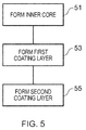
- Fig. 5 illustrates a method which may be used to form a composite particle 1 as described above.
- the method comprises, at block 51, forming an inner core 3 comprising a dielectric material.
- the method also comprises, at block 53, forming a first coating layer 5 overlaying the inner core 3 and at block 55 forming a second coating layer 7 overlaying the first coating layer 5 where the second coating layer 5 comprises a semi-conductor material.
- the first coating layer 5 comprises a plasmonic material configured to enable surface plasmons to be generated at a boundary 4 between the inner core 3 and the first coating layer 5 and a boundary 6 between the first coating layer 5 and the second coating layer 7.
- Examples of the disclosure provide a composite particle 1 which can be used to detect light or other electromagnetic radiation.
- the composite structure as described above improves the overall absorption efficiency of the nanoparticle.
- the composite structure also allows for tuning of the resonance of the surface plasmons which tunes the frequency of light, or other electromagnetic radiation, that is detected.
- the increase in the absorption cross section effectively traps more light within the composite particle and so increases the absorption of light by the second coating layer 7. This increases the amount of excitons created in the second coating layer 7.
- the creation of excitons may be improved by tuning the plasmon resonance to correspond to the exciton generation wavelength of the second coating layer 7.
- the composite particle 1 comprises an inner core 3 which could comprise a dielectric material such as polystyrene this reduces the volume of metals such as gold, silver and platinum which are required.
- example or “for example” or “may” in the text denotes, whether explicitly stated or not, that such features or functions are present in at least the described example, whether described as an example or not, and that they can be, but are not necessarily, present in some of or all other examples.
- example “for example” or “may” refers to a particular instance in a class of examples.
- a property of the instance can be a property of only that instance or a property of the class or a property of a subclass of the class that includes some but not all of the instances in the class. It is therefore implicitly disclosed that a features described with reference to one example but not with reference to another example, can where possible be used in that other example but does not necessarily have to be used in that other example.
Landscapes
- Light Receiving Elements (AREA)
- Investigating, Analyzing Materials By Fluorescence Or Luminescence (AREA)
Abstract

Description
- Examples of the disclosure relate to a composite particle, apparatus comprising a composite particle and method of producing a composite particle and apparatus. In particular, they relate to a composite particle, apparatus comprising a composite particle and method of producing a composite particle and apparatus which enable electromagnetic radiation to be detected.
- Apparatus for detecting electromagnetic radiation such as light is known. It is useful to improve the efficiency of such apparatus. It may also be useful to tune the wavelengths of the light, or other electromagnetic radiation that is detected.
- According to various, but not necessarily all, examples of the disclosure there is provided a composite particle comprising: an inner core comprising a dielectric material; a first coating layer provided overlaying the inner core; a second coating layer provided overlaying the first coating layer where the second coating layer comprises a semi-conductor material; and wherein the first coating layer comprises a plasmonic material configured to enable surface plasmons to be generated at a boundary between the inner core and the first coating layer and a boundary between the first coating layer and the second coating layer.
- In some examples the thickness of the first coating layer may enable coupling between surface plasmons generated at the boundary between the inner core and the first coating layer and surface plasmons generated at the boundary between the first coating layer and the second coating layer.
- In some examples the thickness of the first coating layer may be configured to tune the coupling of the surface plasmons so that the frequency of light absorbed by the first coating layer corresponds to the frequency of light absorbed by the second coating layer.
- In some examples the second coating layer may form the outer surface of the composite particle.
- In some examples the second coating layer may be configured to generate excitons in response to incident light.
- In some examples the inner core may comprise a material which does not absorb incident light.
- In some examples the inner core may comprise polystyrene.
- In some examples the first coating layer may comprise a metal.
- In some examples the composite particle may be spherical.
- According to various, but not necessarily all, examples of the disclosure there is provided an apparatus comprising at least one composite particle as described above and a layer of two dimensional material wherein the one or more composite particles are coupled to the layer of two dimensional material to enable absorption of light by the composite particle to be detected by the layer of two dimensional material.
- In some examples the two dimensional material may be configured to detect a change in the electric field of the composite particle caused by the absorption of light.
- In some examples the two dimensional material may form a channel within a field effect transistor.
- In some examples the two dimensional material may comprise graphene.
- According to various, but not necessarily all, examples of the disclosure there is provided a photodetector comprising at least one composite particle as described above.
- According to various, but not necessarily all, examples of the disclosure there is provided a photodetector comprising an apparatus as described above.
- According to various, but not necessarily all, examples of the disclosure there is provided a method comprising: forming an inner core comprising a dielectric material; forming a first coating layer overlaying the inner core; forming a second coating layer overlaying the first coating layer where the second coating layer comprises a semi-conductor material; and wherein the first coating layer comprises a plasmonic material configured to enable surface plasmons to be generated at a boundary between the inner core and the first coating layer and a boundary between the first coating layer and the second coating layer and wherein the inner core, first coating layer and second coating layer form a composite particle.
- In some examples the thickness of the first coating layer may enable coupling between surface plasmons generated at the boundary between the inner core and the first coating layer and surface plasmons generated at the boundary between the first coating layer and the second coating layer.
- In some examples the thickness of the first coating layer may be configured to tune the coupling of the surface plasmons so that the frequency of light absorbed by the first coating layer corresponds to the frequency of light absorbed by the second coating layer.
- In some examples the second coating layer may form the outer surface of the composite particle.
- In some examples the second coating layer may be configured to generate excitons in response to incident light.
- In some examples the inner core may comprise a material which does not absorb incident light.
- In some examples the inner core may comprise polystyrene.
- In some examples the first coating layer may comprise a metal.
- In some examples the inner core, first coating layer and second coating layer may form a spherical composite particle.
- In some examples the method may comprise coupling at least one composite particle as described above to a layer of two dimensional material to enable absorption of light by the composite particle to be detected by the layer of two dimensional material.
- In some examples the method may comprise configuring the two dimensional material to detect a change in the electric field of the composite particle caused by the absorption of light.
- In some examples the two dimensional material may be configured to form a channel within a field effect transistor.
- In some examples the two dimensional material comprises graphene.
- According to various, but not necessarily all, examples of the disclosure, there may be provided examples as claimed in the appended claims.
- For a better understanding of various examples that are useful for understanding the detailed description, reference will now be made by way of example only to the accompanying drawings in which:
-
Fig. 1 illustrates a composite particle; -
Fig. 2 illustrates an example photodetector comprising composite particles; -
Fig. 3 illustrates a plot of light absorbed by example composite particles; -
Fig. 4 illustrates another plot of light absorbed by example composite particles; and -
Fig. 5 illustrates a method. - The Figures illustrate a
composite particle 1 comprising: aninner core 3 comprising a dielectric material; afirst coating layer 5 provided overlaying theinner core 3; asecond coating layer 7 provided overlaying thefirst coating layer 5 where thesecond coating layer 7 comprises a semi-conductor material; and wherein thefirst coating layer 5 comprises a plasmonic material configured to enable surface plasmons to be generated at aboundary 4 between theinner core 3 and thefirst coating layer 5 and a boundary 6 between thefirst coating layer 5 and thesecond coating layer 7. - The
composite particle 1 may be for detecting light or other electromagnetic radiation. Thecomposite particle 1 may be used within photodetector devices, such as field effect transistors, to provide an electrical output signal indicative of the light or other electromagnetic radiation detected by the composite particle. -
Fig. 1 illustrates acomposite particle 1 according to examples of the disclosure. Thecomposite particle 1 comprises aninner core 3, afirst coating layer 5 and asecond coating layer 7. - The
composite particle 1 may be a nanoparticle or quantum dot. Thecomposite particle 1 may have a size of the order of 10nm. The dimensions of thecomposite particle 1 that are used may depend on the wavelength of light, or other electromagnetic radiation, that is to be detected. The dimensions of thecomposite particle 1 may depend on the dimensions of the respective layers within thecomposite particle 1. - The
inner core 3 comprises the centre of thecomposite particle 1. Theinner core 3 may provide a central solid nucleus for thecomposite particle 1. Theinner core 3 may comprise a dielectric material. In some examples theinner core 3 may comprise a material which does not absorb light. Theinner core 3 may comprise polystyrene or any other suitable material. - The
first coating layer 5 may be provided overlaying theinner core 3. Thefirst coating layer 5 may be provided directly overlaying theinner core 3 so that there are no intervening components or layers between theinner core 3 and thefirst coating layer 5. Aboundary 4 is provided between theinner core 3 and thefirst coating layer 5. - The
first coating layer 5 may comprise a plasmonic material. The plasmonic material may comprise any material which may create surface plasmons when incident light, or other electromagnetic radiation, is absorbed. The plasmonic material may comprise a metal such as gold, silver, nickel, platinum or any other suitable material. - The
first coating layer 5 may be arranged to increase the absorption of light by thesecond coating layer 7. - The material that is chosen for use as the
first coating layer 5 may depend on the wavelength of the light or other electromagnetic radiation that is to be detected. - The
second coating layer 7 may be provided overlaying thefirst coating layer 5. Thesecond coating layer 7 may be provided directly overlaying thefirst coating layer 5 so that there are no intervening components or layers between thefirst coating layer 5 and thesecond coating layer 7 and a boundary 6 is created between thefirst coating layer 5 and thesecond coating layer 7. - The
second coating layer 7 may provide the outer surface of thecomposite particle 1. Thesecond coating layer 7 may be configured so that excitons created within thesecond coating layer 7 and/or other changes in the electric field of thecomposite particle 1 can be detected by a two dimensional material. - In some examples the
second coating layer 7 may comprise a semiconducting material. The semiconducting material could comprise PbS, CdS, CdSe, Ge, ZnO, ZnS or any other suitable material. The material that is chosen for use as thesecond coating layer 7 may depend on the wavelength of the light or other electromagnetic radiation that is to be detected. - In the example of
Fig.1 thecomposite particle 1 is spherical. It is to be appreciated that other shaped particles may be used in other examples of the disclosure. For instance thecomposite particle 1 could be an elongate rod or any other suitable shape. The shape and size of thecomposite particle 1 could be chosen to tune the wavelength of light, or other electromagnetic radiation, that is absorbed by thecomposite particle 1. - The
composite particle 1 may be configured to absorb light, or other electromagnetic radiation, which is incident on thecomposite particle 1. Thecomposite particle 1 absorbs light using two different mechanisms. - The
second coating layer 7 absorbs light by exciton creation. Thesecond coating layer 7 comprises a semiconducting material which has a band gap between the valence band and the conducting band. If the light which is incident on thecomposite particle 1 has sufficient energy an electron will be excited within thesecond coating layer 7 from the valence band to the conduction band. This creates an exciton comprising an electron-hole pair. - The
second coating layer 7 may be thin so that any excitons generated can be detected by a transistor, or other suitable device, before the exciton recombines. If the thickness of thesecond coating layer 7 is increased this may increase the number of excitons created but the excitons may recombine within thesecond coating layer 7 before they can be detected. In some examples of the disclosure thesecond coating layer 7 may be several nanometers thick. Thesecond coating layer 7 may be less than 5nm thick. - The
composite particle 1 may also absorb light by the excitation of surface plasmons within thefirst coating layer 5. The surface plasmons are created by the interaction between the electromagnetic field of the incident light and the free electrons within the plasmonic material. - The excitation of localized surface plasmons by incident light, or other electromagnetic radiation, results in strong light scattering by the
composite particle 1, the appearance of intense surface plasmon absorption bands and an enhancement of the local electromagnetic fields of thecomposite particle 1. A localized surface plasmon resonance is generated when the wavelength of the incident light on thecomposite particle 1 is in resonance with an eigenmode of the surface plasmon resonance for thecomposite particle 1. From Mie scattering theory, the resonance condition for the extinction cross-section for an incident plane wave on a nanoparticle comprising a material, such as metal, is satisfied when
- Where εmetal is the dielectric constant of the metal and the ε diel is the dielectric constant of the material which forms the boundary with the plasmonic material. χ is a factor which depends on the geometry of the nanoparticle. The value of χ is 2 for a sphere but will be different for other shapes of particles. For instance, for nanorods with a high aspect ratio the value of χ could be as large as 20.
- This equation shows that materials which possess a negative real and small positive imaginary dielectric constant are capable of supporting surface plasmons. Suitable materials comprise gold, silver and platinum. However the conditions for generating the surface plasmons are only satisfied if the plasmonic material forms a boundary with a material which has a smaller magnitude for the real dielectric constant. In the examples of the disclosure the plasmonic material in the
second coating layer 5forms boundaries 4, 6 with a dielectric material in theinner core 3 and a semiconducting material insecond coating layer 7. This enables the surface plasmon resonances to be generated on both the inner and outer surface of thefirst coating layer 5. - In the examples of the disclosure the
composite particle 1 comprises afirst boundary 4 between theinner core 3 and thefirst coating layer 5 and a second boundary 6 between thefirst coating layer 5 and thesecond coating layer 7. When thecomposite particle 1 is illuminated the incident light generates a first surface plasmon at thefirst boundary 4 and a second surface plasmon at the second boundary 6. The two surface plasmons may interact to provide a single surface plasmon resonance. - The thickness of the
first coating layer 5 determines the magnitude of the coupling between the surface plasmons at thedifferent boundaries 4, 6. A thinner shell will provide for increased coupling between the surface plasmons and will effectively red shift the light absorbed by thefirst coating layer 5. The thickness of thefirst coating layer 5 may be selected to enable coupling between the surface plasmon generated at thefirst boundary 4 and the surface plasmon generated at the second boundary 6. This coupling between the surface plasmons on the respective boundaries changes the energy levels of the surface plasmons and effectively tunes the wavelength of light or other electromagnetic radiation that is absorbed by thecomposite particle 1. - The thickness of the
first coating layer 5 may be configured to tune the coupling of the surface plasmons so that the frequency of light absorbed by thefirst coating layer 5 corresponds to the frequency of light absorbed by the generation of excitons in thesecond coating layer 7. - Having the
multiple coating layers composite particle 1 increases the overall absorption cross section of thecomposite particle 1. Thesecond coating layer 5 can also be configured to tune the frequency of the plasmonic resonance by controlling the thickness of thefirst coating layer 5 and/or the materials used for the coating layer and/or the shape of thecomposite particle 1 and/or any other suitable factor. - Improving the absorption of light by the
first coating layer 5 also increases the absorption of light by thesecond coating layer 7. If the resonance of the surface plasmons is tuned to the wavelength for generating excitons this increases the number of excitons produced in thesecond coating layer 7. Thefirst coating layer 5 acts as a trap for light which then increases the amount of light absorbed by thesecond coating layer 7. This increases the overall absorption cross section of thecomposite particle 1 and improves the efficiency of thecomposite particle 1 at detecting light or other electromagnetic radiation. - The
composite particle 1 may be for use in any environment in which light, or other electromagnetic radiation, is to be detected. Thecomposite particle 1 may be suitable for use in a gaseous or liquid environment. - The
composite particle 1 may be coupled to any means which may enable the absorption of the light to be detected. In some examples thecomposite particle 1 may be coupled to a layer of two dimensional material to enable the absorption of light by thecomposite particle 1 to be detected. In such examples the two dimensional material may be configured to detect a change in the electric field or other properties of thecomposite particle 1 caused by the absorption of light by thecomposite particle 1. The two dimensional material could comprise any suitable material such graphene. -
Fig. 2 illustrates an example photodetector comprisingcomposite particles 1. In the example ofFig. 2 the photodetector comprises afield effect transistor 21. Other types of photodetector may be used in other examples of the disclosure. For instance thecomposite particles 1 may be used in any photo-sensitive devices such as photodiodes, photovoltaic devices or any other suitable devices. - The
field effect transistor 21 comprises asource electrode 23 and adrain electrode 24 and agraphene channel 25 between thesource electrode 23 and thedrain electrode 24. Thesource electrode 23 and thedrain electrode 24 may enable direct current to be provided to thegraphene channel 25. Theelectrodes - The
field effect transistor 21 also comprises alayer 27 ofcomposite particles 1. Thelayer 27 ofcomposite particles 1 provides a photoactive layer within thefield effect transistor 21. Thelayer 27 may comprise a plurality ofcomposite particles 1. Thelayer 27 may comprise several millioncomposite particles 1. Thelayer 27 ofcomposite particles 1 may be several hundred nanometers thick. In some examples thelayer 27 ofcomposite particles 1 may be between 5 and 1000nm thick. In some examples thelayer 27 ofcomposite particles 1 may be between 100 and 400nm thick. - The
layer 27 ofcomposite particles 1 is provided overlaying thegraphene channel 25. Thelayer 27 ofcomposite particles 1 may be coupled to thegraphene channel 25 so that a change in the electromagnetic field of thecomposite particles 1 within thelayer 27 is detected by thegraphene channel 25. Thelayer 27 ofcomposite particles 1 may be arranged to act as a gate electrode for thegraphene channel 25. - In some examples the
composite particles 1 may be coupled to thegraphene channel 25 so that charges generated by incident light are transferred to thegraphene channel 25. This increases the number of charge carriers within thegraphene channel 25 and so increases the conductivity of thegraphene channel 25. In some examples the absorption of the incident light may result in a change in the electric field of thecomposite particle 1. Thecomposite particles 1 may be positioned so that this change in electric field may affect the mobility of charges within thegraphene channel 25 and so may produce a detectable change in the conductivity of thegraphene channel 25. - In the example of
Fig. 2 thefield effect transistor 21 also comprises asubstrate 28. Thesubstrate 28 may support thesource electrode 23,drain electrode 24 and thegraphene channel 25. Thesubstrate 28 may also support connections to thesource electrode 23 anddrain electrode 24. Other components may be provided on thesubstrate 28. Thesubstrate 28 may comprise an insulating material such as glass or polymer or any other suitable material. - In the example of
Fig. 2 thefield effect transistor 21 also comprises apassivation layer 29. Thepassivation layer 29 may be configured to coat thetransistor 21 and protect it from environmental parameters. Thepassivation layer 29 may encapsulate the components of thetransistor 21. Thepassivation layer 29 may be transparent to the light, or other electromagnetic radiation, which is to be detected. For instance, in the example ofFig. 2 thepassivation layer 29 may allow visible light to pass through but may be configured to prevent fluids or other contaminants from reaching thetransistor 21. - In the example of
Fig. 2 thefield effect transistor 21 comprises agraphene channel 25. Other materials may be used for the channel in other examples of the disclosure. - When light, or other electromagnetic radiation is incident upon the
transistor 21 this causes absorption of light by thecomposite particles 1 within thelayer 27. This causes the generation of excitons within thesecond coating layer 7. The generation of excitons within thesecond coating layer 7 is enhanced by theinner core 3 andfirst coating layer 5. The electron hole pair may be split so that one of the charges preferentially conducts within thecomposite particle 1 while the other charge conducts with a slower mobility. The electric field within thefield effect transistor 21 may promote the transport of one charge compared to the other. - The
layer 27 ofcomposite particles 1 is arranged to enable charge to be transferred to thegraphene channel 25. As graphene has a high charge mobility this enables the charge to be transferred through thegraphene channel 25 before recombination can occur. This charge transfer causes a change in the current within thegraphene channel 25. In some examples the charge transfer may increase the number of dominant charge carriers within thegraphene channel 25. In some examples the charge transfer may cause recombination with the dominant charge carrier in thegraphene channel 25 which may decrease the number of dominant charge carriers. - The remaining charge from the excitons is trapped within the
composite particle 1 and acts to change the electric field around thecomposite particle 1. This change in the electric field also changes the conductivity of thegraphene channel 25. - The generation of the surface plasmons within the
first coating layer 5 may also change the electric field around thecomposite particle 1. This change in the electric field may also be detected as a change in the conductivity of thegraphene channel 25. -
Fig. 3 illustrates absorption spectra for an examplecomposite particle 1. The plot ofFig. 3 shows aplot 31 of acomposite particle 1 according to examples of the disclosure in comparison with aplot 33 of aPbS particle 35. - To obtain the data of
Fig. 3 thecomposite particle 1 was spherical and comprised aninner core 3 comprising polystyrene and having a radius of 3nm. Thefirst coating layer 5 comprised a gold layer which was 3nm thick. Theouter coating layer 7 comprised PbS and was 2nm thick. This gave thecomposite particle 1 an overall radius of 8nm. Other dimensions and materials for thecomposite particle 1 could be used in other examples of the disclosure. - To obtain the data for the plot in
Fig. 3 thePbS particle 35 had the same outer radius as thecomposite particle 1 and both of theparticles - The
plots solid PbS particle 35. -
Fig. 3 shows no discernible absorption peak in theplot 33 for thesolid PbS particle 35. This is not the case for theplot 31 of thecomposite particle 1 which shows a strong absorption peak at a wavelength of approximately 750nm. The improved absorption may be a direct result of the interaction between the surface plasmons on thefirst boundary 4 and the surface plasmons on the second boundary 6. The wavelength of the absorption peak could be tuned by modifying the dimensions of any one or more of theinner core 3, thefirst coating layer 5 or thesecond coating layer 7 or the materials used for any of these layers or the shape of thecomposite particle 1. -
Fig. 3 does not show any absorption peak due to excitons. To obtain the data for the plots ofFig. 3 the absorption cross-sections were calculated using the classical physics behavior of the PbS, polystyrene and Au dielectric properties alone. There was no consideration of the excitation of the quantum mechanical exciton in the PbS. If such mechanism were taken into account this would produce a small exciton peak at a wavelength above 1000 nm. These wavelengths are not included in the plot ofFig. 3 . -
Fig. 4 illustrates another absorption spectra for an examplecomposite particle 1. The plot ofFig. 4 shows aplot 31 of acomposite particle 1 according to examples of the disclosure in comparison with aplot 33 of aPbS particle 35. Theplots Fig. 3 and corresponding reference numerals have been used. -
Fig. 4 also shows aplot 41 for anotherparticle 43 comprising a gold core 45 and a PbS outer coating 47. To obtain the data used inFig. 4 the gold core 45 was spherical and had a radius of 6nm and the PbS outer coating 47 had a thickness of 2nm. This gave theparticle 43 an overall radius of 8nm which is the same as the radius for thecomposite particle 1 and thePbS particle 33. - The
plot 41 for theparticle 43 has an absorption peak between 600 and 700nm. The peak in theplot 41 is smaller than the peak in theplot 31 for thecomposite particle 1. Therefore it can be seen that the composite particle structure of the examples of the disclosure of the invention increases the absorption of the particles. This also shows that the composite particle shifts the wavelength at which the peak occurs. This structure of the composite particle enables the wavelength at which the absorption peak occurs to be controlled. -
Fig. 5 illustrates a method which may be used to form acomposite particle 1 as described above. The method comprises, atblock 51, forming aninner core 3 comprising a dielectric material. The method also comprises, atblock 53, forming afirst coating layer 5 overlaying theinner core 3 and atblock 55 forming asecond coating layer 7 overlaying thefirst coating layer 5 where thesecond coating layer 5 comprises a semi-conductor material. Thefirst coating layer 5 comprises a plasmonic material configured to enable surface plasmons to be generated at aboundary 4 between theinner core 3 and thefirst coating layer 5 and a boundary 6 between thefirst coating layer 5 and thesecond coating layer 7. - Examples of the disclosure provide a
composite particle 1 which can be used to detect light or other electromagnetic radiation. The composite structure as described above improves the overall absorption efficiency of the nanoparticle. The composite structure also allows for tuning of the resonance of the surface plasmons which tunes the frequency of light, or other electromagnetic radiation, that is detected. - The increase in the absorption cross section effectively traps more light within the composite particle and so increases the absorption of light by the
second coating layer 7. This increases the amount of excitons created in thesecond coating layer 7. The creation of excitons may be improved by tuning the plasmon resonance to correspond to the exciton generation wavelength of thesecond coating layer 7. - As the
composite particle 1 comprises aninner core 3 which could comprise a dielectric material such as polystyrene this reduces the volume of metals such as gold, silver and platinum which are required. - The term "comprise" is used in this document with an inclusive not an exclusive meaning. That is any reference to X comprising Y indicates that X may comprise only one Y or may comprise more than one Y. If it is intended to use "comprise" with an exclusive meaning then it will be made clear in the context by referring to "comprising only one..." or by using "consisting".
- In this detailed description, reference has been made to various examples. The description of features or functions in relation to an example indicates that those features or functions are present in that example. The use of the term "example" or "for example" or "may" in the text denotes, whether explicitly stated or not, that such features or functions are present in at least the described example, whether described as an example or not, and that they can be, but are not necessarily, present in some of or all other examples. Thus "example", "for example" or "may" refers to a particular instance in a class of examples. A property of the instance can be a property of only that instance or a property of the class or a property of a subclass of the class that includes some but not all of the instances in the class. It is therefore implicitly disclosed that a features described with reference to one example but not with reference to another example, can where possible be used in that other example but does not necessarily have to be used in that other example.
- Although embodiments of the present invention have been described in the preceding paragraphs with reference to various examples, it should be appreciated that modifications to the examples given can be made without departing from the scope of the invention as claimed.
- Features described in the preceding description may be used in combinations other than the combinations explicitly described.
- Although functions have been described with reference to certain features, those functions may be performable by other features whether described or not.
- Although features have been described with reference to certain embodiments, those features may also be present in other embodiments whether described or not.
- Whilst endeavoring in the foregoing specification to draw attention to those features of the invention believed to be of particular importance it should be understood that the Applicant claims protection in respect of any patentable feature or combination of features hereinbefore referred to and/or shown in the drawings whether or not particular emphasis has been placed thereon.
Claims (15)
- A composite particle comprising:an inner core comprising a dielectric material;a first coating layer provided overlaying the inner core;a second coating layer provided overlaying the first coating layer where the second coating layer comprises a semi-conductor material; andwherein the first coating layer comprises a plasmonic material configured to enable surface plasmons to be generated at a boundary between the inner core and the first coating layer and a boundary between the first coating layer and the second coating layer.
- A composite particle as claimed in any preceding claim wherein the thickness of the first coating layer enables coupling between surface plasmons generated at the boundary between the inner core and the first coating layer and surface plasmons generated at the boundary between the first coating layer and the second coating layer.
- A composite particle as claimed in claim 2 wherein the thickness of the first coating layer is configured to tune the coupling of the surface plasmons so that the frequency of light absorbed by the first coating layer corresponds to the frequency of light absorbed by the second coating layer.
- A composite particle as claimed in any preceding claim wherein the second coating layer forms the outer surface of the composite particle.
- A composite particle as claimed in any preceding claim wherein the second coating layer is configured to generate excitons in response to incident light.
- A composite particle as claimed in any preceding claim wherein the inner core comprises a material which does not absorb incident light.
- A composite particle as claimed in any preceding claim wherein the inner core comprises polystyrene.
- A composite particle as claimed in any preceding claim wherein the first coating layer comprises a metal.
- A composite particle as claimed in any preceding claim wherein the composite particle is spherical.
- An apparatus comprising at least one composite particle as claimed in any of claims 1 to 9 and a layer of two dimensional material wherein the one or more composite particles are coupled to the layer of two dimensional material to enable absorption of light by the composite particle to be detected by the layer of two dimensional material.
- An apparatus as claimed in claim 10 wherein the two dimensional material is configured to detect a change in the electric field of the composite particle caused by the absorption of light.
- An apparatus as claimed in any of claims 10 to 11 wherein the two dimensional material forms a channel within a field effect transistor.
- An apparatus as claimed in any of claims 10 to 12 wherein the two dimensional material comprises graphene.
- A photodetector comprising at least one of; at least one composite particle as claimed in any of claims 1 to 9, an apparatus as claimed in any of claims 10 to 13.
- A method comprising:forming an inner core comprising a dielectric material;forming a first coating layer overlaying the inner core;forming a second coating layer overlaying the first coating layer where the second coating layer comprises a semi-conductor material; andwherein the first coating layer comprises a plasmonic material configured to enable surface plasmons to be generated at a boundary between the inner core and the first coating layer and a boundary between the first coating layer and the second coating layer and wherein the inner core, first coating layer and second coating layer form a composite particle.
Priority Applications (3)
| Application Number | Priority Date | Filing Date | Title |
|---|---|---|---|
| EP16150795.9A EP3190632B1 (en) | 2016-01-11 | 2016-01-11 | A composite nanoparticle and photodetector comprising the nanoparticle |
| US16/068,704 US10541347B2 (en) | 2016-01-11 | 2016-12-28 | Composite nanoparticle and photodetector comprising the nanoparticle |
| PCT/FI2016/050926 WO2017121922A1 (en) | 2016-01-11 | 2016-12-28 | A composite nanoparticle and photodetector comprising the nanoparticle |
Applications Claiming Priority (1)
| Application Number | Priority Date | Filing Date | Title |
|---|---|---|---|
| EP16150795.9A EP3190632B1 (en) | 2016-01-11 | 2016-01-11 | A composite nanoparticle and photodetector comprising the nanoparticle |
Publications (2)
| Publication Number | Publication Date |
|---|---|
| EP3190632A1 true EP3190632A1 (en) | 2017-07-12 |
| EP3190632B1 EP3190632B1 (en) | 2021-05-05 |
Family
ID=55129564
Family Applications (1)
| Application Number | Title | Priority Date | Filing Date |
|---|---|---|---|
| EP16150795.9A Active EP3190632B1 (en) | 2016-01-11 | 2016-01-11 | A composite nanoparticle and photodetector comprising the nanoparticle |
Country Status (3)
| Country | Link |
|---|---|
| US (1) | US10541347B2 (en) |
| EP (1) | EP3190632B1 (en) |
| WO (1) | WO2017121922A1 (en) |
Cited By (1)
| Publication number | Priority date | Publication date | Assignee | Title |
|---|---|---|---|---|
| JPWO2023037797A1 (en) * | 2021-09-10 | 2023-03-16 |
Citations (2)
| Publication number | Priority date | Publication date | Assignee | Title |
|---|---|---|---|---|
| WO1999046351A1 (en) * | 1998-03-11 | 1999-09-16 | Wm. Marsh Rice University | Metal nanoshells |
| US20140299741A1 (en) * | 2013-04-05 | 2014-10-09 | Nokia Corporation | Transparent Photodetector for Mobile Devices |
Family Cites Families (5)
| Publication number | Priority date | Publication date | Assignee | Title |
|---|---|---|---|---|
| AU2002246587A1 (en) | 2000-11-03 | 2002-08-06 | Wm. Marsh Rice University | Partial coverage metal nanoshells and method of making same |
| JP4528927B2 (en) | 2003-09-04 | 2010-08-25 | 独立行政法人産業技術総合研究所 | Composite fine particle production method, composite fine particle production apparatus, and composite fine particle |
| US20080241262A1 (en) | 2004-03-29 | 2008-10-02 | The University Of Houston System | Nanoshells and Discrete Polymer-Coated Nanoshells, Methods For Making and Using Same |
| US7790066B2 (en) | 2006-03-03 | 2010-09-07 | William Marsh Rice University | Nanorice particles: hybrid plasmonic nanostructures |
| US8598567B2 (en) | 2010-05-17 | 2013-12-03 | University Of Washington Through Its Center For Commercialization | Color-selective quantum dot photodetectors |
-
2016
- 2016-01-11 EP EP16150795.9A patent/EP3190632B1/en active Active
- 2016-12-28 WO PCT/FI2016/050926 patent/WO2017121922A1/en not_active Ceased
- 2016-12-28 US US16/068,704 patent/US10541347B2/en active Active
Patent Citations (2)
| Publication number | Priority date | Publication date | Assignee | Title |
|---|---|---|---|---|
| WO1999046351A1 (en) * | 1998-03-11 | 1999-09-16 | Wm. Marsh Rice University | Metal nanoshells |
| US20140299741A1 (en) * | 2013-04-05 | 2014-10-09 | Nokia Corporation | Transparent Photodetector for Mobile Devices |
Non-Patent Citations (6)
| Title |
|---|
| AKRAM KHOSROABADI ET AL: "Nanoimprinted Hybrid Metal-Semiconductor Plasmonic Multilayers with Controlled Surface Nano Architecture for Applications in NIR Detectors", MATERIALS, vol. 8, no. 8, 7 August 2015 (2015-08-07), pages 5028 - 5047, XP055293716, DOI: 10.3390/ma8085028 * |
| ALY OKASHA ET AL: "Weak exciton-plasmon and exciton-phonon coupling in chemically synthesized Ag/CdSe metal/semiconductor hybrid nanocomposite", PHYSICA E - LOW-DIMENSIONAL SYSTEMS AND NANOSTRUCTURES, vol. 44, no. 10, 4 July 2012 (2012-07-04), NL, pages 2094 - 2098, XP055294259, ISSN: 1386-9477, DOI: 10.1016/j.physe.2012.06.022 * |
| GERASIMOS KONSTANTATOS ET AL: "Hybrid graphene-quantum dot phototransistors with ultrahigh gain", NATURE NANOTECHNOLOGY, vol. 7, no. 6, 1 January 2012 (2012-01-01), pages 363 - 368, XP055039980, ISSN: 1748-3387, DOI: 10.1038/nnano.2012.60 * |
| KATSUAKI TANABE: "Field Enhancement around Metal Nanoparticles and Nanoshells: A Systematic Investigation", JOURNAL OF PHYSICAL CHEMISTRY C, vol. 112, no. 40, 13 September 2008 (2008-09-13), US, pages 15721 - 15728, XP055293715, ISSN: 1932-7447, DOI: 10.1021/jp8060009 * |
| RUIBIN JIANG ET AL: "Metal/Semiconductor Hybrid Nanostructures for Plasmon-Enhanced Applications", ADVANCED MATERIALS, vol. 26, no. 31, 19 April 2014 (2014-04-19), DE, pages 5274 - 5309, XP055293714, ISSN: 0935-9648, DOI: 10.1002/adma.201400203 * |
| YONG K T ET AL: "Synthesis and plasmonic properties of silver and gold nanoshells on polystyrene cores of different size and of gold-silver core-shell nanostructures", COLLOIDS AND SURFACES. A, PHYSICACHEMICAL AND ENGINEERING ASPECTS, ELSEVIER, AMSTERDAM, NL, vol. 290, no. 1-3, 15 November 2006 (2006-11-15), pages 89 - 105, XP027996183, ISSN: 0927-7757, [retrieved on 20061115] * |
Cited By (3)
| Publication number | Priority date | Publication date | Assignee | Title |
|---|---|---|---|---|
| JPWO2023037797A1 (en) * | 2021-09-10 | 2023-03-16 | ||
| JP7540801B2 (en) | 2021-09-10 | 2024-08-27 | 国立研究開発法人科学技術振興機構 | Composite microparticles, solar cells, photoelectric conversion element members, and photoelectric conversion elements |
| US12305101B2 (en) | 2021-09-10 | 2025-05-20 | Japan Science And Technology Agency | Composite fine particles, solar cell, member for photoelectric conversion elements, and photoelectric conversion element |
Also Published As
| Publication number | Publication date |
|---|---|
| US10541347B2 (en) | 2020-01-21 |
| US20190027631A1 (en) | 2019-01-24 |
| WO2017121922A1 (en) | 2017-07-20 |
| EP3190632B1 (en) | 2021-05-05 |
Similar Documents
| Publication | Publication Date | Title |
|---|---|---|
| Livache et al. | A colloidal quantum dot infrared photodetector and its use for intraband detection | |
| Jeong et al. | Air-stable n-doped colloidal HgS quantum dots | |
| Di Bartolomeo et al. | Electrical transport and persistent photoconductivity in monolayer MoS2 phototransistors | |
| Chen et al. | Synergistic effects of plasmonics and electron trapping in graphene short-wave infrared photodetectors with ultrahigh responsivity | |
| Pescaglini et al. | Hot-electron injection in Au nanorod–ZnO nanowire hybrid device for near-infrared photodetection | |
| Dhara et al. | Enhanced UV photosensitivity from rapid thermal annealed vertically aligned ZnO nanowires | |
| Nian et al. | Graphene/PbS-quantum dots/graphene sandwich structures enabled by laser shock imprinting for high performance photodetectors | |
| US10923612B2 (en) | Photodiode having quantum dot light absorption layer | |
| Lu et al. | ZnO quantum dot-doped graphene/h-BN/GaN-heterostructure ultraviolet photodetector with extremely high responsivity | |
| Zhang et al. | Optoelectronic response of a WS2 tubular p-n junction | |
| Nguyen et al. | Advances in graphene-based optoelectronics, plasmonics and photonics | |
| Novitsky et al. | Photon absorption and photocurrent in solar cells below semiconductor bandgap due to electron photoemission from plasmonic nanoantennas | |
| Paria et al. | Graphene–silver hybrid devices for sensitive photodetection in the ultraviolet | |
| Song et al. | Ultranarrow mid-infrared quantum plasmon resonance of self-doped silver selenide nanocrystal | |
| Wang et al. | Hybrid Si nanocones/PEDOT: PSS solar cell | |
| Li et al. | Substrate-induced interfacial plasmonics for photovoltaic conversion | |
| Sarkar et al. | Photoresponse characteristics of MoS2 QDs/Si nanocone heterojunctions utilizing geometry controlled light trapping mechanism in black Si | |
| Yu et al. | Hot‐carrier engineering for two‐dimensional integrated infrared optoelectronics | |
| US10593768B2 (en) | Apparatus comprising two dimensional material | |
| Taliashvili et al. | Optical properties of periodically and aperiodically nanostructured pn junctions | |
| Hong et al. | Design guideline of Si nanohole/PEDOT: PSS hybrid structure for solar cell application | |
| Jabeen et al. | 2D/3D graphene on h-BN interlayer-silicon solar cell with ZnO: Al buffer layer and enormous light captivation using Au/Ag NPs | |
| Švrček et al. | Stable ultrathin surfactant‐free surface‐engineered silicon nanocrystal solar cells deposited at room temperature | |
| EP3190632B1 (en) | A composite nanoparticle and photodetector comprising the nanoparticle | |
| Xia et al. | Effect of hydrogen and oxygen plasma on the photoelectronic current and photo-response time of SnS2 flakes |
Legal Events
| Date | Code | Title | Description |
|---|---|---|---|
| PUAI | Public reference made under article 153(3) epc to a published international application that has entered the european phase |
Free format text: ORIGINAL CODE: 0009012 |
|
| STAA | Information on the status of an ep patent application or granted ep patent |
Free format text: STATUS: THE APPLICATION HAS BEEN PUBLISHED |
|
| AK | Designated contracting states |
Kind code of ref document: A1 Designated state(s): AL AT BE BG CH CY CZ DE DK EE ES FI FR GB GR HR HU IE IS IT LI LT LU LV MC MK MT NL NO PL PT RO RS SE SI SK SM TR |
|
| AX | Request for extension of the european patent |
Extension state: BA ME |
|
| STAA | Information on the status of an ep patent application or granted ep patent |
Free format text: STATUS: REQUEST FOR EXAMINATION WAS MADE |
|
| 17P | Request for examination filed |
Effective date: 20180111 |
|
| RBV | Designated contracting states (corrected) |
Designated state(s): AL AT BE BG CH CY CZ DE DK EE ES FI FR GB GR HR HU IE IS IT LI LT LU LV MC MK MT NL NO PL PT RO RS SE SI SK SM TR |
|
| RAP1 | Party data changed (applicant data changed or rights of an application transferred) |
Owner name: NOKIA TECHNOLOGIES OY |
|
| GRAP | Despatch of communication of intention to grant a patent |
Free format text: ORIGINAL CODE: EPIDOSNIGR1 |
|
| STAA | Information on the status of an ep patent application or granted ep patent |
Free format text: STATUS: GRANT OF PATENT IS INTENDED |
|
| INTG | Intention to grant announced |
Effective date: 20201126 |
|
| GRAS | Grant fee paid |
Free format text: ORIGINAL CODE: EPIDOSNIGR3 |
|
| GRAA | (expected) grant |
Free format text: ORIGINAL CODE: 0009210 |
|
| STAA | Information on the status of an ep patent application or granted ep patent |
Free format text: STATUS: THE PATENT HAS BEEN GRANTED |
|
| AK | Designated contracting states |
Kind code of ref document: B1 Designated state(s): AL AT BE BG CH CY CZ DE DK EE ES FI FR GB GR HR HU IE IS IT LI LT LU LV MC MK MT NL NO PL PT RO RS SE SI SK SM TR |
|
| REG | Reference to a national code |
Ref country code: GB Ref legal event code: FG4D |
|
| REG | Reference to a national code |
Ref country code: CH Ref legal event code: EP |
|
| REG | Reference to a national code |
Ref country code: AT Ref legal event code: REF Ref document number: 1390917 Country of ref document: AT Kind code of ref document: T Effective date: 20210515 |
|
| REG | Reference to a national code |
Ref country code: DE Ref legal event code: R096 Ref document number: 602016057213 Country of ref document: DE |
|
| REG | Reference to a national code |
Ref country code: IE Ref legal event code: FG4D |
|
| REG | Reference to a national code |
Ref country code: LT Ref legal event code: MG9D |
|
| REG | Reference to a national code |
Ref country code: AT Ref legal event code: MK05 Ref document number: 1390917 Country of ref document: AT Kind code of ref document: T Effective date: 20210505 |
|
| PG25 | Lapsed in a contracting state [announced via postgrant information from national office to epo] |
Ref country code: LT Free format text: LAPSE BECAUSE OF FAILURE TO SUBMIT A TRANSLATION OF THE DESCRIPTION OR TO PAY THE FEE WITHIN THE PRESCRIBED TIME-LIMIT Effective date: 20210505 Ref country code: FI Free format text: LAPSE BECAUSE OF FAILURE TO SUBMIT A TRANSLATION OF THE DESCRIPTION OR TO PAY THE FEE WITHIN THE PRESCRIBED TIME-LIMIT Effective date: 20210505 Ref country code: BG Free format text: LAPSE BECAUSE OF FAILURE TO SUBMIT A TRANSLATION OF THE DESCRIPTION OR TO PAY THE FEE WITHIN THE PRESCRIBED TIME-LIMIT Effective date: 20210805 Ref country code: AT Free format text: LAPSE BECAUSE OF FAILURE TO SUBMIT A TRANSLATION OF THE DESCRIPTION OR TO PAY THE FEE WITHIN THE PRESCRIBED TIME-LIMIT Effective date: 20210505 Ref country code: HR Free format text: LAPSE BECAUSE OF FAILURE TO SUBMIT A TRANSLATION OF THE DESCRIPTION OR TO PAY THE FEE WITHIN THE PRESCRIBED TIME-LIMIT Effective date: 20210505 |
|
| PG25 | Lapsed in a contracting state [announced via postgrant information from national office to epo] |
Ref country code: IS Free format text: LAPSE BECAUSE OF FAILURE TO SUBMIT A TRANSLATION OF THE DESCRIPTION OR TO PAY THE FEE WITHIN THE PRESCRIBED TIME-LIMIT Effective date: 20210905 Ref country code: GR Free format text: LAPSE BECAUSE OF FAILURE TO SUBMIT A TRANSLATION OF THE DESCRIPTION OR TO PAY THE FEE WITHIN THE PRESCRIBED TIME-LIMIT Effective date: 20210806 Ref country code: LV Free format text: LAPSE BECAUSE OF FAILURE TO SUBMIT A TRANSLATION OF THE DESCRIPTION OR TO PAY THE FEE WITHIN THE PRESCRIBED TIME-LIMIT Effective date: 20210505 Ref country code: SE Free format text: LAPSE BECAUSE OF FAILURE TO SUBMIT A TRANSLATION OF THE DESCRIPTION OR TO PAY THE FEE WITHIN THE PRESCRIBED TIME-LIMIT Effective date: 20210505 Ref country code: RS Free format text: LAPSE BECAUSE OF FAILURE TO SUBMIT A TRANSLATION OF THE DESCRIPTION OR TO PAY THE FEE WITHIN THE PRESCRIBED TIME-LIMIT Effective date: 20210505 Ref country code: PL Free format text: LAPSE BECAUSE OF FAILURE TO SUBMIT A TRANSLATION OF THE DESCRIPTION OR TO PAY THE FEE WITHIN THE PRESCRIBED TIME-LIMIT Effective date: 20210505 Ref country code: PT Free format text: LAPSE BECAUSE OF FAILURE TO SUBMIT A TRANSLATION OF THE DESCRIPTION OR TO PAY THE FEE WITHIN THE PRESCRIBED TIME-LIMIT Effective date: 20210906 Ref country code: NO Free format text: LAPSE BECAUSE OF FAILURE TO SUBMIT A TRANSLATION OF THE DESCRIPTION OR TO PAY THE FEE WITHIN THE PRESCRIBED TIME-LIMIT Effective date: 20210805 |
|
| REG | Reference to a national code |
Ref country code: NL Ref legal event code: MP Effective date: 20210505 |
|
| PG25 | Lapsed in a contracting state [announced via postgrant information from national office to epo] |
Ref country code: NL Free format text: LAPSE BECAUSE OF FAILURE TO SUBMIT A TRANSLATION OF THE DESCRIPTION OR TO PAY THE FEE WITHIN THE PRESCRIBED TIME-LIMIT Effective date: 20210505 |
|
| PG25 | Lapsed in a contracting state [announced via postgrant information from national office to epo] |
Ref country code: RO Free format text: LAPSE BECAUSE OF FAILURE TO SUBMIT A TRANSLATION OF THE DESCRIPTION OR TO PAY THE FEE WITHIN THE PRESCRIBED TIME-LIMIT Effective date: 20210505 Ref country code: ES Free format text: LAPSE BECAUSE OF FAILURE TO SUBMIT A TRANSLATION OF THE DESCRIPTION OR TO PAY THE FEE WITHIN THE PRESCRIBED TIME-LIMIT Effective date: 20210505 Ref country code: SK Free format text: LAPSE BECAUSE OF FAILURE TO SUBMIT A TRANSLATION OF THE DESCRIPTION OR TO PAY THE FEE WITHIN THE PRESCRIBED TIME-LIMIT Effective date: 20210505 Ref country code: SM Free format text: LAPSE BECAUSE OF FAILURE TO SUBMIT A TRANSLATION OF THE DESCRIPTION OR TO PAY THE FEE WITHIN THE PRESCRIBED TIME-LIMIT Effective date: 20210505 Ref country code: DK Free format text: LAPSE BECAUSE OF FAILURE TO SUBMIT A TRANSLATION OF THE DESCRIPTION OR TO PAY THE FEE WITHIN THE PRESCRIBED TIME-LIMIT Effective date: 20210505 Ref country code: CZ Free format text: LAPSE BECAUSE OF FAILURE TO SUBMIT A TRANSLATION OF THE DESCRIPTION OR TO PAY THE FEE WITHIN THE PRESCRIBED TIME-LIMIT Effective date: 20210505 Ref country code: EE Free format text: LAPSE BECAUSE OF FAILURE TO SUBMIT A TRANSLATION OF THE DESCRIPTION OR TO PAY THE FEE WITHIN THE PRESCRIBED TIME-LIMIT Effective date: 20210505 |
|
| REG | Reference to a national code |
Ref country code: DE Ref legal event code: R097 Ref document number: 602016057213 Country of ref document: DE |
|
| PLBE | No opposition filed within time limit |
Free format text: ORIGINAL CODE: 0009261 |
|
| STAA | Information on the status of an ep patent application or granted ep patent |
Free format text: STATUS: NO OPPOSITION FILED WITHIN TIME LIMIT |
|
| 26N | No opposition filed |
Effective date: 20220208 |
|
| PG25 | Lapsed in a contracting state [announced via postgrant information from national office to epo] |
Ref country code: IS Free format text: LAPSE BECAUSE OF FAILURE TO SUBMIT A TRANSLATION OF THE DESCRIPTION OR TO PAY THE FEE WITHIN THE PRESCRIBED TIME-LIMIT Effective date: 20210905 Ref country code: AL Free format text: LAPSE BECAUSE OF FAILURE TO SUBMIT A TRANSLATION OF THE DESCRIPTION OR TO PAY THE FEE WITHIN THE PRESCRIBED TIME-LIMIT Effective date: 20210505 |
|
| PG25 | Lapsed in a contracting state [announced via postgrant information from national office to epo] |
Ref country code: IT Free format text: LAPSE BECAUSE OF FAILURE TO SUBMIT A TRANSLATION OF THE DESCRIPTION OR TO PAY THE FEE WITHIN THE PRESCRIBED TIME-LIMIT Effective date: 20210505 |
|
| REG | Reference to a national code |
Ref country code: DE Ref legal event code: R119 Ref document number: 602016057213 Country of ref document: DE |
|
| PG25 | Lapsed in a contracting state [announced via postgrant information from national office to epo] |
Ref country code: MC Free format text: LAPSE BECAUSE OF FAILURE TO SUBMIT A TRANSLATION OF THE DESCRIPTION OR TO PAY THE FEE WITHIN THE PRESCRIBED TIME-LIMIT Effective date: 20210505 |
|
| REG | Reference to a national code |
Ref country code: CH Ref legal event code: PL |
|
| REG | Reference to a national code |
Ref country code: BE Ref legal event code: MM Effective date: 20220131 |
|
| PG25 | Lapsed in a contracting state [announced via postgrant information from national office to epo] |
Ref country code: LU Free format text: LAPSE BECAUSE OF NON-PAYMENT OF DUE FEES Effective date: 20220111 Ref country code: DE Free format text: LAPSE BECAUSE OF NON-PAYMENT OF DUE FEES Effective date: 20220802 |
|
| PG25 | Lapsed in a contracting state [announced via postgrant information from national office to epo] |
Ref country code: FR Free format text: LAPSE BECAUSE OF NON-PAYMENT OF DUE FEES Effective date: 20220131 Ref country code: BE Free format text: LAPSE BECAUSE OF NON-PAYMENT OF DUE FEES Effective date: 20220131 |
|
| PG25 | Lapsed in a contracting state [announced via postgrant information from national office to epo] |
Ref country code: LI Free format text: LAPSE BECAUSE OF NON-PAYMENT OF DUE FEES Effective date: 20220131 Ref country code: CH Free format text: LAPSE BECAUSE OF NON-PAYMENT OF DUE FEES Effective date: 20220131 |
|
| PG25 | Lapsed in a contracting state [announced via postgrant information from national office to epo] |
Ref country code: IE Free format text: LAPSE BECAUSE OF NON-PAYMENT OF DUE FEES Effective date: 20220111 |
|
| P01 | Opt-out of the competence of the unified patent court (upc) registered |
Effective date: 20230527 |
|
| PG25 | Lapsed in a contracting state [announced via postgrant information from national office to epo] |
Ref country code: HU Free format text: LAPSE BECAUSE OF FAILURE TO SUBMIT A TRANSLATION OF THE DESCRIPTION OR TO PAY THE FEE WITHIN THE PRESCRIBED TIME-LIMIT; INVALID AB INITIO Effective date: 20160111 |
|
| PG25 | Lapsed in a contracting state [announced via postgrant information from national office to epo] |
Ref country code: MK Free format text: LAPSE BECAUSE OF FAILURE TO SUBMIT A TRANSLATION OF THE DESCRIPTION OR TO PAY THE FEE WITHIN THE PRESCRIBED TIME-LIMIT Effective date: 20210505 Ref country code: CY Free format text: LAPSE BECAUSE OF FAILURE TO SUBMIT A TRANSLATION OF THE DESCRIPTION OR TO PAY THE FEE WITHIN THE PRESCRIBED TIME-LIMIT Effective date: 20210505 |
|
| PG25 | Lapsed in a contracting state [announced via postgrant information from national office to epo] |
Ref country code: TR Free format text: LAPSE BECAUSE OF FAILURE TO SUBMIT A TRANSLATION OF THE DESCRIPTION OR TO PAY THE FEE WITHIN THE PRESCRIBED TIME-LIMIT Effective date: 20210505 |
|
| PG25 | Lapsed in a contracting state [announced via postgrant information from national office to epo] |
Ref country code: MT Free format text: LAPSE BECAUSE OF FAILURE TO SUBMIT A TRANSLATION OF THE DESCRIPTION OR TO PAY THE FEE WITHIN THE PRESCRIBED TIME-LIMIT Effective date: 20210505 |
|
| PGFP | Annual fee paid to national office [announced via postgrant information from national office to epo] |
Ref country code: GB Payment date: 20251204 Year of fee payment: 11 |