EP3188245A1 - Finfet and fabrication method thereof - Google Patents
Finfet and fabrication method thereof Download PDFInfo
- Publication number
- EP3188245A1 EP3188245A1 EP16205796.2A EP16205796A EP3188245A1 EP 3188245 A1 EP3188245 A1 EP 3188245A1 EP 16205796 A EP16205796 A EP 16205796A EP 3188245 A1 EP3188245 A1 EP 3188245A1
- Authority
- EP
- European Patent Office
- Prior art keywords
- region
- semiconductor substrate
- punch
- hard mask
- mask layer
- Prior art date
- Legal status (The legal status is an assumption and is not a legal conclusion. Google has not performed a legal analysis and makes no representation as to the accuracy of the status listed.)
- Granted
Links
Images




Classifications
-
- H—ELECTRICITY
- H10—SEMICONDUCTOR DEVICES; ELECTRIC SOLID-STATE DEVICES NOT OTHERWISE PROVIDED FOR
- H10D—INORGANIC ELECTRIC SEMICONDUCTOR DEVICES
- H10D62/00—Semiconductor bodies, or regions thereof, of devices having potential barriers
- H10D62/10—Shapes, relative sizes or dispositions of the regions of the semiconductor bodies; Shapes of the semiconductor bodies
- H10D62/102—Constructional design considerations for preventing surface leakage or controlling electric field concentration
- H10D62/112—Constructional design considerations for preventing surface leakage or controlling electric field concentration for preventing surface leakage due to surface inversion layers, e.g. by using channel stoppers
-
- H—ELECTRICITY
- H10—SEMICONDUCTOR DEVICES; ELECTRIC SOLID-STATE DEVICES NOT OTHERWISE PROVIDED FOR
- H10D—INORGANIC ELECTRIC SEMICONDUCTOR DEVICES
- H10D30/00—Field-effect transistors [FET]
- H10D30/01—Manufacture or treatment
- H10D30/021—Manufacture or treatment of FETs having insulated gates [IGFET]
- H10D30/0217—Manufacture or treatment of FETs having insulated gates [IGFET] forming self-aligned punch-through stoppers or threshold implants under gate regions
-
- H—ELECTRICITY
- H10—SEMICONDUCTOR DEVICES; ELECTRIC SOLID-STATE DEVICES NOT OTHERWISE PROVIDED FOR
- H10D—INORGANIC ELECTRIC SEMICONDUCTOR DEVICES
- H10D30/00—Field-effect transistors [FET]
- H10D30/01—Manufacture or treatment
- H10D30/021—Manufacture or treatment of FETs having insulated gates [IGFET]
- H10D30/024—Manufacture or treatment of FETs having insulated gates [IGFET] of fin field-effect transistors [FinFET]
-
- H—ELECTRICITY
- H10—SEMICONDUCTOR DEVICES; ELECTRIC SOLID-STATE DEVICES NOT OTHERWISE PROVIDED FOR
- H10D—INORGANIC ELECTRIC SEMICONDUCTOR DEVICES
- H10D30/00—Field-effect transistors [FET]
- H10D30/01—Manufacture or treatment
- H10D30/021—Manufacture or treatment of FETs having insulated gates [IGFET]
- H10D30/024—Manufacture or treatment of FETs having insulated gates [IGFET] of fin field-effect transistors [FinFET]
- H10D30/0241—Manufacture or treatment of FETs having insulated gates [IGFET] of fin field-effect transistors [FinFET] doping of vertical sidewalls, e.g. using tilted or multi-angled implants
-
- H—ELECTRICITY
- H10—SEMICONDUCTOR DEVICES; ELECTRIC SOLID-STATE DEVICES NOT OTHERWISE PROVIDED FOR
- H10D—INORGANIC ELECTRIC SEMICONDUCTOR DEVICES
- H10D30/00—Field-effect transistors [FET]
- H10D30/60—Insulated-gate field-effect transistors [IGFET]
- H10D30/62—Fin field-effect transistors [FinFET]
- H10D30/6211—Fin field-effect transistors [FinFET] having fin-shaped semiconductor bodies integral with the bulk semiconductor substrates
-
- H—ELECTRICITY
- H10—SEMICONDUCTOR DEVICES; ELECTRIC SOLID-STATE DEVICES NOT OTHERWISE PROVIDED FOR
- H10D—INORGANIC ELECTRIC SEMICONDUCTOR DEVICES
- H10D62/00—Semiconductor bodies, or regions thereof, of devices having potential barriers
- H10D62/10—Shapes, relative sizes or dispositions of the regions of the semiconductor bodies; Shapes of the semiconductor bodies
- H10D62/17—Semiconductor regions connected to electrodes not carrying current to be rectified, amplified or switched, e.g. channel regions
- H10D62/351—Substrate regions of field-effect devices
- H10D62/357—Substrate regions of field-effect devices of FETs
- H10D62/364—Substrate regions of field-effect devices of FETs of IGFETs
- H10D62/371—Inactive supplementary semiconductor regions, e.g. for preventing punch-through, improving capacity effect or leakage current
-
- H—ELECTRICITY
- H10—SEMICONDUCTOR DEVICES; ELECTRIC SOLID-STATE DEVICES NOT OTHERWISE PROVIDED FOR
- H10D—INORGANIC ELECTRIC SEMICONDUCTOR DEVICES
- H10D84/00—Integrated devices formed in or on semiconductor substrates that comprise only semiconducting layers, e.g. on Si wafers or on GaAs-on-Si wafers
- H10D84/01—Manufacture or treatment
- H10D84/0123—Integrating together multiple components covered by H10D12/00 or H10D30/00, e.g. integrating multiple IGBTs
- H10D84/0126—Integrating together multiple components covered by H10D12/00 or H10D30/00, e.g. integrating multiple IGBTs the components including insulated gates, e.g. IGFETs
- H10D84/0165—Integrating together multiple components covered by H10D12/00 or H10D30/00, e.g. integrating multiple IGBTs the components including insulated gates, e.g. IGFETs the components including complementary IGFETs, e.g. CMOS devices
- H10D84/0188—Manufacturing their isolation regions
-
- H—ELECTRICITY
- H10—SEMICONDUCTOR DEVICES; ELECTRIC SOLID-STATE DEVICES NOT OTHERWISE PROVIDED FOR
- H10D—INORGANIC ELECTRIC SEMICONDUCTOR DEVICES
- H10D84/00—Integrated devices formed in or on semiconductor substrates that comprise only semiconducting layers, e.g. on Si wafers or on GaAs-on-Si wafers
- H10D84/01—Manufacture or treatment
- H10D84/0123—Integrating together multiple components covered by H10D12/00 or H10D30/00, e.g. integrating multiple IGBTs
- H10D84/0126—Integrating together multiple components covered by H10D12/00 or H10D30/00, e.g. integrating multiple IGBTs the components including insulated gates, e.g. IGFETs
- H10D84/0165—Integrating together multiple components covered by H10D12/00 or H10D30/00, e.g. integrating multiple IGBTs the components including insulated gates, e.g. IGFETs the components including complementary IGFETs, e.g. CMOS devices
- H10D84/0193—Integrating together multiple components covered by H10D12/00 or H10D30/00, e.g. integrating multiple IGBTs the components including insulated gates, e.g. IGFETs the components including complementary IGFETs, e.g. CMOS devices the components including FinFETs
-
- H—ELECTRICITY
- H10—SEMICONDUCTOR DEVICES; ELECTRIC SOLID-STATE DEVICES NOT OTHERWISE PROVIDED FOR
- H10D—INORGANIC ELECTRIC SEMICONDUCTOR DEVICES
- H10D84/00—Integrated devices formed in or on semiconductor substrates that comprise only semiconducting layers, e.g. on Si wafers or on GaAs-on-Si wafers
- H10D84/01—Manufacture or treatment
- H10D84/02—Manufacture or treatment characterised by using material-based technologies
- H10D84/03—Manufacture or treatment characterised by using material-based technologies using Group IV technology, e.g. silicon technology or silicon-carbide [SiC] technology
- H10D84/038—Manufacture or treatment characterised by using material-based technologies using Group IV technology, e.g. silicon technology or silicon-carbide [SiC] technology using silicon technology, e.g. SiGe
-
- H—ELECTRICITY
- H10—SEMICONDUCTOR DEVICES; ELECTRIC SOLID-STATE DEVICES NOT OTHERWISE PROVIDED FOR
- H10P—GENERIC PROCESSES OR APPARATUS FOR THE MANUFACTURE OR TREATMENT OF DEVICES COVERED BY CLASS H10
- H10P30/00—Ion implantation into wafers, substrates or parts of devices
- H10P30/20—Ion implantation into wafers, substrates or parts of devices into semiconductor materials, e.g. for doping
- H10P30/202—Ion implantation into wafers, substrates or parts of devices into semiconductor materials, e.g. for doping characterised by the semiconductor materials
- H10P30/204—Ion implantation into wafers, substrates or parts of devices into semiconductor materials, e.g. for doping characterised by the semiconductor materials into Group IV semiconductors
-
- H—ELECTRICITY
- H10—SEMICONDUCTOR DEVICES; ELECTRIC SOLID-STATE DEVICES NOT OTHERWISE PROVIDED FOR
- H10P—GENERIC PROCESSES OR APPARATUS FOR THE MANUFACTURE OR TREATMENT OF DEVICES COVERED BY CLASS H10
- H10P30/00—Ion implantation into wafers, substrates or parts of devices
- H10P30/20—Ion implantation into wafers, substrates or parts of devices into semiconductor materials, e.g. for doping
- H10P30/21—Ion implantation into wafers, substrates or parts of devices into semiconductor materials, e.g. for doping of electrically active species
-
- H—ELECTRICITY
- H10—SEMICONDUCTOR DEVICES; ELECTRIC SOLID-STATE DEVICES NOT OTHERWISE PROVIDED FOR
- H10P—GENERIC PROCESSES OR APPARATUS FOR THE MANUFACTURE OR TREATMENT OF DEVICES COVERED BY CLASS H10
- H10P30/00—Ion implantation into wafers, substrates or parts of devices
- H10P30/20—Ion implantation into wafers, substrates or parts of devices into semiconductor materials, e.g. for doping
- H10P30/28—Ion implantation into wafers, substrates or parts of devices into semiconductor materials, e.g. for doping characterised by an annealing step, e.g. for activation of dopants
Definitions
- the present invention generally relates to the field of semiconductor manufacturing technology and, more particularly, relates to a FinFET and fabrication techniques thereof.
- MOS metal-oxide-semiconductor
- a FinFET fabricated with existing techniques includes: a semiconductor substrate 200 having a protruding fin 201 formed on the semiconductor substrate 200; an isolation layer 205 covering the surface of the semiconductor substrate 200 and part of side walls of the fin 201; a gate structure 203 crossing the fin and covering part of top and side surfaces of the fin 201, and the gate structure 203 includes a gate dielectric layer and a gate electrode on the gate dielectric layer; sidewall spacers 204 formed on both side walls of the gate structure 203; a source region and a drain region formed in the fin 201 at both sides of the gate structure 203 and the sidewall spacers 204.
- the contacting region between the top and both side walls of the fin 201 and the gate structure 203 is a channel region, which is desired to increase the drive current and to improve the performance of the device.
- a first aspect of the present invention includes a method for fabricating a FinFET.
- the method includes providing a semiconductor substrate and forming a hard mask layer on the semiconductor substrate, wherein a position of the hard mask layer may corresponds to a position of subsequently formed fin.
- the method also includes forming a doping region in the semiconductor substrate by using the hard mask layer as a mask to perform an anti-punch-through ion implantation process. Further, the method includes forming an anti-punch-through region by performing an annealing process onto the doping region, such that impurity ions in the doping region diffuse into the semiconductor substrate under the hard mask layer.
- the method includes forming a trench by using the hard mask layer as a mask to etch the semiconductor substrate and the doping region, wherein the semiconductor substrates between the adjacent trenches constitutes a fin.
- an implantation angle of the anti-punch-through ion implantation process is in a range of approximately 0-10 degrees.
- an implantation energy of the anti-punch-through ion implantation process is in a range of approximately 3-10 KeV.
- a dose of the anti-punch-through ion implantation process is in a range of approximately 1 ⁇ 1014-1 ⁇ 1020 atoms/cm3.
- an annealing temperature is in a range of approximately 900-1300 °C.
- an annealing time is in a range of approximately 30 seconds-10 minutes.
- a width of the hard mask layer is in a range of approximately 10-50 nm.
- the impurity ions implanted by the anti-punch-through ion implantation process may be N-type impurity ions, or P-type impurity ions.
- the formed FinFET is an N-type FinFET
- the impurity ions implanted by the anti-punch-through ion implantation process are P-type impurity ions.
- the formed FinFET is a P-type FinFET
- the impurity ions implanted by the anti-punch-through ion implantation process are N-type impurity ions.
- the method comprises forming a shallow trench isolation structure, wherein a surface of the shallow trench isolation structure is below a top surface of the fin; removing the hard mask layer; forming a gate structure crossing and covering top and side surfaces of the fin; and forming source and drain regions in the fins at both sides of the gate structure.
- a second aspect of the present invention includes a further development of the method for fabricating a FinFET.
- the further development of the method includes providing the semiconductor substrate having a first region and a second region and forming the hard mask layer on the semiconductor substrate in the first region and the second region, wherein a position of the hard mask layer on the semiconductor substrate in the first region corresponds to a position of the subsequently formed fin as a first fin, and a position of the hard mask layer on the semiconductor substrate in the second region corresponds to a position of subsequently formed second fin.
- the method also includes forming the doping region being a first doping region in the semiconductor substrate in the first region by using the hard mask layer on the semiconductor substrate in the first region as a mask to perform the anti-punch-through ion implantation process as a first anti-punch-through ion implantation process.
- the method includes forming a second doping region in the semiconductor substrate in the second region by using the hard mask layer on the semiconductor substrate in the second region as a mask to perform a second anti-punch-through ion implantation process, wherein a type of impurity ions implanted by the second anti-punch-through ion implantation process is different from the type of impurity ions implanted by the first anti-punch-through ion implantation process.
- the method includes performing the annealing process onto the first doping region and the second doping region, wherein the impurity ions in the first doping region diffuse into the semiconductor substrate in the first region under the hard mask layer to form the anti-punch-through region as a first anti-punch-through region, and the impurity ions in the second doping region diffuse into the semiconductor substrate in the second region under the hard mask layer to form a second anti-punch-through region.
- the method includes forming the trenches as first trenches by using the hard mask layer on the semiconductor substrate in the first region as the mask to etch the semiconductor substrate in the first region and the first doping region, wherein the semiconductor substrate between the adjacent first trenches constitutes the fin as a first fin.
- the method includes forming second trenches by using the hard mask layer on the semiconductor substrate in the second region as a mask to etch the semiconductor substrate in the second region and the second doping region, wherein the semiconductor substrate between the adjacent second trenches constitutes a second fin.
- a P-type FinFET is formed in the semiconductor substrate in the first region, and the type of the impurity ions implanted by the first anti-punch-through ion implantation process is N-type, and an N-type FinFET is formed in the semiconductor substrate in the second region, and the type of impurity ions implanted by the second anti-punch-through ion implantation process is P-type.
- an N-type FinFET is formed in the semiconductor substrate in the first region and the type of the impurity ions implanted by the first anti-punch-through ion implantation process is P-type, and a P-type FinFET is formed in the semiconductor substrate in the second region and the type of impurity ions implanted by the second anti-punch-through ion implantation process is N-type.
- an implantation angle of the first anti-punch-through ion implantation process is in a range of approximately 0-10 degrees.
- an implantation energy of the first anti-punch-through ion implantation process is in a range of approximately 3-10 KeV.
- a dose of the first anti-punch-through ion implantation process is in a range of approximately 1 ⁇ 10 14 -1 ⁇ 10 20 atoms/cm 3 .
- an implantation angle of the second anti-punch-through ion implantation process is in a range of approximately 0-10 degrees.
- an implantation energy of the second anti-punch-through ion implantation process is in a range of approximately 3-10 KeV.
- a dose of the second anti-punch-through ion implantation process is in a range of approximately 1 ⁇ 10 14- 1 ⁇ 10 20 atoms/cm 3 .
- an annealing temperature is in a range of approximately 900-1300 °C, and an annealing time is in a range of approximately 30 seconds-10 minutes.
- a width of the hard mask layer is in a range of approximately 10-50 nm.
- the method may further include: forming a shallow trench isolation structure in the first trench and the second trench, wherein a surface of the shallow trench isolation structure is below top surfaces of the first fin and the second fin; removing the hard mask layer; forming a first gate structure crossing and covering top and side surfaces of the first fin; forming first source and drain regions in the fins at both sides of the first gate structure; forming a second gate structure crossing and covering top and side surfaces of the second fin; and forming second source and drain regions in the fins at both sides of the second gate structure.
- the distance between the bottom of source and drain regions in the fin 201 and the top of the fin 201 may be large, such that the channel region formed at both side walls of the fin 201 can also be driven by the source and drain regions.
- the control ability of the gate structure 203 at the top of the fin 201 to the bottom of the source and drain regions may be low. Therefore, a punch-through phenomenon appears at the bottom of the source and drain regions and the performance of formed FinFET is degraded.
- one method is to form an anti-punch-through layer at the bottom of the fin 201.
- the anti-punch-through layer may be formed at the bottom of the fin 201 by an ion implantation process.
- the type of doped impurity ions in the anti-punch-through layer is in opposite to the type of doped impurity ions in the source and drain regions to avoid the occurrence of the punch-through phenomenon at the bottom of the source and drain regions.
- the ion implantation process for forming the anti-punch-through layer may cause implantation damages on the surface of the fin 201, leading to poor surface morphology of the fin 201. Therefore, the performance of the FinFET formed in the fin 201 may still be degraded.
- Figure 16 illustrates an exemplary FinFET fabrication process consistent with the disclosed embodiments.
- Figures 2-9 illustrate FinFET structures corresponding to certain stages of the exemplary fabrication process.
- FIG. 16 As shown in Figure 16 , at the beginning of the fabrication process, a semiconductor substrate with certain structures is provided (S201).
- Figure 2 illustrates a corresponding semiconductor structure.
- a semiconductor substrate 100 is provided, and the semiconductor substrate 100 may have a first region 11 and a second region 12. Further, a hard mask layer 102 may be formed on the semiconductor substrate 100 in the first region 11 and in the second region 12. The position of the hard mask layer 102 on the semiconductor substrate in the first region 11 may correspond to the position of subsequently formed first fin, and the position of the hard mask layer 102 on the semiconductor substrate in the second region 12 may corresponds to the position of subsequently formed second fin.
- the semiconductor substrate 100 may include any appropriate semiconductor material, such as one or more of silicon (Si), germanium (Ge), germanium-silicon alloy (GeSi), silicon carbide (SiC), silicon on insulator (SOI), germanium on insulator (GOI), gallium arsenide (GaAs), and other III-V compounds.
- silicon Si
- germanium Ge
- germanium-silicon alloy GeSi
- SiC silicon carbide
- SOI silicon on insulator
- GOI germanium on insulator
- GaAs gallium arsenide
- the semiconductor substrate 100 may have a first region 11 and a second region 12, where the first region 11 and the second region 12 may be adjacent or nonadjacent to each other. In one embodiment, the adjacent first region 11 and second region 12 are used as an example to illustrate. Different types of FinFETs may be separately formed on the semiconductor substrate in the first region 11 and on the semiconductor substrate in the second region 12. In one embodiment, an N-type FinFET is formed on the semiconductor substrate in the first region 11 and a P-type FinFET is formed on the semiconductor substrate in the second region 12. In certain other embodiments, a P-type FinFET is formed on the semiconductor substrate in the first region 11 and an N-type FinFET is formed on the semiconductor substrate in the second region 12.
- a hard mask layer 102 may be formed on the semiconductor substrate 100 in the first region 11 and the second region 12.
- the hard mask layer 102 on the semiconductor substrate in the first region 11 is used as a mask to subsequently etch the semiconductor substrate to form a first fin.
- the position and width of the hard mask layer 102 on the semiconductor substrate in the first region 11 are corresponding to the position and width of the subsequently formed first fin.
- the hard mask layer 102 on the semiconductor substrate in the first region 11 may also be used as a mask layer and a protective layer for a first anti-punch-through ion implantation process.
- the mask layer defines the position of a first doping region in the semiconductor substrate in the first region 11.
- the protective layer the hard mask layer 102 on the semiconductor substrate in the first region 11 can prevent the implantation damages of the first anti-punch-through ion implantation process onto the semiconductor substrate under the hard mask layer 102.
- the surface of the subsequently formed first fin by etching the semiconductor substrate in the first region 11 can avoid implantation damages.
- the hard mask layer 102 on the semiconductor substrate in the second region 12 is used as a mask to subsequently etch the semiconductor substrate to form a second fin.
- the position and width of the hard mask layer 102 on the semiconductor substrate in the second region 12 are corresponding to the position and width of the subsequently formed second fin.
- the hard mask layer 102 on the semiconductor substrate in the second region 12 may also be used as a mask layer and a protective layer for a second anti-punch-through ion implantation process.
- the mask layer the hard mask layer 102 on the semiconductor substrate in the second region 12 defines the position of a second doping region in the semiconductor substrate in the second region 12.
- the protective layer the hard mask layer 102 on the semiconductor substrate in the second region 12 can prevent the implantation damages of the second anti-punch-through ion implantation process onto the semiconductor substrate under the hard mask layer 102.
- the surface of the subsequently formed second fin by etching the semiconductor substrate in the second region 12 can avoid the implantation damages.
- the number of layers of the hard mask layer on the semiconductor substrate in the first region 11 is at least one; and the number of layers of the hard mask layer on the semiconductor substrate in the second region 12 is at least one.
- the hard mask layer 102 may be made of SiO 2 , SiN, SiON, SiCN, SiC, BN, TiN, and/or TaN.
- the hard mask layer 102 may have a single layer or multilayer ( ⁇ 2 layers) stacked structure.
- the hard mask layer 102 may be a two-layer stacked structure, including a first mask layer and a second mask layer formed on the first mask layer.
- the first mask layer and the second mask layer may be made of different materials.
- the first mask layers may be made of SiO 2 , SiN, SiON, SiCN, SiC, and/or BN; and the second mask layers may be made of SiO 2 , SiN, SiON, SiCN, SiC, BN, TiN, and/or TaN.
- the fabrication process of the hard mask layer 102 includes: forming a hard mask thin film layer on the semiconductor substrate 100; forming a patterned photoresist layer on the hard mask thin film layer; and using the patterned photoresist layer as a mask to etch the hard mask thin film layer to form the hard mask layer 102 on the semiconductor substrate in the first region 11 and the second region 12.
- the hard mask layer 102 may be fabricated by a double patterning process.
- the width of the hard mask layer may not be too wide. If the width of the hard mask layer is too wide, during a subsequent annealing process, it may be difficult for a process to form a first anti-punch-through region and a second anti-punch-through region by diffusion of impurity ions in the first doping region and the second doping region.
- the width of the hard mask layer may not be too small. If the width of the hard mask layer is too small, it may be difficult for a process to form a first fin and a second fin by an etching process.
- the width of the hard mask layer may be in a range of approximately 10-50 nm, such as 10 nm, 15 nm, 20 nm, 30 nm, 40 nm, 45 nm, and 50 nm.
- a protective layer 101 may be formed on the semiconductor substrate.
- the protective layer 101 can be used as a grinding stop layer for subsequently forming a shallow trench isolation structure.
- the hard mask layer may be correspondingly formed on the protective layer 101.
- a photoresist layer is formed (S202).
- Figure 3 illustrates a corresponding semiconductor structure.
- a photoresist layer 103 may be formed, covering the hard mask layer 102 on the semiconductor substrate in the second region 12 and the semiconductor substrate 100 in the second region 12.
- the photoresist layer 103 may protect the semiconductor substrate in the second region 12 from being injected with impurity ions when a subsequent first anti-punch-through ion implantation process is performed.
- the fabrication process of the photoresist layer 103 may be a spin coating process, and the photoresist layer on the semiconductor substrate in the first region 11 may then be removed by exposure and development processes.
- a first doping region is formed (S203).
- Figure 4 illustrates a corresponding semiconductor structure.
- the hard mask layer 102 on the semiconductor substrate in the first region 11 may be used as a mask to perform a first anti-punch-through ion implantation process 21 to form a first doping region 104 in the semiconductor substrate in the first region 11.
- the hard mask layer 102 may prevent the semiconductor substrate100 under the hard mask layer 102 (the position for subsequently forming a first fin) from being subject to ion implantation damages. That is, the subsequently formed first fin in the semiconductor substrate in the first region 11 under the hard mask layer 102 may be less susceptible to ion implantation damages.
- the hard mask layer 102 on the semiconductor substrate in the first region 11 may precisely define the position of the first doping region 104 formed in the semiconductor substrate 100. Therefore, when a subsequent annealing process is performed, the impurity ions in the first doping region 104 diffuse into the semiconductor substrate 100 in the first region 11 under the hard mask layer 102 to form a first anti-punch-through region.
- the position of the first anti-punch-through region is relatively accurate, and concentration of impurity ions in the first anti-punch-through region meets the fabrication process requirements.
- an N-type FinFET may be formed in the semiconductor substrate 100 in the first region 11 and the type of impurity ions implanted by the first anti-punch-through ion implantation process 21 may be P-type.
- the P-type impurity ions may include one or more of boron ions, gallium ions, and indium ions.
- a P-type FinFET is formed in the semiconductor substrate 100 in the first region 11 and the type of impurity ions implanted by the first anti-punch-through ion implantation process 21 may be N-type.
- the N-type impurity ion may include one or more of phosphorus ions, arsenic ions, and antimony ions.
- the implantation angle of the first anti-punch-through ion implantation process 21 may be in a range of approximately 0-10 degrees; the implantation energy of the first anti-punch-through ion implantation process 21 may be in a range of approximately 3-10 KeV; and the dose of the first anti-punch-through ion implantation process 21 may be in a range of approximately 1 ⁇ 10 14 -1 ⁇ 10 20 atoms/cm 3 .
- a second doping region is formed (S204).
- Figure 5 illustrates a corresponding semiconductor structure.
- the hard mask layer 102 on the semiconductor substrate in the second region 12 may be used as a mask to perform a second anti-punch-through ion implantation process 22 to form a second doping region 106 in the semiconductor substrate 100 in the second region 12.
- the type of impurity ions implanted by the second anti-punch-through ion implantation process 22 may be different from the type of impurity ions implanted by the first anti-punch-through ion implantation process 21.
- the photoresist layer 103 on the semiconductor substrate in the second region 12 may be removed and a photoresist layer 105 may be formed to cover the hard mask layer 102 on the semiconductor substrate 100 in the first region 11 and the semiconductor substrate 100 in the first region 11.
- an N-type FinFET may be formed in the semiconductor substrate 100 in the first region 11 and the type of impurity ions implanted by the first anti-punch-through ion implantation process 21 may be P-type.
- a P-type FinFET may be formed in the semiconductor substrate 100 in the second region 12 and the type of impurity ions implanted by the second anti-punch-through ion implantation process 22 may be N-type.
- the N-type impurity ion may include one or more of phosphorus ions, arsenic ions, and antimony ions.
- a P-type FinFET may be formed in the semiconductor substrate 100 in the first region 11 and the type of impurity ions implanted by the first anti-punch-through ion implantation process 21 may be N-type.
- An N-type FinFET may be formed in the semiconductor substrate 100 in the second region 12 and the type of impurity ions implanted by the second anti-punch-through ion implantation process 22 may be P-type.
- the P-type impurity ion may include one or more of boron ions, gallium ions, and indium ions.
- the hard mask layer 102 on the semiconductor substrate in the second region 12 may prevent the semiconductor substrate100 under the hard mask layer 102 (the position for subsequently forming the second fin) from being susceptible to ion implantation damages. That is, the subsequently formed second fin in the semiconductor substrate 100 in the second region 12 under the hard mask layer 102 may be less susceptible to ion implantation damages. Further, the hard mask layer 102 on the semiconductor substrate in the second region 12 may precisely define the position of the second doping region 106 formed in the semiconductor substrate 100.
- impurity ions in the second doping region 106 may diffuse into the semiconductor substrate 100 in the second region 12 under the hard mask layer 102 to form a second anti-punch-through region.
- the position of the second anti-punch-through region may be relatively accurate, and concentration of impurity ions in the second anti-punch-through region may meet the fabrication process requirements.
- the implantation angle of the second anti-punch-through ion implantation process 22 may be in a range of approximately 0-10 degrees; the implantation energy of the second anti-punch-through ion implantation process 22 may be in a range of approximately 3-10 KeV; and the dose of the second anti-punch-through ion implantation process 22 maybe in a range of approximately 1 ⁇ 10 14 -1 ⁇ 10 20 atoms/cm 3 .
- a first anti-punch-through region and a second anti-punch-through region are formed (S205).
- Figure 6 illustrates a corresponding semiconductor structure.
- an annealing process may be performed onto the first doping region 104 and the second doping region 106. Therefore, impurity ions in the first doping region 104 may diffuse into the semiconductor substrate 100 in the first region 11 under the hard mask layer 102 to form a first anti-punch-through region 107. Also, impurity ions in the second doping region 106 may diffuse into the semiconductor substrate 100 in the second region 12 under the hard mask layer 102 to form a second anti-punch-through region 108.
- the width of the hard mask layer 102 may be in a range of approximately 10-50 nm. Accordingly, the width of subsequently formed first fin and second fin may also be in a range of approximately 10-50 nm, and the diffusion width of impurity ions in the first doping region 104 and the second doping region 106 may be in a range of approximately 10-50 nm.
- the annealing temperature may be in a range of approximately 900-1300 °C, and the annealing time may be in a range of approximately 30 seconds-10minutes, such that the impurity ions in the first doping region 104 and the second doping region 106 may sufficiently diffuse into the semiconductor substrate under the hard mask layer 102.
- the dashed boxes may be used to indicate the first anti-punch-through region 107 and the second anti-punch-through region 108.
- a first trench and a second trench are formed (S206).
- Figure 7 illustrates a corresponding semiconductor structure.
- the hard mask layer 102 on the semiconductor substrate in the first region 11 may be used as a mask to etch the semiconductor substrate 100 in the first region 11 and the first doping region 104 (referring to Figure 6 ) to form a first trench 111.
- the semiconductor substrate between the adjacent first trenches 111 may include a first fin 109.
- the hard mask layer 102 on the semiconductor substrate in the second region 12 may be used as a mask to etch the semiconductor substrate 100 in the second region 12 and the second doping region 106 (referring to Figure 6 ) to form a second trench 112.
- the semiconductor substrate between the adjacent second trenches 112 constitutes a second fin 110.
- the depth of the formed first trench 111 may be greater than the depth of the first doping region 104, such that the formed adjacent first fins 109 may not be electrically connected by the first anti-punch-through region 107.
- the depth of the formed second trench 112 may be greater than the depth of the second doping region 106, such that the formed adjacent second fins 110 may not be electrically connected by the second anti-punch-through region 108.
- An anisotropic dry etching process may be performed to etch the semiconductor substrate 100.
- the anisotropic dry etching process may be a plasma etching process.
- Etching gases used in the plasma etching process may include CF 4 , HBr, He and O 2 .
- the flow rate of CF 4 gas may be in a range of approximately 20-200 sccm; the flow rate of HBr gas may be in a range of approximately 80-900 sccm; the flow rate of He gas may be in a range of approximately 250-950 sccm; the flow rate of O 2 gas may be in a range of approximately 5-20 sccm; the chamber pressure may be in a range of approximately 10-80 mTorr; the chamber temperature may be in a range of approximately 20-100 °C; the RF power may be in a range of approximately 200-2000 W; and the RF bias power may be in a range of approximately 0-150 W.
- FIG. 16 after forming the first trench and the second trench, a shallow trench isolation structure is formed and the hard mask layer is removed (S207).
- Figure 8 illustrates a corresponding semiconductor structure.
- a shallow trench isolation structure 113 may be formed in the first trench 111 and the second trench 112.
- the surface of the shallow trench isolation structure 113 may be below the top surfaces of the first fin 109 and the second fin 110. Further, the hard mask layer 102 may be removed (referring to Figure 7 ).
- the shallow trench isolation structure 113 may be configured to isolate the adjacent first fins 109 and to isolate the adjacent second fins 110.
- the fabrication process of the shallow trench isolation structure 113 may include: forming an isolation material layer covering the semiconductor substrate 100, the first fin 109 and the second fin 110; planarizing the insulation material layer until the top surfaces of the first fin 109 and the second fin 110 are exposed, where a planarization process may include a chemical mechanical polishing process; and removing part of thickness of the planarized insulation material layer by a back etching process to form the shallow trench isolation structure 113 in the first trench 111 and the second trench 112.
- the surface of the shallow trench isolation structure 113 may be below the top surfaces of the first fin 109 and the second fin 110.
- the shallow trench isolation structure 113 may be made of any appropriate material, such as SiO 2 , SiON, SiOCN, and/or SiOBN.
- the surface of the shallow trench isolation structure 113 may level with the surfaces of the first anti-punch-through region and the second anti-punch-through region.
- the surface of the shallow trench isolation structure 113 may also be slightly above or slightly below the surfaces of the first anti-punch-through region and the second anti-punch-through region.
- FIG. 9 illustrates a corresponding semiconductor structure.
- a first gate structure 118 crossing and covering the top and side surfaces of the first fin 109 may be formed, and first source and drain regions may be formed in the fins at both sides of the first gate structure 118 (not labeled).
- a second gate structure 119 crossing and covering the top and side surfaces of the second fin 110 may be formed; and second source and drain regions may be formed in the fins at both sides of the second gate structure 119 (not labeled).
- Figure 9 and foregoing figures may show cross-sectional views along an x-axis direction in Figure 1 .
- the first gate structure 118 may include a fist gate dielectric layer 114 on the top and side surfaces of the first fin 109, and a first gate electrode 115 on the first gate dielectric layer 114.
- the second gate structure 119 may include a second gate dielectric layer 116 on the top and side surfaces of the second fin 110, and a second gate electrode 117 on the second gate dielectric layer 116.
- first gate dielectric layer 114 and/or the second gate dielectric layer 116 may be made of silicon oxide.
- the first gate electrode 115 and/or the second gate electrode 117 may be made of polysilicon.
- the first gate dielectric layer 114 and/or the second gate dielectric layer 116 may be made of any appropriate high-K dielectric material, such as one or more of HfO 2 , Al 2 O 3 , ZrO 2 , HfSiO, HfSiON, HfTaO, and HfZrO.
- the first gate electrode 115 and/or the second gate electrode 117 may be made of metal, such as one or more of W, Al, Cu, and Ti.
- the first gate structure 118 may cross and cover the top and side surfaces of one or more ( ⁇ 2) of the first fins 109.
- the second gate structure 119 may cross and cover the top and side surfaces of one or more ( ⁇ 2) of the second fins 110.
- first side wall spacers may be formed at both side surfaces of the first gate structure 118.
- an ion implantation process may be performed onto the first fins at both sides of the first gate structure 118 and the first side wall spacers to form first source and drain regions in the first fins at both sides of the first gate structure 118 and the first side wall spacers.
- the first gate structure 118 and the first side wall spacers may be used as a mask to etch the first fins at both sides of the first gate structure 118 and the first side wall spacers to form a trench.
- the trench may be filled with a stress layer to form first source and drain regions that are strained.
- the stress layer may cause stress to the channel region and improve the carrier mobility in the channel region.
- the stress layer may be made of any appropriate material, such as germanium silicon, and/or silicon carbide.
- the depth of the first source and drain regions may be the same as the depth of the first anti-punch-through region 107.
- the depth of the first source and drain regions may also be slightly smaller than the depth of the first anti-punch-through region 107, such that the first anti-punch-through region 107 may have a desired anti-punch-through effect to the first source and drain regions.
- second side wall spacers may be formed at both side surfaces of the second gate structure 119.
- an ion implantation process may be performed onto the second fins at both sides of the second gate structure 119 and the second side wall spacers to form second source and drain regions in the second fins at both sides of the second gate structure 119 and the second side wall spacers.
- the second gate structure 119 and the second side wall spacers may be used as a mask to etch the second fins at both sides of the second gate structure 119 and the second side wall spacers to form a trench.
- the trench may be filled with a stress layer to form second source and drain regions that are strained.
- the stress layer may cause stress to the channel region and improve the carrier mobility in the channel region.
- the stress layer may be made of any appropriate material, such as germanium silicon and/or silicon carbide.
- the depth of the second source and drain regions may be the same as the depth of the second anti-punch-through region 108.
- the depth of the second source and drain regions may also be slightly smaller than the depth of the second anti-punch-through region 108, such that the second anti-punch-through region 108 may have a desired anti-punch-through effect to the second source and drain regions.
- Figure 17 illustrates another exemplary FinFET fabrication process consistent with the disclosed embodiments.
- Figures 10-15 illustrate another FinFET structure corresponding to certain stages of the exemplary fabrication process.
- the difference between the fabrication process illustrated in Figure 17 and the fabrication process illustrated in Figure 16 may be that the FinFET formed through the fabrication process shown in Figure 17 may include one type (one of N-type and P-type) of FinFET, and the FinFET formed through the fabrication process shown in Figure 16 may include two types (N-type and P-type) of FinFET formed simultaneously.
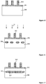
- FIG. 17 As shown in Figure 17 , at the beginning of the fabrication process, a semiconductor substrate with certain structures is provided (S301). Figure 10 illustrates a corresponding semiconductor structure.
- a semiconductor substrate 300 may be provided; and a hard mask layer 302 may be formed on the semiconductor substrate 300.
- the position of the hard mask layer 302 may correspond to the position of subsequently formed fin. Details of the hard mask layer 302 can be referred to the above descriptions associated with Figure 16 and are not repeated here.
- FIG. 11 illustrates a corresponding semiconductor structure.
- an anti-punch-through ion implantation process 31 may be performed to form a doping region 304 in the semiconductor substrate 300.
- the hard mask layer 302 may prevent the semiconductor substrate 300 under the hard mask layer 302 (position for subsequently forming the fin) from being susceptible to ion implantation damages. That is, the subsequently formed fin in the semiconductor substrate 300 under the hard mask layer 302 may be susceptible to less ion implantation damages. Further, the hard mask layer 302 may precisely define the position of the doping region 304 formed in the semiconductor substrate 300. Thus, when a subsequent annealing process is performed, impurity ions in the doping region 304 may diffuse into the semiconductor substrate 300 under the hard mask layer 302 to form an anti-punch-through region. The position of the anti-punch-through region may be relatively accurate, and concentration of impurity ions in the anti-punch-through region may meet the fabrication process requirements.
- the impurity ions implanted by the anti-punch-through ion implantation process 31 may be N-type impurity ions or P-type impurity ions.
- the formed FinFET may be an N-type FinFET and the type of impurity ions implanted by the anti-punch-through ion implantation process may be P-type.
- the P-type impurity ion may include one or more of boron ions, gallium ions, and indium ions.
- the formed FinFET may be a P-type FinFET and the type of impurity ions implanted by the anti-punch-through ion implantation process may be N-type.
- the N-type impurity ion may include one or more of phosphorus ions, arsenic ions, and antimony ions.
- the implantation angle of the anti-punch-through ion implantation process 31 may be in a range of approximately 0-10 degrees; the implantation energy may be in a range of approximately 3-10 KeV; and the dose may be in a range of approximately 1 ⁇ 10 14 - 1 ⁇ 10 20 atoms/cm 3 .
- an annealing process is performed to form an anti-punch-through region (S303).
- Figure 12 illustrates a corresponding semiconductor structure.
- an annealing process may be performed onto the doping region 304, where impurity ions in the doping region 304 may diffuse into the semiconductor substrate 300 under the hard mask layer 302 to form an anti-punch-through region 307.
- the annealing temperature may be in a range of approximately 900-1300 °C; and the annealing time may be in a range of approximately 30 seconds-10 minutes.
- FIG. 13 illustrates a corresponding semiconductor structure.
- the hard mask layer 302 may be used as a mask to etch the semiconductor substrate 300 and the doping region 304 (referring to Figure 12 ) to form a trench 311.
- the semiconductor substrate between the adjacent trenches 311 may include a fin 309.
- FIG. 14 illustrates a corresponding semiconductor structure.
- a shallow trench isolation structure 313 may be formed in the trench 311.
- the surface of the shallow trench isolation structure 311 may be below the top surface of the fin 309.
- FIG. 15 illustrates a corresponding semiconductor structure.
- the hard mask layer may be removed.
- a gate structure crossing and covering the top and side surfaces of the fin may be formed.
- the gate structure may include a gate dielectric layer 314 on the top and side surfaces of the fin 309 and a gate electrode 315 on the gate dielectric layer 314. Further, source and drain regions may be formed in the fins 309 at both sides of the gate structure.
Landscapes
- Insulated Gate Type Field-Effect Transistor (AREA)
- Metal-Oxide And Bipolar Metal-Oxide Semiconductor Integrated Circuits (AREA)
- Chemical & Material Sciences (AREA)
- Crystallography & Structural Chemistry (AREA)
Abstract
Description
- This application claims the priority of Chinese patent application No.
201511025328.X, filed on December 30,2015 - The present invention generally relates to the field of semiconductor manufacturing technology and, more particularly, relates to a FinFET and fabrication techniques thereof.
- With the continuous development of semiconductor process technology, process node is gradually reduced and gate-last process has been widely used, to achieve the desired threshold voltage and to improve the performance of device. However, when the critical dimensions of the device further decline, even with the gate-last process, the structure of conventional metal-oxide-semiconductor (MOS) field-effect transistor (FET) has been unable to meet the demand for the device performance, therefore a FinFET as an alternative to a conventional device has been widely concerned.
- Referring to
Figure 1 , a FinFET fabricated with existing techniques includes: asemiconductor substrate 200 having aprotruding fin 201 formed on thesemiconductor substrate 200; anisolation layer 205 covering the surface of thesemiconductor substrate 200 and part of side walls of thefin 201; agate structure 203 crossing the fin and covering part of top and side surfaces of thefin 201, and thegate structure 203 includes a gate dielectric layer and a gate electrode on the gate dielectric layer;sidewall spacers 204 formed on both side walls of thegate structure 203; a source region and a drain region formed in thefin 201 at both sides of thegate structure 203 and thesidewall spacers 204. - For such FinFET, the contacting region between the top and both side walls of the
fin 201 and thegate structure 203 is a channel region, which is desired to increase the drive current and to improve the performance of the device. - However, in such FinFET fabricated with existing techniques, a source-drain punch-through phenomenon easily appears between the source region and the drain region and affects the performance of the FinFET. The disclosed device structures and methods are directed to solve one or more problems set forth above and other problems.
- A first aspect of the present invention includes a method for fabricating a FinFET. The method includes providing a semiconductor substrate and forming a hard mask layer on the semiconductor substrate, wherein a position of the hard mask layer may corresponds to a position of subsequently formed fin. The method also includes forming a doping region in the semiconductor substrate by using the hard mask layer as a mask to perform an anti-punch-through ion implantation process. Further, the method includes forming an anti-punch-through region by performing an annealing process onto the doping region, such that impurity ions in the doping region diffuse into the semiconductor substrate under the hard mask layer. Furthermore, the method includes forming a trench by using the hard mask layer as a mask to etch the semiconductor substrate and the doping region, wherein the semiconductor substrates between the adjacent trenches constitutes a fin.
- Preferably, an implantation angle of the anti-punch-through ion implantation process is in a range of approximately 0-10 degrees.
- Preferably, an implantation energy of the anti-punch-through ion implantation process is in a range of approximately 3-10 KeV.
- Preferably, a dose of the anti-punch-through ion implantation process is in a range of approximately 1×10¹⁴-1×10²⁰ atoms/cm3.
- Preferably, an annealing temperature is in a range of approximately 900-1300 °C.
- Preferably, an annealing time is in a range of approximately 30 seconds-10 minutes.
- Preferably, a width of the hard mask layer is in a range of approximately 10-50 nm.
- The impurity ions implanted by the anti-punch-through ion implantation process may be N-type impurity ions, or P-type impurity ions.
- In one embodiment, the formed FinFET is an N-type FinFET, and the impurity ions implanted by the anti-punch-through ion implantation process are P-type impurity ions.
- In an alternative embodiment, the formed FinFET is a P-type FinFET, and the impurity ions implanted by the anti-punch-through ion implantation process are N-type impurity ions.
- Preferably, the method comprises forming a shallow trench isolation structure, wherein a surface of the shallow trench isolation structure is below a top surface of the fin; removing the hard mask layer; forming a gate structure crossing and covering top and side surfaces of the fin; and forming source and drain regions in the fins at both sides of the gate structure.
- A second aspect of the present invention includes a further development of the method for fabricating a FinFET. The further development of the method includes providing the semiconductor substrate having a first region and a second region and forming the hard mask layer on the semiconductor substrate in the first region and the second region, wherein a position of the hard mask layer on the semiconductor substrate in the first region corresponds to a position of the subsequently formed fin as a first fin, and a position of the hard mask layer on the semiconductor substrate in the second region corresponds to a position of subsequently formed second fin. The method also includes forming the doping region being a first doping region in the semiconductor substrate in the first region by using the hard mask layer on the semiconductor substrate in the first region as a mask to perform the anti-punch-through ion implantation process as a first anti-punch-through ion implantation process. In addition, the method includes forming a second doping region in the semiconductor substrate in the second region by using the hard mask layer on the semiconductor substrate in the second region as a mask to perform a second anti-punch-through ion implantation process, wherein a type of impurity ions implanted by the second anti-punch-through ion implantation process is different from the type of impurity ions implanted by the first anti-punch-through ion implantation process. Moreover, the method includes performing the annealing process onto the first doping region and the second doping region, wherein the impurity ions in the first doping region diffuse into the semiconductor substrate in the first region under the hard mask layer to form the anti-punch-through region as a first anti-punch-through region, and the impurity ions in the second doping region diffuse into the semiconductor substrate in the second region under the hard mask layer to form a second anti-punch-through region. Further, the method includes forming the trenches as first trenches by using the hard mask layer on the semiconductor substrate in the first region as the mask to etch the semiconductor substrate in the first region and the first doping region, wherein the semiconductor substrate between the adjacent first trenches constitutes the fin as a first fin. Furthermore, the method includes forming second trenches by using the hard mask layer on the semiconductor substrate in the second region as a mask to etch the semiconductor substrate in the second region and the second doping region, wherein the semiconductor substrate between the adjacent second trenches constitutes a second fin.
- In one embodiment, a P-type FinFET is formed in the semiconductor substrate in the first region, and the type of the impurity ions implanted by the first anti-punch-through ion implantation process is N-type, and an N-type FinFET is formed in the semiconductor substrate in the second region, and the type of impurity ions implanted by the second anti-punch-through ion implantation process is P-type.
- In an alternative embodiment, an N-type FinFET is formed in the semiconductor substrate in the first region and the type of the impurity ions implanted by the first anti-punch-through ion implantation process is P-type, and a P-type FinFET is formed in the semiconductor substrate in the second region and the type of impurity ions implanted by the second anti-punch-through ion implantation process is N-type.
- Preferably, an implantation angle of the first anti-punch-through ion implantation process is in a range of approximately 0-10 degrees.
- Preferably, an implantation energy of the first anti-punch-through ion implantation process is in a range of approximately 3-10 KeV.
- Preferably, a dose of the first anti-punch-through ion implantation process is in a range of approximately 1×10¹⁴-1×10²⁰ atoms/cm3.
- Preferably, an implantation angle of the second anti-punch-through ion implantation process is in a range of approximately 0-10 degrees.
- Preferably, an implantation energy of the second anti-punch-through ion implantation process is in a range of approximately 3-10 KeV.
- Preferably, a dose of the second anti-punch-through ion implantation process is in a range of approximately 1×10¹⁴-1×10²⁰ atoms/cm3.
- Preferably, an annealing temperature is in a range of approximately 900-1300 °C, and an annealing time is in a range of approximately 30 seconds-10 minutes.
- Preferably, a width of the hard mask layer is in a range of approximately 10-50 nm.
- The method may further include: forming a shallow trench isolation structure in the first trench and the second trench, wherein a surface of the shallow trench isolation structure is below top surfaces of the first fin and the second fin; removing the hard mask layer; forming a first gate structure crossing and covering top and side surfaces of the first fin; forming first source and drain regions in the fins at both sides of the first gate structure; forming a second gate structure crossing and covering top and side surfaces of the second fin; and forming second source and drain regions in the fins at both sides of the second gate structure.
- Other aspects of the present invention can be understood by those skilled in the art in light of the description, the claims, and the drawings of the present invention.
-
-
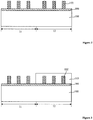
Figure 1 illustrates a FinFET structure corresponding to an existing fabrication process of a FinFET; -
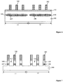
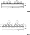
Figures 2-9 illustrate FinFET structures corresponding to certain stages of a fabrication process of a FinFET consistent with the disclosed embodiments; -
Figures 10-15 illustrate FinFET structures corresponding to certain stages of another fabrication process of a FinFET consistent with the disclosed embodiments; -
Figure 16 illustrates an exemplary FinFET fabrication process consistent with the disclosed embodiments; and -
Figure 17 illustrates another exemplary FinFET fabrication process consistent with the disclosed embodiments. - As explained in the background section, in a FinFET fabricated with existing techniques, a source-drain punch-through phenomenon easily appears between the source region and the drain region and affects the performance of the FinFET.
- Referring to
Figure 1 , in order to form a channel region in afin 201 covered by agate structure 203, the distance between the bottom of source and drain regions in thefin 201 and the top of thefin 201 may be large, such that the channel region formed at both side walls of thefin 201 can also be driven by the source and drain regions. However, when the distance between the bottom of the source and drain regions and the top of thefin 201 is large, the control ability of thegate structure 203 at the top of thefin 201 to the bottom of the source and drain regions may be low. Therefore, a punch-through phenomenon appears at the bottom of the source and drain regions and the performance of formed FinFET is degraded. - To prevent the source-drain punch-through phenomenon, one method is to form an anti-punch-through layer at the bottom of the
fin 201. Specifically, after forming thefin 201 on thesemiconductor substrate 200 and before forming theisolation layer 205, the anti-punch-through layer may be formed at the bottom of thefin 201 by an ion implantation process. The type of doped impurity ions in the anti-punch-through layer is in opposite to the type of doped impurity ions in the source and drain regions to avoid the occurrence of the punch-through phenomenon at the bottom of the source and drain regions. However, the ion implantation process for forming the anti-punch-through layer may cause implantation damages on the surface of thefin 201, leading to poor surface morphology of thefin 201. Therefore, the performance of the FinFET formed in thefin 201 may still be degraded. - Reference will now be made in detail to exemplify embodiments of the invention, which are illustrated in the accompanying drawings. Wherever possible, the same reference numbers will be used throughout the drawings to refer to the same or like parts.
-
Figure 16 illustrates an exemplary FinFET fabrication process consistent with the disclosed embodiments.Figures 2-9 illustrate FinFET structures corresponding to certain stages of the exemplary fabrication process. - As shown in
Figure 16 , at the beginning of the fabrication process, a semiconductor substrate with certain structures is provided (S201).Figure 2 illustrates a corresponding semiconductor structure. - Referring to
Figure 2 , asemiconductor substrate 100 is provided, and thesemiconductor substrate 100 may have afirst region 11 and asecond region 12. Further, ahard mask layer 102 may be formed on thesemiconductor substrate 100 in thefirst region 11 and in thesecond region 12. The position of thehard mask layer 102 on the semiconductor substrate in thefirst region 11 may correspond to the position of subsequently formed first fin, and the position of thehard mask layer 102 on the semiconductor substrate in thesecond region 12 may corresponds to the position of subsequently formed second fin. - The
semiconductor substrate 100 may include any appropriate semiconductor material, such as one or more of silicon (Si), germanium (Ge), germanium-silicon alloy (GeSi), silicon carbide (SiC), silicon on insulator (SOI), germanium on insulator (GOI), gallium arsenide (GaAs), and other III-V compounds. - The
semiconductor substrate 100 may have afirst region 11 and asecond region 12, where thefirst region 11 and thesecond region 12 may be adjacent or nonadjacent to each other. In one embodiment, the adjacentfirst region 11 andsecond region 12 are used as an example to illustrate. Different types of FinFETs may be separately formed on the semiconductor substrate in thefirst region 11 and on the semiconductor substrate in thesecond region 12. In one embodiment, an N-type FinFET is formed on the semiconductor substrate in thefirst region 11 and a P-type FinFET is formed on the semiconductor substrate in thesecond region 12. In certain other embodiments, a P-type FinFET is formed on the semiconductor substrate in thefirst region 11 and an N-type FinFET is formed on the semiconductor substrate in thesecond region 12. - As shown in
Figure 2 , ahard mask layer 102 may be formed on thesemiconductor substrate 100 in thefirst region 11 and thesecond region 12. Thehard mask layer 102 on the semiconductor substrate in thefirst region 11 is used as a mask to subsequently etch the semiconductor substrate to form a first fin. The position and width of thehard mask layer 102 on the semiconductor substrate in thefirst region 11 are corresponding to the position and width of the subsequently formed first fin. - Further, the
hard mask layer 102 on the semiconductor substrate in thefirst region 11 may also be used as a mask layer and a protective layer for a first anti-punch-through ion implantation process. As the mask layer, thehard mask layer 102 on the semiconductor substrate in thefirst region 11 defines the position of a first doping region in the semiconductor substrate in thefirst region 11. As the protective layer, thehard mask layer 102 on the semiconductor substrate in thefirst region 11 can prevent the implantation damages of the first anti-punch-through ion implantation process onto the semiconductor substrate under thehard mask layer 102. Thus, the surface of the subsequently formed first fin by etching the semiconductor substrate in thefirst region 11 can avoid implantation damages. - Similarly, the
hard mask layer 102 on the semiconductor substrate in thesecond region 12 is used as a mask to subsequently etch the semiconductor substrate to form a second fin. The position and width of thehard mask layer 102 on the semiconductor substrate in thesecond region 12 are corresponding to the position and width of the subsequently formed second fin. - Further, the
hard mask layer 102 on the semiconductor substrate in thesecond region 12 may also be used as a mask layer and a protective layer for a second anti-punch-through ion implantation process. As the mask layer, thehard mask layer 102 on the semiconductor substrate in thesecond region 12 defines the position of a second doping region in the semiconductor substrate in thesecond region 12. As the protective layer, thehard mask layer 102 on the semiconductor substrate in thesecond region 12 can prevent the implantation damages of the second anti-punch-through ion implantation process onto the semiconductor substrate under thehard mask layer 102. Thus, the surface of the subsequently formed second fin by etching the semiconductor substrate in thesecond region 12 can avoid the implantation damages. - The number of layers of the hard mask layer on the semiconductor substrate in the
first region 11 is at least one; and the number of layers of the hard mask layer on the semiconductor substrate in thesecond region 12 is at least one. - The
hard mask layer 102 may be made of SiO2, SiN, SiON, SiCN, SiC, BN, TiN, and/or TaN. Thehard mask layer 102 may have a single layer or multilayer (≧ 2 layers) stacked structure. In one embodiment, thehard mask layer 102 may be a two-layer stacked structure, including a first mask layer and a second mask layer formed on the first mask layer. The first mask layer and the second mask layer may be made of different materials. The first mask layers may be made of SiO2, SiN, SiON, SiCN, SiC, and/or BN; and the second mask layers may be made of SiO2, SiN, SiON, SiCN, SiC, BN, TiN, and/or TaN. - The fabrication process of the
hard mask layer 102 includes: forming a hard mask thin film layer on thesemiconductor substrate 100; forming a patterned photoresist layer on the hard mask thin film layer; and using the patterned photoresist layer as a mask to etch the hard mask thin film layer to form thehard mask layer 102 on the semiconductor substrate in thefirst region 11 and thesecond region 12. In one embodiment, thehard mask layer 102 may be fabricated by a double patterning process. - The width of the hard mask layer may not be too wide. If the width of the hard mask layer is too wide, during a subsequent annealing process, it may be difficult for a process to form a first anti-punch-through region and a second anti-punch-through region by diffusion of impurity ions in the first doping region and the second doping region. The width of the hard mask layer may not be too small. If the width of the hard mask layer is too small, it may be difficult for a process to form a first fin and a second fin by an etching process. In one embodiment, the width of the hard mask layer may be in a range of approximately 10-50 nm, such as 10 nm, 15 nm, 20 nm, 30 nm, 40 nm, 45 nm, and 50 nm.
- In one embodiment, before forming the
hard mask layer 102, aprotective layer 101 may be formed on the semiconductor substrate. Theprotective layer 101 can be used as a grinding stop layer for subsequently forming a shallow trench isolation structure. After forming theprotective layer 101, the hard mask layer may be correspondingly formed on theprotective layer 101. - Returning to
Figure 16 , after forming the hard mark layer on the semiconductor substrate, a photoresist layer is formed (S202).Figure 3 illustrates a corresponding semiconductor structure. - As shown in
Figure 3 , aphotoresist layer 103 may be formed, covering thehard mask layer 102 on the semiconductor substrate in thesecond region 12 and thesemiconductor substrate 100 in thesecond region 12. - The
photoresist layer 103 may protect the semiconductor substrate in thesecond region 12 from being injected with impurity ions when a subsequent first anti-punch-through ion implantation process is performed. - In one embodiment, the fabrication process of the
photoresist layer 103 may be a spin coating process, and the photoresist layer on the semiconductor substrate in thefirst region 11 may then be removed by exposure and development processes. - Returning to
Figure 16 , after forming the photoresist layer, a first doping region is formed (S203).Figure 4 illustrates a corresponding semiconductor structure. - As shown in
Figure 4 , thehard mask layer 102 on the semiconductor substrate in thefirst region 11 may be used as a mask to perform a first anti-punch-throughion implantation process 21 to form afirst doping region 104 in the semiconductor substrate in thefirst region 11. - When the first anti-punch-through
ion implantation process 21 is performed, thehard mask layer 102, on the semiconductor substrate in thefirst region 11, may prevent the semiconductor substrate100 under the hard mask layer 102 (the position for subsequently forming a first fin) from being subject to ion implantation damages. That is, the subsequently formed first fin in the semiconductor substrate in thefirst region 11 under thehard mask layer 102 may be less susceptible to ion implantation damages. - Further, the
hard mask layer 102 on the semiconductor substrate in thefirst region 11 may precisely define the position of thefirst doping region 104 formed in thesemiconductor substrate 100. Therefore, when a subsequent annealing process is performed, the impurity ions in thefirst doping region 104 diffuse into thesemiconductor substrate 100 in thefirst region 11 under thehard mask layer 102 to form a first anti-punch-through region. The position of the first anti-punch-through region is relatively accurate, and concentration of impurity ions in the first anti-punch-through region meets the fabrication process requirements. - In one embodiment, an N-type FinFET may be formed in the
semiconductor substrate 100 in thefirst region 11 and the type of impurity ions implanted by the first anti-punch-throughion implantation process 21 may be P-type. The P-type impurity ions may include one or more of boron ions, gallium ions, and indium ions. - In certain other embodiments, a P-type FinFET is formed in the
semiconductor substrate 100 in thefirst region 11 and the type of impurity ions implanted by the first anti-punch-throughion implantation process 21 may be N-type. The N-type impurity ion may include one or more of phosphorus ions, arsenic ions, and antimony ions. - In one embodiment, the implantation angle of the first anti-punch-through
ion implantation process 21 may be in a range of approximately 0-10 degrees; the implantation energy of the first anti-punch-throughion implantation process 21 may be in a range of approximately 3-10 KeV; and the dose of the first anti-punch-throughion implantation process 21 may be in a range of approximately 1×10¹⁴-1×10²⁰ atoms/cm3. - Returning to
Figure 16 , after forming the first doping region, a second doping region is formed (S204).Figure 5 illustrates a corresponding semiconductor structure. - As shown in
Figure 5 , thehard mask layer 102 on the semiconductor substrate in thesecond region 12 may be used as a mask to perform a second anti-punch-throughion implantation process 22 to form asecond doping region 106 in thesemiconductor substrate 100 in thesecond region 12. The type of impurity ions implanted by the second anti-punch-throughion implantation process 22 may be different from the type of impurity ions implanted by the first anti-punch-throughion implantation process 21. - Before performing the second anti-punch-through
ion implantation process 22, thephotoresist layer 103 on the semiconductor substrate in the second region 12 (referring toFigure 4 ) may be removed and aphotoresist layer 105 may be formed to cover thehard mask layer 102 on thesemiconductor substrate 100 in thefirst region 11 and thesemiconductor substrate 100 in thefirst region 11. - In one embodiment, an N-type FinFET may be formed in the
semiconductor substrate 100 in thefirst region 11 and the type of impurity ions implanted by the first anti-punch-throughion implantation process 21 may be P-type. A P-type FinFET may be formed in thesemiconductor substrate 100 in thesecond region 12 and the type of impurity ions implanted by the second anti-punch-throughion implantation process 22 may be N-type. The N-type impurity ion may include one or more of phosphorus ions, arsenic ions, and antimony ions. - In certain other embodiments, a P-type FinFET may be formed in the
semiconductor substrate 100 in thefirst region 11 and the type of impurity ions implanted by the first anti-punch-throughion implantation process 21 may be N-type. An N-type FinFET may be formed in thesemiconductor substrate 100 in thesecond region 12 and the type of impurity ions implanted by the second anti-punch-throughion implantation process 22 may be P-type. The P-type impurity ion may include one or more of boron ions, gallium ions, and indium ions. - When the second anti-punch-through
ion implantation process 22 is performed, thehard mask layer 102 on the semiconductor substrate in thesecond region 12 may prevent the semiconductor substrate100 under the hard mask layer 102 (the position for subsequently forming the second fin) from being susceptible to ion implantation damages. That is, the subsequently formed second fin in thesemiconductor substrate 100 in thesecond region 12 under thehard mask layer 102 may be less susceptible to ion implantation damages. Further, thehard mask layer 102 on the semiconductor substrate in thesecond region 12 may precisely define the position of thesecond doping region 106 formed in thesemiconductor substrate 100. Therefore, when a subsequent annealing process is performed, impurity ions in thesecond doping region 106 may diffuse into thesemiconductor substrate 100 in thesecond region 12 under thehard mask layer 102 to form a second anti-punch-through region. The position of the second anti-punch-through region may be relatively accurate, and concentration of impurity ions in the second anti-punch-through region may meet the fabrication process requirements. - In one embodiment, the implantation angle of the second anti-punch-through
ion implantation process 22 may be in a range of approximately 0-10 degrees; the implantation energy of the second anti-punch-throughion implantation process 22 may be in a range of approximately 3-10 KeV; and the dose of the second anti-punch-throughion implantation process 22 maybe in a range of approximately 1×10¹⁴-1×10²⁰ atoms/cm3. - Returning to
Figure 16 , after forming the second doping region, a first anti-punch-through region and a second anti-punch-through region are formed (S205).Figure 6 illustrates a corresponding semiconductor structure. - As shown in
Figure 6 , an annealing process may be performed onto thefirst doping region 104 and thesecond doping region 106. Therefore, impurity ions in thefirst doping region 104 may diffuse into thesemiconductor substrate 100 in thefirst region 11 under thehard mask layer 102 to form a first anti-punch-throughregion 107. Also, impurity ions in thesecond doping region 106 may diffuse into thesemiconductor substrate 100 in thesecond region 12 under thehard mask layer 102 to form a second anti-punch-throughregion 108. - The width of the
hard mask layer 102 may be in a range of approximately 10-50 nm. Accordingly, the width of subsequently formed first fin and second fin may also be in a range of approximately 10-50 nm, and the diffusion width of impurity ions in thefirst doping region 104 and thesecond doping region 106 may be in a range of approximately 10-50 nm. In one embodiment, the annealing temperature may be in a range of approximately 900-1300 °C, and the annealing time may be in a range of approximately 30 seconds-10minutes, such that the impurity ions in thefirst doping region 104 and thesecond doping region 106 may sufficiently diffuse into the semiconductor substrate under thehard mask layer 102. - To better illustrate the distinction between the doping region and the anti-punch-through region in
Figure 6 , the dashed boxes may be used to indicate the first anti-punch-throughregion 107 and the second anti-punch-throughregion 108. - Returning to
Figure 16 , after forming the first anti-punch-through region and the second anti-punch-through region, a first trench and a second trench are formed (S206).Figure 7 illustrates a corresponding semiconductor structure. - As shown in
Figure 7 , after performing an annealing process, thehard mask layer 102 on the semiconductor substrate in thefirst region 11 may be used as a mask to etch thesemiconductor substrate 100 in thefirst region 11 and the first doping region 104 (referring toFigure 6 ) to form afirst trench 111. The semiconductor substrate between the adjacentfirst trenches 111 may include afirst fin 109. Further, thehard mask layer 102 on the semiconductor substrate in thesecond region 12 may be used as a mask to etch thesemiconductor substrate 100 in thesecond region 12 and the second doping region 106 (referring toFigure 6 ) to form asecond trench 112. The semiconductor substrate between the adjacentsecond trenches 112 constitutes asecond fin 110. - The depth of the formed
first trench 111 may be greater than the depth of thefirst doping region 104, such that the formed adjacentfirst fins 109 may not be electrically connected by the first anti-punch-throughregion 107. Similarly, the depth of the formedsecond trench 112 may be greater than the depth of thesecond doping region 106, such that the formed adjacentsecond fins 110 may not be electrically connected by the second anti-punch-throughregion 108. - An anisotropic dry etching process may be performed to etch the
semiconductor substrate 100. In one embodiment, the anisotropic dry etching process may be a plasma etching process. Etching gases used in the plasma etching process may include CF4, HBr, He and O2. The flow rate of CF4 gas may be in a range of approximately 20-200 sccm; the flow rate of HBr gas may be in a range of approximately 80-900 sccm; the flow rate of He gas may be in a range of approximately 250-950 sccm; the flow rate of O2 gas may be in a range of approximately 5-20 sccm; the chamber pressure may be in a range of approximately 10-80 mTorr; the chamber temperature may be in a range of approximately 20-100 °C; the RF power may be in a range of approximately 200-2000 W; and the RF bias power may be in a range of approximately 0-150 W. - Returning to
Figure 16 , after forming the first trench and the second trench, a shallow trench isolation structure is formed and the hard mask layer is removed (S207).Figure 8 illustrates a corresponding semiconductor structure. - As shown in
Figure 8 , a shallowtrench isolation structure 113 may be formed in thefirst trench 111 and thesecond trench 112. The surface of the shallowtrench isolation structure 113 may be below the top surfaces of thefirst fin 109 and thesecond fin 110. Further, thehard mask layer 102 may be removed (referring toFigure 7 ). - The shallow
trench isolation structure 113 may be configured to isolate the adjacentfirst fins 109 and to isolate the adjacentsecond fins 110. - The fabrication process of the shallow
trench isolation structure 113 may include: forming an isolation material layer covering thesemiconductor substrate 100, thefirst fin 109 and thesecond fin 110; planarizing the insulation material layer until the top surfaces of thefirst fin 109 and thesecond fin 110 are exposed, where a planarization process may include a chemical mechanical polishing process; and removing part of thickness of the planarized insulation material layer by a back etching process to form the shallowtrench isolation structure 113 in thefirst trench 111 and thesecond trench 112. The surface of the shallowtrench isolation structure 113 may be below the top surfaces of thefirst fin 109 and thesecond fin 110. - When planarizing the insulation material layer, the protective layer and the hard mask layer on top surfaces of the
first fin 109 and thesecond fin 110 may be removed by the planarization process. The shallowtrench isolation structure 113 may be made of any appropriate material, such as SiO2, SiON, SiOCN, and/or SiOBN. - In one embodiment, the surface of the shallow
trench isolation structure 113 may level with the surfaces of the first anti-punch-through region and the second anti-punch-through region. The surface of the shallowtrench isolation structure 113 may also be slightly above or slightly below the surfaces of the first anti-punch-through region and the second anti-punch-through region. - Returning to
Figure 16 , after forming the shallow trench isolation structure, a first gate structure, first source and drain regions, a second gate structure, and second source and drain regions are formed (S208).Figure 9 illustrates a corresponding semiconductor structure. - As shown in
Figure 9 , afirst gate structure 118 crossing and covering the top and side surfaces of thefirst fin 109 may be formed, and first source and drain regions may be formed in the fins at both sides of the first gate structure 118 (not labeled). Further, asecond gate structure 119 crossing and covering the top and side surfaces of thesecond fin 110 may be formed; and second source and drain regions may be formed in the fins at both sides of the second gate structure 119 (not labeled).Figure 9 and foregoing figures may show cross-sectional views along an x-axis direction inFigure 1 . - The
first gate structure 118 may include a fistgate dielectric layer 114 on the top and side surfaces of thefirst fin 109, and afirst gate electrode 115 on the firstgate dielectric layer 114. - The
second gate structure 119 may include a secondgate dielectric layer 116 on the top and side surfaces of thesecond fin 110, and asecond gate electrode 117 on the secondgate dielectric layer 116. - In one embodiment, the first
gate dielectric layer 114 and/or the secondgate dielectric layer 116 may be made of silicon oxide. Thefirst gate electrode 115 and/or thesecond gate electrode 117 may be made of polysilicon. - In certain other embodiments, the first
gate dielectric layer 114 and/or the secondgate dielectric layer 116 may be made of any appropriate high-K dielectric material, such as one or more of HfO2, Al2O3, ZrO2, HfSiO, HfSiON, HfTaO, and HfZrO. Thefirst gate electrode 115 and/or thesecond gate electrode 117 may be made of metal, such as one or more of W, Al, Cu, and Ti. - The
first gate structure 118 may cross and cover the top and side surfaces of one or more (≥ 2) of thefirst fins 109. Thesecond gate structure 119 may cross and cover the top and side surfaces of one or more (≥ 2) of thesecond fins 110. - After forming the
first gate structure 118, first side wall spacers may be formed at both side surfaces of thefirst gate structure 118. Using thefirst gate structure 118 and the first side wall spacers as a mask, an ion implantation process may be performed onto the first fins at both sides of thefirst gate structure 118 and the first side wall spacers to form first source and drain regions in the first fins at both sides of thefirst gate structure 118 and the first side wall spacers. - In one embodiment, the
first gate structure 118 and the first side wall spacers may be used as a mask to etch the first fins at both sides of thefirst gate structure 118 and the first side wall spacers to form a trench. The trench may be filled with a stress layer to form first source and drain regions that are strained. The stress layer may cause stress to the channel region and improve the carrier mobility in the channel region. The stress layer may be made of any appropriate material, such as germanium silicon, and/or silicon carbide. - The depth of the first source and drain regions may be the same as the depth of the first anti-punch-through
region 107. The depth of the first source and drain regions may also be slightly smaller than the depth of the first anti-punch-throughregion 107, such that the first anti-punch-throughregion 107 may have a desired anti-punch-through effect to the first source and drain regions. - After forming the
second gate structure 119, second side wall spacers may be formed at both side surfaces of thesecond gate structure 119. Using thesecond gate structure 119 and the second side wall spacers as a mask, an ion implantation process may be performed onto the second fins at both sides of thesecond gate structure 119 and the second side wall spacers to form second source and drain regions in the second fins at both sides of thesecond gate structure 119 and the second side wall spacers. - In one embodiment, the
second gate structure 119 and the second side wall spacers may be used as a mask to etch the second fins at both sides of thesecond gate structure 119 and the second side wall spacers to form a trench. The trench may be filled with a stress layer to form second source and drain regions that are strained. The stress layer may cause stress to the channel region and improve the carrier mobility in the channel region. The stress layer may be made of any appropriate material, such as germanium silicon and/or silicon carbide. - The depth of the second source and drain regions may be the same as the depth of the second anti-punch-through
region 108. The depth of the second source and drain regions may also be slightly smaller than the depth of the second anti-punch-throughregion 108, such that the second anti-punch-throughregion 108 may have a desired anti-punch-through effect to the second source and drain regions. -
Figure 17 illustrates another exemplary FinFET fabrication process consistent with the disclosed embodiments.Figures 10-15 illustrate another FinFET structure corresponding to certain stages of the exemplary fabrication process. - The difference between the fabrication process illustrated in
Figure 17 and the fabrication process illustrated inFigure 16 may be that the FinFET formed through the fabrication process shown inFigure 17 may include one type (one of N-type and P-type) of FinFET, and the FinFET formed through the fabrication process shown inFigure 16 may include two types (N-type and P-type) of FinFET formed simultaneously. - As shown in
Figure 17 , at the beginning of the fabrication process, a semiconductor substrate with certain structures is provided (S301).Figure 10 illustrates a corresponding semiconductor structure. - Referring to
Figure 10 , asemiconductor substrate 300 may be provided; and ahard mask layer 302 may be formed on thesemiconductor substrate 300. The position of thehard mask layer 302 may correspond to the position of subsequently formed fin. Details of thehard mask layer 302 can be referred to the above descriptions associated withFigure 16 and are not repeated here. - Returning to
Figure 17 , after forming the hard mark layer on the semiconductor substrate, a doping region is formed (S302).Figure 11 illustrates a corresponding semiconductor structure. - As shown in
Figure 11 , using thehard mask layer 302 as a mask, an anti-punch-throughion implantation process 31 may be performed to form adoping region 304 in thesemiconductor substrate 300. - When the anti-punch-through
ion implantation process 31 is performed, thehard mask layer 302 may prevent thesemiconductor substrate 300 under the hard mask layer 302 (position for subsequently forming the fin) from being susceptible to ion implantation damages. That is, the subsequently formed fin in thesemiconductor substrate 300 under thehard mask layer 302 may be susceptible to less ion implantation damages. Further, thehard mask layer 302 may precisely define the position of thedoping region 304 formed in thesemiconductor substrate 300. Thus, when a subsequent annealing process is performed, impurity ions in thedoping region 304 may diffuse into thesemiconductor substrate 300 under thehard mask layer 302 to form an anti-punch-through region. The position of the anti-punch-through region may be relatively accurate, and concentration of impurity ions in the anti-punch-through region may meet the fabrication process requirements. - The impurity ions implanted by the anti-punch-through
ion implantation process 31 may be N-type impurity ions or P-type impurity ions. - In one embodiment, the formed FinFET may be an N-type FinFET and the type of impurity ions implanted by the anti-punch-through ion implantation process may be P-type. The P-type impurity ion may include one or more of boron ions, gallium ions, and indium ions.
- In certain other embodiments, the formed FinFET may be a P-type FinFET and the type of impurity ions implanted by the anti-punch-through ion implantation process may be N-type. The N-type impurity ion may include one or more of phosphorus ions, arsenic ions, and antimony ions.
- In one embodiment, the implantation angle of the anti-punch-through
ion implantation process 31 may be in a range of approximately 0-10 degrees; the implantation energy may be in a range of approximately 3-10 KeV; and the dose may be in a range of approximately 1×10¹⁴- 1×10²⁰ atoms/cm3. - Returning to
Figure 17 , after forming the doping region, an annealing process is performed to form an anti-punch-through region (S303).Figure 12 illustrates a corresponding semiconductor structure. - As shown in
Figure 12 , an annealing process may be performed onto thedoping region 304, where impurity ions in thedoping region 304 may diffuse into thesemiconductor substrate 300 under thehard mask layer 302 to form an anti-punch-throughregion 307. - In one embodiment, the annealing temperature may be in a range of approximately 900-1300 °C; and the annealing time may be in a range of approximately 30 seconds-10 minutes.
- Returning to
Figure 17 , after forming the anti-punch-through region, an etching process is performed to form a trench (S304).Figure 13 illustrates a corresponding semiconductor structure. - As shown in
Figure 13 , after performing the annealing process, thehard mask layer 302 may be used as a mask to etch thesemiconductor substrate 300 and the doping region 304 (referring toFigure 12 ) to form atrench 311. The semiconductor substrate between theadjacent trenches 311 may include afin 309. - Returning to
Figure 17 , after forming the trench, a shallow trench isolation structure is formed (S305).Figure 14 illustrates a corresponding semiconductor structure. - As shown in
Figure 14 , a shallowtrench isolation structure 313 may be formed in thetrench 311. The surface of the shallowtrench isolation structure 311 may be below the top surface of thefin 309. - Returning to
Figure 17 , after forming the shallow trench isolation structure, a gate structure, and source and drain regions are formed (S306).Figure 15 illustrates a corresponding semiconductor structure. - As shown in
Figure 15 , the hard mask layer may be removed. A gate structure crossing and covering the top and side surfaces of the fin may be formed. The gate structure may include a gate dielectric layer 314 on the top and side surfaces of thefin 309 and a gate electrode 315 on the gate dielectric layer 314. Further, source and drain regions may be formed in thefins 309 at both sides of the gate structure.
Claims (15)
- A method for fabricating a fin field-effect transistor, FinFET, comprising:providing a semiconductor substrate;forming a hard mask layer on the semiconductor substrate, wherein a position of the hard mask layer corresponds to a position of subsequently formed fin;forming a doping region in the semiconductor substrate by using the hard mask layer as a mask to perform an anti-punch-through ion implantation process;forming an anti-punch-through region by performing an annealing process onto the doping region, such that impurity ions in the doping region diffuse into the semiconductor substrate under the hard mask layer; andforming trenches by using the hard mask layer as a mask to etch the semiconductor substrate and the doping region, wherein the semiconductor substrates between the adjacent trenches constitutes a fin.
- The method according to claim 1, wherein:an implantation angle of the anti-punch-through ion implantation process is in a range of approximately 0-10 degrees;an implantation energy of the anti-punch-through ion implantation process is in a range of approximately 3-10 KeV; anda dose of the anti-punch-through ion implantation process is in a range of approximately 1×10¹⁴-1×10²⁰ atoms/cm3.
- The method according to claim 1 or 2, wherein:an annealing temperature is in a range of approximately 900-1300 °C; andan annealing time is in a range of approximately 30 seconds-10 minutes.
- The method according to any one of the claims 1-3, wherein:a width of the hard mask layer is in a range of approximately 10-50 nm.
- The method according to any one of the claims 1-4, wherein:the formed FinFET is an N-type FinFET; andthe impurity ions implanted by the anti-punch-through ion implantation process are P-type impurity ions.
- The method according to any one of the claims 1-4, wherein:the formed FinFET is a P-type FinFET; andthe impurity ions implanted by the anti-punch-through ion implantation process are N-type impurity ions.
- The method according to any one of the claims 1-6, further including:forming a shallow trench isolation structure, wherein a surface of the shallow trench isolation structure is below a top surface of the fin;removing the hard mask layer;forming a gate structure crossing and covering top and side surfaces of the fin; andforming source and drain regions in the fins at both sides of the gate structure.
- The method according to claim 1, comprising:providing the semiconductor substrate, wherein the semiconductor substrate has a first region and a second region;forming the hard mask layer on the semiconductor substrate in the first region and the second region, wherein a position of the hard mask layer on the semiconductor substrate in the first region corresponds to a position of the subsequently formed fin as a first fin, and a position of the hard mask layer on the semiconductor substrate in the second region corresponds to a position of subsequently formed second fin;forming the doping region being a first doping region in the semiconductor substrate in the first region by using the hard mask layer on the semiconductor substrate in the first region as a mask to perform the anti-punch-through ion implantation process as a first anti-punch-through ion implantation process;forming a second doping region in the semiconductor substrate in the second region by using the hard mask layer on the semiconductor substrate in the second region as a mask to perform a second anti-punch-through ion implantation process, wherein a type of impurity ions implanted by the second anti-punch-through ion implantation process is different from the type of impurity ions implanted by the first anti-punch-through ion implantation process;performing the annealing process onto the first doping region and the second doping region, wherein the impurity ions in the first doping region diffuse into the semiconductor substrate in the first region under the hard mask layer to form the anti-punch-through region as a first anti-punch-through region, and the impurity ions in the second doping region diffuse into the semiconductor substrate in the second region under the hard mask layer to form a second anti-punch-through region;forming the trenches as first trenches by using the hard mask layer on the semiconductor substrate in the first region as the mask to etch the semiconductor substrate in the first region and the first doping region, wherein the semiconductor substrate between the adjacent first trenches constitutes the fin as a first fin; andforming second trenches by using the hard mask layer on the semiconductor substrate in the second region as a mask to etch the semiconductor substrate in the second region and the second doping region, wherein the semiconductor substrate between the adjacent second trenches constitutes a second fin.
- The method according to claim 8, wherein:a P-type FinFET is formed in the semiconductor substrate in the first region, and the type of the impurity ions implanted by the first anti-punch-through ion implantation process is N-type; andan N-type FinFET is formed in the semiconductor substrate in the second region, and the type of impurity ions implanted by the second anti-punch-through ion implantation process is P-type.
- The method according to claim 8, wherein:an N-type FinFET is formed in the semiconductor substrate in the first region and the type of the impurity ions implanted by the first anti-punch-through ion implantation process is P-type; anda P-type FinFET is formed in the semiconductor substrate in the second region and the type of impurity ions implanted by the second anti-punch-through ion implantation process is N-type.
- The method according to any one of the claims 8-10, wherein:an implantation angle of the first anti-punch-through ion implantation process is in a range of approximately 0-10 degrees;an implantation energy of the first anti-punch-through ion implantation process is in a range of approximately 3-10 KeV; anda dose of the first anti-punch-through ion implantation process is in a range of approximately 1×10¹⁴-1×10²⁰ atoms/cm3.
- The method according to any one of the claims 8-11, wherein:an implantation angle of the second anti-punch-through ion implantation process is in a range of approximately 0-10 degrees;an implantation energy of the second anti-punch-through ion implantation process is in a range of approximately 3-10 KeV; anda dose of the second anti-punch-through ion implantation process is in a range of approximately 1×10¹⁴-1×10²⁰ atoms/cm3.
- The method according to any one of the claims 8-12, wherein:an annealing temperature is in a range of approximately 900-1300 °C; andan annealing time is in a range of approximately 30 seconds-10 minutes.
- The method according to any one of the claims 8-13, wherein:a width of the hard mask layer is in a range of approximately 10-50 nm.
- The method according to any one of the claims 8-14, further including:forming a shallow trench isolation structure in the first trench and the second trench, wherein a surface of the shallow trench isolation structure is below top surfaces of the first fin and the second fin;removing the hard mask layer;forming a first gate structure crossing and covering top and side surfaces of the first fin;forming first source and drain regions in the fins at both sides of the first gate structure;forming a second gate structure crossing and covering top and side surfaces of the second fin; andforming second source and drain regions in the fins at both sides of the second gate structure.
Applications Claiming Priority (1)
| Application Number | Priority Date | Filing Date | Title |
|---|---|---|---|
| CN201511025328.XA CN106935505B (en) | 2015-12-30 | 2015-12-30 | Method of forming a fin field effect transistor |
Publications (2)
| Publication Number | Publication Date |
|---|---|
| EP3188245A1 true EP3188245A1 (en) | 2017-07-05 |
| EP3188245B1 EP3188245B1 (en) | 2018-08-29 |
Family
ID=57583077
Family Applications (1)
| Application Number | Title | Priority Date | Filing Date |
|---|---|---|---|
| EP16205796.2A Active EP3188245B1 (en) | 2015-12-30 | 2016-12-21 | Finfet and fabrication method thereof |
Country Status (3)
| Country | Link |
|---|---|
| US (1) | US9634087B1 (en) |
| EP (1) | EP3188245B1 (en) |
| CN (1) | CN106935505B (en) |
Families Citing this family (5)
| Publication number | Priority date | Publication date | Assignee | Title |
|---|---|---|---|---|
| US9825128B2 (en) | 2015-10-20 | 2017-11-21 | Maxpower Semiconductor, Inc. | Vertical power transistor with thin bottom emitter layer and dopants implanted in trenches in shield area and termination rings |
| US10515969B2 (en) * | 2016-11-17 | 2019-12-24 | Taiwan Semiconductor Manufacturing Co., Ltd. | Semiconductor device and manufacturing method thereof |
| CN109427663B (en) * | 2017-08-22 | 2020-10-09 | 中芯国际集成电路制造(上海)有限公司 | Semiconductor structure and method of forming the same |
| CN110752153B (en) * | 2018-07-23 | 2023-04-18 | 中芯国际集成电路制造(上海)有限公司 | Semiconductor structure and forming method thereof |
| CN113571418B (en) * | 2021-05-31 | 2024-03-08 | 上海华力集成电路制造有限公司 | A method of forming super wells for FinFET |
Citations (4)
| Publication number | Priority date | Publication date | Assignee | Title |
|---|---|---|---|---|
| US20090278196A1 (en) * | 2008-05-06 | 2009-11-12 | Cheng-Hung Chang | FinFETs having dielectric punch-through stoppers |
| US20130280883A1 (en) * | 2012-04-24 | 2013-10-24 | Globalfoundries Inc. | Methods of forming bulk finfet devices so as to reduce punch through leakage currents |
| US8610201B1 (en) * | 2012-08-16 | 2013-12-17 | Kabushiki Kaisha Toshiba | FinFET comprising a punch-through stopper |
| CN105097527A (en) * | 2014-05-04 | 2015-11-25 | 中国科学院微电子研究所 | FinFET manufacturing method |
Family Cites Families (7)
| Publication number | Priority date | Publication date | Assignee | Title |
|---|---|---|---|---|
| US8722431B2 (en) * | 2012-03-22 | 2014-05-13 | Varian Semiconductor Equipment Associates, Inc. | FinFET device fabrication using thermal implantation |
| US8497171B1 (en) * | 2012-07-05 | 2013-07-30 | Taiwan Semiconductor Manufacturing Co., Ltd. | FinFET method and structure with embedded underlying anti-punch through layer |
| KR20140148189A (en) * | 2013-06-21 | 2014-12-31 | 삼성전자주식회사 | Semiconductor device and method for fabricating the same |
| KR102070564B1 (en) * | 2013-08-09 | 2020-03-02 | 삼성전자주식회사 | Method of Fabricatng Semiconductor devices |
| CN104733314B (en) * | 2013-12-18 | 2018-05-01 | 中芯国际集成电路制造(上海)有限公司 | Semiconductor structure and forming method thereof |
| US9496181B2 (en) * | 2014-12-23 | 2016-11-15 | Qualcomm Incorporated | Sub-fin device isolation |
| US9368569B1 (en) * | 2015-09-21 | 2016-06-14 | International Business Machines Corporation | Punch through stopper for semiconductor device |
-
2015
- 2015-12-30 CN CN201511025328.XA patent/CN106935505B/en active Active
-
2016
- 2016-08-17 US US15/239,186 patent/US9634087B1/en active Active
- 2016-12-21 EP EP16205796.2A patent/EP3188245B1/en active Active
Patent Citations (4)
| Publication number | Priority date | Publication date | Assignee | Title |
|---|---|---|---|---|
| US20090278196A1 (en) * | 2008-05-06 | 2009-11-12 | Cheng-Hung Chang | FinFETs having dielectric punch-through stoppers |
| US20130280883A1 (en) * | 2012-04-24 | 2013-10-24 | Globalfoundries Inc. | Methods of forming bulk finfet devices so as to reduce punch through leakage currents |
| US8610201B1 (en) * | 2012-08-16 | 2013-12-17 | Kabushiki Kaisha Toshiba | FinFET comprising a punch-through stopper |
| CN105097527A (en) * | 2014-05-04 | 2015-11-25 | 中国科学院微电子研究所 | FinFET manufacturing method |
Also Published As
| Publication number | Publication date |
|---|---|
| CN106935505A (en) | 2017-07-07 |
| EP3188245B1 (en) | 2018-08-29 |
| US9634087B1 (en) | 2017-04-25 |
| CN106935505B (en) | 2019-09-27 |
Similar Documents
| Publication | Publication Date | Title |
|---|---|---|
| US9117906B2 (en) | Fin field-effect transistors and fabrication method thereof | |
| US8936987B2 (en) | PMOS transistors and fabrication methods thereof | |
| US8809173B1 (en) | Fin field-effect transistors and fabrication method thereof | |
| KR101795875B1 (en) | Semiconductor structure and manufacturing method thereof | |
| US9330980B2 (en) | Semiconductor process | |
| US8735991B2 (en) | High gate density devices and methods | |
| US9613868B2 (en) | Fin field-effect transistors and fabrication methods thereof | |
| US9985132B2 (en) | Semiconductor device and fabricating method of a gate with an epitaxial layer | |
| US9123743B2 (en) | FinFETs and methods for forming the same | |
| US8183626B2 (en) | High-voltage MOS devices having gates extending into recesses of substrates | |
| US10777660B2 (en) | Semiconductor structure | |
| US20090278196A1 (en) | FinFETs having dielectric punch-through stoppers | |
| US8748247B2 (en) | Fin field-effect-transistor (FET) structure and manufacturing method | |
| US9018712B2 (en) | Transistors and fabrication methods thereof using a stacked protection layer | |
| CN107919324B (en) | Method of forming a semiconductor device | |
| CN109427582B (en) | Semiconductor structure and method of forming the same | |
| CN104517901B (en) | The forming method of CMOS transistor | |
| EP3188245B1 (en) | Finfet and fabrication method thereof | |
| CN104425373A (en) | Method for forming CMOS structure | |
| EP3249696A1 (en) | Semiconductor structure and fabrication method thereof | |
| US9755080B2 (en) | Fin field-effect transistor | |
| WO2013185397A1 (en) | Semiconductor structure and manufacturing method thereof | |
| US10177246B2 (en) | Semiconductor structure and fabrication method thereof | |
| EP3291291B1 (en) | Semiconductor device and fabrication method thereof |
Legal Events
| Date | Code | Title | Description |
|---|---|---|---|
| PUAI | Public reference made under article 153(3) epc to a published international application that has entered the european phase |
Free format text: ORIGINAL CODE: 0009012 |
|
| STAA | Information on the status of an ep patent application or granted ep patent |
Free format text: STATUS: THE APPLICATION HAS BEEN PUBLISHED |
|
| AK | Designated contracting states |
Kind code of ref document: A1 Designated state(s): AL AT BE BG CH CY CZ DE DK EE ES FI FR GB GR HR HU IE IS IT LI LT LU LV MC MK MT NL NO PL PT RO RS SE SI SK SM TR |
|
| AX | Request for extension of the european patent |
Extension state: BA ME |
|
| RAP1 | Party data changed (applicant data changed or rights of an application transferred) |
Owner name: SEMICONDUCTOR MANUFACTURING INTERNATIONAL CORPORAT |
|
| STAA | Information on the status of an ep patent application or granted ep patent |
Free format text: STATUS: REQUEST FOR EXAMINATION WAS MADE |
|
| 17P | Request for examination filed |
Effective date: 20171016 |
|
| RBV | Designated contracting states (corrected) |
Designated state(s): AL AT BE BG CH CY CZ DE DK EE ES FI FR GB GR HR HU IE IS IT LI LT LU LV MC MK MT NL NO PL PT RO RS SE SI SK SM TR |
|
| GRAP | Despatch of communication of intention to grant a patent |
Free format text: ORIGINAL CODE: EPIDOSNIGR1 |
|
| STAA | Information on the status of an ep patent application or granted ep patent |
Free format text: STATUS: GRANT OF PATENT IS INTENDED |
|
| INTG | Intention to grant announced |
Effective date: 20180314 |
|
| GRAS | Grant fee paid |
Free format text: ORIGINAL CODE: EPIDOSNIGR3 |
|
| GRAA | (expected) grant |
Free format text: ORIGINAL CODE: 0009210 |
|
| STAA | Information on the status of an ep patent application or granted ep patent |
Free format text: STATUS: THE PATENT HAS BEEN GRANTED |
|
| AK | Designated contracting states |
Kind code of ref document: B1 Designated state(s): AL AT BE BG CH CY CZ DE DK EE ES FI FR GB GR HR HU IE IS IT LI LT LU LV MC MK MT NL NO PL PT RO RS SE SI SK SM TR |
|
| REG | Reference to a national code |
Ref country code: GB Ref legal event code: FG4D |
|
| REG | Reference to a national code |
Ref country code: CH Ref legal event code: EP |
|
| REG | Reference to a national code |
Ref country code: AT Ref legal event code: REF Ref document number: 1036166 Country of ref document: AT Kind code of ref document: T Effective date: 20180915 |
|
| REG | Reference to a national code |
Ref country code: IE Ref legal event code: FG4D |
|
| REG | Reference to a national code |
Ref country code: DE Ref legal event code: R096 Ref document number: 602016005175 Country of ref document: DE |
|
| REG | Reference to a national code |
Ref country code: DE Ref legal event code: R081 Ref document number: 602016005175 Country of ref document: DE Owner name: SEMICONDUCTOR MANUFACTURING INTERNATIONAL (BEI, CN Free format text: FORMER OWNERS: SEMICONDUCTOR MANUFACTURING INTERNATIONAL CORP. (BEIJING), BEIJING, CN; SEMICONDUCTOR MANUFACTURING INTERNATIONAL CORP. (SHANGHAI), SHANGHAI, CN Ref country code: DE Ref legal event code: R081 Ref document number: 602016005175 Country of ref document: DE Owner name: SEMICONDUCTOR MANUFACTURING INTERNATIONAL (SHA, CN Free format text: FORMER OWNERS: SEMICONDUCTOR MANUFACTURING INTERNATIONAL CORP. (BEIJING), BEIJING, CN; SEMICONDUCTOR MANUFACTURING INTERNATIONAL CORP. (SHANGHAI), SHANGHAI, CN |
|
| RAP2 | Party data changed (patent owner data changed or rights of a patent transferred) |
Owner name: SEMICONDUCTOR MANUFACTURING INTERNATIONAL (SHANGHA Owner name: SEMICONDUCTOR MANUFACTURING INTERNATIONAL (BEIJING |
|
| REG | Reference to a national code |
Ref country code: NL Ref legal event code: FP |
|
| REG | Reference to a national code |
Ref country code: LT Ref legal event code: MG4D |
|
| REG | Reference to a national code |
Ref country code: NL Ref legal event code: HC Owner name: SEMICONDUCTOR MANUFACTURING INTERNATIONAL (BEIJING Free format text: DETAILS ASSIGNMENT: CHANGE OF OWNER(S), CHANGE OF OWNER(S) NAME; FORMER OWNER NAME: SEMICONDUCTOR MANUFACTURING INTERNATIONAL CORPORATION (SHANGHAI) Effective date: 20181119 |
|
| PG25 | Lapsed in a contracting state [announced via postgrant information from national office to epo] |
Ref country code: BG Free format text: LAPSE BECAUSE OF FAILURE TO SUBMIT A TRANSLATION OF THE DESCRIPTION OR TO PAY THE FEE WITHIN THE PRESCRIBED TIME-LIMIT Effective date: 20181129 Ref country code: LT Free format text: LAPSE BECAUSE OF FAILURE TO SUBMIT A TRANSLATION OF THE DESCRIPTION OR TO PAY THE FEE WITHIN THE PRESCRIBED TIME-LIMIT Effective date: 20180829 Ref country code: NO Free format text: LAPSE BECAUSE OF FAILURE TO SUBMIT A TRANSLATION OF THE DESCRIPTION OR TO PAY THE FEE WITHIN THE PRESCRIBED TIME-LIMIT Effective date: 20181129 Ref country code: IS Free format text: LAPSE BECAUSE OF FAILURE TO SUBMIT A TRANSLATION OF THE DESCRIPTION OR TO PAY THE FEE WITHIN THE PRESCRIBED TIME-LIMIT Effective date: 20181229 Ref country code: RS Free format text: LAPSE BECAUSE OF FAILURE TO SUBMIT A TRANSLATION OF THE DESCRIPTION OR TO PAY THE FEE WITHIN THE PRESCRIBED TIME-LIMIT Effective date: 20180829 Ref country code: SE Free format text: LAPSE BECAUSE OF FAILURE TO SUBMIT A TRANSLATION OF THE DESCRIPTION OR TO PAY THE FEE WITHIN THE PRESCRIBED TIME-LIMIT Effective date: 20180829 Ref country code: GR Free format text: LAPSE BECAUSE OF FAILURE TO SUBMIT A TRANSLATION OF THE DESCRIPTION OR TO PAY THE FEE WITHIN THE PRESCRIBED TIME-LIMIT Effective date: 20181130 Ref country code: FI Free format text: LAPSE BECAUSE OF FAILURE TO SUBMIT A TRANSLATION OF THE DESCRIPTION OR TO PAY THE FEE WITHIN THE PRESCRIBED TIME-LIMIT Effective date: 20180829 |
|
| REG | Reference to a national code |
Ref country code: AT Ref legal event code: MK05 Ref document number: 1036166 Country of ref document: AT Kind code of ref document: T Effective date: 20180829 |
|
| PG25 | Lapsed in a contracting state [announced via postgrant information from national office to epo] |
Ref country code: AL Free format text: LAPSE BECAUSE OF FAILURE TO SUBMIT A TRANSLATION OF THE DESCRIPTION OR TO PAY THE FEE WITHIN THE PRESCRIBED TIME-LIMIT Effective date: 20180829 Ref country code: LV Free format text: LAPSE BECAUSE OF FAILURE TO SUBMIT A TRANSLATION OF THE DESCRIPTION OR TO PAY THE FEE WITHIN THE PRESCRIBED TIME-LIMIT Effective date: 20180829 Ref country code: HR Free format text: LAPSE BECAUSE OF FAILURE TO SUBMIT A TRANSLATION OF THE DESCRIPTION OR TO PAY THE FEE WITHIN THE PRESCRIBED TIME-LIMIT Effective date: 20180829 |
|
| REG | Reference to a national code |
Ref country code: NL Ref legal event code: HC Owner name: SEMICONDUCTOR MANUFACTURING INTERNATIONAL (SHANGHA Free format text: DETAILS ASSIGNMENT: CHANGE OF OWNER(S), CHANGE OF OWNER(S) NAME; FORMER OWNER NAME: SEMICONDUCTOR MANUFACTURING INTERNATIONAL (BEIJING) CORPORATION Effective date: 20190205 |
|
| PG25 | Lapsed in a contracting state [announced via postgrant information from national office to epo] |
Ref country code: PL Free format text: LAPSE BECAUSE OF FAILURE TO SUBMIT A TRANSLATION OF THE DESCRIPTION OR TO PAY THE FEE WITHIN THE PRESCRIBED TIME-LIMIT Effective date: 20180829 Ref country code: EE Free format text: LAPSE BECAUSE OF FAILURE TO SUBMIT A TRANSLATION OF THE DESCRIPTION OR TO PAY THE FEE WITHIN THE PRESCRIBED TIME-LIMIT Effective date: 20180829 Ref country code: CZ Free format text: LAPSE BECAUSE OF FAILURE TO SUBMIT A TRANSLATION OF THE DESCRIPTION OR TO PAY THE FEE WITHIN THE PRESCRIBED TIME-LIMIT Effective date: 20180829 Ref country code: RO Free format text: LAPSE BECAUSE OF FAILURE TO SUBMIT A TRANSLATION OF THE DESCRIPTION OR TO PAY THE FEE WITHIN THE PRESCRIBED TIME-LIMIT Effective date: 20180829 Ref country code: AT Free format text: LAPSE BECAUSE OF FAILURE TO SUBMIT A TRANSLATION OF THE DESCRIPTION OR TO PAY THE FEE WITHIN THE PRESCRIBED TIME-LIMIT Effective date: 20180829 Ref country code: ES Free format text: LAPSE BECAUSE OF FAILURE TO SUBMIT A TRANSLATION OF THE DESCRIPTION OR TO PAY THE FEE WITHIN THE PRESCRIBED TIME-LIMIT Effective date: 20180829 |
|
| PG25 | Lapsed in a contracting state [announced via postgrant information from national office to epo] |
Ref country code: SK Free format text: LAPSE BECAUSE OF FAILURE TO SUBMIT A TRANSLATION OF THE DESCRIPTION OR TO PAY THE FEE WITHIN THE PRESCRIBED TIME-LIMIT Effective date: 20180829 Ref country code: SM Free format text: LAPSE BECAUSE OF FAILURE TO SUBMIT A TRANSLATION OF THE DESCRIPTION OR TO PAY THE FEE WITHIN THE PRESCRIBED TIME-LIMIT Effective date: 20180829 Ref country code: DK Free format text: LAPSE BECAUSE OF FAILURE TO SUBMIT A TRANSLATION OF THE DESCRIPTION OR TO PAY THE FEE WITHIN THE PRESCRIBED TIME-LIMIT Effective date: 20180829 |
|
| REG | Reference to a national code |
Ref country code: DE Ref legal event code: R097 Ref document number: 602016005175 Country of ref document: DE |
|
| PLBE | No opposition filed within time limit |
Free format text: ORIGINAL CODE: 0009261 |
|
| STAA | Information on the status of an ep patent application or granted ep patent |
Free format text: STATUS: NO OPPOSITION FILED WITHIN TIME LIMIT |
|
| 26N | No opposition filed |
Effective date: 20190531 |
|
| PG25 | Lapsed in a contracting state [announced via postgrant information from national office to epo] |
Ref country code: LU Free format text: LAPSE BECAUSE OF NON-PAYMENT OF DUE FEES Effective date: 20181221 Ref country code: MC Free format text: LAPSE BECAUSE OF FAILURE TO SUBMIT A TRANSLATION OF THE DESCRIPTION OR TO PAY THE FEE WITHIN THE PRESCRIBED TIME-LIMIT Effective date: 20180829 Ref country code: SI Free format text: LAPSE BECAUSE OF FAILURE TO SUBMIT A TRANSLATION OF THE DESCRIPTION OR TO PAY THE FEE WITHIN THE PRESCRIBED TIME-LIMIT Effective date: 20180829 |
|
| REG | Reference to a national code |
Ref country code: IE Ref legal event code: MM4A |
|
| REG | Reference to a national code |
Ref country code: BE Ref legal event code: MM Effective date: 20181231 |
|
| PG25 | Lapsed in a contracting state [announced via postgrant information from national office to epo] |
Ref country code: IE Free format text: LAPSE BECAUSE OF NON-PAYMENT OF DUE FEES Effective date: 20181221 |
|
| PG25 | Lapsed in a contracting state [announced via postgrant information from national office to epo] |
Ref country code: BE Free format text: LAPSE BECAUSE OF NON-PAYMENT OF DUE FEES Effective date: 20181231 |
|
| PG25 | Lapsed in a contracting state [announced via postgrant information from national office to epo] |
Ref country code: MT Free format text: LAPSE BECAUSE OF NON-PAYMENT OF DUE FEES Effective date: 20181221 |
|
| PGFP | Annual fee paid to national office [announced via postgrant information from national office to epo] |
Ref country code: NL Payment date: 20191219 Year of fee payment: 4 |
|
| PGFP | Annual fee paid to national office [announced via postgrant information from national office to epo] |
Ref country code: IT Payment date: 20191231 Year of fee payment: 4 Ref country code: FR Payment date: 20191220 Year of fee payment: 4 |
|
| PG25 | Lapsed in a contracting state [announced via postgrant information from national office to epo] |
Ref country code: TR Free format text: LAPSE BECAUSE OF FAILURE TO SUBMIT A TRANSLATION OF THE DESCRIPTION OR TO PAY THE FEE WITHIN THE PRESCRIBED TIME-LIMIT Effective date: 20180829 |
|
| PG25 | Lapsed in a contracting state [announced via postgrant information from national office to epo] |
Ref country code: PT Free format text: LAPSE BECAUSE OF FAILURE TO SUBMIT A TRANSLATION OF THE DESCRIPTION OR TO PAY THE FEE WITHIN THE PRESCRIBED TIME-LIMIT Effective date: 20180829 |
|
| PG25 | Lapsed in a contracting state [announced via postgrant information from national office to epo] |
Ref country code: CY Free format text: LAPSE BECAUSE OF FAILURE TO SUBMIT A TRANSLATION OF THE DESCRIPTION OR TO PAY THE FEE WITHIN THE PRESCRIBED TIME-LIMIT Effective date: 20180829 Ref country code: MK Free format text: LAPSE BECAUSE OF NON-PAYMENT OF DUE FEES Effective date: 20180829 Ref country code: HU Free format text: LAPSE BECAUSE OF FAILURE TO SUBMIT A TRANSLATION OF THE DESCRIPTION OR TO PAY THE FEE WITHIN THE PRESCRIBED TIME-LIMIT; INVALID AB INITIO Effective date: 20161221 |
|
| REG | Reference to a national code |
Ref country code: CH Ref legal event code: PL |
|
| PG25 | Lapsed in a contracting state [announced via postgrant information from national office to epo] |
Ref country code: LI Free format text: LAPSE BECAUSE OF NON-PAYMENT OF DUE FEES Effective date: 20191231 Ref country code: CH Free format text: LAPSE BECAUSE OF NON-PAYMENT OF DUE FEES Effective date: 20191231 |
|
| REG | Reference to a national code |
Ref country code: NL Ref legal event code: MM Effective date: 20210101 |
|
| GBPC | Gb: european patent ceased through non-payment of renewal fee |
Effective date: 20201221 |
|
| PG25 | Lapsed in a contracting state [announced via postgrant information from national office to epo] |
Ref country code: NL Free format text: LAPSE BECAUSE OF NON-PAYMENT OF DUE FEES Effective date: 20210101 |
|
| PG25 | Lapsed in a contracting state [announced via postgrant information from national office to epo] |
Ref country code: FR Free format text: LAPSE BECAUSE OF NON-PAYMENT OF DUE FEES Effective date: 20201231 Ref country code: IT Free format text: LAPSE BECAUSE OF NON-PAYMENT OF DUE FEES Effective date: 20201221 |
|
| PG25 | Lapsed in a contracting state [announced via postgrant information from national office to epo] |
Ref country code: GB Free format text: LAPSE BECAUSE OF NON-PAYMENT OF DUE FEES Effective date: 20201221 |
|
| REG | Reference to a national code |
Ref country code: DE Ref legal event code: R079 Ref document number: 602016005175 Country of ref document: DE Free format text: PREVIOUS MAIN CLASS: H01L0029100000 Ipc: H10D0062170000 |
|
| PGFP | Annual fee paid to national office [announced via postgrant information from national office to epo] |
Ref country code: DE Payment date: 20251211 Year of fee payment: 10 |