EP3187628A1 - Electrodeposition coated article and method for producing same - Google Patents
Electrodeposition coated article and method for producing same Download PDFInfo
- Publication number
- EP3187628A1 EP3187628A1 EP15835515.6A EP15835515A EP3187628A1 EP 3187628 A1 EP3187628 A1 EP 3187628A1 EP 15835515 A EP15835515 A EP 15835515A EP 3187628 A1 EP3187628 A1 EP 3187628A1
- Authority
- EP
- European Patent Office
- Prior art keywords
- organic solvent
- polyamide imide
- electrodeposition
- coating material
- electrodeposition coating
- Prior art date
- Legal status (The legal status is an assumption and is not a legal conclusion. Google has not performed a legal analysis and makes no representation as to the accuracy of the status listed.)
- Granted
Links
Images


Classifications
-
- C—CHEMISTRY; METALLURGY
- C25—ELECTROLYTIC OR ELECTROPHORETIC PROCESSES; APPARATUS THEREFOR
- C25D—PROCESSES FOR THE ELECTROLYTIC OR ELECTROPHORETIC PRODUCTION OF COATINGS; ELECTROFORMING; APPARATUS THEREFOR
- C25D13/00—Electrophoretic coating characterised by the process
- C25D13/22—Servicing or operating apparatus or multistep processes
-
- C—CHEMISTRY; METALLURGY
- C09—DYES; PAINTS; POLISHES; NATURAL RESINS; ADHESIVES; COMPOSITIONS NOT OTHERWISE PROVIDED FOR; APPLICATIONS OF MATERIALS NOT OTHERWISE PROVIDED FOR
- C09D—COATING COMPOSITIONS, e.g. PAINTS, VARNISHES OR LACQUERS; FILLING PASTES; CHEMICAL PAINT OR INK REMOVERS; INKS; CORRECTING FLUIDS; WOODSTAINS; PASTES OR SOLIDS FOR COLOURING OR PRINTING; USE OF MATERIALS THEREFOR
- C09D5/00—Coating compositions, e.g. paints, varnishes or lacquers, characterised by their physical nature or the effects produced; Filling pastes
- C09D5/44—Coating compositions, e.g. paints, varnishes or lacquers, characterised by their physical nature or the effects produced; Filling pastes for electrophoretic applications
- C09D5/4419—Coating compositions, e.g. paints, varnishes or lacquers, characterised by their physical nature or the effects produced; Filling pastes for electrophoretic applications with polymers obtained otherwise than by polymerisation reactions only involving carbon-to-carbon unsaturated bonds
- C09D5/4461—Polyamides; Polyimides
-
- C—CHEMISTRY; METALLURGY
- C09—DYES; PAINTS; POLISHES; NATURAL RESINS; ADHESIVES; COMPOSITIONS NOT OTHERWISE PROVIDED FOR; APPLICATIONS OF MATERIALS NOT OTHERWISE PROVIDED FOR
- C09D—COATING COMPOSITIONS, e.g. PAINTS, VARNISHES OR LACQUERS; FILLING PASTES; CHEMICAL PAINT OR INK REMOVERS; INKS; CORRECTING FLUIDS; WOODSTAINS; PASTES OR SOLIDS FOR COLOURING OR PRINTING; USE OF MATERIALS THEREFOR
- C09D179/00—Coating compositions based on macromolecular compounds obtained by reactions forming in the main chain of the macromolecule a linkage containing nitrogen, with or without oxygen, or carbon only, not provided for in groups C09D161/00 - C09D177/00
- C09D179/04—Polycondensates having nitrogen-containing heterocyclic rings in the main chain; Polyhydrazides; Polyamide acids or similar polyimide precursors
- C09D179/08—Polyimides; Polyester-imides; Polyamide-imides; Polyamide acids or similar polyimide precursors
-
- C—CHEMISTRY; METALLURGY
- C09—DYES; PAINTS; POLISHES; NATURAL RESINS; ADHESIVES; COMPOSITIONS NOT OTHERWISE PROVIDED FOR; APPLICATIONS OF MATERIALS NOT OTHERWISE PROVIDED FOR
- C09D—COATING COMPOSITIONS, e.g. PAINTS, VARNISHES OR LACQUERS; FILLING PASTES; CHEMICAL PAINT OR INK REMOVERS; INKS; CORRECTING FLUIDS; WOODSTAINS; PASTES OR SOLIDS FOR COLOURING OR PRINTING; USE OF MATERIALS THEREFOR
- C09D5/00—Coating compositions, e.g. paints, varnishes or lacquers, characterised by their physical nature or the effects produced; Filling pastes
- C09D5/44—Coating compositions, e.g. paints, varnishes or lacquers, characterised by their physical nature or the effects produced; Filling pastes for electrophoretic applications
-
- C—CHEMISTRY; METALLURGY
- C25—ELECTROLYTIC OR ELECTROPHORETIC PROCESSES; APPARATUS THEREFOR
- C25D—PROCESSES FOR THE ELECTROLYTIC OR ELECTROPHORETIC PRODUCTION OF COATINGS; ELECTROFORMING; APPARATUS THEREFOR
- C25D13/00—Electrophoretic coating characterised by the process
- C25D13/04—Electrophoretic coating characterised by the process with organic material
-
- C—CHEMISTRY; METALLURGY
- C25—ELECTROLYTIC OR ELECTROPHORETIC PROCESSES; APPARATUS THEREFOR
- C25D—PROCESSES FOR THE ELECTROLYTIC OR ELECTROPHORETIC PRODUCTION OF COATINGS; ELECTROFORMING; APPARATUS THEREFOR
- C25D13/00—Electrophoretic coating characterised by the process
- C25D13/04—Electrophoretic coating characterised by the process with organic material
- C25D13/06—Electrophoretic coating characterised by the process with organic material with polymers
-
- C—CHEMISTRY; METALLURGY
- C25—ELECTROLYTIC OR ELECTROPHORETIC PROCESSES; APPARATUS THEREFOR
- C25D—PROCESSES FOR THE ELECTROLYTIC OR ELECTROPHORETIC PRODUCTION OF COATINGS; ELECTROFORMING; APPARATUS THEREFOR
- C25D13/00—Electrophoretic coating characterised by the process
- C25D13/10—Electrophoretic coating characterised by the process characterised by the additives used
-
- C—CHEMISTRY; METALLURGY
- C25—ELECTROLYTIC OR ELECTROPHORETIC PROCESSES; APPARATUS THEREFOR
- C25D—PROCESSES FOR THE ELECTROLYTIC OR ELECTROPHORETIC PRODUCTION OF COATINGS; ELECTROFORMING; APPARATUS THEREFOR
- C25D13/00—Electrophoretic coating characterised by the process
- C25D13/12—Electrophoretic coating characterised by the process characterised by the article coated
- C25D13/16—Wires; Strips; Foils
-
- H—ELECTRICITY
- H01—ELECTRIC ELEMENTS
- H01B—CABLES; CONDUCTORS; INSULATORS; SELECTION OF MATERIALS FOR THEIR CONDUCTIVE, INSULATING OR DIELECTRIC PROPERTIES
- H01B3/00—Insulators or insulating bodies characterised by the insulating materials; Selection of materials for their insulating or dielectric properties
- H01B3/18—Insulators or insulating bodies characterised by the insulating materials; Selection of materials for their insulating or dielectric properties mainly consisting of organic substances
- H01B3/30—Insulators or insulating bodies characterised by the insulating materials; Selection of materials for their insulating or dielectric properties mainly consisting of organic substances plastics; resins; waxes
- H01B3/303—Macromolecular compounds obtained by reactions forming a linkage containing nitrogen with or without oxygen or carbon in the main chain of the macromolecule, not provided for in groups H01B3/38 or H01B3/302
- H01B3/306—Polyimides or polyesterimides
Definitions
- the present invention relates to an electrodeposition coated article in which an article to be coated is coated with polyamide imide by electrodeposition coating, and a method for producing the same. Furthermore, priority is claimed on Japanese Patent Application No. 171210 filed on August 26, 2014 ( JP2014-171210 ), the content of JP2014-171210 is incorporated herein by reference.
- a method is disclosed as the electrodeposition coating in which a rectangular conductive wire is allowed to pass through an electrodeposition layer filled with an electrodeposition coating material, and then, is allowed to pass through a solvent layer filled with an organic solvent or mist or steam of an organic solvent, and after that, is baked, and thus, an insulating film is formed (for example, refer to Patent Document 2).
- a method of generating mist of an organic solvent by a ultrasonic wave or a method of spraying steam of an organic solvent from an ejection nozzle is disclosed as a method of electrodeposition coating a rectangular conductive wire with an electrodeposition coating material, and then, of spraying an organic solvent (for example, refer to Patent Documents 3 and 4).
- the inventors have found that in a case where a base material is coated with an insulating film by electrodeposition coating, an organic solvent having high polyamide imide solubility is added to an electrodeposition coating material containing polyamide imide, and the electrodeposition coating is performed, and thus, it is possible to form an insulating film having a flat surface without any pinhole, and thus, the present invention has been completed.
- the first viewpoint of the present invention is a method for producing an electrodeposition coated article, in which an insulating film is formed by forming an insulating layer on a surface of an article to be coated according to an electrodeposition method by using an electrodeposition coating material, and then by performing a baking treatment, in which the electrodeposition coating material contains a solvent containing polyamide imide and an organic solvent added to the electrodeposition coating material, and a boiling point of the organic solvent is higher than 100°C, and a relationship of D (S-P) ⁇ 6 is satisfied, D (S-P) being represented by an expression described below.
- D S ⁇ P dD S ⁇ dD P 2 + dP S ⁇ dP P S + dH S ⁇ dH P 2 1 / 2
- dD S is a dispersion component of a Hansen solubility parameter (HSP) value of an organic solvent
- dD P is a dispersion component of an HSP value of polyamide imide
- dP S is a polarization component of an HSP value of an organic solvent
- dP P is an polarization component of an HSP value of an polyamide imide
- dH S is a hydrogen bonding component of an HSP value of an organic solvent
- dH P is a hydrogen bonding component of an HSP value of polyamide imide.
- HSP (dD, dP, and dH) is a value intrinsic to a substance, and compatibility is high among the substances with the close values to one another. It is possible to calculate the value from a molecular structure and to estimate the value by a method of a second viewpoint of the present invention described below even in a case where the molecular structure of the substance is not known.
- the second viewpoint of the present invention is an invention based on the first viewpoint, wherein a case in which a mixed liquid of the polyamide imide and the organic solvent becomes transparent is set to an organic solvent having solubility with respect to the polyamide imide, a case in which a mixed liquid of the polyamide imide and the organic solvent becomes opaque is set to an organic solvent not having solubility with respect to the polyamide imide, dD S , dP S , and dH S of the organic solvent are formed into a three-dimensional graph, a center of a minimum sphere on which all points indicating the organic solvent having solubility with respect to the polyamide imide enter is estimated as dD P , dP P , and dH P of the polyamide imide, and an organic solvent satisfying the relationship of D (S-P) ⁇ 6 is selected.
- the third viewpoint of the present invention is an invention based on the first viewpoint or the second viewpoint, wherein the electrodeposition coating material is water dispersible or water soluble, and the organic solvent is a hydrophilic solvent.
- the fourth viewpoint of the present invention is an invention based on the first viewpoint to the third viewpoint, wherein the organic solvent is N,N-dimethyl acetamide, N,N-dimethyl formamide, propylene carbonate, dimethyl sulfoxide, 4-butyrolactone, or N-methyl-2-pyrrolidone.
- the organic solvent is N,N-dimethyl acetamide, N,N-dimethyl formamide, propylene carbonate, dimethyl sulfoxide, 4-butyrolactone, or N-methyl-2-pyrrolidone.
- the fifth viewpoint of the present invention is an invention based on the first viewpoint to the fourth viewpoint, wherein the article to be coated is a copper wire.
- the sixth viewpoint of the present invention is an electrodeposition coated article, in which in an insulating film formed on a surface of an article to be coated, the number of pinholes on a film sectional surface measured by being observed with SEM is less than or equal to 50 items/10 ⁇ m square, and surface roughness Ra measured according to JISC0601 is less than or equal to 40 nm.
- the seventh viewpoint of the present invention is an invention based on the sixth viewpoint, the article to be coated is a copper wire.
- the organic solvent is added to the electrodeposition coating material which is a solvent containing polyamide imide, and thus, a tank of an organic solvent, a device of generating and spraying mist and steam, and a control device are not required, and the organic solvent is not formed into the steam or the mist, and thus, it is possible to simply produce in a safe environment by decreasing a concern that the organic solvent is discharged into the air.
- the boiling point of the organic solvent is 100°C or higher, and thus, even in a case where a temperature in a baking step becomes 100°C or higher, and the moisture of the electrodeposition coating material is evaporated, the organic solvent remains.
- solubility of the organic solvent with respect to polyamide imide is defined by an expression of D (S-P) ⁇ 6 by using a Hansen solubility parameter.
- the organic solvent having high compatibility with respect to polyamide imide is selected and added by the prescribed conditions described above, and thus, the polyamide imide particles are in a swollen state, that is, the organic solvent molecules enter the polymer chain forming the polyamide imide particles, the state is formed in which the polymer chain is released, and the polyamide imide particles are easily fused together at the time of performing thermal curing, and film formability is improved. Therefore, it is possible to produce an electrodeposition coated article including a flat insulating film having excellent insulating properties without any crack or any pinhole.
- a case in which the mixed liquid of the polyamide imide and the organic solvent becomes transparent is set to the organic solvent having solubility with respect to the polyamide imide
- a case in which a mixed liquid of the polyamide imide and the organic solvent becomes opaque is set to an organic solvent not having solubility with respect to the polyamide imide
- dD S , dP S , and dH S of the organic solvent are formed into the three-dimensional graph, the center of the minimum sphere on which all of the points indicating the organic solvent having solubility with respect to a polymer enter is estimated as dD P , dP P , and dH P of the polyamide imide, and it is possible to select the organic solvent satisfying the relationship of D (S-P) ⁇ 6.
- the electrodeposition coating material is water dispersible or water soluble
- the organic solvent is the hydrophilic solvent, and thus, the electrodeposition coating material and the organic solvent become substances which are dispersed or dissolved in water. Therefore, it is possible to reliably form an insulating film on a surface to be coated.
- N,N-dimethyl acetamide, N,N-dimethyl formamide, propylene carbonate, dimethyl sulfoxide, 4-butyrolactone, or N-methyl-2-pyrrolidone is used as the organic solvent, and thus, it is possible to form an insulating film having an even surface with few pinholes or without any pinhole, in particular, with respect to an epoxy polymer and an acrylic polymer.
- the sixth viewpoint of the present invention it is possible to provide an electrodeposition coated article including the insulating film with few pinholes or without any pinhole in which insulating properties are excellent, and it is possible to maintain insulating performance even in a rigorous environment where irradiation of an electron beam, a cosmic ray, an ultraviolet ray, and the like is strictly performed.
- the seventh viewpoint of the present invention it is possible to provide an insulating copper wire in which the insulating film has few pinholes or does not have a pinhole, insulating properties are excellent, and it is possible to maintain insulating performance even in a rigorous environment where irradiation of an electron beam, a cosmic ray, an ultraviolet ray, and the like is strictly performed.
- the present invention is a method in which a rectangular conductive wire 101b is coated with polyamide imide and an organic solvent by an electrodeposition coating device 100, and the coated rectangular conductive wire 101b is subjected to a heat treatment, and thus, an insulating conductive wire which is an electrodeposition coated article including an insulating film of cured polyamide imide is formed on a surface is produced.
- an electrodeposition coating material 102 which is prepared by adding a predetermined organic solvent selected by a selection method using a known Hansen solubility parameter described below to an electrodeposition coating material made from a solvent containing polyamide imide is used as a coating material of an electrodeposition coating device 100.
- the electrodeposition coating material 102 containing the organic solvent is set to a coating material of electrodeposition coating, and thus, it is possible to simply prepare the electrodeposition coating material 102 which forms a desired insulating film, and it is possible to perform the electrodeposition coating without separately providing a step of applying the organic solvent.
- FIG. 1 illustrates a mode of performing an electrodeposition step, a baking step, and the like continuously in a vertical direction, but it is possible to perform the electrodeposition coating of the present invention by any mode such as a method of performing each step continuously in a horizontal direction or a batch mode of collectively performing one step, and then, of performing the next step.
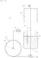
- Fig. 1 is a diagram illustrating an example of a producing process of forming an insulating film on a conductive wire 101 by the electrodeposition coating device 100.
- An anode 104 which is connected to a positive electrode of a direct current power source 103 is disposed on a conductive wire 101a having a circular sectional surface which is wound into the shape of a cylinder.
- the circular conductive wire 101a is pulled up in a direction of an arrow 105 and passes through each step.
- the circular conductive wire 101a is rolled into the shape of a rectangle through a pair of rolling rollers 106, and thus, the rectangular conductive wire 101b having a rectangular sectional surface is obtained.
- the rectangular conductive wire 101b passes through an electrodeposition tank 107 filled with the electrodeposition coating material 102 in which the organic solvent is added to a solvent containing polyamide imide.
- a cathode 108 which is connected to a negative electrode of the direct current power source 103 is disposed around the rectangular conductive wire 101b passing through the electrodeposition tank 107.
- the rectangular conductive wire 101b pulled up from the electrodeposition tank 107 passes through a baking furnace 109, and polyamide imide which has been subjected to the electrodeposition is baked on the rectangular conductive wire 101b, and thus, an insulating conductive wire is formed.
- the "insulating conductive wire” indicates a conductive wire in which an insulating film is formed on a surface. Examples of the conductive wire include a copper wire, an aluminum wire, a copper wire, a copper alloy wire, and the like.
- the temperature of the electrodeposition coating material 102 is 5°C to 60°C
- a concentration of polyamide imide is 1 to 40% by mass
- a direct current voltage is 1 to 300 V
- an energizing time is 0.01 to 30 seconds
- a baking temperature is 200°C to 600°C.
- the concentration of the organic solvent the lower limit is set to the extent of not generating a crack in the insulating film
- the upper limit may be set to a value to the extent of not making film formation according to the electrodeposition difficult due to a decrease in conductivity of the electrodeposition coating material, and a range of approximately 1 to 70% by mass is preferable.
- an organic solvent having a boiling point of higher than or equal to 100°C is selected as the organic solvent. This is because the electrodeposition coating material containing water and polyamide imide is used, and thus, water is initially evaporated at the time of performing baking, that is, in a case where the organic solvent is evaporated before water, it is not possible to expect the swelling and dissolving effect of polyamide imide due to the organic solvent at the time of performing baking. In the swelling, the organic solvent enters between the polymer chains configuring polyamide imide, and polyamide imide is swollen and gelated, and thus, an effect of improving a viscosity is expected.
- the organic solvent enters between the polymer chains, and the polymer chains are rarely bonded to each other, and thus, an effect of dissolving polyamide imide is also expected.
- polyamide imide is dissolved by the organic solvent, and thus, curing does not to start from an original curing temperature of polyamide imide of 80°C, and even after moisture is evaporated, it is possible to perform baking in a state where polyamide imide which is dissolved without being cured is evenly attached onto the surface of the conductive wire as a fluid.
- an organic solvent having excellent solubility with respect to polyamide imide is selected based on a Hansen solubility parameter.
- polyamide imide powder and various organic solvents are mixed, and thus, a solution including 1% by mass each of polyamide imide and the organic solvent is prepared. Respective solutions are classified into a group of a transparent liquid in which the powder is gelated and a group of an opaque liquid in which the powder is precipitated.
- a dispersion term dD S , a polarization term dP S , and a hydrogen bonding term dH S of a Hansen solubility parameter of each organic solvent are formed into a three-dimensional graph, a sphere having a minimum radius is prepared such that the group of the transparent liquid is on the inside and the group of the opaque liquid is on the outside, and the center of the sphere is estimated as a Hansen solubility parameter of polyamide imide.
- D S ⁇ P dD S ⁇ dD P 2 + dP S ⁇ dP P S + dH S ⁇ dH P 2 1 / 2
- dD S is a dispersion component having an HSP value of an organic solvent
- dD P is a dispersion component of an HSP value of polyamide imide
- dP S is a polarization component of an HSP value of an organic solvent
- dP P is an polarization component of an HSP value of an polyamide imide
- dH S is a hydrogen bonding component of an HSP value of an organic solvent
- dH P is a hydrogen bonding component of an HSP value of polyamide imide.
- a rectangular copper wire having a width of 2 mm and a thickness of 0.1 mm was set to an anode of electrodeposition, the rectangular copper wire, and an electrodeposition tank was prepared into which an electrodeposition coating material obtained by adding N,N-dimethyl formamide (DMF) of 6% by mass to polyamide imide (water dispersible polyamide imide varnish) of 5% by mass as an organic solvent was put.
- DMF N,N-dimethyl formamide
- polyamide imide water dispersible polyamide imide varnish
- the rectangular copper wire passed through the electrodeposition tank at a linear velocity of 15 m/min for 2 seconds in a state where a direct current voltage of 5 V was applied, and then, the rectangular copper wire which had been subjected to electrodeposition was allowed to pass through a baking furnace in an atmosphere of 300°C, and was subjected to a baking treatment, and thus, an insulating copper wire having an insulating film thickness of 0.01 mm was prepared.
- An insulating copper wire having an insulating film thickness of 0.01 mm was prepared by the same method as that in Example 1 except that the organic solvent was changed to dimethyl sulfoxide (DMSO) of 6% by mass.
- DMSO dimethyl sulfoxide
- An insulating copper wire having an insulating film thickness of 0.01 mm was prepared by the same method as that in Example 1 except that the organic solvent was changed to 4-butyrolactone (4B) of 6% by mass.
- An insulating copper wire having an insulating film thickness of 0.01 mm was prepared by the same method as that in Example 1 except that the organic solvent was changed to N-methyl-2-pyrrolidone (NMP) of 6% by mass.
- NMP N-methyl-2-pyrrolidone
- An insulating copper wire having an insulating film thickness of 0.01 mm was prepared by the same method as that in Example 1 except that the organic solvent was changed to DMF of 0.5% by mass.
- An insulating copper wire having an insulating film thickness of 0.01 mm was prepared by the same method as that in Example 1 except that the organic solvent was changed to DMF of 50% by mass.
- An insulating copper wire having an insulating film thickness of 0.01 mm was prepared by the same method as that in Example 1 except that the organic solvent was not added, but mist of DMF was added to the rectangular copper wire after the rectangular copper wire passed through the electrodeposition tank.
- An insulating copper wire having an insulating film thickness of 0.01 mm was prepared by the same method as that in Example 1 except that the organic solvent was not added.
- An insulating copper wire having an insulating film thickness of 0.01 mm was prepared by the same method as that in Example 1 except that the organic solvent was changed to formamide of 6% by mass.
- An insulating copper wire having an insulating film thickness of 0.01 mm was prepared by the same method as that in Example 1 except that the organic solvent was changed to acetone of 6% by mass.
- the number of pinholes was evaluated by an SEM picture
- surface roughness Ra was evaluated by a surface step profiler (using a stylus type surface shape measuring instrument manufactured by ULVAC, Inc.)
- voltage resistance was evaluated (using an AC voltage resistance tester TOS5000 manufactured by KIKUSUI ELECTRONICS CORP.). The evaluation results are shown in Table 1.
- Examples 1 to 6 the insulating copper wires having excellent insulating properties were obtained in which any crack or any pinhole was not generated, the surface roughness was 40 to 50 nm, and the voltage resistance was 1.5 kV.
- Example 1 As illustrated in Fig. 2 and Fig. 3 , in Example 1, any pinhole was not observed, whereas in Comparative Example 1, a plurality of pinholes were observed.
- electrodeposition baking is performed by using the electrodeposition coating material simply prepared by using the organic solvent which had a boiling point of higher than or equal to 100°C and was selected by the Hansen solubility parameter, and thus, it was possible to obtain an insulating copper wire including an insulating film which had a dense and smooth surface and high voltage resistance without any pinhole in a safe producing environment.
- the electrodeposition coated article of the present invention in a personal computer, a power inductor for a power source of a smart phone, a transformer of an on-vehicle inverter, and the like.
Landscapes
- Chemical & Material Sciences (AREA)
- Chemical Kinetics & Catalysis (AREA)
- Organic Chemistry (AREA)
- Engineering & Computer Science (AREA)
- Materials Engineering (AREA)
- Electrochemistry (AREA)
- Metallurgy (AREA)
- Life Sciences & Earth Sciences (AREA)
- Wood Science & Technology (AREA)
- Health & Medical Sciences (AREA)
- Molecular Biology (AREA)
- Physics & Mathematics (AREA)
- Spectroscopy & Molecular Physics (AREA)
- Paints Or Removers (AREA)
Abstract
Description
- The present invention relates to an electrodeposition coated article in which an article to be coated is coated with polyamide imide by electrodeposition coating, and a method for producing the same. Furthermore, priority is claimed on Japanese Patent Application No.
171210 filed on August 26, 2014 JP2014-171210 JP2014-171210 - Conventionally, dip coating in which an article to be coated is dipped in a coating material and then is pulled up, and after that, the coating material is dried, and coating is repeated until a predetermined insulating film thickness is obtained, or electrodeposition coating in which a current is allowed to pass through an electrodeposition coating material by inserting an electrode into the electrodeposition coating material, coating material particles are deposited on a rectangular conductive wire which is set to an anode, a formed insulating film is half-cured and rolled, and then, is cured, and thus, an insulating conductive wire is formed is performed as a method of forming an insulating film on a sectional rectangular (hereinafter, also simply referred to as "rectangular") conductive wire (for example, refer to Patent Document 1). On the other hand, a method is disclosed as the electrodeposition coating in which a rectangular conductive wire is allowed to pass through an electrodeposition layer filled with an electrodeposition coating material, and then, is allowed to pass through a solvent layer filled with an organic solvent or mist or steam of an organic solvent, and after that, is baked, and thus, an insulating film is formed (for example, refer to Patent Document 2). Further, a method of generating mist of an organic solvent by a ultrasonic wave or a method of spraying steam of an organic solvent from an ejection nozzle is disclosed as a method of electrodeposition coating a rectangular conductive wire with an electrodeposition coating material, and then, of spraying an organic solvent (for example, refer to Patent Documents 3 and 4).
- Patent Documents
-
- [Patent Document 1] Japanese Unexamined Patent Application Publication No.
H03-159014 Page 1 to Upper Right Column on Page 2) - [Patent Document 2] Japanese Unexamined Patent Application Publication No.
H03-241609 - [Patent Document 3] Japanese Examined Patent Application Publication No.
H04-065159 - [Patent Document 4] Japanese Unexamined Patent Application Publication No.
2012-160304 - However, in the conventional dip coating described in the
Patent Document 1 mentioned above, it is difficult to attach the coating material to a corner portion of the rectangular conductive wire, uneven coating occurs, or the coating is required to be repeated many times in order to obtain a predetermined insulating film thickness, and in the electrodeposition coating, an electric field is concentrated on the corner portion of the rectangular conductive wire, and thus, the insulating film on the corner portion becomes thick, or rolling is required to be performed in a half-cured state. On the other hand, in the conventional method of allowing the rectangular conductive wire to pass through the organic solvent described in the Patent Document 2 mentioned above, an insulating film not having a pinhole is obtained with an equal thickness of insulating film, but even in a case of being dipped in a liquid of the organic solvent, the liquid does not penetrate into a gap between resin fine particles due to a surface tension, and thus, it is not possible to perform sufficient dissolution, or it is difficult to control the temperature or the amount of the organic solvent in the steam or the mist. Further, in the conventional methods of generating the mist of the organic solvent by the ultrasonic wave or the method of spraying the steam of the organic solvent from the ejection nozzle described in the Patent Documents 3 and 4 mentioned above, it is possible to adjust the temperature or the amount of the organic solvent, but a complicated device configuration such as a ultrasonic wave generating device, a steam spraying device using a nozzle, and other control devices is required to be controlled, there is a concern that the organic solvent is discharged into the air and affects a human body, and thus, fire protection is required to be considered. - An object of the present invention is to provide an electrodeposition coated article in which an insulating film does not have a pinhole and insulating properties are excellent. Another object of the present invention is to provide a method for producing an electrodeposition coated article in which it is possible to simply form an insulating film having a flat surface without any pinhole in a safe environment.
- As a result of intensive studies for attaining the objects described above, the inventors have found that in a case where a base material is coated with an insulating film by electrodeposition coating, an organic solvent having high polyamide imide solubility is added to an electrodeposition coating material containing polyamide imide, and the electrodeposition coating is performed, and thus, it is possible to form an insulating film having a flat surface without any pinhole, and thus, the present invention has been completed.
- The first viewpoint of the present invention is a method for producing an electrodeposition coated article, in which an insulating film is formed by forming an insulating layer on a surface of an article to be coated according to an electrodeposition method by using an electrodeposition coating material, and then by performing a baking treatment, in which the electrodeposition coating material contains a solvent containing polyamide imide and an organic solvent added to the electrodeposition coating material, and a boiling point of the organic solvent is higher than 100°C, and a relationship of D(S-P) < 6 is satisfied, D(S-P) being represented by an expression described below.

- Here, dDS is a dispersion component of a Hansen solubility parameter (HSP) value of an organic solvent, dDP is a dispersion component of an HSP value of polyamide imide, dPS is a polarization component of an HSP value of an organic solvent, dPP is an polarization component of an HSP value of an polyamide imide, dHS is a hydrogen bonding component of an HSP value of an organic solvent, and dHP is a hydrogen bonding component of an HSP value of polyamide imide. HSP (dD, dP, and dH) is a value intrinsic to a substance, and compatibility is high among the substances with the close values to one another. It is possible to calculate the value from a molecular structure and to estimate the value by a method of a second viewpoint of the present invention described below even in a case where the molecular structure of the substance is not known.
- The second viewpoint of the present invention is an invention based on the first viewpoint, wherein a case in which a mixed liquid of the polyamide imide and the organic solvent becomes transparent is set to an organic solvent having solubility with respect to the polyamide imide, a case in which a mixed liquid of the polyamide imide and the organic solvent becomes opaque is set to an organic solvent not having solubility with respect to the polyamide imide, dDS, dPS, and dHS of the organic solvent are formed into a three-dimensional graph, a center of a minimum sphere on which all points indicating the organic solvent having solubility with respect to the polyamide imide enter is estimated as dDP, dPP, and dHP of the polyamide imide, and an organic solvent satisfying the relationship of D(S-P) < 6 is selected.
- The third viewpoint of the present invention is an invention based on the first viewpoint or the second viewpoint, wherein the electrodeposition coating material is water dispersible or water soluble, and the organic solvent is a hydrophilic solvent.
- The fourth viewpoint of the present invention is an invention based on the first viewpoint to the third viewpoint, wherein the organic solvent is N,N-dimethyl acetamide, N,N-dimethyl formamide, propylene carbonate, dimethyl sulfoxide, 4-butyrolactone, or N-methyl-2-pyrrolidone.
- The fifth viewpoint of the present invention is an invention based on the first viewpoint to the fourth viewpoint, wherein the article to be coated is a copper wire.
- The sixth viewpoint of the present invention is an electrodeposition coated article, in which in an insulating film formed on a surface of an article to be coated, the number of pinholes on a film sectional surface measured by being observed with SEM is less than or equal to 50 items/10 µm square, and surface roughness Ra measured according to JISC0601 is less than or equal to 40 nm.
- The seventh viewpoint of the present invention is an invention based on the sixth viewpoint, the article to be coated is a copper wire.
- In the first viewpoint of the present invention, the organic solvent is added to the electrodeposition coating material which is a solvent containing polyamide imide, and thus, a tank of an organic solvent, a device of generating and spraying mist and steam, and a control device are not required, and the organic solvent is not formed into the steam or the mist, and thus, it is possible to simply produce in a safe environment by decreasing a concern that the organic solvent is discharged into the air. Next, the boiling point of the organic solvent is 100°C or higher, and thus, even in a case where a temperature in a baking step becomes 100°C or higher, and the moisture of the electrodeposition coating material is evaporated, the organic solvent remains. Therefore, it is possible to expect a swelling and dissolving effect of polyamide imide with respect to a resin due to the organic solvent for a long period of time. Further, solubility of the organic solvent with respect to polyamide imide is defined by an expression of D(S-P) < 6 by using a Hansen solubility parameter. In a case where an organic solvent having low compatibility with respect to polyamide imide is added, it is difficult for organic solvent molecules to enter a polymer chain forming polyamide imide particles, and a state is not formed in which the polymer chain is released, and thus, film formability is not improved, and a crack or a pinhole may be generated. However, the organic solvent having high compatibility with respect to polyamide imide is selected and added by the prescribed conditions described above, and thus, the polyamide imide particles are in a swollen state, that is, the organic solvent molecules enter the polymer chain forming the polyamide imide particles, the state is formed in which the polymer chain is released, and the polyamide imide particles are easily fused together at the time of performing thermal curing, and film formability is improved. Therefore, it is possible to produce an electrodeposition coated article including a flat insulating film having excellent insulating properties without any crack or any pinhole.
- In the second viewpoint of the present invention, a case in which the mixed liquid of the polyamide imide and the organic solvent becomes transparent is set to the organic solvent having solubility with respect to the polyamide imide, a case in which a mixed liquid of the polyamide imide and the organic solvent becomes opaque is set to an organic solvent not having solubility with respect to the polyamide imide, dDS, dPS, and dHS of the organic solvent are formed into the three-dimensional graph, the center of the minimum sphere on which all of the points indicating the organic solvent having solubility with respect to a polymer enter is estimated as dDP, dPP, and dHP of the polyamide imide, and it is possible to select the organic solvent satisfying the relationship of D(S-P) < 6.
- In the third viewpoint of the present invention, the electrodeposition coating material is water dispersible or water soluble, and the organic solvent is the hydrophilic solvent, and thus, the electrodeposition coating material and the organic solvent become substances which are dispersed or dissolved in water. Therefore, it is possible to reliably form an insulating film on a surface to be coated.
- In the fourth viewpoint of the present invention, N,N-dimethyl acetamide, N,N-dimethyl formamide, propylene carbonate, dimethyl sulfoxide, 4-butyrolactone, or N-methyl-2-pyrrolidone is used as the organic solvent, and thus, it is possible to form an insulating film having an even surface with few pinholes or without any pinhole, in particular, with respect to an epoxy polymer and an acrylic polymer.
- In the fifth viewpoint of the present invention, it is possible to form an insulating copper wire in which the insulating film has few pinholes or does not have a pinhole.
- In the sixth viewpoint of the present invention, it is possible to provide an electrodeposition coated article including the insulating film with few pinholes or without any pinhole in which insulating properties are excellent, and it is possible to maintain insulating performance even in a rigorous environment where irradiation of an electron beam, a cosmic ray, an ultraviolet ray, and the like is strictly performed.
- In the seventh viewpoint of the present invention, it is possible to provide an insulating copper wire in which the insulating film has few pinholes or does not have a pinhole, insulating properties are excellent, and it is possible to maintain insulating performance even in a rigorous environment where irradiation of an electron beam, a cosmic ray, an ultraviolet ray, and the like is strictly performed.
-
-
Fig. 1 is a diagram schematically illustrating an electrodeposition coating device of an embodiment of the present invention. -
Fig. 2 is an SEM picture diagram in which a sectional surface of an insulating portion of an insulating copper wire of Example 1 is enlarged. -
Fig. 3 is an SEM picture diagram in which a sectional surface of an insulating portion of an insulating copper wire of Comparative Example 1 is enlarged. - Next, an embodiment of the present invention will be described on the basis of the drawings.
- As illustrated in
Fig. 1 , the present invention is a method in which a rectangularconductive wire 101b is coated with polyamide imide and an organic solvent by anelectrodeposition coating device 100, and the coated rectangularconductive wire 101b is subjected to a heat treatment, and thus, an insulating conductive wire which is an electrodeposition coated article including an insulating film of cured polyamide imide is formed on a surface is produced. - In the characteristic configuration of the present invention, an
electrodeposition coating material 102 which is prepared by adding a predetermined organic solvent selected by a selection method using a known Hansen solubility parameter described below to an electrodeposition coating material made from a solvent containing polyamide imide is used as a coating material of anelectrodeposition coating device 100. Thus, theelectrodeposition coating material 102 containing the organic solvent is set to a coating material of electrodeposition coating, and thus, it is possible to simply prepare theelectrodeposition coating material 102 which forms a desired insulating film, and it is possible to perform the electrodeposition coating without separately providing a step of applying the organic solvent. - A producing process of an electrodeposition coated article of the present invention will be described in detail with reference to
Fig. 1. Fig. 1 illustrates a mode of performing an electrodeposition step, a baking step, and the like continuously in a vertical direction, but it is possible to perform the electrodeposition coating of the present invention by any mode such as a method of performing each step continuously in a horizontal direction or a batch mode of collectively performing one step, and then, of performing the next step. -
Fig. 1 is a diagram illustrating an example of a producing process of forming an insulating film on a conductive wire 101 by theelectrodeposition coating device 100. Ananode 104 which is connected to a positive electrode of a directcurrent power source 103 is disposed on aconductive wire 101a having a circular sectional surface which is wound into the shape of a cylinder. The circularconductive wire 101a is pulled up in a direction of anarrow 105 and passes through each step. First, as a first step, the circularconductive wire 101a is rolled into the shape of a rectangle through a pair ofrolling rollers 106, and thus, the rectangularconductive wire 101b having a rectangular sectional surface is obtained. Next, as a second step, the rectangularconductive wire 101b passes through anelectrodeposition tank 107 filled with theelectrodeposition coating material 102 in which the organic solvent is added to a solvent containing polyamide imide. In theelectrodeposition coating material 102 of theelectrodeposition tank 107, acathode 108 which is connected to a negative electrode of the directcurrent power source 103 is disposed around the rectangularconductive wire 101b passing through theelectrodeposition tank 107. When the rectangularconductive wire 101b passes through theelectrodeposition tank 107, a direct current voltage is applied by the directcurrent power source 103, and dissolved polyamide imide is subjected to electrodeposition on the surface of the rectangularconductive wire 101b. Next, as a third step, the rectangularconductive wire 101b pulled up from theelectrodeposition tank 107 passes through abaking furnace 109, and polyamide imide which has been subjected to the electrodeposition is baked on the rectangularconductive wire 101b, and thus, an insulating conductive wire is formed. Furthermore, in this specification, the "insulating conductive wire" indicates a conductive wire in which an insulating film is formed on a surface. Examples of the conductive wire include a copper wire, an aluminum wire, a copper wire, a copper alloy wire, and the like. - It is preferable that the temperature of the
electrodeposition coating material 102 is 5°C to 60°C, a concentration of polyamide imide is 1 to 40% by mass, a direct current voltage is 1 to 300 V, an energizing time is 0.01 to 30 seconds, and a baking temperature is 200°C to 600°C. Furthermore, in the concentration of the organic solvent, the lower limit is set to the extent of not generating a crack in the insulating film, the upper limit may be set to a value to the extent of not making film formation according to the electrodeposition difficult due to a decrease in conductivity of the electrodeposition coating material, and a range of approximately 1 to 70% by mass is preferable. - Here, the selection method of the organic solvent of the present invention will be described in detail.
- First, an organic solvent having a boiling point of higher than or equal to 100°C is selected as the organic solvent. This is because the electrodeposition coating material containing water and polyamide imide is used, and thus, water is initially evaporated at the time of performing baking, that is, in a case where the organic solvent is evaporated before water, it is not possible to expect the swelling and dissolving effect of polyamide imide due to the organic solvent at the time of performing baking. In the swelling, the organic solvent enters between the polymer chains configuring polyamide imide, and polyamide imide is swollen and gelated, and thus, an effect of improving a viscosity is expected. In addition, the organic solvent enters between the polymer chains, and the polymer chains are rarely bonded to each other, and thus, an effect of dissolving polyamide imide is also expected. This is because polyamide imide is dissolved by the organic solvent, and thus, curing does not to start from an original curing temperature of polyamide imide of 80°C, and even after moisture is evaporated, it is possible to perform baking in a state where polyamide imide which is dissolved without being cured is evenly attached onto the surface of the conductive wire as a fluid.
- Next, an organic solvent having excellent solubility with respect to polyamide imide is selected based on a Hansen solubility parameter.
- First, polyamide imide powder and various organic solvents are mixed, and thus, a solution including 1% by mass each of polyamide imide and the organic solvent is prepared. Respective solutions are classified into a group of a transparent liquid in which the powder is gelated and a group of an opaque liquid in which the powder is precipitated. Next, a dispersion term dDS, a polarization term dPS, and a hydrogen bonding term dHS of a Hansen solubility parameter of each organic solvent are formed into a three-dimensional graph, a sphere having a minimum radius is prepared such that the group of the transparent liquid is on the inside and the group of the opaque liquid is on the outside, and the center of the sphere is estimated as a Hansen solubility parameter of polyamide imide. An organic solvent in which a value obtained by inputting the estimated Hansen solubility parameter of polyamide imide and the Hansen solubility parameter of the organic solvent into Expression (1) described below is D(S-P) < 6 is selected as an organic solvent having excellent solubility with respect to polyamide imide.

- Here, dDS is a dispersion component having an HSP value of an organic solvent, dDP is a dispersion component of an HSP value of polyamide imide, dPS is a polarization component of an HSP value of an organic solvent, dPP is an polarization component of an HSP value of an polyamide imide, dHS is a hydrogen bonding component of an HSP value of an organic solvent, and dHP is a hydrogen bonding component of an HSP value of polyamide imide.
- Next, examples of the present invention will be described in detail along with comparative examples.
- A rectangular copper wire having a width of 2 mm and a thickness of 0.1 mm was set to an anode of electrodeposition, the rectangular copper wire, and an electrodeposition tank was prepared into which an electrodeposition coating material obtained by adding N,N-dimethyl formamide (DMF) of 6% by mass to polyamide imide (water dispersible polyamide imide varnish) of 5% by mass as an organic solvent was put. Next, the rectangular copper wire passed through the electrodeposition tank at a linear velocity of 15 m/min for 2 seconds in a state where a direct current voltage of 5 V was applied, and then, the rectangular copper wire which had been subjected to electrodeposition was allowed to pass through a baking furnace in an atmosphere of 300°C, and was subjected to a baking treatment, and thus, an insulating copper wire having an insulating film thickness of 0.01 mm was prepared.
- <Example 2>
- An insulating copper wire having an insulating film thickness of 0.01 mm was prepared by the same method as that in Example 1 except that the organic solvent was changed to dimethyl sulfoxide (DMSO) of 6% by mass.
- An insulating copper wire having an insulating film thickness of 0.01 mm was prepared by the same method as that in Example 1 except that the organic solvent was changed to 4-butyrolactone (4B) of 6% by mass.
- An insulating copper wire having an insulating film thickness of 0.01 mm was prepared by the same method as that in Example 1 except that the organic solvent was changed to N-methyl-2-pyrrolidone (NMP) of 6% by mass.
- An insulating copper wire having an insulating film thickness of 0.01 mm was prepared by the same method as that in Example 1 except that the organic solvent was changed to DMF of 0.5% by mass.
- An insulating copper wire having an insulating film thickness of 0.01 mm was prepared by the same method as that in Example 1 except that the organic solvent was changed to DMF of 50% by mass.
- An insulating copper wire having an insulating film thickness of 0.01 mm was prepared by the same method as that in Example 1 except that the organic solvent was not added, but mist of DMF was added to the rectangular copper wire after the rectangular copper wire passed through the electrodeposition tank.
- An insulating copper wire having an insulating film thickness of 0.01 mm was prepared by the same method as that in Example 1 except that the organic solvent was not added.
- An insulating copper wire having an insulating film thickness of 0.01 mm was prepared by the same method as that in Example 1 except that the organic solvent was changed to formamide of 6% by mass.
- An insulating copper wire having an insulating film thickness of 0.01 mm was prepared by the same method as that in Example 1 except that the organic solvent was changed to acetone of 6% by mass.
- In the insulating copper wires obtained in each of the examples and the comparative examples, the number of pinholes was evaluated by an SEM picture, surface roughness Ra was evaluated by a surface step profiler (using a stylus type surface shape measuring instrument manufactured by ULVAC, Inc.), and voltage resistance was evaluated (using an AC voltage resistance tester TOS5000 manufactured by KIKUSUI ELECTRONICS CORP.). The evaluation results are shown in Table 1.
[Table 1] Additive Evaluation Item Type Amount (% by mass) Boiling Point (°C) D(S-P) Presence or Absence of Crack Surface Roughness Ra (nm) Pinhole (Item/10 µm Square) Voltage Resistance (kV) Example 1 DMF 6 153 3.8 Absent 50 0 1.5 Example 2 DMSO 6 189 2.7 Absent 40 0 1.5 Example 3 4B 6 204 4.5 Absent 40 0 1.5 Example 4 NMP 6 202 2.6 Absent 50 0 1.5 Example 5 DMF 0.5 153 3.8 Absent 50 0 1.5 Example 6 DMF 50 153 3.8 Absent 50 0 1.5 Comparative Example 1 DMF Mist Treatment - 153 3.8 Absent 250 16 1.5 Comparative Example 2 Not being Added - - - Present - - - Comparative Example 3 Formamide 6 211 18.6 Absent 200 50 0.3 Comparative Example 4 Acetone 6 57 5.8 Present - - - - In Examples 1 to 6, the insulating copper wires having excellent insulating properties were obtained in which any crack or any pinhole was not generated, the surface roughness was 40 to 50 nm, and the voltage resistance was 1.5 kV.
- In Comparative Examples 1 and 3, any crack was not generated, but the surface roughness was 200 to 250 nm, the number of pinholes was 16 to 50 items/10 µm square, and the voltage resistance was 0.3 to 1.5 kV, and thus, each evaluation item had an inferior result, compared to the examples.
- In both of Comparative Examples 2 and 4, a crack was generated, and in the other evaluation items, data for comparative evaluation was not obtained.
- Next, the state of the structure on the sectional surface of the insulating copper wires of Example 1 and Comparative Example 1 was observed by an SEM picture. The SEM picture was imaged by using S-4300SE manufactured by Hitachi, Ltd. The results are illustrated in
Fig. 2 andFig. 3 . - As illustrated in
Fig. 2 andFig. 3 , in Example 1, any pinhole was not observed, whereas in Comparative Example 1, a plurality of pinholes were observed. - From the results described above, it was confirmed that electrodeposition baking is performed by using the electrodeposition coating material simply prepared by using the organic solvent which had a boiling point of higher than or equal to 100°C and was selected by the Hansen solubility parameter, and thus, it was possible to obtain an insulating copper wire including an insulating film which had a dense and smooth surface and high voltage resistance without any pinhole in a safe producing environment.
- It is possible to use the electrodeposition coated article of the present invention in a personal computer, a power inductor for a power source of a smart phone, a transformer of an on-vehicle inverter, and the like.
-
- 102: electrodeposition coating material
Claims (7)
- A method for producing an electrodeposition coated article, in which an insulating film is formed by forming an insulating layer on a surface of an article to be coated according to an electrodeposition method by using an electrodeposition coating material, and then by performing a baking treatment,
wherein the electrodeposition coating material contains a solvent containing the polyamide imide and an organic solvent added to the electrodeposition coating material, and
a boiling point of the organic solvent is higher than 100°C, and a relationship of D(S-P) < 6 is satisfied, D(S-P) being represented by an expression described below,
- The method for producing an electrodeposition coated article according to Claim 1,
wherein a case in which a mixed liquid of the polyamide imide and the organic solvent becomes transparent is set to an organic solvent having solubility with respect to the polyamide imide, a case in which a mixed liquid of the polyamide imide and the organic solvent becomes opaque is set to an organic solvent not having solubility with respect to the polyamide imide, dDS, dPS, and dHS of the organic solvent are formed into a three-dimensional graph, a center of a minimum sphere on which all points indicating the organic solvent having solubility with respect to the polyamide imide enter is estimated as dDP, dPP, and dHP of the polyamide imide, and an organic solvent satisfying the relationship of D(S-P) < 6 is selected. - The method for producing an electrodeposition coated article according to Claim 1 or 2,
wherein the electrodeposition coating material is water dispersible or water soluble, and the organic solvent is a hydrophilic solvent. - The method for producing an electrodeposition coated article according to any one of Claims 1 to 3,
wherein the organic solvent is N,N-dimethyl acetamide, N,N-dimethyl formamide, propylene carbonate, dimethyl sulfoxide, 4-butyrolactone, or N-methyl-2-pyrrolidone. - The method for producing an electrodeposition coated article according to any one of Claims 1 to 4,
wherein the article to be coated is a copper wire. - An electrodeposition coated article,
wherein in an insulating film formed on a surface of an article to be coated, the number of pinholes on a film sectional surface measured by being observed with SEM is less than or equal to 50 items/10 µm square, and surface roughness Ra measured according to JISC0601 is less than or equal to 40 nm. - The electrodeposition coated article according to Claim 6,
wherein the article to be coated is a copper wire.
Applications Claiming Priority (2)
| Application Number | Priority Date | Filing Date | Title |
|---|---|---|---|
| JP2014171210A JP6412740B2 (en) | 2014-08-26 | 2014-08-26 | Method for producing electrodeposited body |
| PCT/JP2015/071600 WO2016031480A1 (en) | 2014-08-26 | 2015-07-30 | Electrodeposition coated article and method for producing same |
Publications (3)
| Publication Number | Publication Date |
|---|---|
| EP3187628A1 true EP3187628A1 (en) | 2017-07-05 |
| EP3187628A4 EP3187628A4 (en) | 2018-04-04 |
| EP3187628B1 EP3187628B1 (en) | 2021-03-17 |
Family
ID=55399381
Family Applications (1)
| Application Number | Title | Priority Date | Filing Date |
|---|---|---|---|
| EP15835515.6A Active EP3187628B1 (en) | 2014-08-26 | 2015-07-30 | Electrodeposition coated article and method for producing same |
Country Status (7)
| Country | Link |
|---|---|
| US (1) | US20170267874A1 (en) |
| EP (1) | EP3187628B1 (en) |
| JP (1) | JP6412740B2 (en) |
| KR (1) | KR102352646B1 (en) |
| CN (1) | CN106536792B (en) |
| TW (1) | TWI671765B (en) |
| WO (1) | WO2016031480A1 (en) |
Families Citing this family (2)
| Publication number | Priority date | Publication date | Assignee | Title |
|---|---|---|---|---|
| US11230788B2 (en) | 2016-02-18 | 2022-01-25 | Mitsubishi Materials Corporation | Electrodeposition liquid and electrodeposition-coated article |
| JP6859736B2 (en) * | 2017-02-16 | 2021-04-14 | 三菱マテリアル株式会社 | Electrodeposition liquid and method for manufacturing a conductor with an insulating film using this |
Family Cites Families (13)
| Publication number | Priority date | Publication date | Assignee | Title |
|---|---|---|---|---|
| JPS5230846A (en) * | 1975-09-03 | 1977-03-08 | Mitsubishi Electric Corp | Method for electrodeposition coating |
| JP2649979B2 (en) | 1989-11-15 | 1997-09-03 | 三菱電線工業株式会社 | Manufacturing method of rectangular insulated wire |
| JPH07120491B2 (en) | 1990-02-20 | 1995-12-20 | 三菱電線工業株式会社 | Flat ultra-thin insulated wire |
| JPH0465159A (en) | 1990-07-05 | 1992-03-02 | Oki Electric Ind Co Ltd | Manufacture of capacitor |
| JP5441802B2 (en) * | 2009-05-26 | 2014-03-12 | 関西ペイント株式会社 | Cationic electrodeposition coating composition |
| JP5449012B2 (en) * | 2010-05-06 | 2014-03-19 | 古河電気工業株式会社 | Insulated wire, electrical equipment, and method of manufacturing insulated wire |
| WO2011152364A1 (en) * | 2010-05-31 | 2011-12-08 | 日立化成工業株式会社 | Modified polyamideimide resin, electrically insulating material, method for improving dielectric breakdown resistance of insulating layer, and insulated wire |
| JP5377535B2 (en) * | 2011-01-31 | 2013-12-25 | 三菱電線工業株式会社 | Insulated wire manufacturing method and manufacturing apparatus |
| JP5609732B2 (en) * | 2011-03-22 | 2014-10-22 | 日立金属株式会社 | Insulating paint and insulated wire using the same |
| US10406791B2 (en) * | 2011-05-12 | 2019-09-10 | Elantas Pdg, Inc. | Composite insulating film |
| CN103299397B (en) * | 2011-07-19 | 2014-07-16 | 三菱丽阳株式会社 | Manufacturing method of mold for nanoimprinting |
| CA2864071C (en) * | 2012-03-07 | 2017-08-01 | Furukawa Electric Co., Ltd. | Insulated wire having a layer containing bubbles, electrical equipment, and method of producing insulated wire having a layer containing bubbles |
| JP6069035B2 (en) * | 2013-03-07 | 2017-01-25 | 三菱マテリアル株式会社 | Method for producing electrodeposited body |
-
2014
- 2014-08-26 JP JP2014171210A patent/JP6412740B2/en active Active
-
2015
- 2015-07-30 EP EP15835515.6A patent/EP3187628B1/en active Active
- 2015-07-30 US US15/505,157 patent/US20170267874A1/en not_active Abandoned
- 2015-07-30 WO PCT/JP2015/071600 patent/WO2016031480A1/en not_active Ceased
- 2015-07-30 CN CN201580038396.1A patent/CN106536792B/en active Active
- 2015-07-30 KR KR1020177001327A patent/KR102352646B1/en active Active
- 2015-08-10 TW TW104125939A patent/TWI671765B/en active
Also Published As
| Publication number | Publication date |
|---|---|
| KR102352646B1 (en) | 2022-01-17 |
| EP3187628A4 (en) | 2018-04-04 |
| KR20170048316A (en) | 2017-05-08 |
| CN106536792B (en) | 2019-08-16 |
| TW201611041A (en) | 2016-03-16 |
| CN106536792A (en) | 2017-03-22 |
| JP2016044348A (en) | 2016-04-04 |
| JP6412740B2 (en) | 2018-10-24 |
| TWI671765B (en) | 2019-09-11 |
| WO2016031480A1 (en) | 2016-03-03 |
| US20170267874A1 (en) | 2017-09-21 |
| EP3187628B1 (en) | 2021-03-17 |
Similar Documents
| Publication | Publication Date | Title |
|---|---|---|
| EP1850353A1 (en) | Conductive film | |
| KR102676821B1 (en) | Electrodeposition solution and electrodeposition coating material | |
| JP2007332224A (en) | Sheet-like composite material and manufacturing method thereof | |
| EP3070719A1 (en) | Conductive paste and method for manufacturing conductive film using same | |
| US11189393B2 (en) | Conductive coated composite body and method for producing same | |
| TW201413750A (en) | Method for producing conductive film and composition for forming conductive film | |
| EP3187628B1 (en) | Electrodeposition coated article and method for producing same | |
| US8968824B2 (en) | Method for producing silver conductive film | |
| JP5614101B2 (en) | Method for manufacturing conductive substrate | |
| Marušić et al. | Influence of gamma irradiation on a fatty acid self-assembling coating of copper | |
| JP6069035B2 (en) | Method for producing electrodeposited body | |
| JP2012174374A (en) | Method for producing conductive coating film and conductive coating film | |
| EP3244420A1 (en) | Electroconductive paste and method for manufacturing electroconductive film using same | |
| JP5905845B2 (en) | Method for manufacturing conductive film and conductive film | |
| US11230788B2 (en) | Electrodeposition liquid and electrodeposition-coated article | |
| JP2015069752A (en) | Conductive paste, metallic thin film, and method for producing the same | |
| Fujimto et al. | Flexible multilayer electrode films consisted of polyaniline and polyelectrolyte by layer-by-layer self-assembly | |
| JP2002298674A (en) | Manufacturing method of insulation wire and insulation wire | |
| JP2012174375A (en) | Method for producing conductive coating film and conductive coating film | |
| Ye et al. | Superhydrophobic behavior of polymer-coated nanowire-arrays as a function of interfacial affinity and etching | |
| CA3080219C (en) | Boron nitride nanotube coated substrates for sintering of metallic traces by intense pulse light | |
| JP6410278B2 (en) | Conductive film forming composition and conductive film manufacturing method | |
| CN114141541B (en) | Electrode foil smooth edge forming method | |
| KR20170117376A (en) | Method for producing insulated wire | |
| JP6746276B2 (en) | Transparent conductive sheet and method for manufacturing the same |
Legal Events
| Date | Code | Title | Description |
|---|---|---|---|
| STAA | Information on the status of an ep patent application or granted ep patent |
Free format text: STATUS: THE INTERNATIONAL PUBLICATION HAS BEEN MADE |
|
| PUAI | Public reference made under article 153(3) epc to a published international application that has entered the european phase |
Free format text: ORIGINAL CODE: 0009012 |
|
| STAA | Information on the status of an ep patent application or granted ep patent |
Free format text: STATUS: REQUEST FOR EXAMINATION WAS MADE |
|
| 17P | Request for examination filed |
Effective date: 20170126 |
|
| AK | Designated contracting states |
Kind code of ref document: A1 Designated state(s): AL AT BE BG CH CY CZ DE DK EE ES FI FR GB GR HR HU IE IS IT LI LT LU LV MC MK MT NL NO PL PT RO RS SE SI SK SM TR |
|
| AX | Request for extension of the european patent |
Extension state: BA ME |
|
| DAV | Request for validation of the european patent (deleted) | ||
| DAX | Request for extension of the european patent (deleted) | ||
| A4 | Supplementary search report drawn up and despatched |
Effective date: 20180307 |
|
| RIC1 | Information provided on ipc code assigned before grant |
Ipc: C25D 13/04 20060101ALI20180301BHEP Ipc: C25D 13/16 20060101ALI20180301BHEP Ipc: H01B 3/30 20060101ALI20180301BHEP Ipc: C09D 5/44 20060101ALI20180301BHEP Ipc: C25D 13/10 20060101ALI20180301BHEP Ipc: C25D 13/06 20060101AFI20180301BHEP Ipc: C09D 179/08 20060101ALI20180301BHEP |
|
| RAP1 | Party data changed (applicant data changed or rights of an application transferred) |
Owner name: MITSUBISHI MATERIALS CORPORATION Owner name: MITSUBISHI CABLE INDUSTRIES, LTD. |
|
| RAP1 | Party data changed (applicant data changed or rights of an application transferred) |
Owner name: MITSUBISHI MATERIALS CORPORATION |
|
| STAA | Information on the status of an ep patent application or granted ep patent |
Free format text: STATUS: EXAMINATION IS IN PROGRESS |
|
| 17Q | First examination report despatched |
Effective date: 20200817 |
|
| GRAP | Despatch of communication of intention to grant a patent |
Free format text: ORIGINAL CODE: EPIDOSNIGR1 |
|
| STAA | Information on the status of an ep patent application or granted ep patent |
Free format text: STATUS: GRANT OF PATENT IS INTENDED |
|
| INTG | Intention to grant announced |
Effective date: 20201120 |
|
| GRAS | Grant fee paid |
Free format text: ORIGINAL CODE: EPIDOSNIGR3 |
|
| GRAA | (expected) grant |
Free format text: ORIGINAL CODE: 0009210 |
|
| STAA | Information on the status of an ep patent application or granted ep patent |
Free format text: STATUS: THE PATENT HAS BEEN GRANTED |
|
| AK | Designated contracting states |
Kind code of ref document: B1 Designated state(s): AL AT BE BG CH CY CZ DE DK EE ES FI FR GB GR HR HU IE IS IT LI LT LU LV MC MK MT NL NO PL PT RO RS SE SI SK SM TR |
|
| REG | Reference to a national code |
Ref country code: GB Ref legal event code: FG4D |
|
| REG | Reference to a national code |
Ref country code: CH Ref legal event code: EP |
|
| REG | Reference to a national code |
Ref country code: DE Ref legal event code: R096 Ref document number: 602015067064 Country of ref document: DE |
|
| REG | Reference to a national code |
Ref country code: IE Ref legal event code: FG4D |
|
| REG | Reference to a national code |
Ref country code: AT Ref legal event code: REF Ref document number: 1372325 Country of ref document: AT Kind code of ref document: T Effective date: 20210415 |
|
| REG | Reference to a national code |
Ref country code: LT Ref legal event code: MG9D |
|
| PG25 | Lapsed in a contracting state [announced via postgrant information from national office to epo] |
Ref country code: NO Free format text: LAPSE BECAUSE OF FAILURE TO SUBMIT A TRANSLATION OF THE DESCRIPTION OR TO PAY THE FEE WITHIN THE PRESCRIBED TIME-LIMIT Effective date: 20210617 Ref country code: FI Free format text: LAPSE BECAUSE OF FAILURE TO SUBMIT A TRANSLATION OF THE DESCRIPTION OR TO PAY THE FEE WITHIN THE PRESCRIBED TIME-LIMIT Effective date: 20210317 Ref country code: HR Free format text: LAPSE BECAUSE OF FAILURE TO SUBMIT A TRANSLATION OF THE DESCRIPTION OR TO PAY THE FEE WITHIN THE PRESCRIBED TIME-LIMIT Effective date: 20210317 Ref country code: GR Free format text: LAPSE BECAUSE OF FAILURE TO SUBMIT A TRANSLATION OF THE DESCRIPTION OR TO PAY THE FEE WITHIN THE PRESCRIBED TIME-LIMIT Effective date: 20210618 Ref country code: BG Free format text: LAPSE BECAUSE OF FAILURE TO SUBMIT A TRANSLATION OF THE DESCRIPTION OR TO PAY THE FEE WITHIN THE PRESCRIBED TIME-LIMIT Effective date: 20210617 |
|
| REG | Reference to a national code |
Ref country code: AT Ref legal event code: MK05 Ref document number: 1372325 Country of ref document: AT Kind code of ref document: T Effective date: 20210317 |
|
| REG | Reference to a national code |
Ref country code: NL Ref legal event code: MP Effective date: 20210317 |
|
| PG25 | Lapsed in a contracting state [announced via postgrant information from national office to epo] |
Ref country code: LV Free format text: LAPSE BECAUSE OF FAILURE TO SUBMIT A TRANSLATION OF THE DESCRIPTION OR TO PAY THE FEE WITHIN THE PRESCRIBED TIME-LIMIT Effective date: 20210317 Ref country code: RS Free format text: LAPSE BECAUSE OF FAILURE TO SUBMIT A TRANSLATION OF THE DESCRIPTION OR TO PAY THE FEE WITHIN THE PRESCRIBED TIME-LIMIT Effective date: 20210317 Ref country code: SE Free format text: LAPSE BECAUSE OF FAILURE TO SUBMIT A TRANSLATION OF THE DESCRIPTION OR TO PAY THE FEE WITHIN THE PRESCRIBED TIME-LIMIT Effective date: 20210317 |
|
| PG25 | Lapsed in a contracting state [announced via postgrant information from national office to epo] |
Ref country code: NL Free format text: LAPSE BECAUSE OF FAILURE TO SUBMIT A TRANSLATION OF THE DESCRIPTION OR TO PAY THE FEE WITHIN THE PRESCRIBED TIME-LIMIT Effective date: 20210317 |
|
| PG25 | Lapsed in a contracting state [announced via postgrant information from national office to epo] |
Ref country code: LT Free format text: LAPSE BECAUSE OF FAILURE TO SUBMIT A TRANSLATION OF THE DESCRIPTION OR TO PAY THE FEE WITHIN THE PRESCRIBED TIME-LIMIT Effective date: 20210317 Ref country code: CZ Free format text: LAPSE BECAUSE OF FAILURE TO SUBMIT A TRANSLATION OF THE DESCRIPTION OR TO PAY THE FEE WITHIN THE PRESCRIBED TIME-LIMIT Effective date: 20210317 Ref country code: EE Free format text: LAPSE BECAUSE OF FAILURE TO SUBMIT A TRANSLATION OF THE DESCRIPTION OR TO PAY THE FEE WITHIN THE PRESCRIBED TIME-LIMIT Effective date: 20210317 Ref country code: AT Free format text: LAPSE BECAUSE OF FAILURE TO SUBMIT A TRANSLATION OF THE DESCRIPTION OR TO PAY THE FEE WITHIN THE PRESCRIBED TIME-LIMIT Effective date: 20210317 Ref country code: SM Free format text: LAPSE BECAUSE OF FAILURE TO SUBMIT A TRANSLATION OF THE DESCRIPTION OR TO PAY THE FEE WITHIN THE PRESCRIBED TIME-LIMIT Effective date: 20210317 |
|
| PG25 | Lapsed in a contracting state [announced via postgrant information from national office to epo] |
Ref country code: PL Free format text: LAPSE BECAUSE OF FAILURE TO SUBMIT A TRANSLATION OF THE DESCRIPTION OR TO PAY THE FEE WITHIN THE PRESCRIBED TIME-LIMIT Effective date: 20210317 Ref country code: PT Free format text: LAPSE BECAUSE OF FAILURE TO SUBMIT A TRANSLATION OF THE DESCRIPTION OR TO PAY THE FEE WITHIN THE PRESCRIBED TIME-LIMIT Effective date: 20210719 Ref country code: SK Free format text: LAPSE BECAUSE OF FAILURE TO SUBMIT A TRANSLATION OF THE DESCRIPTION OR TO PAY THE FEE WITHIN THE PRESCRIBED TIME-LIMIT Effective date: 20210317 Ref country code: RO Free format text: LAPSE BECAUSE OF FAILURE TO SUBMIT A TRANSLATION OF THE DESCRIPTION OR TO PAY THE FEE WITHIN THE PRESCRIBED TIME-LIMIT Effective date: 20210317 Ref country code: IS Free format text: LAPSE BECAUSE OF FAILURE TO SUBMIT A TRANSLATION OF THE DESCRIPTION OR TO PAY THE FEE WITHIN THE PRESCRIBED TIME-LIMIT Effective date: 20210717 |
|
| REG | Reference to a national code |
Ref country code: DE Ref legal event code: R097 Ref document number: 602015067064 Country of ref document: DE |
|
| PLBE | No opposition filed within time limit |
Free format text: ORIGINAL CODE: 0009261 |
|
| STAA | Information on the status of an ep patent application or granted ep patent |
Free format text: STATUS: NO OPPOSITION FILED WITHIN TIME LIMIT |
|
| PG25 | Lapsed in a contracting state [announced via postgrant information from national office to epo] |
Ref country code: AL Free format text: LAPSE BECAUSE OF FAILURE TO SUBMIT A TRANSLATION OF THE DESCRIPTION OR TO PAY THE FEE WITHIN THE PRESCRIBED TIME-LIMIT Effective date: 20210317 Ref country code: ES Free format text: LAPSE BECAUSE OF FAILURE TO SUBMIT A TRANSLATION OF THE DESCRIPTION OR TO PAY THE FEE WITHIN THE PRESCRIBED TIME-LIMIT Effective date: 20210317 Ref country code: DK Free format text: LAPSE BECAUSE OF FAILURE TO SUBMIT A TRANSLATION OF THE DESCRIPTION OR TO PAY THE FEE WITHIN THE PRESCRIBED TIME-LIMIT Effective date: 20210317 |
|
| 26N | No opposition filed |
Effective date: 20211220 |
|
| PG25 | Lapsed in a contracting state [announced via postgrant information from national office to epo] |
Ref country code: SI Free format text: LAPSE BECAUSE OF FAILURE TO SUBMIT A TRANSLATION OF THE DESCRIPTION OR TO PAY THE FEE WITHIN THE PRESCRIBED TIME-LIMIT Effective date: 20210317 |
|
| REG | Reference to a national code |
Ref country code: CH Ref legal event code: PL |
|
| PG25 | Lapsed in a contracting state [announced via postgrant information from national office to epo] |
Ref country code: MC Free format text: LAPSE BECAUSE OF FAILURE TO SUBMIT A TRANSLATION OF THE DESCRIPTION OR TO PAY THE FEE WITHIN THE PRESCRIBED TIME-LIMIT Effective date: 20210317 |
|
| REG | Reference to a national code |
Ref country code: BE Ref legal event code: MM Effective date: 20210731 |
|
| PG25 | Lapsed in a contracting state [announced via postgrant information from national office to epo] |
Ref country code: LI Free format text: LAPSE BECAUSE OF NON-PAYMENT OF DUE FEES Effective date: 20210731 Ref country code: IT Free format text: LAPSE BECAUSE OF FAILURE TO SUBMIT A TRANSLATION OF THE DESCRIPTION OR TO PAY THE FEE WITHIN THE PRESCRIBED TIME-LIMIT Effective date: 20210317 Ref country code: CH Free format text: LAPSE BECAUSE OF NON-PAYMENT OF DUE FEES Effective date: 20210731 |
|
| PG25 | Lapsed in a contracting state [announced via postgrant information from national office to epo] |
Ref country code: IS Free format text: LAPSE BECAUSE OF FAILURE TO SUBMIT A TRANSLATION OF THE DESCRIPTION OR TO PAY THE FEE WITHIN THE PRESCRIBED TIME-LIMIT Effective date: 20210717 Ref country code: LU Free format text: LAPSE BECAUSE OF NON-PAYMENT OF DUE FEES Effective date: 20210730 |
|
| PG25 | Lapsed in a contracting state [announced via postgrant information from national office to epo] |
Ref country code: IE Free format text: LAPSE BECAUSE OF NON-PAYMENT OF DUE FEES Effective date: 20210730 Ref country code: BE Free format text: LAPSE BECAUSE OF NON-PAYMENT OF DUE FEES Effective date: 20210731 |
|
| PG25 | Lapsed in a contracting state [announced via postgrant information from national office to epo] |
Ref country code: HU Free format text: LAPSE BECAUSE OF FAILURE TO SUBMIT A TRANSLATION OF THE DESCRIPTION OR TO PAY THE FEE WITHIN THE PRESCRIBED TIME-LIMIT; INVALID AB INITIO Effective date: 20150730 |
|
| PG25 | Lapsed in a contracting state [announced via postgrant information from national office to epo] |
Ref country code: CY Free format text: LAPSE BECAUSE OF FAILURE TO SUBMIT A TRANSLATION OF THE DESCRIPTION OR TO PAY THE FEE WITHIN THE PRESCRIBED TIME-LIMIT Effective date: 20210317 |
|
| PG25 | Lapsed in a contracting state [announced via postgrant information from national office to epo] |
Ref country code: MK Free format text: LAPSE BECAUSE OF FAILURE TO SUBMIT A TRANSLATION OF THE DESCRIPTION OR TO PAY THE FEE WITHIN THE PRESCRIBED TIME-LIMIT Effective date: 20210317 |
|
| PG25 | Lapsed in a contracting state [announced via postgrant information from national office to epo] |
Ref country code: TR Free format text: LAPSE BECAUSE OF FAILURE TO SUBMIT A TRANSLATION OF THE DESCRIPTION OR TO PAY THE FEE WITHIN THE PRESCRIBED TIME-LIMIT Effective date: 20210317 |
|
| PG25 | Lapsed in a contracting state [announced via postgrant information from national office to epo] |
Ref country code: MT Free format text: LAPSE BECAUSE OF FAILURE TO SUBMIT A TRANSLATION OF THE DESCRIPTION OR TO PAY THE FEE WITHIN THE PRESCRIBED TIME-LIMIT Effective date: 20210317 |
|
| PGFP | Annual fee paid to national office [announced via postgrant information from national office to epo] |
Ref country code: DE Payment date: 20250722 Year of fee payment: 11 |
|
| PGFP | Annual fee paid to national office [announced via postgrant information from national office to epo] |
Ref country code: GB Payment date: 20250722 Year of fee payment: 11 |
|
| PGFP | Annual fee paid to national office [announced via postgrant information from national office to epo] |
Ref country code: FR Payment date: 20250725 Year of fee payment: 11 |