EP3185281A1 - Ferroelectric pinch-off memory cell - Google Patents
Ferroelectric pinch-off memory cell Download PDFInfo
- Publication number
- EP3185281A1 EP3185281A1 EP16205702.0A EP16205702A EP3185281A1 EP 3185281 A1 EP3185281 A1 EP 3185281A1 EP 16205702 A EP16205702 A EP 16205702A EP 3185281 A1 EP3185281 A1 EP 3185281A1
- Authority
- EP
- European Patent Office
- Prior art keywords
- ferroelectric
- pinch
- memory cell
- select
- volatile memory
- Prior art date
- Legal status (The legal status is an assumption and is not a legal conclusion. Google has not performed a legal analysis and makes no representation as to the accuracy of the status listed.)
- Granted
Links
Images



Classifications
-
- G—PHYSICS
- G11—INFORMATION STORAGE
- G11C—STATIC STORES
- G11C11/00—Digital stores characterised by the use of particular electric or magnetic storage elements; Storage elements therefor
- G11C11/21—Digital stores characterised by the use of particular electric or magnetic storage elements; Storage elements therefor using electric elements
- G11C11/22—Digital stores characterised by the use of particular electric or magnetic storage elements; Storage elements therefor using electric elements using ferroelectric elements
- G11C11/223—Digital stores characterised by the use of particular electric or magnetic storage elements; Storage elements therefor using electric elements using ferroelectric elements using MOS with ferroelectric gate insulating film
-
- G—PHYSICS
- G11—INFORMATION STORAGE
- G11C—STATIC STORES
- G11C11/00—Digital stores characterised by the use of particular electric or magnetic storage elements; Storage elements therefor
- G11C11/21—Digital stores characterised by the use of particular electric or magnetic storage elements; Storage elements therefor using electric elements
- G11C11/22—Digital stores characterised by the use of particular electric or magnetic storage elements; Storage elements therefor using electric elements using ferroelectric elements
- G11C11/225—Auxiliary circuits
- G11C11/2273—Reading or sensing circuits or methods
-
- G—PHYSICS
- G11—INFORMATION STORAGE
- G11C—STATIC STORES
- G11C16/00—Erasable programmable read-only memories
- G11C16/02—Erasable programmable read-only memories electrically programmable
- G11C16/04—Erasable programmable read-only memories electrically programmable using variable threshold transistors, e.g. FAMOS
- G11C16/0466—Erasable programmable read-only memories electrically programmable using variable threshold transistors, e.g. FAMOS comprising cells with charge storage in an insulating layer, e.g. metal-nitride-oxide-silicon [MNOS], silicon-oxide-nitride-oxide-silicon [SONOS]
- G11C16/0475—Erasable programmable read-only memories electrically programmable using variable threshold transistors, e.g. FAMOS comprising cells with charge storage in an insulating layer, e.g. metal-nitride-oxide-silicon [MNOS], silicon-oxide-nitride-oxide-silicon [SONOS] comprising two or more independent storage sites which store independent data
-
- H—ELECTRICITY
- H10—SEMICONDUCTOR DEVICES; ELECTRIC SOLID-STATE DEVICES NOT OTHERWISE PROVIDED FOR
- H10B—ELECTRONIC MEMORY DEVICES
- H10B51/00—Ferroelectric RAM [FeRAM] devices comprising ferroelectric memory transistors
- H10B51/30—Ferroelectric RAM [FeRAM] devices comprising ferroelectric memory transistors characterised by the memory core region
-
- H—ELECTRICITY
- H10—SEMICONDUCTOR DEVICES; ELECTRIC SOLID-STATE DEVICES NOT OTHERWISE PROVIDED FOR
- H10D—INORGANIC ELECTRIC SEMICONDUCTOR DEVICES
- H10D30/00—Field-effect transistors [FET]
- H10D30/60—Insulated-gate field-effect transistors [IGFET]
- H10D30/701—IGFETs having ferroelectric gate insulators, e.g. ferroelectric FETs
-
- H—ELECTRICITY
- H10—SEMICONDUCTOR DEVICES; ELECTRIC SOLID-STATE DEVICES NOT OTHERWISE PROVIDED FOR
- H10D—INORGANIC ELECTRIC SEMICONDUCTOR DEVICES
- H10D64/00—Electrodes of devices having potential barriers
- H10D64/01—Manufacture or treatment
- H10D64/031—Manufacture or treatment of data-storage electrodes
- H10D64/033—Manufacture or treatment of data-storage electrodes comprising ferroelectric layers
-
- H—ELECTRICITY
- H10—SEMICONDUCTOR DEVICES; ELECTRIC SOLID-STATE DEVICES NOT OTHERWISE PROVIDED FOR
- H10D—INORGANIC ELECTRIC SEMICONDUCTOR DEVICES
- H10D64/00—Electrodes of devices having potential barriers
- H10D64/60—Electrodes characterised by their materials
- H10D64/66—Electrodes having a conductor capacitively coupled to a semiconductor by an insulator, e.g. MIS electrodes
- H10D64/68—Electrodes having a conductor capacitively coupled to a semiconductor by an insulator, e.g. MIS electrodes characterised by the insulator, e.g. by the gate insulator
- H10D64/689—Electrodes having a conductor capacitively coupled to a semiconductor by an insulator, e.g. MIS electrodes characterised by the insulator, e.g. by the gate insulator having ferroelectric layers
-
- H—ELECTRICITY
- H10—SEMICONDUCTOR DEVICES; ELECTRIC SOLID-STATE DEVICES NOT OTHERWISE PROVIDED FOR
- H10D—INORGANIC ELECTRIC SEMICONDUCTOR DEVICES
- H10D30/00—Field-effect transistors [FET]
- H10D30/01—Manufacture or treatment
- H10D30/021—Manufacture or treatment of FETs having insulated gates [IGFET]
- H10D30/0415—Manufacture or treatment of FETs having insulated gates [IGFET] of FETs having ferroelectric gate insulators
Definitions
- the present invention relates generally to a non-volatile ferroelectric pinch-off memory cell electrically connected in series with at least one select transistor and to methods of fabricating such non-volatile pinch-off ferroelectric memory cell electrically connected in series with at least one select transistor.
- Embedded non-volatile memory devices typically use floating gate structures or, in order to solve the scaling issue of floating gate memory devices, a discrete polysilicon-oxide-nitride-oxide-silicon (SONOS) structure to store electrostatic charges in the gate stack. Reading is then performed by sensing the current trough a channel which is modulated by this stored charge.
- SONOS discrete polysilicon-oxide-nitride-oxide-silicon
- FeFET ferroelectric field-effect transistor
- ferroelectric materials are very suitable for use in low-power non-volatile memories and advantageously require much lower program/erase voltages (typically +/-4V).
- program/erase voltages typically +/-4V
- these low program/erase voltages are obtained while keeping the same or even better functionality, like e.g. faster writing and erasing times.
- the introduction of the FeFET has been substantially delayed because of several reasons. Some of these reasons were solved when the ferroelectric phase in doped orthorhombic HfO 2 was discovered, but FeFETs do suffer from a problem: the depolarization field which is due to the low permittivity of the silicon channel (about 12).
- a pinch-off ferroelectric memory cell e.g. a pinch-off ferroelectric FET.
- the pinch-off FET comprises a relatively highly doped n-type semiconductor channel on a n-type substrate, which will remain in accumulation even in the retention condition when no voltage is applied or in other words is always switched on (state "1").
- the channel length and/or doping used may be chosen such that the device can be pinch-off properly and provides the desired pinch-off voltage.
- reading the cell state i.e.
- this read voltage is placed between the two threshold voltage levels (programmed and erased), in order to have a current in one state and no current in the other one.
- a pinch-off ferroelectric FET such a scheme would correspond to a depleted state and an accumulation state. The depleted state would again introduce a depolarization field which again will cause the cell to lose its charge when reading it for a prolonged period of time.
- good ferroelectric pinch-off memory cells is meant ferroelectric memory cells having good non-volatile properties, e.g. long retention times.
- the present invention provides a non-volatile memory cell, comprising a pinch-off ferroelectric FET and at least one select device electrically connected in series to the pinch-off ferroelectric FET.
- the FeFET memory device electrically connected in series with a select transistor has excellent retention characteristics.
- the pinch-off ferroelectric FET and the at least one select device may for instance be planar devices or 3D devices (e.g. finFET).
- a pinch-off ferroelectric FET is a depletion device, for instance an n-channel device that needs negative gate bias in order to be cut off, hence a device with a negative threshold voltage.
- a pinch-off ferroelectric FET as referred to in embodiments of the present invention operates in two distinct accumulation modes, whereby the difference in current between both accumulation modes defines a window between the "0" and "1" state.
- the depolarization field is suppressed by design. Since a pinch-off FeFET is used in series with a select device, e.g. a conventional enhancement transistor, there is hardly any voltage drop over it and consequently also no field will appear across the ferroelectric layer, and as a result good retention is obtained.
- a select device e.g. a conventional enhancement transistor
- a pinch-off FeFET is used in series with a select device, e.g. a select transistor, the select transistor enables to cut off the current in non-selected cells in an array, which is required since all memory transistors are always in the on state.
- a select device e.g. a select transistor
- a pinch-off FeFET enables to select a bit by applying a select gate voltage. This way, the gate voltage on the memory cell can be kept at zero during read mode in order to have no depolarization field over the ferroelectric layer at any time.
- the at least one select device may be at least one select transistor. This reduces complexity of the manufacturing process. It is an advantage of embodiments of the invention that no major changes are required to the materials bill nor to the process integration (e.g. no necessity of new tooling). As a result, embodiments of the present invention provide low cost concepts (compared to other embedded non-volatile devices) which are efficient and can be used as low power-consumption storage devices.
- ferroelectric memory cells are used, which are charge based, resulting in a device which is extremely low power having a small periphery.
- the pinch-off ferroelectric FET may comprise a ferroelectric gate stack comprising at least one ferroelectric layer, with on top thereof a gate electrode; a source region and a drain region; and an n-type channel layer.
- the source region and drain region are electrically connected to the n-type channel layer.
- the pinch-off ferroelectric FET has a negative threshold voltage, and the at least one select transistor is an n-MOS gate stack comprising a select gate electrode.
- the source and drain regions may be provided by highly doped n+ regions.
- the source and drain regions of the at least one select device may be provided by highly doped n+ regions.
- the drain region of the select device may act as a source region of the pinch-off ferroelectric FET.
- the source region of the select device may act as a drain region of the pinch-off ferroelectric FET.
- a non-volatile memory cell according to embodiments of the present invention may further comprise at least one dielectric layer between the at least one ferroelectric layer and the n-type channel and/or between the at least one ferroelectric layer and the gate electrode.
- the n-type channel may be formed by counterdoping a p-type substrate provided under the pinch-off ferroelectric FET.
- the n-type channel layer may be provided in an n-type region under the pinch-off ferroelectric FET, whereby the n-type region may be provided on a p-type substrate or an insulator.
- the at least select one select device and the pinch-off ferroelectric FET may be electrically connected in series between a bit line and an array ground.
- the pinch-off ferroelectric FET may be positioned at the bit line side and the select device may be positioned at the side of the array ground.
- the pinch-off ferroelectric FET may be positioned at the side of the array ground and the select device may be positioned at the bit line side.
- Embodiments of the present invention advantageously may be used as a low-voltage alternative for non-volatile concepts on the market, like for example Electrically Erasable Programmable Read-Only Memory (EEPROM), resistive random-access memory (RRAM) and phase-change memory devices (PCM) and spin-transfer torque (STT) devices.
- EEPROM Electrically Erasable Programmable Read-Only Memory
- RRAM resistive random-access memory
- PCM phase-change memory devices
- STT spin-transfer torque
- the present invention provides a non-volatile memory array, comprising a plurality of memory cells according to embodiments of the first aspect, logically arranged in rows and columns.
- the present invention provides a method of operation of a non-volatile memory device according to embodiments of the first aspect, wherein data of the ferroelectric pinch-off memory gate stack in accumulation mode is read out without applying a voltage to the gate electrode of the ferroelectric pinch-off memory FET.
- a pinch-off ferroelectric FET reference is made to a depletion device, like for example an n-channel ferroelectric FET of which the n-type channel is provided in an n-type substrate (which may be an n-type layer on, typically, p-type substrate, or on an insulator like an oxide, e.g. in the case of SOI technology), whereby a ferroelectric gate dielectric may be provided on top of the n-channel.
- a depletion device one may refer to an n-channel device that needs negative gate bias in order to be cut off, hence a device with a negative threshold voltage.
- a pinch-off ferroelectric FET as referred to in embodiments of the present invention operates in two distinct accumulation modes, whereby the difference in current between both accumulation modes defines a window between the "0" and "1" state.
- a pinch-off FeFET is preferably biased between the edge of the accumulation state (e.g. close to depletion state) and the 'deep accumulation' state in order to have an appreciable window. For avoidance of doubt it is clarified that it is not the intention of the present invention to use ferroelectric FETs in the actual pinched-off mode..
- a substrate reference is made to an object or layer or stack of layers onto which a layer of interest is applied.
- Embodiments of the present invention provide an array of memory cells logically organized in rows and columns.
- the terms “horizontal” and “vertical” (related to the terms “row” and “column” respectively) may be used to provide a co-ordinate system, for ease of explanation only. They do not need to, but may, refer to an actual physical direction of the device.
- the terms “column” and “row” may be used to describe sets of array elements which are linked together.
- the linking of the memory cells in the array can be in the form of a Cartesian array of rows and columns; however, the present invention is not limited thereto. As will be understood by those skilled in the art, columns and rows can be easily interchanged and it is intended in this disclosure that these terms be interchangeable.
- non-Cartesian arrays may be constructed and are included within the scope of the invention. Accordingly, the terms “row” and “column” should be interpreted widely. To facilitate in this wide interpretation, the claims refer to memory cells being logically organized in rows and columns. By this is meant that sets of memory cells are linked together in a topologically linear intersecting manner; however, that the physical or topographical arrangement need not be so.
- the rows may be circles and the columns radii of these circles and the circles and radii are described in this invention as "logically organized" rows and columns. Also, specific names of the various lines, e.g.
- select line, bit line, word line are intended to be generic names used to facilitate the explanation and to refer to a particular function and this specific choice of words is not intended to in any way limit the invention. It should be understood that all these terms are used only to facilitate a better understanding of the specific structure being described, and are in no way intended to limit the invention.
- a ferroelectric (FeFET) memory device is a memory device which makes use of a ferroelectric layer, such as for instance lead zirconate titanate (PZT), for storing data.
- PZT lead zirconate titanate
- an external field e.g. a gate voltage
- polarization of the ferroelectric layer will occur and the device will turn on (“1" state) or off (“0" state).
- the gate voltage is released, the device retains its state.
- bistable state of a ferroelectric can thus be programmed as binary information ("1" or "0"). This is due to the displacement of charges which is inherent to the crystal structure of the ferroelectric material and does not disappear in the absence of the electric field or gate voltage applied. This is why ferroelectric materials are very suitable for use in low-power non-volatile memories.
- the direction of the polarization P can be reversed or reoriented by applying an appropriate electric field (gate voltage).
- n-doped devices working in accumulation mode or a so called pinch-off ferroelectric (FeFET) memory device
- the use of n-doped devices working in accumulation mode, or a so called pinch-off ferroelectric (FeFET) memory device advantageously can remove this depolarization field since the channel may be a relatively highly doped n-type semiconducting channel which remains in accumulation during zero voltage or retention conditions.
- a negative gate bias is typically applied in order to modulate the current and distinguish between a "1" state and a "0" state.
- this read voltage is placed between the two threshold voltage levels (V t ) (programmed and erased), in order to have a current in one state and no current in the other one.
- embodiments of the present invention provide a ferroelectric pinch-off memory stack electrically connected in series to a select device such as a select transistor, as schematically illustrated for different embodiments in FIG. 1 and FIG. 2 . It is an advantage of embodiments of the present invention that by putting a select device, e.g. a select transistor, electrically in series with a pinch-off ferroelectric memory cell, the ferroelectric pinch-off memory cell is kept conductive. In addition, by reading the ferroelectric pinch-off memory cell at zero gate voltage one enables that the ferroelectric pinch-off memory cell is never in depletion and that it will not lose its charge of non-volatile behavior.
- a select device e.g. a select transistor
- the select device e.g. select transistor
- the ferroelectric pinch-off memory element are electrically connected in series between a bit line and an array ground, whereby the ferroelectric pinch-off memory cell may be positioned at the bit line side or source line side.
- the select device may be positioned at the bit line side in order to disconnect the ferroelectric pinch-off memory element from the bit line voltage.
- a drive electrode of the select device e.g. the gate of the select transistor, is connected to a wordline. The presence of the select device is required in embodiments of the present invention since the gate of the memory element can no longer be used to select a particular bit on a wordline.
- the select device advantageously enables to cut the current in non-selected cells, since the ferroelectric pinch-off memory element is always in the on state.
- the select device moreover may have a second function: to select the bit by applying a select gate voltage. This way, the gate voltage on the cell can be kept at 0 V during read, in order to have no depolarization field over the ferroelectric layer at any time.
- the select transistor when the state of the pinch-off ferroelectric memory cell is to be read, the select transistor is turned on via a voltage (V cc ) applied to wordline, and a read voltage (V cc ) is applied to bit line to determine the conductive state of ferroelectric pinch-off memory cell. And thus when reading, advantageously there is zero voltage applied on the ferroelectric pinch-off memory element and there is no depolarization field over the ferroelectric layer and the gate of the ferroelectric pinch-off memory element is no longer used to select a particular bit on a wordline.
- the signal of the sense amplifier may be a current difference between a programmed and erased state of a ferroelectric pinch-off memory cell in accumulation mode, which is indicative of the charge that was released by the ferroelectric pinch-off memory cell. Therefore, according to embodiments of the present invention, the difference between these two on states defines the bit of the ferroelectric pinch-off memory cell.
- the difference by using the difference, the field across the stack of the memory cell is removed while reading therefore avoiding read disturb due to a depolarization field.
- the memory cell is programmed or erased by applying an appropriate voltage between memory element control gate and bit line, with the select device turned off, e.g. zero volt being applied to the gate of the select transistor.
- Table I provides an operating table with typical values of operating voltages for programing (write), erasing and reading a ferroelectric pinch-off memory element electrically connected in series with a select transistor according to embodiments of the present invention.
- Table I Operating table of a ferroelectric pinch-off memory cell connected in series with a select transistor according to embodiments of the present invention. Operating table Select gate Cell gate Source Drain Write select /deselect 0 4V/4V 0 0/4V Page erase 0 -4V 0 0 Read V cc 0 0 V cc
- a ferroelectric pinch-off memory FET 40 comprises a source region, a drain region and a ferroelectric gate stack over an n-type channel layer, whereby the n-type channel 35 layer may be provided in an n-type substrate 45.
- the n-type substrate may be generated in a p-type substrate by counterdoping or alternatively when SOI technology is preferred the n-type substrate is provided on an insulating layer like an oxide 47, as illustrated in FIG. 2 .
- FIG. 1 a ferroelectric pinch-off memory FET 40 comprises a source region, a drain region and a ferroelectric gate stack over an n-type channel layer, whereby the n-type channel 35 layer may be provided in an n-type substrate 45.
- the n-type substrate may be generated in a p-type substrate by counterdoping or alternatively when SOI technology is preferred the n-type substrate is provided on an insulating layer like an oxide 47, as illustrated in FIG. 2 .
- the p-type substrate also acts as a substrate of the select device, resulting in an n-type MOS transistor as select device.
- the source region and drain region are electrically coupled to either side of the n-type channel layer.
- At least one dielectric layer may be present between the ferroelectric gate region and the n-type channel and/or between the ferroelectric gate region and a gate electrode.
- a non-volatile memory cell 200 comprises a pinch off ferroelectric memory FET 40 connected in series with a select device 80.
- the ferroelectric memory FET 40 comprises a gate electrode 50 such as a metal gate electrode, e.g. a few nm of TiN, on top of a ferroelectric gate stack 32.
- the ferroelectric gate stack 32 comprises one or more ferroelectric layers 31, for instance a 5 nm Al-doped HfO 2 in orthorhombic phase; and optionally at least one dielectric layer 30, for instance a SiO 2 layer or a few nm's of Hf-Al-O.
- the ferroelectric gate stack 32 is provided on top of an n-type semiconductor channel layer 35.
- the n-type semiconductor channel layer 35 is configured such that the pinch off ferroelectric memory FET 40 needs negative gate bias in order to be cut off, hence a pinch off ferroelectric memory FET 40 with a negative threshold voltage.
- the latter can be accomplished by counterdoping with an n-type or donor element (e.g. As or P) in a conventional n-type MOS process.
- the gate electrode 50 is provided on top of the ferroelectric layers 31 and the n-type semiconductor channel 35 is provided on or in an n-type substrate 45, for instance an n-implant in a p-type substrate 46, as illustrated in FIG. 1 .
- Highly doped n+junctions are provided as source and drain regions, for example as source and drain regions 41, 42 for the select device 80 or as source and drain region 42, 43 in electrical contact with the n-type semiconductor channel 35, whereby the drain region of the select device acts as a source region of the a pinch off ferroelectric memory FET 40.
- a source line electrode 72 and a bit line electrode 71 may in addition be provided on top of and in electrical contact with the source region 41 of the select transistor and the drain region 43 of the pinch off ferroelectric memory FET 40, respectively.
- the drain electrode 71 functions as or is electrically connected to a bit line when programing or erasing the memory cell. As illustrated in FIGS.
- region 42 is an internal node, there is no need to electrically contact this region.
- area savings may be realized by only contacting the bit line electrode 71 while the source line electrode 72 is a buried diffusion layer (like for example illustrated in FIG. 3 further on).
- the at least one select device 80 may be an n-type MOS stack comprising a select gate electrode 85 on top of a gate dielectric layer 60. Also the select device 80 may have highly doped n+ junctions as source and drain regions 41, 42. In embodiments of the present invention the pinch-off ferroelectric memory FET 40 is an electronic component which is separate from the select transistor 80. In embodiments of the present invention, the drain region 42 of the select transistor 80 may coincide with the source region 42 of the ferroelectric memory FET 40. Alternatively, in embodiments which are not illustrated, the source region of the select transistor 80 may coincide with the drain region of the ferroelectric memory FET 40.
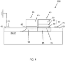
- FIG. 4 illustrates such an alternative embodiment, whereby a select device 80 is connected in series with the pinch-off ferroelectric memory FET 40 with no internal n+ junction 42 present, whereby the select device 80 may be a regular or n-type MOS stack comprising a doped gate dielectric layer (e.g. HfO 2 ) 60 resulting in an n-type MOS having anti-ferroelectric behavior.
- the select device 80 may comprise a select gate electrode 85 on top of a gate dielectric layer 60.
- the select device 80 may have a highly doped n+ junction as source region 41, whereby the select device 80 is provided on a p-type region 90.
- the pinch-off ferroelectric memory FET 40 comprises an n-type channel 35 provided in an n-type substrate 45.
- the p-type region 90 under the select device 80 may be provided by first providing a common n-type layer under the select device 80 and pinch-off ferroelectric memory FET 40, which thus would function as the n-type substrate 45 and thereafter defining a p-type region 90 by selective counterdoping.
- the p-type region 90 and n-type substrate 45, of respectively the select device 80 and pinch-off ferroelectric FET 40, may be provided on a common substrate, for example an oxide 47 or p-type substrate 46.
- the p-type region of the select device may act as a source region for the pinch-off ferroelectric FET and a highly doped n+ junction 43 may be provided as drain region.
- a source line electrode 72 and a bit line electrode 71 may in addition be provided on top of and in electrical contact with the source region 41 of the select transistor and the drain region 43 of the pinch off ferroelectric memory FET region, respectively.
- a split gate version of the device according to the embodiment illustrated in FIG. 4 is provided in FIG. 5 .
- a select gate electrode 91 is provided such that it overlaps and covers the gate electrode of the pinch-off ferroelectric FET 50 and acts as the gate electrode of the select transistor 80. As the select gate electrode 91 overlaps the gate electrode 50 of the pinch-off ferroelectric FET 40 a self-aligned memory cell is enabled.
- the select gate electrode 91 may be a second or top poly-Si gate acting as a word line (poly 2) and the gate electrode of the pinch-off ferroelectric FET 50 may be a first or lower poly-Si acting as the gate electrode (poly 1). For the avoidance of doubt, no floating gate construction is present in this embodiment.
- both electrodes 50, 91 are contacted, wherein poly 2 91 is contacted with the select gate or word line, and poly 1 50 is contacted with the plate line.
- the split gate version of the memory cell according to embodiments of the present invention advantageously eliminates the stacked gate issue of "over-erase", by isolating each memory cell from the bit line.
- the select transistors 80 differ from the ferroelectric pinch-off memory stacks 40 in that they are conventional MOSFETs.
- the select transistors 80 are switching elements rather than memory elements.
- the ferroelectric pinch-off memory cells 200 according to embodiments of the present invention, e.g. the at least one select device 80 and the ferroelectric memory FET 40, are illustrated as devices with planar geometries, which are formed by depositing semiconductor layers.
- embodiments of the present invention are not limited to planar geometries, as a person skilled in the art could easily translate the teaching of embodiments of the present invention in 3D structures, like for example using FinFET flow.
- FinFETs are 3D structures that rise above the substrate and resemble a fin, whereby the 'fins' form the source, channel and drain, effectively providing more volume than a planar transistor for the same area.
- the gate wraps around the fin, providing better control of the channel and allowing very little current to leak through the body when the device is in the 'off' state. This, in turn, enables the use of lower threshold voltages and results in better performance and power.
- the semiconductor substrate used in embodiments of the present invention is not specifically limited so long as it may be used for a semiconductor device.
- the substrate may be, for example, bulk substrates of elemental semiconductors of silicon, germanium and so on and compound semiconductors of silicon germanium, GaAs, InGaAs, ZnSe, GaN and so on.
- multilayer substrates such as an SOI (Silicon on Insulator) substrate, an SOS (Silicon on Sapphire) substrate or ceramics, glass or plastic substrate on top of which a semiconductor layer is processed.
- SOI Silicon on Insulator
- SOS Silicon on Sapphire
- ceramics glass or plastic substrate on top of which a semiconductor layer is processed.
- a silicon substrate or an SOI substrate on the surface of which a silicon layer is formed are preferred.
- the semiconductor substrate or the semiconductor layer may be single crystal (by, for example, epitaxial growth), polycrystalline or amorphous although there may be variations in the quantity of current flowing inside.
- isolation regions may be formed in the semiconductor substrate.
- active areas of the semiconductor devices of the present invention may be isolated from the underlying substrate.
- a corresponding isolation region 47 may be provided by a buried oxide (BOX) layer or other layers of dielectric material.
- BOX buried oxide
- shallow trench isolation (STI) areas may separate adjacent pairs of transistors. Formation of the buried oxide layer and areas of shallow trench isolation is well known in the art, and need not be explained in more detail here.
- a pinch-off ferroelectric memory FET 40 comprising an n-type channel 35 on an n-type substrate or in an n-type region 45.
- a n-type channel 35 is provided and a p-type wafer 46, then one may locally provide an n-type region 45 under the n-type channel in or on the p-type substrate, such as to enable provision of a pinch-off ferroelectric FET which modulates current in accumulation.
- pinch-off behavior can be accomplished by counterdoping a p-type well or substrate such that an n-type channel is generated in an n-type region, whereby the p-type is provided as a substrate under the select transistor and pinch-off ferroelectric FET.
- HfO 2 is typically used as gate dielectric in CMOS
- a ferroelectric layer as gate dielectric in the embedded memory cell would yield very compatible processing with the baseline CMOS. If then also a doped HfO 2 layer would be used for the CMOS (to enable anti-ferroelectric behavior) it would still be quite compatible, whereby on top of that a steeper subthreshold slope would be obtained for the CMOS.
- a pinch-off ferroelectric memory cell array may be provided, comprising a plurality of pinch-off ferroelectric memory cells 200, each comprising a ferroelectric memory FET 40 and a select device 80, e.g. a select transistor.
- Operations (erase, program and read) of the pinch-off memory cell array may be enabled by providing a plurality of word lines, source lines and bit lines as illustrated in FIG. 3.
- FIG. 3 illustrates a NOR array according to embodiments of the present invention.
- the memory cells can be arranged in rows and columns to form a memory array with source lines (SL1, SL2) coupled to a source of each non-volatile memory cell located in a given column; and a bit lines (B1, B2) coupled to a drain of each access or select transistor of the non-volatile memory cells in a given row.
- the drive electrode of the select device e.g. the gate of the select transistor, is connected to a wordline (WL1, WL2).
- the main function of the select device is to be able to cut the current in non-selected cells (since all memory transistors are always in the on state). More specifically, the select device is provided to cut the current of the non-selected cells on the same column to enable proper read out.
- an inhibit voltage is preferably applied to their bit lines to reduce the potential drop over the gate dielectric of the memory transistors (e.g. ferroelectric memory FETs), similar to the case of the 2T SRAM cell.
- the array of FIG. 3 also comprises plate lines (PL1, PL2) for driving one gate of the ferroelectric transistor of the non-volatile memory cell.
- the non-volatile memory cells can be located in a common n-region and/or a common n-doped layer.
- the cells may be mirrored around a symmetry axis S and around the source line, such that advantageously only half the typical contact area is needed per cell, resulting in a more compact device.
- the present invention relates to a method of manufacturing a non-volatile memory cell 200 according to embodiments of the present invention.
- the method comprises
- the pinch-off FeFET of the present invention may be fabricated on a p-type semiconductor wafer, for instance a p-type silicon wafer 46.
- a buried oxide layer (BOX) 47 may be provided in the wafer 46, as illustrated in FIG. 2 .
- an n-well may be provided at the location where the ferroelectric memory FET is to be provided.
- a ferroelectric gate stack 32 may be provided, in any suitable way.
- This gate stack 32 comprises at least one ferroelectric layer 32 and a gate electrode 50.
- a select transistor gate stack may be provided.
- This select transistor gate stack comprises a gate dielectric 60 and a select gate electrode 85.
- Both the gate stack 32 and the select transistor gate stack may then be used for defining the locations of n+ implants to be performed for forming source and drain regions 41, 42, 43 so as to form, together with the select transistor gate stack and the gate stack 32, the select transistor 80 and the ferroelectric memory FET 40, respectively.
- a replacement gate may be provided on the substrate 46.
- the drain and source regions may then be formed by using photolithography and implanting n+ dopants, like for example As+, in the source and drain regions aside the replacement gate, e.g. using ion beam implantation.
- the replacement gate may then be removed, after which an n- implant may be selectively provided in the p-type substrate under the ferroelectric stack, for example by counterdoping, where the replacement gate has been removed.
- Preferably providing said n- implant is performed using a relatively shallow implant similar to a threshold voltage adjust. This way, the n- implant is automatically aligned with the ferroelectric gate stack to be formed.
- the ferroelectric gate stack 32 is formed, comprising at least one ferroelectric layer 31 and optionally a dielectric layer in between the n- well and the stack of ferroelectric layers 31.
- a gate electrode 50 for instance a metal gate electrode, is provided on top of the ferroelectric layers, using methods known in the art.
- the channel is an n-type channel formed in the n- implant I, resulting in two accumulation levels.
Landscapes
- Engineering & Computer Science (AREA)
- Computer Hardware Design (AREA)
- Microelectronics & Electronic Packaging (AREA)
- Semiconductor Memories (AREA)
- Non-Volatile Memory (AREA)
Abstract
Description
- The present invention relates generally to a non-volatile ferroelectric pinch-off memory cell electrically connected in series with at least one select transistor and to methods of fabricating such non-volatile pinch-off ferroelectric memory cell electrically connected in series with at least one select transistor.
- Embedded non-volatile memory devices typically use floating gate structures or, in order to solve the scaling issue of floating gate memory devices, a discrete polysilicon-oxide-nitride-oxide-silicon (SONOS) structure to store electrostatic charges in the gate stack. Reading is then performed by sensing the current trough a channel which is modulated by this stored charge.
- However, putting charge in a floating gate or in a charge trapping layer (mostly the nitride in the SONOS structure which is non-conductive) take relatively high voltages (between 10-20V) Therefore, large charge pumping circuits have to be provided on-chip in order to generate these high voltages and large high voltage transistors are required to switch them In addition, writing will be much slower than reading. Moreover, the necessity of a charge pump requires a lot of additional processing steps making embedded non-volatile memory devices a very high-cost solution. For this reason, the use of embedded non-volatile memory devices has been limited to these applications where it is absolutely required (security, smart cards, automotive microcontrollers, etc.).
- Another non-volatile memory which has attracted great attention from the research community as a good candidate for both memory and switching applications is the ferroelectric field-effect transistor (FeFET) memory device. A state-of-the-art FeFET memory device resembles very much a metal-oxide-semiconductor FET (MOSFET); however, the gate oxide dielectric is replaced by a ferroelectric material for a FeFET memory device. By modulating the gate electrode, e.g. for n-MOS by applying a positive (Vcc) or negative voltage (-Vcc) -V inversion or accumulation, respectively, of the majority carriers will occur at the ferroelectric-semiconductor (channel) interface while writing/erasing and thereby switch the FeFET on ("1" state) or off ("0" state). As the gate voltage is released, the device remains in its state. These states correspond to the so-called remnant polarization states +Pr and -Pr, respectively. The bistable state of a ferroelectric can thus be programmed as binary information ("1" or "0"). This is due to the displacement of charges which is inherent to the crystal structure of the ferroelectric material and does not disappear in the absence of the electric field or gate voltage applied. This is why ferroelectric materials are very suitable for use in low-power non-volatile memories and advantageously require much lower program/erase voltages (typically +/-4V). In addition, these low program/erase voltages are obtained while keeping the same or even better functionality, like e.g. faster writing and erasing times. However, the introduction of the FeFET has been substantially delayed because of several reasons. Some of these reasons were solved when the ferroelectric phase in doped orthorhombic HfO2 was discovered, but FeFETs do suffer from a problem: the depolarization field which is due to the low permittivity of the silicon channel (about 12). As a result, in most cases the electric field over the materials in contact with the ferroelectric material can be different from zero even in the retention condition when no voltage is applied. As a consequence, there will also be an electric field over the ferroelectric material which is always opposite to the polarization (Gauss' law). That induced electric field will disadvantageously work against the polarization and hence depolarize the cell, which tends to slowly erase the cell.
- One way to remove this depolarization field is to use a pinch-off ferroelectric memory cell, e.g. a pinch-off ferroelectric FET. The pinch-off FET comprises a relatively highly doped n-type semiconductor channel on a n-type substrate, which will remain in accumulation even in the retention condition when no voltage is applied or in other words is always switched on (state "1"). According to embodiments of the present invention the channel length and/or doping used may be chosen such that the device can be pinch-off properly and provides the desired pinch-off voltage. However, when reading the cell state, i.e. the stored "1" or "0" data, from such a pinch-off ferroelectric FET, a negative gate bias (= read voltage) needs to be applied to the gate electrode in order to modulate the current and distinguish between a "1" and a "0" state. In a classical read-out scheme, this read voltage is placed between the two threshold voltage levels (programmed and erased), in order to have a current in one state and no current in the other one. In a pinch-off ferroelectric FET, however, such a scheme would correspond to a depleted state and an accumulation state. The depleted state would again introduce a depolarization field which again will cause the cell to lose its charge when reading it for a prolonged period of time.
- Therefor there is a need for novel and improved pinch-off ferroelectric memory cells.
- It is an object of embodiments of the present invention to provide good pinch-off ferroelectric memory cells and fabrication methods thereof. With good ferroelectric pinch-off memory cells is meant ferroelectric memory cells having good non-volatile properties, e.g. long retention times.
- The above objective is accomplished by a method and device according to embodiments of the present invention.
- In a first aspect, the present invention provides a non-volatile memory cell, comprising a pinch-off ferroelectric FET and at least one select device electrically connected in series to the pinch-off ferroelectric FET.
- It is an advantage of embodiments of the invention that the FeFET memory device electrically connected in series with a select transistor has excellent retention characteristics. The pinch-off ferroelectric FET and the at least one select device may for instance be planar devices or 3D devices (e.g. finFET).
- A pinch-off ferroelectric FET" is a depletion device, for instance an n-channel device that needs negative gate bias in order to be cut off, hence a device with a negative threshold voltage. As a result, contrary to common ferroelectric FETs, a pinch-off ferroelectric FET as referred to in embodiments of the present invention operates in two distinct accumulation modes, whereby the difference in current between both accumulation modes defines a window between the "0" and "1" state.
- It is an advantage of embodiments of the invention that by reading the ferroelectric pinch-off memory cells in accumulation there is no field across the ferroelectric layer in read mode, therefore avoiding read disturb due to the depolarization field.
- It is an advantage of embodiments of the invention that the appearance of a voltage drop over the stack is avoided whereby the depolarization field is brought back to zero ("is killed").
- It is an advantage of embodiments of the invention that the depolarization field is removed both under retention as well as under the read condition.
- It is an advantage of embodiments of the invention that the depolarization field is suppressed by design. Since a pinch-off FeFET is used in series with a select device, e.g. a conventional enhancement transistor, there is hardly any voltage drop over it and consequently also no field will appear across the ferroelectric layer, and as a result good retention is obtained.
- It is an advantage of embodiments of the invention that, since a pinch-off FeFET is used in series with a select device, e.g. a select transistor, the select transistor enables to cut off the current in non-selected cells in an array, which is required since all memory transistors are always in the on state.
- It is an advantage of embodiments of the invention that using a select device, e.g. a select transistor, in series with a pinch-off FeFET enables to select a bit by applying a select gate voltage. This way, the gate voltage on the memory cell can be kept at zero during read mode in order to have no depolarization field over the ferroelectric layer at any time.
- It is an advantage of embodiments of the invention that information leakage is restricted to a minimum.
- It is an advantage of embodiments of the invention that alternatives are provided for 2T floating gate or SONOS embedded memory non-volatile devices with lower program/erase voltages, faster programming times, and, moreover, without the typical drawbacks of depolarization fields in ferroelectric non-volatile memory devices.
- In a non-volatile memory cell according to embodiments of the present invention, the at least one select device may be at least one select transistor. This reduces complexity of the manufacturing process. It is an advantage of embodiments of the invention that no major changes are required to the materials bill nor to the process integration (e.g. no necessity of new tooling). As a result, embodiments of the present invention provide low cost concepts (compared to other embedded non-volatile devices) which are efficient and can be used as low power-consumption storage devices.
- It is an advantage of embodiments of the invention that ferroelectric memory cells are used, which are charge based, resulting in a device which is extremely low power having a small periphery.
- In a non-volatile memory cell according to embodiments of the present invention, the pinch-off ferroelectric FET may comprise a ferroelectric gate stack comprising at least one ferroelectric layer, with on top thereof a gate electrode; a source region and a drain region; and an n-type channel layer. The source region and drain region are electrically connected to the n-type channel layer. The pinch-off ferroelectric FET has a negative threshold voltage, and the at least one select transistor is an n-MOS gate stack comprising a select gate electrode. In a non-volatile memory cell according to embodiments of the present invention, the source and drain regions may be provided by highly doped n+ regions.
- Also the source and drain regions of the at least one select device may be provided by highly doped n+ regions. In particular embodiments, the drain region of the select device may act as a source region of the pinch-off ferroelectric FET. Alternatively, the source region of the select device may act as a drain region of the pinch-off ferroelectric FET.
- A non-volatile memory cell according to embodiments of the present invention may further comprise at least one dielectric layer between the at least one ferroelectric layer and the n-type channel and/or between the at least one ferroelectric layer and the gate electrode.
- In a non-volatile memory cell according to embodiments of the present invention, the n-type channel may be formed by counterdoping a p-type substrate provided under the pinch-off ferroelectric FET. Alternatively, the n-type channel layer may be provided in an n-type region under the pinch-off ferroelectric FET, whereby the n-type region may be provided on a p-type substrate or an insulator.
- In a non-volatile memory cell according to embodiments of the present invention, the at least select one select device and the pinch-off ferroelectric FET may be electrically connected in series between a bit line and an array ground. In embodiments of the present invention, the pinch-off ferroelectric FET may be positioned at the bit line side and the select device may be positioned at the side of the array ground. Alternatively, the pinch-off ferroelectric FET may be positioned at the side of the array ground and the select device may be positioned at the bit line side.
- Embodiments of the present invention advantageously may be used as a low-voltage alternative for non-volatile concepts on the market, like for example Electrically Erasable Programmable Read-Only Memory (EEPROM), resistive random-access memory (RRAM) and phase-change memory devices (PCM) and spin-transfer torque (STT) devices.
- In a second aspect, the present invention provides a non-volatile memory array, comprising a plurality of memory cells according to embodiments of the first aspect, logically arranged in rows and columns.
- In a further aspect, the present invention provides a method of operation of a non-volatile memory device according to embodiments of the first aspect, wherein data of the ferroelectric pinch-off memory gate stack in accumulation mode is read out without applying a voltage to the gate electrode of the ferroelectric pinch-off memory FET.
- Particular and preferred aspects of the invention are set out in the accompanying independent and dependent claims. Features from the dependent claims may be combined with features of the independent claims and with features of other dependent claims as appropriate and not merely as explicitly set out in the claims.
- These and other aspects of the invention will be apparent from and elucidated with reference to the embodiment(s) described hereinafter.
-
-
FIG. 1 schematically illustrates a cross-sectional view of a pinch-off FeFET electrically connected in series with a select transistor to form a ferroelectric pinch-off memory cell according to embodiments of the present invention. -
FIG. 2 schematically illustrates a cross-sectional view of an alternative embodiment of a pinch-off FeFET electrically connected in series with a select transistor to form a ferroelectric pinch-off memory cell according to embodiments of the present invention. -
FIG. 3 illustrates an equivalent circuit of a pinch-off FeFET cell array according to embodiments of the present invention -
FIG. 4 schematically illustrates a cross-sectional view of an alternative embodiment of a pinch-off FeFET electrically connected in series with a select transistor to form a ferroelectric pinch-off memory cell according to embodiments of the present invention. -
FIG. 5 schematically illustrates a split gate version of the embodiment illustrated inFIG. 4 . - The drawings are only schematic and are non-limiting. In the drawings, the size of some of the elements may be exaggerated and not drawn on scale for illustrative purposes.
- Any reference signs in the claims shall not be construed as limiting the scope.
- In the different drawings, the same reference signs refer to the same or analogous elements.
- The present invention will be described with respect to particular embodiments and with reference to certain drawings but the invention is not limited thereto but only by the claims. The drawings described are only schematic and are non-limiting. In the drawings, the size of some of the elements may be exaggerated and not drawn on scale for illustrative purposes. The dimensions and the relative dimensions do not correspond to actual reductions to practice of the invention.
- The terms first, second and the like in the description and in the claims, are used for distinguishing between similar elements and not necessarily for describing a sequence, either temporally, spatially, in ranking or in any other manner. It is to be understood that the terms so used are interchangeable under appropriate circumstances and that the embodiments of the invention described herein are capable of operation in other sequences than described or illustrated herein.
- Moreover, the terms top, under and the like in the description and the claims are used for descriptive purposes and not necessarily for describing relative positions. It is to be understood that the terms so used are interchangeable under appropriate circumstances and that the embodiments of the invention described herein are capable of operation in other orientations than described or illustrated herein.
- It is to be noticed that the term "comprising", used in the claims, should not be interpreted as being restricted to the means listed thereafter; it does not exclude other elements or steps. It is thus to be interpreted as specifying the presence of the stated features, integers, steps or components as referred to, but does not preclude the presence or addition of one or more other features, integers, steps or components, or groups thereof. Thus, the scope of the expression "a device comprising means A and B" should not be limited to devices consisting only of components A and B. It means that with respect to the present invention, the only relevant components of the device are A and B.
- Reference throughout this specification to "one embodiment" or "an embodiment" means that a particular feature, structure or characteristic described in connection with the embodiment is included in at least one embodiment of the present invention. Thus, appearances of the phrases "in one embodiment" or "in an embodiment" in various places throughout this specification are not necessarily all referring to the same embodiment, but may. Furthermore, the particular features, structures or characteristics may be combined in any suitable manner, as would be apparent to one of ordinary skill in the art from this invention, in one or more embodiments.
- Similarly it should be appreciated that in the description of exemplary embodiments of the invention, various features of the invention are sometimes grouped together in a single embodiment, figure, or description thereof for the purpose of streamlining the invention and aiding in the understanding of one or more of the various inventive aspects. This method of invention, however, is not to be interpreted as reflecting an intention that the claimed invention requires more features than are expressly recited in each claim. Rather, as the following claims reflect, inventive aspects lie in less than all features of a single foregoing disclosed embodiment. Thus, the claims following the detailed description are hereby expressly incorporated into this detailed description, with each claim standing on its own as a separate embodiment of this invention.
- Furthermore, while some embodiments described herein include some but not other features included in other embodiments, combinations of features of different embodiments are meant to be within the scope of the invention, and form different embodiments, as would be understood by those in the art. For example, in the following claims, any of the claimed embodiments can be used in any combination.
- In the description provided herein, numerous specific details are set forth. However, it is understood that embodiments of the invention may be practiced without these specific details. In other instances, well-known methods, structures and techniques have not been shown in detail in order not to obscure an understanding of this description.
- Where in embodiments of the present invention reference is made to "a pinch-off ferroelectric FET", reference is made to a depletion device, like for example an n-channel ferroelectric FET of which the n-type channel is provided in an n-type substrate (which may be an n-type layer on, typically, p-type substrate, or on an insulator like an oxide, e.g. in the case of SOI technology), whereby a ferroelectric gate dielectric may be provided on top of the n-channel. When referring to a depletion device one may refer to an n-channel device that needs negative gate bias in order to be cut off, hence a device with a negative threshold voltage. As a result, contrary to common ferroelectric FETs, a pinch-off ferroelectric FET as referred to in embodiments of the present invention operates in two distinct accumulation modes, whereby the difference in current between both accumulation modes defines a window between the "0" and "1" state. In embodiments of the present invention a pinch-off FeFET is preferably biased between the edge of the accumulation state (e.g. close to depletion state) and the 'deep accumulation' state in order to have an appreciable window. For avoidance of doubt it is clarified that it is not the intention of the present invention to use ferroelectric FETs in the actual pinched-off mode..
- Where in embodiments of the present invention reference is made to a "substrate" reference is made to an object or layer or stack of layers onto which a layer of interest is applied.
- Embodiments of the present invention provide an array of memory cells logically organized in rows and columns. The terms "horizontal" and "vertical" (related to the terms "row" and "column" respectively) may be used to provide a co-ordinate system, for ease of explanation only. They do not need to, but may, refer to an actual physical direction of the device. The terms "column" and "row" may be used to describe sets of array elements which are linked together. The linking of the memory cells in the array can be in the form of a Cartesian array of rows and columns; however, the present invention is not limited thereto. As will be understood by those skilled in the art, columns and rows can be easily interchanged and it is intended in this disclosure that these terms be interchangeable. Also, non-Cartesian arrays may be constructed and are included within the scope of the invention. Accordingly, the terms "row" and "column" should be interpreted widely. To facilitate in this wide interpretation, the claims refer to memory cells being logically organized in rows and columns. By this is meant that sets of memory cells are linked together in a topologically linear intersecting manner; however, that the physical or topographical arrangement need not be so. For example, the rows may be circles and the columns radii of these circles and the circles and radii are described in this invention as "logically organized" rows and columns. Also, specific names of the various lines, e.g. select line, bit line, word line, are intended to be generic names used to facilitate the explanation and to refer to a particular function and this specific choice of words is not intended to in any way limit the invention. It should be understood that all these terms are used only to facilitate a better understanding of the specific structure being described, and are in no way intended to limit the invention.
- A ferroelectric (FeFET) memory device is a memory device which makes use of a ferroelectric layer, such as for instance lead zirconate titanate (PZT), for storing data. By applying an external field, e.g. a gate voltage, to the gate electrode, accumulation or depletion of the majority carries will occur at the interface between the ferroelectric layer and the semiconducting channel. Upon applying a gate voltage, polarization of the ferroelectric layer will occur and the device will turn on ("1" state) or off ("0" state). As the gate voltage is released, the device retains its state. These states correspond to the so-called remnant polarization +Pr and -Pr, respectively. The bistable state of a ferroelectric can thus be programmed as binary information ("1" or "0"). This is due to the displacement of charges which is inherent to the crystal structure of the ferroelectric material and does not disappear in the absence of the electric field or gate voltage applied. This is why ferroelectric materials are very suitable for use in low-power non-volatile memories. In addition, the direction of the polarization P can be reversed or reoriented by applying an appropriate electric field (gate voltage).
- It is known that a prior art ferroelectric memory device does not have the desired long-term non-volatility. The information leaking away is due to a depolarization field being present, which is finite due to the finite permittivity of the semiconducting channel. Since Si has a low permittivity of about 12, and most ferroelectric materials have high permittivity values, this leakage situation is bound to occur in any ferroelectric memory device using silicon as a channel material. This is the main reason why ferroelectric memory devices have not made it into the market place so far.
- Compared to conventional inversion mode FeFETs, the use of n-doped devices working in accumulation mode, or a so called pinch-off ferroelectric (FeFET) memory device, advantageously can remove this depolarization field since the channel may be a relatively highly doped n-type semiconducting channel which remains in accumulation during zero voltage or retention conditions. However, when reading the pinch-off FeFET cell, a negative gate bias is typically applied in order to modulate the current and distinguish between a "1" state and a "0" state. In a classical read-out scheme, this read voltage is placed between the two threshold voltage levels (Vt) (programmed and erased), in order to have a current in one state and no current in the other one. In a pinch-off FeFET, such a scheme would however correspond to a depleted state and an accumulation state respectively. Unfortunately, the depleted state (which would be enabled when applying the highest threshold voltage (Vt) which is known as the pinch-off voltage (Vpo)) would again introduce a depolarization field which again will cause the cell to lose its charge and thus its non-volatile behavior when reading it for a prolonged period of time.
- To solve this problem, in a first aspect, embodiments of the present invention provide a ferroelectric pinch-off memory stack electrically connected in series to a select device such as a select transistor, as schematically illustrated for different embodiments in
FIG. 1 and FIG. 2 . It is an advantage of embodiments of the present invention that by putting a select device, e.g. a select transistor, electrically in series with a pinch-off ferroelectric memory cell, the ferroelectric pinch-off memory cell is kept conductive. In addition, by reading the ferroelectric pinch-off memory cell at zero gate voltage one enables that the ferroelectric pinch-off memory cell is never in depletion and that it will not lose its charge of non-volatile behavior. According to embodiments of the present invention the select device, e.g. select transistor, and the ferroelectric pinch-off memory element are electrically connected in series between a bit line and an array ground, whereby the ferroelectric pinch-off memory cell may be positioned at the bit line side or source line side. According to particular embodiments, the select device may be positioned at the bit line side in order to disconnect the ferroelectric pinch-off memory element from the bit line voltage. Preferably, a drive electrode of the select device, e.g. the gate of the select transistor, is connected to a wordline. The presence of the select device is required in embodiments of the present invention since the gate of the memory element can no longer be used to select a particular bit on a wordline. In addition, by using a select device, electrically connected in series with a ferroelectric pinch-off memory cell, the select device advantageously enables to cut the current in non-selected cells, since the ferroelectric pinch-off memory element is always in the on state. The select device moreover may have a second function: to select the bit by applying a select gate voltage. This way, the gate voltage on the cell can be kept at 0 V during read, in order to have no depolarization field over the ferroelectric layer at any time. - According to embodiments of the present invention, when the state of the pinch-off ferroelectric memory cell is to be read, the select transistor is turned on via a voltage (Vcc) applied to wordline, and a read voltage (Vcc) is applied to bit line to determine the conductive state of ferroelectric pinch-off memory cell. And thus when reading, advantageously there is zero voltage applied on the ferroelectric pinch-off memory element and there is no depolarization field over the ferroelectric layer and the gate of the ferroelectric pinch-off memory element is no longer used to select a particular bit on a wordline. According to embodiments of the present invention the signal of the sense amplifier may be a current difference between a programmed and erased state of a ferroelectric pinch-off memory cell in accumulation mode, which is indicative of the charge that was released by the ferroelectric pinch-off memory cell. Therefore, according to embodiments of the present invention, the difference between these two on states defines the bit of the ferroelectric pinch-off memory cell. Advantageously, by using the difference, the field across the stack of the memory cell is removed while reading therefore avoiding read disturb due to a depolarization field. The memory cell is programmed or erased by applying an appropriate voltage between memory element control gate and bit line, with the select device turned off, e.g. zero volt being applied to the gate of the select transistor. Table I provides an operating table with typical values of operating voltages for programing (write), erasing and reading a ferroelectric pinch-off memory element electrically connected in series with a select transistor according to embodiments of the present invention.
Table I: Operating table of a ferroelectric pinch-off memory cell connected in series with a select transistor according to embodiments of the present invention. Operating table Select gate Cell gate Source Drain Write select /deselect 0 4V/4V 0 0/4V Page erase 0 -4V 0 0 Read Vcc 0 0 Vcc - Since sense amplifiers typically flip based on absolute and not based on relative current levels, this does not necessarily imply a lower read speed and the cell with presented read out scheme in Table I can also be used in read intensive NOR applications without any risk for read disturb.
- In an exemplary embodiment, like for example illustrated in
FIGS. 1 and 2 , a ferroelectric pinch-off memory FET 40 comprises a source region, a drain region and a ferroelectric gate stack over an n-type channel layer, whereby the n-type channel 35 layer may be provided in an n-type substrate 45. The n-type substrate may be generated in a p-type substrate by counterdoping or alternatively when SOI technology is preferred the n-type substrate is provided on an insulating layer like anoxide 47, as illustrated inFIG. 2 . In embodiments, as illustrated inFIG. 1 , where an n-type channel in an n-type region is provided in a p-type substrate by for example counterdoping, the p-type substrate also acts as a substrate of the select device, resulting in an n-type MOS transistor as select device. The source region and drain region are electrically coupled to either side of the n-type channel layer. At least one dielectric layer may be present between the ferroelectric gate region and the n-type channel and/or between the ferroelectric gate region and a gate electrode. - In a particular embodiment, a
non-volatile memory cell 200 comprises a pinch offferroelectric memory FET 40 connected in series with aselect device 80. Theferroelectric memory FET 40 comprises agate electrode 50 such as a metal gate electrode, e.g. a few nm of TiN, on top of aferroelectric gate stack 32. Theferroelectric gate stack 32 comprises one or moreferroelectric layers 31, for instance a 5 nm Al-doped HfO2 in orthorhombic phase; and optionally at least onedielectric layer 30, for instance a SiO2 layer or a few nm's of Hf-Al-O. Theferroelectric gate stack 32 is provided on top of an n-typesemiconductor channel layer 35. The n-typesemiconductor channel layer 35 is configured such that the pinch offferroelectric memory FET 40 needs negative gate bias in order to be cut off, hence a pinch offferroelectric memory FET 40 with a negative threshold voltage. The latter can be accomplished by counterdoping with an n-type or donor element (e.g. As or P) in a conventional n-type MOS process. Thegate electrode 50 is provided on top of theferroelectric layers 31 and the n-type semiconductor channel 35 is provided on or in an n-type substrate 45, for instance an n-implant in a p-type substrate 46, as illustrated inFIG. 1 . Highly doped n+junctions are provided as source and drain regions, for example as source and drainregions select device 80 or as source and drainregion type semiconductor channel 35, whereby the drain region of the select device acts as a source region of the a pinch offferroelectric memory FET 40. Asource line electrode 72 and abit line electrode 71 may in addition be provided on top of and in electrical contact with thesource region 41 of the select transistor and thedrain region 43 of the pinch offferroelectric memory FET 40, respectively. Thedrain electrode 71 functions as or is electrically connected to a bit line when programing or erasing the memory cell. As illustrated inFIGS. 1 and 2 , sinceregion 42 is an internal node, there is no need to electrically contact this region. In alternative embodiments, for example in conventional NOR arrays, area savings may be realized by only contacting thebit line electrode 71 while thesource line electrode 72 is a buried diffusion layer (like for example illustrated inFIG. 3 further on). - The at least one
select device 80, for instance in the embodiment illustrated a select transistor, may be an n-type MOS stack comprising aselect gate electrode 85 on top of agate dielectric layer 60. Also theselect device 80 may have highly doped n+ junctions as source and drainregions ferroelectric memory FET 40 is an electronic component which is separate from theselect transistor 80. In embodiments of the present invention, thedrain region 42 of theselect transistor 80 may coincide with thesource region 42 of theferroelectric memory FET 40. Alternatively, in embodiments which are not illustrated, the source region of theselect transistor 80 may coincide with the drain region of theferroelectric memory FET 40. - In alternative embodiments the highly doped
n+ junction 42 acting as drain region for the select device and as source region for the pinch-off memory device may be removed resulting in a more compact device.FIG. 4 illustrates such an alternative embodiment, whereby aselect device 80 is connected in series with the pinch-offferroelectric memory FET 40 with nointernal n+ junction 42 present, whereby theselect device 80 may be a regular or n-type MOS stack comprising a doped gate dielectric layer (e.g. HfO2) 60 resulting in an n-type MOS having anti-ferroelectric behavior. Theselect device 80 may comprise aselect gate electrode 85 on top of agate dielectric layer 60. Theselect device 80 may have a highly doped n+ junction assource region 41, whereby theselect device 80 is provided on a p-type region 90. The pinch-offferroelectric memory FET 40 comprises an n-type channel 35 provided in an n-type substrate 45. The p-type region 90 under theselect device 80 may be provided by first providing a common n-type layer under theselect device 80 and pinch-offferroelectric memory FET 40, which thus would function as the n-type substrate 45 and thereafter defining a p-type region 90 by selective counterdoping. - The p-
type region 90 and n-type substrate 45, of respectively theselect device 80 and pinch-offferroelectric FET 40, may be provided on a common substrate, for example anoxide 47 or p-type substrate 46. The p-type region of the select device may act as a source region for the pinch-off ferroelectric FET and a highly dopedn+ junction 43 may be provided as drain region. Asource line electrode 72 and abit line electrode 71 may in addition be provided on top of and in electrical contact with thesource region 41 of the select transistor and thedrain region 43 of the pinch off ferroelectric memory FET region, respectively. In yet alternative embodiments, a split gate version of the device according to the embodiment illustrated inFIG. 4 is provided inFIG. 5 . Aselect gate electrode 91 is provided such that it overlaps and covers the gate electrode of the pinch-offferroelectric FET 50 and acts as the gate electrode of theselect transistor 80. As theselect gate electrode 91 overlaps thegate electrode 50 of the pinch-off ferroelectric FET 40 a self-aligned memory cell is enabled. Theselect gate electrode 91 may be a second or top poly-Si gate acting as a word line (poly 2) and the gate electrode of the pinch-offferroelectric FET 50 may be a first or lower poly-Si acting as the gate electrode (poly 1). For the avoidance of doubt, no floating gate construction is present in this embodiment. As a result, in this embodiment, bothelectrodes - In embodiments of the present invention the
select transistors 80 differ from the ferroelectric pinch-off memory stacks 40 in that they are conventional MOSFETs. Theselect transistors 80 are switching elements rather than memory elements. The ferroelectric pinch-off memory cells 200 according to embodiments of the present invention, e.g. the at least oneselect device 80 and theferroelectric memory FET 40, are illustrated as devices with planar geometries, which are formed by depositing semiconductor layers. However, embodiments of the present invention are not limited to planar geometries, as a person skilled in the art could easily translate the teaching of embodiments of the present invention in 3D structures, like for example using FinFET flow. FinFETs are 3D structures that rise above the substrate and resemble a fin, whereby the 'fins' form the source, channel and drain, effectively providing more volume than a planar transistor for the same area. The gate wraps around the fin, providing better control of the channel and allowing very little current to leak through the body when the device is in the 'off' state. This, in turn, enables the use of lower threshold voltages and results in better performance and power. - The semiconductor substrate used in embodiments of the present invention is not specifically limited so long as it may be used for a semiconductor device. The substrate may be, for example, bulk substrates of elemental semiconductors of silicon, germanium and so on and compound semiconductors of silicon germanium, GaAs, InGaAs, ZnSe, GaN and so on. Moreover, it is acceptable to employ multilayer substrates such as an SOI (Silicon on Insulator) substrate, an SOS (Silicon on Sapphire) substrate or ceramics, glass or plastic substrate on top of which a semiconductor layer is processed. Among others, a silicon substrate or an SOI substrate on the surface of which a silicon layer is formed are preferred. The semiconductor substrate or the semiconductor layer may be single crystal (by, for example, epitaxial growth), polycrystalline or amorphous although there may be variations in the quantity of current flowing inside.
- In embodiments of the present invention, optionally, isolation regions may be formed in the semiconductor substrate. In one embodiment, as illustrated in
FIG. 2 , active areas of the semiconductor devices of the present invention may be isolated from the underlying substrate. Acorresponding isolation region 47 may be provided by a buried oxide (BOX) layer or other layers of dielectric material. In the same or alternative embodiments (not illustrated in the drawings), shallow trench isolation (STI) areas may separate adjacent pairs of transistors. Formation of the buried oxide layer and areas of shallow trench isolation is well known in the art, and need not be explained in more detail here. - It is, however, essential that materials used as semiconductor substrate enable the formation of a pinch-off
ferroelectric memory FET 40 comprising an n-type channel 35 on an n-type substrate or in an n-type region 45. In an exemplary embodiment, when a n-type channel 35 is provided and a p-type wafer 46, then one may locally provide an n-type region 45 under the n-type channel in or on the p-type substrate, such as to enable provision of a pinch-off ferroelectric FET which modulates current in accumulation. In embodiments of the present invention such pinch-off behavior can be accomplished by counterdoping a p-type well or substrate such that an n-type channel is generated in an n-type region, whereby the p-type is provided as a substrate under the select transistor and pinch-off ferroelectric FET. - Since HfO2 is typically used as gate dielectric in CMOS, a ferroelectric layer as gate dielectric in the embedded memory cell would yield very compatible processing with the baseline CMOS. If then also a doped HfO2 layer would be used for the CMOS (to enable anti-ferroelectric behavior) it would still be quite compatible, whereby on top of that a steeper subthreshold slope would be obtained for the CMOS.
- According to embodiments of the present invention, a pinch-off ferroelectric memory cell array may be provided, comprising a plurality of pinch-off
ferroelectric memory cells 200, each comprising aferroelectric memory FET 40 and aselect device 80, e.g. a select transistor. Operations (erase, program and read) of the pinch-off memory cell array may be enabled by providing a plurality of word lines, source lines and bit lines as illustrated inFIG. 3. FIG. 3 illustrates a NOR array according to embodiments of the present invention. The memory cells can be arranged in rows and columns to form a memory array with source lines (SL1, SL2) coupled to a source of each non-volatile memory cell located in a given column; and a bit lines (B1, B2) coupled to a drain of each access or select transistor of the non-volatile memory cells in a given row. The drive electrode of the select device, e.g. the gate of the select transistor, is connected to a wordline (WL1, WL2). The main function of the select device is to be able to cut the current in non-selected cells (since all memory transistors are always in the on state). More specifically, the select device is provided to cut the current of the non-selected cells on the same column to enable proper read out. In order not to program or erase these non-selected cells on the same row, an inhibit voltage is preferably applied to their bit lines to reduce the potential drop over the gate dielectric of the memory transistors (e.g. ferroelectric memory FETs), similar to the case of the 2T SRAM cell. The array ofFIG. 3 also comprises plate lines (PL1, PL2) for driving one gate of the ferroelectric transistor of the non-volatile memory cell. - The non-volatile memory cells can be located in a common n-region and/or a common n-doped layer. In embodiments of the present invention the cells may be mirrored around a symmetry axis S and around the source line, such that advantageously only half the typical contact area is needed per cell, resulting in a more compact device.
- In a further aspect, the present invention relates to a method of manufacturing a
non-volatile memory cell 200 according to embodiments of the present invention. The method comprises - providing a pinch-off
ferroelectric memory FET 40; and - providing at least a select device, for instance a
select transistor 80; - The materials used in the method according to embodiments of the present invention may be as set out above, in embodiments of earlier-described aspects of the invention.
- In an exemplary embodiment the pinch-off FeFET of the present invention may be fabricated on a p-type semiconductor wafer, for instance a p-
type silicon wafer 46. As complete isolation of the active areas from theunderlying silicon substrate 46 may be preferred, a buried oxide layer (BOX) 47 may be provided in thewafer 46, as illustrated inFIG. 2 . - If the
substrate 46 is a p-type substrate, an n-well may be provided at the location where the ferroelectric memory FET is to be provided. Above the n-well, aferroelectric gate stack 32 may be provided, in any suitable way. Thisgate stack 32 comprises at least oneferroelectric layer 32 and agate electrode 50. Besides theferroelectric gate stack 32, also a select transistor gate stack may be provided. This select transistor gate stack comprises agate dielectric 60 and aselect gate electrode 85. Both thegate stack 32 and the select transistor gate stack may then be used for defining the locations of n+ implants to be performed for forming source and drainregions gate stack 32, theselect transistor 80 and theferroelectric memory FET 40, respectively. - In alternative embodiments where the
substrate 46 is a p-type substrate, first a replacement gate may be provided on thesubstrate 46. The drain and source regions may then be formed by using photolithography and implanting n+ dopants, like for example As+, in the source and drain regions aside the replacement gate, e.g. using ion beam implantation. The replacement gate may then be removed, after which an n- implant may be selectively provided in the p-type substrate under the ferroelectric stack, for example by counterdoping, where the replacement gate has been removed. Preferably providing said n- implant is performed using a relatively shallow implant similar to a threshold voltage adjust. This way, the n- implant is automatically aligned with the ferroelectric gate stack to be formed. On top of the n- implant, theferroelectric gate stack 32 is formed, comprising at least oneferroelectric layer 31 and optionally a dielectric layer in between the n- well and the stack offerroelectric layers 31. Agate electrode 50, for instance a metal gate electrode, is provided on top of the ferroelectric layers, using methods known in the art. - It is to be noted that since the
ferroelectric memory FETs 40 are accumulation-mode devices, the channel is an n-type channel formed in the n- implant I, resulting in two accumulation levels. - While the basic processes are described above with specific reference to the fabrication of memory devices or arrays according to the present invention, there are several optional steps known to those skilled in the art that may be used. In addition, although the basic processes described above are utilized in the fabrication, those skilled in the art will recognize the order in which the basic processes are performed may be varied to achieve the desired structures.
Claims (14)
- A non-volatile memory cell (200), the cell (200) comprising a pinch-off ferroelectric FET (40) and at least one select device (80), said at least one select device (80) being electrically connected in series to the pinch-off ferroelectric FET (40).
- The non-volatile memory cell (200), wherein the at least one select device (80) is at least one select transistor.
- The non-volatile memory cell (200) according to any of the previous claims, wherein the pinch-off ferroelectric FET (40) comprises:• a ferroelectric gate stack (32) comprising at least one ferroelectric layer, with on top thereof a gate electrode (50);• a source region (42) and a drain region (43);• an n-type channel layer (35)wherein the source region (42) and drain region (43) are electrically connected to the n-type channel layer (35); and
wherein the pinch-off ferroelectric FET (40) has a negative threshold voltage; and wherein the at least one select transistor (80) is an n-MOS gate stack comprising a select gate electrode (85). - The non-volatile memory cell (200) according to claim 3, wherein the source (42) and drain (43) regions are provided by highly doped n+ regions.
- The non-volatile memory cell (200) according to any of claims 3 or 4, wherein the at least one select device (80) comprises source (41) and drain (42) regions, which are provided by highly doped n+ regions.
- The non-volatile memory cell (200) according to any one of claims 3 to 5, wherein the drain region (42) of the select device (80) acts as a source region (42) of the pinch-off ferroelectric FET (40).
- The non-volatile memory cell (200) according to any one of claims 3 to 6, further comprising at least one dielectric layer (30), wherein the at least one dielectric layer (30) is between the at least one ferroelectric layer (31) and the n-type channel (35) and/or between the at least one ferroelectric layer (31) and the gate electrode (50).
- The non-volatile memory cell (200) according to any one claims 3 to 7, wherein the n-type channel is formed by counterdoping a p-type substrate provided under the pinch-off ferroelectric FET (40).
- The non-volatile memory cell (200) according to any of claims 3 or 7, wherein the n-type channel layer (35) is provided in an n-type region (45) under the pinch-off ferroelectric FET, whereby the n-type region (45) is provided on a p-type substrate (46) or an insulator (47).
- The non-volatile memory cell (200) according to any of previous claims, wherein the at least select one select device (80) and the pinch-off ferroelectric FET (40) are electrically connected in series between a bit line (100) and an array ground.
- The non-volatile memory cell (200) according to claim 10, wherein the pinch-off ferroelectric FET (40) is positioned at the bit line side and the select device (80) is positioned at the side of the array ground.
- The non-volatile memory cell (200) according to claim 10, wherein the pinch-off ferroelectric FET (40) is positioned at the side of the array ground and the select device (80) is positioned at the bit line side.
- A non-volatile memory array, comprising a plurality of memory cells (200) according to any of the previous claims, logically arranged in rows and columns.
- A method of operation of a non-volatile memory device (200) according to any of claims 1 to 12, wherein data of the ferroelectric pinch-off memory gate stack (40) in accumulation mode is read out without applying a voltage to the gate electrode (50) of the ferroelectric pinch-off memory FET (40).
Applications Claiming Priority (1)
| Application Number | Priority Date | Filing Date | Title |
|---|---|---|---|
| EP15201648 | 2015-12-21 |
Publications (2)
| Publication Number | Publication Date |
|---|---|
| EP3185281A1 true EP3185281A1 (en) | 2017-06-28 |
| EP3185281B1 EP3185281B1 (en) | 2026-03-18 |
Family
ID=55024883
Family Applications (1)
| Application Number | Title | Priority Date | Filing Date |
|---|---|---|---|
| EP16205702.0A Active EP3185281B1 (en) | 2015-12-21 | 2016-12-21 | Ferroelectric pinch-off memory cell |
Country Status (2)
| Country | Link |
|---|---|
| US (1) | US10090036B2 (en) |
| EP (1) | EP3185281B1 (en) |
Cited By (1)
| Publication number | Priority date | Publication date | Assignee | Title |
|---|---|---|---|---|
| FR3082658A1 (en) * | 2018-06-15 | 2019-12-20 | Stmicroelectronics (Crolles 2) Sas | TRANSISTOR FEFET |
Families Citing this family (32)
| Publication number | Priority date | Publication date | Assignee | Title |
|---|---|---|---|---|
| US11120884B2 (en) | 2015-09-30 | 2021-09-14 | Sunrise Memory Corporation | Implementing logic function and generating analog signals using NOR memory strings |
| WO2019066948A1 (en) * | 2017-09-29 | 2019-04-04 | Intel Corporation | Double-gated ferroelectric field-effect transistor |
| US10276697B1 (en) * | 2017-10-27 | 2019-04-30 | Taiwan Semiconductor Manufacturing Co., Ltd. | Negative capacitance FET with improved reliability performance |
| US10210921B1 (en) * | 2018-02-23 | 2019-02-19 | Seoul National University RDB foundation | Non-volatile ferroelectric memory device and method of driving the same |
| US10734398B2 (en) | 2018-08-29 | 2020-08-04 | Taiwan Semiconductor Manufacturing Co., Ltd. | Flash memory structure with enhanced floating gate |
| DE102019104255B4 (en) | 2018-08-29 | 2023-03-16 | Taiwan Semiconductor Manufacturing Co. Ltd. | Memory structure with FeRAM device and method for its production as well as an integrated chip with a first FeRAM cell and a second FeRAM cell |
| US10930333B2 (en) * | 2018-08-29 | 2021-02-23 | Taiwan Semiconductor Manufacturing Co., Ltd. | Embedded ferroelectric memory cell |
| DE102019117751A1 (en) | 2018-08-29 | 2020-03-05 | Taiwan Semiconductor Manufacturing Co. Ltd. | FLASH MEMORY STRUCTURE WITH IMPROVED FLOATING GATE |
| US10727251B2 (en) * | 2018-12-03 | 2020-07-28 | Globalfoundries Inc. | Rounded shaped transistors for memory devices |
| US10923502B2 (en) | 2019-01-16 | 2021-02-16 | Sandisk Technologies Llc | Three-dimensional ferroelectric memory devices including a backside gate electrode and methods of making same |
| US10879269B1 (en) | 2019-06-27 | 2020-12-29 | Sandisk Technologies Llc | Ferroelectric memory device containing a series connected select gate transistor and method of forming the same |
| US11031490B2 (en) * | 2019-06-27 | 2021-06-08 | Taiwan Semiconductor Manufacturing Co., Ltd | Fabrication of field effect transistors with ferroelectric materials |
| EP3895213B1 (en) * | 2019-06-27 | 2026-03-18 | Sandisk Technologies, Inc. | Ferroelectric memory device containing a series connected select gate transistor and method of forming the same |
| US10916287B2 (en) * | 2019-06-27 | 2021-02-09 | Sandisk Technologies Llc | Ferroelectric memory device containing a series connected select gate transistor and method of forming the same |
| US10978485B2 (en) * | 2019-09-09 | 2021-04-13 | Macronix International Co., Ltd. | Vertical-channel ferroelectric flash memory |
| CN112466892B (en) * | 2019-09-09 | 2024-12-20 | 旺宏电子股份有限公司 | Memory, integrated circuit memory, and method for manufacturing memory |
| US11527646B2 (en) | 2019-09-24 | 2022-12-13 | Samsung Electronics Co., Ltd. | Domain switching devices and methods of manufacturing the same |
| US11139315B2 (en) * | 2019-10-31 | 2021-10-05 | Qualcomm Incorporated | Ferroelectric transistor |
| US11515309B2 (en) | 2019-12-19 | 2022-11-29 | Sunrise Memory Corporation | Process for preparing a channel region of a thin-film transistor in a 3-dimensional thin-film transistor array |
| US12550382B2 (en) * | 2020-01-22 | 2026-02-10 | Sunrise Memory Corporation | Thin-film storage transistor with ferroelectric storage layer |
| US12256547B2 (en) | 2020-01-22 | 2025-03-18 | Sunrise Memory Corporation | Silicon oxide nitride tunnel dielectric for a storage transistor in a 3-dimensional NOR memory string array |
| TWI767512B (en) | 2020-01-22 | 2022-06-11 | 美商森恩萊斯記憶體公司 | Cool electron erasing in thin-film storage transistors |
| WO2021159028A1 (en) | 2020-02-07 | 2021-08-12 | Sunrise Memory Corporation | High capacity memory circuit with low effective latency |
| DE102021105038A1 (en) * | 2020-05-29 | 2021-12-02 | Taiwan Semiconductor Manufacturing Co., Ltd. | MULTI-BIT STORAGE DEVICE AND METHOD OF OPERATING THE SAME |
| US11430510B2 (en) | 2020-12-11 | 2022-08-30 | International Business Machines Corporation | Multi-level ferroelectric field-effect transistor devices |
| TWI915580B (en) | 2021-07-16 | 2026-02-21 | 美商日升存儲公司 | 3-dimensional memory string array of thin-film ferroelectric transistors |
| JP7706012B2 (en) | 2021-09-03 | 2025-07-10 | サンライズ メモリー コーポレイション | 3D NOR MEMORY STRING ARRAY OF THIN FILM FERROELECTRIC TRANSISTORS |
| US12402319B2 (en) | 2021-09-14 | 2025-08-26 | Sunrise Memory Corporation | Three-dimensional memory string array of thin-film ferroelectric transistors formed with an oxide semiconductor channel |
| EP4203066A1 (en) * | 2021-12-21 | 2023-06-28 | IMEC vzw | Split gate ferrofet |
| US11990171B2 (en) * | 2022-02-15 | 2024-05-21 | Globalfoundries U.S. Inc. | Threshold voltage-programmable field effect transistor-based memory cells and look-up table implemented using the memory cells |
| KR20240068207A (en) * | 2022-11-10 | 2024-05-17 | 삼성전자주식회사 | Field effect transistor, capacitor, and electronic apparatus including domain-controlled ferroelectric material |
| US12324357B2 (en) * | 2023-10-13 | 2025-06-03 | Nanjing University | Voltage-controlled three-terminal magnon transistor, and control and preparation method thereof |
Citations (3)
| Publication number | Priority date | Publication date | Assignee | Title |
|---|---|---|---|---|
| WO1999019878A1 (en) * | 1997-10-14 | 1999-04-22 | Yale University | A ferroelectric dynamic random access memory |
| EP0923135A1 (en) * | 1997-12-09 | 1999-06-16 | Fujitsu Limited | Ferroelectric memory device |
| US20070228432A1 (en) * | 2006-01-03 | 2007-10-04 | Fujitsu Limited | Semiconductor element, semiconductor storage device using the same, data writing method thereof, data reading method thereof, and manufacturing method of those |
Family Cites Families (9)
| Publication number | Priority date | Publication date | Assignee | Title |
|---|---|---|---|---|
| US5886920A (en) | 1997-12-01 | 1999-03-23 | Motorola, Inc. | Variable conducting element and method of programming |
| US6844770B2 (en) | 2002-04-17 | 2005-01-18 | Virtual Silicon Technology, Inc. | Circuitry to provide a low power input buffer |
| US6888736B2 (en) | 2002-09-19 | 2005-05-03 | Cova Technologies, Inc. | Ferroelectric transistor for storing two data bits |
| JP2004221546A (en) * | 2002-12-27 | 2004-08-05 | Sharp Corp | Semiconductor storage device and portable electronic device |
| JP2004348801A (en) * | 2003-05-20 | 2004-12-09 | Sharp Corp | Semiconductor storage device, method for protecting predetermined memory element, and portable electronic device |
| JP2004348808A (en) * | 2003-05-20 | 2004-12-09 | Sharp Corp | Semiconductor storage device, portable electronic device, method for controlling erase operation, and method for controlling program operation |
| JP4657681B2 (en) * | 2004-06-03 | 2011-03-23 | シャープ株式会社 | Semiconductor memory device, method of manufacturing the same, and portable electronic device |
| US7898009B2 (en) | 2007-02-22 | 2011-03-01 | American Semiconductor, Inc. | Independently-double-gated transistor memory (IDGM) |
| US8867256B2 (en) | 2012-09-25 | 2014-10-21 | Palo Alto Research Center Incorporated | Systems and methods for writing and non-destructively reading ferroelectric memories |
-
2016
- 2016-12-20 US US15/385,593 patent/US10090036B2/en active Active
- 2016-12-21 EP EP16205702.0A patent/EP3185281B1/en active Active
Patent Citations (3)
| Publication number | Priority date | Publication date | Assignee | Title |
|---|---|---|---|---|
| WO1999019878A1 (en) * | 1997-10-14 | 1999-04-22 | Yale University | A ferroelectric dynamic random access memory |
| EP0923135A1 (en) * | 1997-12-09 | 1999-06-16 | Fujitsu Limited | Ferroelectric memory device |
| US20070228432A1 (en) * | 2006-01-03 | 2007-10-04 | Fujitsu Limited | Semiconductor element, semiconductor storage device using the same, data writing method thereof, data reading method thereof, and manufacturing method of those |
Cited By (3)
| Publication number | Priority date | Publication date | Assignee | Title |
|---|---|---|---|---|
| FR3082658A1 (en) * | 2018-06-15 | 2019-12-20 | Stmicroelectronics (Crolles 2) Sas | TRANSISTOR FEFET |
| US11043591B2 (en) | 2018-06-15 | 2021-06-22 | Stmicroelectronics (Crolles 2) Sas | FeFET transistor |
| US11677024B2 (en) | 2018-06-15 | 2023-06-13 | Stmicroelectronics (Crolles 2) Sas | FeFET transistor |
Also Published As
| Publication number | Publication date |
|---|---|
| US10090036B2 (en) | 2018-10-02 |
| EP3185281B1 (en) | 2026-03-18 |
| US20170178712A1 (en) | 2017-06-22 |
Similar Documents
| Publication | Publication Date | Title |
|---|---|---|
| EP3185281B1 (en) | Ferroelectric pinch-off memory cell | |
| CN1677675B (en) | Non-volatile semiconductor memory device | |
| US9508444B2 (en) | 3D non-volatile memory device and method for operating and fabricating the same | |
| EP0812019B1 (en) | Single gate nonvolatile memory cell and method for accessing the same | |
| US7582926B2 (en) | Semiconductor storage device, its manufacturing method and operating method, and portable electronic apparatus | |
| US8395942B2 (en) | Junctionless TFT NAND flash memory | |
| CN101179079B (en) | Dense array and charge storage device and method of manufacturing the same | |
| US20170278858A1 (en) | Monolithic 3-d dynamic memory and method | |
| US10553683B2 (en) | MOSFET and memory cell having improved drain current through back bias application | |
| US20060240653A1 (en) | One-device non-volatile random access memory cell | |
| US20240145547A1 (en) | MOSFET and Memory Cell Having Improved Drain Current Through Back Bias Application | |
| US7244976B2 (en) | EEPROM device with substrate hot-electron injector for low-power programming | |
| JP2004039965A (en) | Nonvolatile semiconductor memory device | |
| CN1938785A (en) | Flash memory programming using gate induced junction leakage current | |
| CN108028061A (en) | Asymmetric Transfer Field-Effect Transistor for Nonvolatile Memory | |
| US6888736B2 (en) | Ferroelectric transistor for storing two data bits | |
| US8546862B2 (en) | Memory cell, an array, and a method for manufacturing a memory cell | |
| US20230397396A1 (en) | 3d memory cells and array architectures | |
| US20080068895A1 (en) | Integrated Circuit Having a Drive Circuit | |
| US10839909B2 (en) | Parallel-connected merged-floating-gate nFET-pFET EEPROM cell and array | |
| CN108269808B (en) | SONOS device and manufacturing method thereof | |
| JP4761946B2 (en) | NONVOLATILE SEMICONDUCTOR MEMORY ELEMENT, ITS MANUFACTURING METHOD, AND SEMICONDUCTOR INTEGRATED CIRCUIT DEVICE INCLUDING NONVOLATILE SEMICONDUCTOR MEMORY ELEMENT | |
| US20240355396A1 (en) | Flash memory cell, writing method and erasing method therefor | |
| KR102892422B1 (en) | Ferroelectric memory device and method of operating the same | |
| US20240284666A1 (en) | 3d memory cells and array architectures |
Legal Events
| Date | Code | Title | Description |
|---|---|---|---|
| PUAI | Public reference made under article 153(3) epc to a published international application that has entered the european phase |
Free format text: ORIGINAL CODE: 0009012 |
|
| STAA | Information on the status of an ep patent application or granted ep patent |
Free format text: STATUS: THE APPLICATION HAS BEEN PUBLISHED |
|
| AK | Designated contracting states |
Kind code of ref document: A1 Designated state(s): AL AT BE BG CH CY CZ DE DK EE ES FI FR GB GR HR HU IE IS IT LI LT LU LV MC MK MT NL NO PL PT RO RS SE SI SK SM TR |
|
| AX | Request for extension of the european patent |
Extension state: BA ME |
|
| STAA | Information on the status of an ep patent application or granted ep patent |
Free format text: STATUS: REQUEST FOR EXAMINATION WAS MADE |
|
| 17P | Request for examination filed |
Effective date: 20180102 |
|
| RBV | Designated contracting states (corrected) |
Designated state(s): AL AT BE BG CH CY CZ DE DK EE ES FI FR GB GR HR HU IE IS IT LI LT LU LV MC MK MT NL NO PL PT RO RS SE SI SK SM TR |
|
| STAA | Information on the status of an ep patent application or granted ep patent |
Free format text: STATUS: EXAMINATION IS IN PROGRESS |
|
| 17Q | First examination report despatched |
Effective date: 20181114 |
|
| GRAP | Despatch of communication of intention to grant a patent |
Free format text: ORIGINAL CODE: EPIDOSNIGR1 |
|
| STAA | Information on the status of an ep patent application or granted ep patent |
Free format text: STATUS: GRANT OF PATENT IS INTENDED |
|
| RIC1 | Information provided on ipc code assigned before grant |
Ipc: H10B 51/30 20230101ALI20251202BHEP Ipc: H01L 21/28 20060101AFI20251202BHEP Ipc: G11C 11/22 20060101ALI20251202BHEP Ipc: H10D 64/68 20250101ALI20251202BHEP Ipc: H10D 64/01 20250101ALI20251202BHEP Ipc: H10D 30/69 20250101ALI20251202BHEP Ipc: H10D 30/01 20250101ALI20251202BHEP |
|
| INTG | Intention to grant announced |
Effective date: 20251217 |
|
| GRAS | Grant fee paid |
Free format text: ORIGINAL CODE: EPIDOSNIGR3 |
|
| GRAA | (expected) grant |
Free format text: ORIGINAL CODE: 0009210 |
|
| STAA | Information on the status of an ep patent application or granted ep patent |
Free format text: STATUS: THE PATENT HAS BEEN GRANTED |
|
| AK | Designated contracting states |
Kind code of ref document: B1 Designated state(s): AL AT BE BG CH CY CZ DE DK EE ES FI FR GB GR HR HU IE IS IT LI LT LU LV MC MK MT NL NO PL PT RO RS SE SI SK SM TR |
|
| REG | Reference to a national code |
Ref country code: CH Ref legal event code: F10 Free format text: ST27 STATUS EVENT CODE: U-0-0-F10-F00 (AS PROVIDED BY THE NATIONAL OFFICE) Effective date: 20260318 Ref country code: GB Ref legal event code: FG4D |
|
| REG | Reference to a national code |
Ref country code: IE Ref legal event code: FG4D |
|
| REG | Reference to a national code |
Ref country code: DE Ref legal event code: R096 Ref document number: 602016094955 Country of ref document: DE |