EP3182593A1 - Circuit for stabilizing a dac reference voltage - Google Patents
Circuit for stabilizing a dac reference voltage Download PDFInfo
- Publication number
- EP3182593A1 EP3182593A1 EP15200700.1A EP15200700A EP3182593A1 EP 3182593 A1 EP3182593 A1 EP 3182593A1 EP 15200700 A EP15200700 A EP 15200700A EP 3182593 A1 EP3182593 A1 EP 3182593A1
- Authority
- EP
- European Patent Office
- Prior art keywords
- dac
- voltage
- aux
- reference node
- ref
- Prior art date
- Legal status (The legal status is an assumption and is not a legal conclusion. Google has not performed a legal analysis and makes no representation as to the accuracy of the status listed.)
- Granted
Links
Images


Classifications
-
- H—ELECTRICITY
- H03—ELECTRONIC CIRCUITRY
- H03M—CODING; DECODING; CODE CONVERSION IN GENERAL
- H03M1/00—Analogue/digital conversion; Digital/analogue conversion
- H03M1/66—Digital/analogue converters
-
- H—ELECTRICITY
- H03—ELECTRONIC CIRCUITRY
- H03M—CODING; DECODING; CODE CONVERSION IN GENERAL
- H03M1/00—Analogue/digital conversion; Digital/analogue conversion
- H03M1/10—Calibration or testing
- H03M1/1009—Calibration
-
- H—ELECTRICITY
- H03—ELECTRONIC CIRCUITRY
- H03M—CODING; DECODING; CODE CONVERSION IN GENERAL
- H03M1/00—Analogue/digital conversion; Digital/analogue conversion
- H03M1/10—Calibration or testing
- H03M1/1009—Calibration
- H03M1/1033—Calibration over the full range of the converter, e.g. for correcting differential non-linearity
- H03M1/1038—Calibration over the full range of the converter, e.g. for correcting differential non-linearity by storing corrected or correction values in one or more digital look-up tables
- H03M1/1047—Calibration over the full range of the converter, e.g. for correcting differential non-linearity by storing corrected or correction values in one or more digital look-up tables using an auxiliary digital/analogue converter for adding the correction values to the analogue signal
-
- H—ELECTRICITY
- H03—ELECTRONIC CIRCUITRY
- H03M—CODING; DECODING; CODE CONVERSION IN GENERAL
- H03M1/00—Analogue/digital conversion; Digital/analogue conversion
- H03M1/10—Calibration or testing
- H03M1/1009—Calibration
- H03M1/1033—Calibration over the full range of the converter, e.g. for correcting differential non-linearity
- H03M1/1057—Calibration over the full range of the converter, e.g. for correcting differential non-linearity by trimming, i.e. by individually adjusting at least part of the quantisation value generators or stages to their nominal values
- H03M1/1061—Calibration over the full range of the converter, e.g. for correcting differential non-linearity by trimming, i.e. by individually adjusting at least part of the quantisation value generators or stages to their nominal values using digitally programmable trimming circuits
-
- H—ELECTRICITY
- H03—ELECTRONIC CIRCUITRY
- H03M—CODING; DECODING; CODE CONVERSION IN GENERAL
- H03M1/00—Analogue/digital conversion; Digital/analogue conversion
- H03M1/10—Calibration or testing
- H03M1/1071—Measuring or testing
-
- H—ELECTRICITY
- H03—ELECTRONIC CIRCUITRY
- H03M—CODING; DECODING; CODE CONVERSION IN GENERAL
- H03M1/00—Analogue/digital conversion; Digital/analogue conversion
- H03M1/12—Analogue/digital converters
- H03M1/34—Analogue value compared with reference values
- H03M1/38—Analogue value compared with reference values sequentially only, e.g. successive approximation type
- H03M1/46—Analogue value compared with reference values sequentially only, e.g. successive approximation type with digital/analogue converter for supplying reference values to converter
- H03M1/466—Analogue value compared with reference values sequentially only, e.g. successive approximation type with digital/analogue converter for supplying reference values to converter using switched capacitors
-
- H—ELECTRICITY
- H03—ELECTRONIC CIRCUITRY
- H03M—CODING; DECODING; CODE CONVERSION IN GENERAL
- H03M1/00—Analogue/digital conversion; Digital/analogue conversion
- H03M1/12—Analogue/digital converters
- H03M1/34—Analogue value compared with reference values
- H03M1/38—Analogue value compared with reference values sequentially only, e.g. successive approximation type
- H03M1/46—Analogue value compared with reference values sequentially only, e.g. successive approximation type with digital/analogue converter for supplying reference values to converter
- H03M1/466—Analogue value compared with reference values sequentially only, e.g. successive approximation type with digital/analogue converter for supplying reference values to converter using switched capacitors
- H03M1/468—Analogue value compared with reference values sequentially only, e.g. successive approximation type with digital/analogue converter for supplying reference values to converter using switched capacitors in which the input S/H circuit is merged with the feedback DAC array
Definitions
- the present invention is generally related to the field of high speed analog-to digital converters and more particularly to capacitive digital-to-analog converters (DACs) as used therein.
- DACs digital-to-analog converters
- High-speed analog-to-digital converters often use a capacitive DAC to generate a voltage residue after a coarse conversion that is further quantized to increase the overall conversion resolution.
- the accuracy for this residue generation is imposed by the required overall accuracy of the total ADC.
- the DAC used in the first stage of a 14-bit linear ADC pipelined SAR ADC requires more than 14 bit linearity, although its own resolution can be limited to only a few bits.
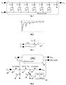
- Fig.1 shows an example of a 6-bit capacitive DAC with an input voltage V in sampled on the top plate before the DAC is switched via the bottom plates of the capacitors to generate the output voltage V out .
- V ref denotes a reference voltage and V offset a fixed offset voltage independent of the input voltage V in
- the coefficients b k correspond to a coarse digitalization of the input voltage V in .
- the non-linearity arises from a mismatch on the coefficients b k which are ideally binary scaled, and from the variation of the reference voltage V ref with the input code b N-1 ...b 0 .
- the coefficients are determined by ratios of capacitors.
- capacitor mismatch introduces linearity errors.
- Various techniques exist to compensate for these errors like calibration, digital compensation or just increasing the area or size of the capacitors to decrease the mismatch.
- a capacitive DAC When a capacitive DAC switches, it draws some charge from the reference node. This amount of charge depends on the code applied at the input of DAC. With an ideal voltage source at the reference, this code-dependent charge does not change the voltage V rej on the reference node. In reality, however, the reference node is either driven by an on-chip buffer or it is connected to an external pin. With an on-chip buffer the voltage on the reference node drops each time the DAC switches and it takes some time to settle to the target reference voltage as shown in Fig.2 . A buffer with a small output impedance is thus needed. The drop depends on the DAC input code b N-1 ...b 0 .
- the settling time is determined by an RC time constant with R the buffer output impedance and C a fraction of the DAC capacitance. To make the DAC linear, one has to wait until the voltage on the reference node is settled close enough to the target reference voltage. This puts a limitation on the speed that can be obtained with the DAC.
- the inductance of the bond wire causes code-dependent ringing on the reference node each time the DAC switches, as shown in Fig.3 .
- extra delay needs to be added before the DAC output can be used with the correct reference voltage.
- a large decoupling capacitor can be put on-chip which requires a significant amount of chip area.
- the fixed capacitor C ref is precharged to the nominal reference voltage V ref and a variable capacitor C aux to a precharge voltage V aux .
- This voltage V aux can be any voltage different from V ref but for practical reasons the most straightforward choice is the electrical ground (zero).
- the required charge for the DAC can be computed as well as the value of C aux required to make the total charge drawn from C ref independent of the selected DAC code.
- the correct mapping of DAC code onto setting for C aux should be implemented as indicated in Fig.4 .
- the proposed scheme also poses some limitations on the ADC in terms of speed and accuracy.
- the DAC needs to go back to the initial situation to be ready for the new sample.
- This DAC resetting also draws a code-dependent charge from the reference capacitor C ref .
- An example for a 6-bit capacitive DAC is shown in Fig.5 . It shows the voltage on the DAC reference node after switching the DAC to generate the residue (squares) including the C aux , and after resetting the DAC back to its initial state (dots).
- C ref is precharged back to V ref with sufficient accuracy over all codes, it needs enough time to settle during the pre-charging phase which results in a speed penalty.
- the optimal value for C aux depends on the DAC characteristics as well as on the reference capacitance C ref and the external voltages V ref and V aux . Due to process variations it is difficult to estimate them with high accuracy and, hence, to know the optimal DAC code mapping onto a setting for C aux . Furthermore, changes in the external reference voltages are not accounted for at all.
- the DAC When the DAC is used in a traditional SAR algorithm, it switches N times and draws N times charge from C ref . Consequently, the compensation with C aux takes N times the time needed to find the correct value for C aux and switch it. Retrieving the correct value for C aux is usually also time-consuming especially when it requires access to a memory. One way to reduce this problem is to use the C aux only in the first few steps of the algorithm.
- Time-interleaving is typically employed to increase the total conversion speed of ADCs.
- the scheme presented in Fig.4 requires a tuneable capacitor C aux for each channel. For large interleaving factors, this results in an increase of the required area.
- the invention relates to a circuit for stabilizing a voltage on a reference node comprising
- the proposed solution allows for optimally setting the variable capacitor.
- Non-ideal effects like parasitics and mismatches, render an optimal mapping very irregular, which makes a highly accurate prediction difficult.
- the proposed scheme requires no exact knowledge of these non-idealities, which makes it generally applicable while still achieving high resolution.
- the actual voltage on the reference node is measured and the result is forwarded to a calibration block where based on the measurement value and the DAC code being received an update is determined for the mapping of the DAC code onto the setting for the variable capacitor value.
- the calibration logic is not so complex, allowing an implementation without significant power consumption increase, which also scales well with technology.
- the measurement block comprises a comparator with programmable offset.
- the programmable offset is advantageously set equal to the difference between a target reference voltage on the reference node and the external reference voltage.
- the circuit is arranged for updating the offset when the variable capacitor reaches a given extreme value.
- the capacitor network further comprises a variable reset capacitor on the reference node arranged for being precharged to a second external auxiliary voltage and for being connected to the reference node when a DAC reset occurs.
- the circuit further comprises an additional quantizer for determining the DAC code.
- the circuit further comprises storage means for storing the updated setting.
- the measurement block comprises an A/D converter.
- the invention in another aspect relates to an analog-to-digital converter comprising a circuit as described above.
- the analog-to-digital converter is implemented as a successive approximation register ADC, a pipelined ADC or a pipelined successive approximation register ADC.
- the analog-to-digital converter comprises a plurality of circuits as previously described and multiplexing means.
- the variable capacitor is common to the plurality of the circuits and connected via the multiplexing means.
- the variable reset capacitor is common to the plurality of the circuits and connected via the multiplexing means.
- to the plurality of said circuits commonly share the measurement block, which is connected via the multiplexing means.
- the present invention is in the first place concerned with proposing a solution for setting the variable capacitor C aux to an optimal value taking into account parasitic effects that are hard to predict during design time, e.g. parasitic capacitances, and also taking into account changes, e.g. due to process variations, in the DAC characteristics and in the external voltages being applied.
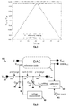
- Fig.6 illustrates an embodiment of the circuit according to the invention.
- a measurement block (40) and a calibration engine (50) are added to the architecture.
- the measurement block is activated after the DAC (10) has been switched for a particular DAC code and C aux programmed with a preliminary setting has been connected to the same node.
- the measurement block measures the resulting voltage on the reference node.
- the measurement block measures the resulting voltage V ref,dac on the reference node and returns a digital word V ref,measured which corresponds to the magnitude of the voltage on the reference node V ref,dac either in absolute terms or relatively to some target reference voltage.
- the measurement block is implemented as an A/D converter. Note that this only differs from an implementation with a comparator by the number of bits used to represent the voltage on the reference node, as the comparator can be seen as a 1-bit ADC.
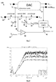
- this measurement block is arranged for performing a comparison of the voltage on the reference node with a target reference voltage level V ref,target ( Fig.7 ).
- the calibration block (50) comprises logic to process the measurement result to update the DAC code mapping onto a setting for the variable capacitor C aux .
- a register in the calibration block is adapted for that DAC code. This register sums the differences of the voltage on the reference node V ref,dac with the target reference voltage U ref,target for that DAC code.
- the register reaches a positive or negative threshold, the total error has become too large and the corresponding setting (32) for C aux for that DAC code is then decreased or increased.
- the value of the threshold is determined by a trade-off between the speed and noise tolerance of the algorithm: a lower threshold updates the setting for C aux more often.
- This calibration runs during normal operation of the DAC. Alternatively, the DAC can be switched offline for each of the available DAC codes and the calibration can be run to find an initial mapping of the DAC code onto setting for C aux .
- Fig.8 shows the DAC accuracy over time expressed by means of three different figures : the effective number of bits (ENOB), spurious-free dynamic range (SFDR) and total harmonic distortion (THD).
- ENOB effective number of bits
- SFDR spurious-free dynamic range
- TDD total harmonic distortion
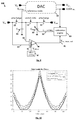
- FIG.9 Another embodiment is shown in Fig.9 .
- the need for an extra input pin to set the target reference level V ref,target as in Fig.7 is avoided.
- a comparator is used in the measurement block, the offset V offset (61) of which can be set by applying a digital word (60).
- the ideal setting for the programmable auxiliary capacitor C aux to achieve the highest resolution in the presence of various parasitic effects depends on the target reference level V ref,target (either set explicitly via an input pin or implicitly by setting the comparator offset V offset ) is illustrated in Fig.10 , showing the best mapping of DAC code b 1 ...b N onto setting for C aux .
- Each curve shows the ideal setting for C aux per DAC code for a different target reference level V ref,target (either explicitly specified as in Fig.7 or implicitly programmed as in Fig.9 ).
- the ideal curve in Fig.10 has an irregular character, the proposed calibration technique is absolutely required in order to achieve high resolution.
- the system can be made completely autonomous by also tuning the comparator offset in the background as shown in Fig.11 . More precisely, the value of the digital word in the comparator is set automatically to implicitly define the target reference voltage V ref,target .
- the scheme in Fig.11 comprises logic (70) to determine whether the selected setting for the programmable auxiliary capacitor C aux is the minimum or maximum setting of the available range and updates the digital word (60) for the offset accordingly.
- the offset (61) is increased or decreased, so that the correct C aux is moved back into the range achievable with the programmable capacitor. For example, when the voltage V aux is ground, the offset should be increased when any C aux setting becomes minimal.
- the measurement block (40) is realized as a comparator with programmable offset (61) with an automatic tuning, an analog mux (93) built with switches to connect the reference nodes of the different channels to one of the comparator inputs, a selector (91) which sends the measurement result to one of the channels, and logic as illustrated in Fig.9 to update the programmable capacitor setting.
- the proposed circuit further comprises a second variable capacitor C aux,rst to stabilize the reference voltage over all DAC codes when resetting the DAC to its initial state.
- a second variable capacitor C aux,rst to stabilize the reference voltage over all DAC codes when resetting the DAC to its initial state.
- an extra programmable capacitor C aux,rst containing a certain number of units is added on the reference node. Its units are first precharged to a voltage V aux,rst (e.g., ground) and when resetting the DAC, the appropriate number of units is connected to the reference node.
- V aux,rst e.g., ground
- the precharge voltage V aux,rst is equal to V aux .
- the required setting depends on the DAC code and is retrieved from the calibration block together with the setting required for C aux without extra time delay. Also, the reset needs to happen anyway, so it does not require extra time.
- the programmable capacitor C aux can be disconnected from the reference node or it can remain connected. This choice only has a small influence on the required values for C aux,rst .
- the capacitive network used to stabilize the reference voltage after resetting the DAC contains the extra programmable capacitor (C aux,rst ), a switch to precharge this programmable capacitor (44), an input pin V aux,rst (which may be the same as input pin V aux or the electrical ground), a switch to connect the programmable capacitor to the DAC reference node during resetting the DAC (45) and a calibration block (50) to map the DAC code b 1 ...b N onto the correct setting for the programmable capacitor C aux,rst .
- Fig.14 illustrates the effect on the voltage variation on the reference node after reset with and without C aux,rst as a function of the resolution of the programmable capacitor C aux,rst .
- the maximum variation of the reference voltage at the DAC input after resetting the DAC to its original state is shown, after it has generated a voltage residue.
- Different points correspond to different resolutions of the programmable capacitor C aux,rst (expressed as the unit size of this capacitor with respect to the unit size of the DAC).
- the dotted curve with stars gives the maximum variation without the programmable capacitor (hence, independent of its resolution).
- the solid curve with squares shows how smaller units (hence, higher resolution) for the programmable capacitor reduce the reference voltage variation. Even with a rather coarse programmable C aux,rst (e.g., a ratio of 1 corresponding to units equal to the units of the main DAC), the variation is greatly reduced.
- Fig.15 illustrates an embodiment that allows using the auxiliary capacitor to stabilize the reference without the requirement to use it during multiple steps of the algorithm.
- the programmable capacitor C aux is only connected once per conversion to the DAC reference node. This happens during the most critical step of the algorithm, namely the final residue generation assuming the residue is to be further quantized.
- the required DAC code b 1 ...b N is then determined with an extra quantizer (8) as shown in Fig.15 .
- This coarse quantizer does not need to be highly linear. Instead, the DAC is linearized by applying the technique of the auxiliary capacitor only when generating the final residue, which can be further processed to achieve higher overall resolution.
- the quantizer (8) can be any type of ADC like a flash, SAR or delta-sigma A/D converter. Since the linearity of the residue is mainly determined by the DAC linearity, this quantizer is non-critical. For example, to achieve 14 bit linearity for a 6-bit DAC, the quantizer needs only to be 6 bit accurate.
- the DAC is often used in an interleaved ADC.
- multiplexers are introduced to reduce the area required for the programmable capacitor.
- Fig.16 illustrates the technique of the programmable auxiliary capacitor C aux in an interleaved system. Instead of applying the technique for each channel individually, it contains a single programmable capacitor C aux , a switch (31) to precharge the programmable capacitor, an input pin V aux to indicate the level to which the programmable capacitor should be precharged (which can be equal to the electrical ground), an analog mux (96) built of switches (11) to connect the programmable capacitor to the reference nodes in the different channels, logic or a memory to map the DAC code in each channel onto a setting for the programmable capacitor, and a multiplexer (92) that subsequently selects the setting for the auxiliary DAC per channel.
- Fig.17 illustrates the use of the programmable auxiliary capacitor C aux,rst during resetting the DAC in an interleaved system.
- it contains a single programmable capacitor C aux,rst , a switch (44) to precharge the programmable auxiliary capacitor, an input pin V aux,rst to indicate the level to which the programmable capacitor should be precharged and which can be equal to pin V aux used for the programmable capacitor used during normal switching of the DAC, or the electrical ground, an analog mux (97) built of switches to connect the programmable capacitor to the reference nodes in the different channels, logic or a memory to map the DAC code in each channel onto a setting for the programmable capacitor, and a multiplexer (98) that subsequently selects the setting for the auxiliary DAC per channel.
- the proposed scheme offers a variety of benefits.
- the area is significantly reduced, as there is no need for a large reference capacitor.
- the overhead of C aux and C aux,rst can be shared among different channels.
- Main part of the power consumption occurs in the logic needed to program the capacitors.
- This purely digital power scales well with technology.
- the calibration technique is not too complex to significantly increase the power consumption.
- the DAC itself does not need to be adapted, which makes the solution generally applicable and independent of DAC parasitics.
- the techniques are also compatible with each other.
- the calibration technique works autonomously without interrupting the normal ADC operation.
- a computer program may be stored/distributed on a suitable medium, such as an optical storage medium or a solid-state medium supplied together with or as part of other hardware, but may also be distributed in other forms, such as via the Internet or other wired or wireless telecommunication systems. Any reference signs in the claims should not be construed as limiting the scope.
Landscapes
- Engineering & Computer Science (AREA)
- Theoretical Computer Science (AREA)
- Physics & Mathematics (AREA)
- Nonlinear Science (AREA)
- Analogue/Digital Conversion (AREA)
Abstract
- a digital-to-analog converter (10), DAC, comprising an array of capacitors and arranged for receiving an input voltage (Vin ) via an input node, a voltage (Vref,DAC ) via a reference node and a DAC code (codeDAC ) via a controller node, said DAC code indicating to which capacitors of the array said voltage (Vref,DAC ) is to be applied, and for outputting a DAC output voltage (Vout ),
- a capacitive network on the reference node comprising a fixed capacitor (Cref ) arranged to be precharged to an external reference voltage (Vref ) and a variable capacitor (Caux ) arranged to be precharged to an external auxiliary voltage (Vaux ) and afterwards to be connected to the reference node,
- a measurement block (40) arranged for measuring the actual voltage on the reference node,
- a calibration block (50) arranged for being fed with the DAC code and the measured actual voltage and for determining an updated setting of the variable capacitor based on the DAC code and the measured actual voltage.
Description
- The present invention is generally related to the field of high speed analog-to digital converters and more particularly to capacitive digital-to-analog converters (DACs) as used therein.
- High-speed analog-to-digital converters (ADCs) often use a capacitive DAC to generate a voltage residue after a coarse conversion that is further quantized to increase the overall conversion resolution. The accuracy for this residue generation is imposed by the required overall accuracy of the total ADC. For example, the DAC used in the first stage of a 14-bit linear ADC pipelined SAR ADC requires more than 14 bit linearity, although its own resolution can be limited to only a few bits.
Fig.1 shows an example of a 6-bit capacitive DAC with an input voltage Vin sampled on the top plate before the DAC is switched via the bottom plates of the capacitors to generate the output voltage Vout. - In general, the output voltage of a DAC as in
Fig.1 above with a resolution of N bits is Vout = Vin - Vdac with
- When a capacitive DAC switches, it draws some charge from the reference node. This amount of charge depends on the code applied at the input of DAC. With an ideal voltage source at the reference, this code-dependent charge does not change the voltage Vrej on the reference node. In reality, however, the reference node is either driven by an on-chip buffer or it is connected to an external pin. With an on-chip buffer the voltage on the reference node drops each time the DAC switches and it takes some time to settle to the target reference voltage as shown in
Fig.2 . A buffer with a small output impedance is thus needed. The drop depends on the DAC input code bN-1...b 0 . The settling time is determined by an RC time constant with R the buffer output impedance and C a fraction of the DAC capacitance. To make the DAC linear, one has to wait until the voltage on the reference node is settled close enough to the target reference voltage. This puts a limitation on the speed that can be obtained with the DAC. - When the reference node is connected to an external pin, the inductance of the bond wire causes code-dependent ringing on the reference node each time the DAC switches, as shown in
Fig.3 . Again, extra delay needs to be added before the DAC output can be used with the correct reference voltage. Alternatively, a large decoupling capacitor can be put on-chip which requires a significant amount of chip area. - It has been proposed in the art to stabilize the reference by adding a capacitive network on the reference node as shown in
Fig.4 . The fixed capacitor Cref is precharged to the nominal reference voltage Vref and a variable capacitor Caux to a precharge voltage Vaux. This voltage Vaux can be any voltage different from Vref but for practical reasons the most straightforward choice is the electrical ground (zero). For a certain DAC configuration and a certain DAC switching event, the required charge for the DAC can be computed as well as the value of Caux required to make the total charge drawn from Cref independent of the selected DAC code. To achieve this code-independent Qref, the correct mapping of DAC code onto setting for Caux should be implemented as indicated inFig.4 . - The proposed scheme, however, also poses some limitations on the ADC in terms of speed and accuracy. After the DAC has switched and the residue has been processed, the DAC needs to go back to the initial situation to be ready for the new sample. This DAC resetting also draws a code-dependent charge from the reference capacitor Cref. An example for a 6-bit capacitive DAC is shown in
Fig.5 . It shows the voltage on the DAC reference node after switching the DAC to generate the residue (squares) including the Caux, and after resetting the DAC back to its initial state (dots). To ensure Cref is precharged back to Vref with sufficient accuracy over all codes, it needs enough time to settle during the pre-charging phase which results in a speed penalty. - The optimal value for Caux depends on the DAC characteristics as well as on the reference capacitance Cref and the external voltages Vref and Vaux. Due to process variations it is difficult to estimate them with high accuracy and, hence, to know the optimal DAC code mapping onto a setting for Caux. Furthermore, changes in the external reference voltages are not accounted for at all.
- When the DAC is used in a traditional SAR algorithm, it switches N times and draws N times charge from Cref . Consequently, the compensation with Caux takes N times the time needed to find the correct value for Caux and switch it. Retrieving the correct value for Caux is usually also time-consuming especially when it requires access to a memory. One way to reduce this problem is to use the Caux only in the first few steps of the algorithm.
- Time-interleaving is typically employed to increase the total conversion speed of ADCs. The scheme presented in
Fig.4 , however, requires a tuneable capacitor Caux for each channel. For large interleaving factors, this results in an increase of the required area. - In a time-interleaved ADC with multiple channels, a different final reference voltage per channel - albeit independent over the codes within a channel - results in gain mismatches between the channels as can be derived from equation (1). These mismatches introduce spurs which limit the overall accuracy. In order to compensate for these gain mismatches, digital correction can be considered but that comes at the cost of a considerably increased complexity.
- Hence, there is room for improvement, so that at least one or more of these drawbacks of the prior art scheme is solved or avoided.
- It is an object of embodiments of the present invention to provide for a stabilizing circuit wherein at least some of the above-mentioned limitations are avoided or overcome.
- The above objective is accomplished by the solution according to the present invention.
- In a first aspect the invention relates to a circuit for stabilizing a voltage on a reference node comprising
- a digital-to-analog converter, DAC, comprising an array of capacitors and arranged for receiving an input voltage via an input node, a voltage via a reference node and a DAC code via a controller node, said DAC code indicating to which capacitors of the array said voltage is to be applied, and for outputting a DAC output voltage,
- a capacitive network on the reference node comprising a fixed capacitor arranged to be precharged to an external reference voltage and a variable capacitor arranged to be precharged to an external auxiliary voltage and to be connected afterwards to the reference node,
- a measurement block arranged for measuring the actual voltage on the reference node,
- a calibration block arranged for being fed with the DAC code and the measured actual voltage and for determining an updated setting of the variable capacitor based on the DAC code and the measured actual voltage.
- The proposed solution allows for optimally setting the variable capacitor. Non-ideal effects, like parasitics and mismatches, render an optimal mapping very irregular, which makes a highly accurate prediction difficult. The proposed scheme requires no exact knowledge of these non-idealities, which makes it generally applicable while still achieving high resolution. The actual voltage on the reference node is measured and the result is forwarded to a calibration block where based on the measurement value and the DAC code being received an update is determined for the mapping of the DAC code onto the setting for the variable capacitor value. The calibration logic is not so complex, allowing an implementation without significant power consumption increase, which also scales well with technology.
- In one embodiment the measurement block comprises a comparator with programmable offset. The programmable offset is advantageously set equal to the difference between a target reference voltage on the reference node and the external reference voltage.
- In an embodiment the circuit is arranged for updating the offset when the variable capacitor reaches a given extreme value.
- In another embodiment the capacitor network further comprises a variable reset capacitor on the reference node arranged for being precharged to a second external auxiliary voltage and for being connected to the reference node when a DAC reset occurs.
- In an embodiment the circuit further comprises an additional quantizer for determining the DAC code.
- In one embodiment the circuit further comprises storage means for storing the updated setting.
- In one embodiment the measurement block comprises an A/D converter.
- In another aspect the invention relates to an analog-to-digital converter comprising a circuit as described above.
- In one embodiment the analog-to-digital converter is implemented as a successive approximation register ADC, a pipelined ADC or a pipelined successive approximation register ADC.
- In another embodiment the analog-to-digital converter comprises a plurality of circuits as previously described and multiplexing means. In one embodiment the variable capacitor is common to the plurality of the circuits and connected via the multiplexing means. Alternatively, the variable reset capacitor is common to the plurality of the circuits and connected via the multiplexing means. In yet another embodiment to the plurality of said circuits commonly share the measurement block, which is connected via the multiplexing means.
- For purposes of summarizing the invention and the advantages achieved over the prior art, certain objects and advantages of the invention have been described herein above. Of course, it is to be understood that not necessarily all such objects or advantages may be achieved in accordance with any particular embodiment of the invention. Thus, for example, those skilled in the art will recognize that the invention may be embodied or carried out in a manner that achieves or optimizes one advantage or group of advantages as taught herein without necessarily achieving other objects or advantages as may be taught or suggested herein.
- The above and other aspects of the invention will be apparent from and elucidated with reference to the embodiment(s) described hereinafter.
- The invention will now be described further, by way of example, with reference to the accompanying drawings, wherein like reference numerals refer to like elements in the various figures.
-
Fig.1 illustrates an example of a capacitive DAC with 6 bit resolution to generate a residue voltage. -
Fig.2 illustrates a reference voltage at the output of an on-chip buffer with a switching capacitive DAC without the use of any reference stabilization technique. -
Fig.3 illustrates a reference voltage connected to an output pin when the DAC switches. -
Fig.4 illustrates a DAC provided with a capacitive network to stabilize the reference voltage as known in the art. -
Fig.5 illustrates a reference voltage at the DAC input after switching the DAC to generate the residue including a capacitive network like the one shown inFig.4 (squares), and the reference voltage after subsequently resetting the DAC to its original state (dots) to be ready for the next sample. -
Fig.6 illustrates an embodiment of the circuit according to the invention. -
Fig.7 illustrates an embodiment of the circuit according to the invention with a comparator or 1-bit ADC used as measurement block. -
Fig.8 illustrates the efficiency of the proposed calibration. -
Fig.9 illustrates an alternative implementation of the invention with a comparator with programmable offset as measurement block. -
Fig.10 represents the ideal settings for the variable auxiliary capacitor Caux. -
Fig.11 illustrates the offset tuning of the comparator used as measurement block. -
Fig.12 illustrates the calibration of the variable capacitor in an interleaved ADC system. -
Fig.13 illustrates the use of a variable capacitor Caux,rst to stabilize the reference voltage after DAC reset. -
Fig.14 illustrates the voltage variation on the reference node with (solid) and without (dotted) CauX,rst . -
Fig.15 illustrates an embodiment with an extra quantizer enabling the use of Caux only for final residue generation. -
Fig.16 illustrates a shared Caux in an interleaved ADC. -
Fig.17 illustrates a shared Caux,rst in an interleaved ADC. - The present invention will be described with respect to particular embodiments and with reference to certain drawings but the invention is not limited thereto but only by the claims.
- Furthermore, the terms first, second and the like in the description and in the claims, are used for distinguishing between similar elements and not necessarily for describing a sequence, either temporally, spatially, in ranking or in any other manner. It is to be understood that the terms so used are interchangeable under appropriate circumstances and that the embodiments of the invention described herein are capable of operation in other sequences than described or illustrated herein.
- It is to be noticed that the term "comprising", used in the claims, should not be interpreted as being restricted to the means listed thereafter; it does not exclude other elements or steps. It is thus to be interpreted as specifying the presence of the stated features, integers, steps or components as referred to, but does not preclude the presence or addition of one or more other features, integers, steps or components, or groups thereof. Thus, the scope of the expression "a device comprising means A and B" should not be limited to devices consisting only of components A and B. It means that with respect to the present invention, the only relevant components of the device are A and B.
- Reference throughout this specification to "one embodiment" or "an embodiment" means that a particular feature, structure or characteristic described in connection with the embodiment is included in at least one embodiment of the present invention. Thus, appearances of the phrases "in one embodiment" or "in an embodiment" in various places throughout this specification are not necessarily all referring to the same embodiment, but may. Furthermore, the particular features, structures or characteristics may be combined in any suitable manner, as would be apparent to one of ordinary skill in the art from this disclosure, in one or more embodiments.
- Similarly it should be appreciated that in the description of exemplary embodiments of the invention, various features of the invention are sometimes grouped together in a single embodiment, figure, or description thereof for the purpose of streamlining the disclosure and aiding in the understanding of one or more of the various inventive aspects. This method of disclosure, however, is not to be interpreted as reflecting an intention that the claimed invention requires more features than are expressly recited in each claim. Rather, as the following claims reflect, inventive aspects lie in less than all features of a single foregoing disclosed embodiment. Thus, the claims following the detailed description are hereby expressly incorporated into this detailed description, with each claim standing on its own as a separate embodiment of this invention.
- Furthermore, while some embodiments described herein include some but not other features included in other embodiments, combinations of features of different embodiments are meant to be within the scope of the invention, and form different embodiments, as would be understood by those in the art. For example, in the following claims, any of the claimed embodiments can be used in any combination.
- It should be noted that the use of particular terminology when describing certain features or aspects of the invention should not be taken to imply that the terminology is being redefined herein to be restricted to include any specific characteristics of the features or aspects of the invention with which that terminology is associated.
- In the description provided herein, numerous specific details are set forth. However, it is understood that embodiments of the invention may be practiced without these specific details. In other instances, well-known methods, structures and techniques have not been shown in detail in order not to obscure an understanding of this description.
- The present invention is in the first place concerned with proposing a solution for setting the variable capacitor Caux to an optimal value taking into account parasitic effects that are hard to predict during design time, e.g. parasitic capacitances, and also taking into account changes, e.g. due to process variations, in the DAC characteristics and in the external voltages being applied.
- Accurate prediction of the charge drawn by the DAC and, hence, a correct setting for the programmable capacitor Caux is a difficult task. Mismatches, parasitics or variations of the external reference voltages change the ideal value. Furthermore, the variable (in certain embodiments, programmable) capacitor itself suffers from mismatches as well. Making these mismatches small would require large capacitor values resulting in large area, which clearly is no viable option. Furthermore, with the precharge voltage Vaux equal to zero, large values for Caux would result in a large drop from the nominal Vref to the stabilized reference voltage.
- The invention proposes a scheme that allows achieving high accuracy in the presence of various parasitic effects like parasitic capacitances, mismatches and voltage variations.
Fig.6 illustrates an embodiment of the circuit according to the invention. Compared to the prior art scheme ofFig.4 a measurement block (40) and a calibration engine (50) are added to the architecture. The measurement block is activated after the DAC (10) has been switched for a particular DAC code and Caux programmed with a preliminary setting has been connected to the same node. The measurement block measures the resulting voltage on the reference node. The measurement block measures the resulting voltage Vref,dac on the reference node and returns a digital word Vref,measured which corresponds to the magnitude of the voltage on the reference node Vref,dac either in absolute terms or relatively to some target reference voltage. In one embodiment the measurement block is implemented as an A/D converter. Note that this only differs from an implementation with a comparator by the number of bits used to represent the voltage on the reference node, as the comparator can be seen as a 1-bit ADC. In another embodiment this measurement block is arranged for performing a comparison of the voltage on the reference node with a target reference voltage level Vref,target (Fig.7 ). The calibration block (50) comprises logic to process the measurement result to update the DAC code mapping onto a setting for the variable capacitor Caux. Depending on the measurement result, a register in the calibration block is adapted for that DAC code. This register sums the differences of the voltage on the reference node Vref,dac with the target reference voltage Uref,target for that DAC code. When the register reaches a positive or negative threshold, the total error has become too large and the corresponding setting (32) for Caux for that DAC code is then decreased or increased. The value of the threshold is determined by a trade-off between the speed and noise tolerance of the algorithm: a lower threshold updates the setting for Caux more often. This calibration runs during normal operation of the DAC. Alternatively, the DAC can be switched offline for each of the available DAC codes and the calibration can be run to find an initial mapping of the DAC code onto setting for Caux. - The efficiency of the proposed calibration is illustrated in
Fig.8 , where the accuracy increases until saturation, limited by the resolution of Caux.Fig.8 shows the DAC accuracy over time expressed by means of three different figures : the effective number of bits (ENOB), spurious-free dynamic range (SFDR) and total harmonic distortion (THD). Over time, the settings for the programmable auxiliary capacitor are updated and the accuracy increases until it settles to a maximum value determined by the resolution of the programmable auxiliary capacitor. - Another embodiment is shown in
Fig.9 . In this embodiment with a comparator as measurement block (40) the need for an extra input pin to set the target reference level Vref,target as inFig.7 is avoided. A comparator is used in the measurement block, the offset Voffset (61) of which can be set by applying a digital word (60). When the comparator compares with the external reference voltage Vref already available in the system, it effectively compares to a target reference level of Uref,target = Vref - Voffset. So, the offset corresponds to the difference between the nominal reference voltage Vref and the resulting voltage on the reference node of the DAC after switching. This is not a large value, so a traditional comparator with offset tuning can be employed. - The ideal setting for the programmable auxiliary capacitor Caux to achieve the highest resolution in the presence of various parasitic effects depends on the target reference level Vref,target (either set explicitly via an input pin or implicitly by setting the comparator offset Voffset ) is illustrated in
Fig.10 , showing the best mapping of DAC code b1...bN onto setting for Caux. Each curve shows the ideal setting for Caux per DAC code for a different target reference level Vref,target (either explicitly specified as inFig.7 or implicitly programmed as inFig.9 ). As the ideal curve inFig.10 has an irregular character, the proposed calibration technique is absolutely required in order to achieve high resolution. - When setting the target reference level via the offset programming of the comparator, the system can be made completely autonomous by also tuning the comparator offset in the background as shown in
Fig.11 . More precisely, the value of the digital word in the comparator is set automatically to implicitly define the target reference voltage Vref,target. The scheme inFig.11 comprises logic (70) to determine whether the selected setting for the programmable auxiliary capacitor Caux is the minimum or maximum setting of the available range and updates the digital word (60) for the offset accordingly. When any setting for Caux reaches a minimum or maximum value, the offset (61) is increased or decreased, so that the correct Caux is moved back into the range achievable with the programmable capacitor. For example, when the voltage Vaux is ground, the offset should be increased when any Caux setting becomes minimal. - From equation (1) it is clear that the residue voltage is proportional to the voltage on the DAC reference node. In the case of an interleaved ADC, stabilization of the reference voltage to different reference values consequently results in gain mismatches between the channels of the interleaved ADC. Such mismatches result in spurs in the output spectrum limiting the ADC resolution. To solve this, an analog multiplexer (93) is introduced to subsequently select the reference node of the DACs in the interleaved channels as shown in
Fig.12 . Also, a demux (91) is added to send the measurement result to the calibration engine of the right channel. By using a common measurement block (40) to measure the voltage on the reference node and updating the settings for Caux accordingly, this technique ensures there is no gain mismatch anymore between the different channels. InFig.12 an embodiment is shown with the measurement block (40) is realized as a comparator with programmable offset (61) with an automatic tuning, an analog mux (93) built with switches to connect the reference nodes of the different channels to one of the comparator inputs, a selector (91) which sends the measurement result to one of the channels, and logic as illustrated inFig.9 to update the programmable capacitor setting. - In one embodiment the proposed circuit further comprises a second variable capacitor C aux,rst to stabilize the reference voltage over all DAC codes when resetting the DAC to its initial state. This ensures that even when there is insufficient time during precharging for complete settling of the voltage on Cref to Vref, the settling error is always the same and, hence, independent of the DAC code. Consequently, no non-linear errors are introduced.
Fig.13 illustrates this embodiment. - More in particular, an extra programmable capacitor Caux,rst containing a certain number of units is added on the reference node. Its units are first precharged to a voltage Vaux,rst (e.g., ground) and when resetting the DAC, the appropriate number of units is connected to the reference node. In one embodiment the precharge voltage Vaux,rst is equal to Vaux. The required setting depends on the DAC code and is retrieved from the calibration block together with the setting required for Caux without extra time delay. Also, the reset needs to happen anyway, so it does not require extra time. During the reset operation, the programmable capacitor Caux can be disconnected from the reference node or it can remain connected. This choice only has a small influence on the required values for Caux,rst.
- The capacitive network used to stabilize the reference voltage after resetting the DAC contains the extra programmable capacitor (Caux,rst), a switch to precharge this programmable capacitor (44), an input pin Vaux,rst (which may be the same as input pin Vaux or the electrical ground), a switch to connect the programmable capacitor to the DAC reference node during resetting the DAC (45) and a calibration block (50) to map the DAC code b1...bN onto the correct setting for the programmable capacitor Caux,rst.
-
Fig.14 illustrates the effect on the voltage variation on the reference node after reset with and without Caux,rst as a function of the resolution of the programmable capacitor C aux,rst . The maximum variation of the reference voltage at the DAC input after resetting the DAC to its original state is shown, after it has generated a voltage residue. Different points correspond to different resolutions of the programmable capacitor Caux,rst (expressed as the unit size of this capacitor with respect to the unit size of the DAC). The dotted curve with stars gives the maximum variation without the programmable capacitor (hence, independent of its resolution). The solid curve with squares shows how smaller units (hence, higher resolution) for the programmable capacitor reduce the reference voltage variation. Even with a rather coarse programmable Caux,rst (e.g., a ratio of 1 corresponding to units equal to the units of the main DAC), the variation is greatly reduced. -
Fig.15 illustrates an embodiment that allows using the auxiliary capacitor to stabilize the reference without the requirement to use it during multiple steps of the algorithm. In order to reduce the time delay as much as possible, the programmable capacitor Caux is only connected once per conversion to the DAC reference node. This happens during the most critical step of the algorithm, namely the final residue generation assuming the residue is to be further quantized. The required DAC code b1...bN is then determined with an extra quantizer (8) as shown inFig.15 . This coarse quantizer does not need to be highly linear. Instead, the DAC is linearized by applying the technique of the auxiliary capacitor only when generating the final residue, which can be further processed to achieve higher overall resolution. The quantizer (8) can be any type of ADC like a flash, SAR or delta-sigma A/D converter. Since the linearity of the residue is mainly determined by the DAC linearity, this quantizer is non-critical. For example, to achieve 14 bit linearity for a 6-bit DAC, the quantizer needs only to be 6 bit accurate. - For high-speed operation the DAC is often used in an interleaved ADC. For this configuration, multiplexers are introduced to reduce the area required for the programmable capacitor.
-
Fig.16 illustrates the technique of the programmable auxiliary capacitor Caux in an interleaved system. Instead of applying the technique for each channel individually, it contains a single programmable capacitor Caux, a switch (31) to precharge the programmable capacitor, an input pin Vaux to indicate the level to which the programmable capacitor should be precharged (which can be equal to the electrical ground), an analog mux (96) built of switches (11) to connect the programmable capacitor to the reference nodes in the different channels, logic or a memory to map the DAC code in each channel onto a setting for the programmable capacitor, and a multiplexer (92) that subsequently selects the setting for the auxiliary DAC per channel. -
Fig.17 illustrates the use of the programmable auxiliary capacitor C aux,rst during resetting the DAC in an interleaved system. Instead of applying the technique for each channel individually, it contains a single programmable capacitor C aux,rst, a switch (44) to precharge the programmable auxiliary capacitor, an input pin Vaux,rst to indicate the level to which the programmable capacitor should be precharged and which can be equal to pin Vaux used for the programmable capacitor used during normal switching of the DAC, or the electrical ground, an analog mux (97) built of switches to connect the programmable capacitor to the reference nodes in the different channels, logic or a memory to map the DAC code in each channel onto a setting for the programmable capacitor, and a multiplexer (98) that subsequently selects the setting for the auxiliary DAC per channel. - The proposed scheme offers a variety of benefits. The area is significantly reduced, as there is no need for a large reference capacitor. In a time-interleaved ADC the overhead of Caux and Caux,rst can be shared among different channels. There is no significant increase in power consumption. Main part of the power consumption occurs in the logic needed to program the capacitors. This purely digital power scales well with technology. Also, the calibration technique is not too complex to significantly increase the power consumption. The DAC itself does not need to be adapted, which makes the solution generally applicable and independent of DAC parasitics. The techniques are also compatible with each other. The calibration technique works autonomously without interrupting the normal ADC operation.
- While the invention has been illustrated and described in detail in the drawings and foregoing description, such illustration and description are to be considered illustrative or exemplary and not restrictive. The foregoing description details certain embodiments of the invention. It will be appreciated, however, that no matter how detailed the foregoing appears in text, the invention may be practiced in many ways. The invention is not limited to the disclosed embodiments.
- Other variations to the disclosed embodiments can be understood and effected by those skilled in the art in practicing the claimed invention, from a study of the drawings, the disclosure and the appended claims. In the claims, the word "comprising" does not exclude other elements or steps, and the indefinite article "a" or "an" does not exclude a plurality. A single processor or other unit may fulfil the functions of several items recited in the claims. The mere fact that certain measures are recited in mutually different dependent claims does not indicate that a combination of these measures cannot be used to advantage. A computer program may be stored/distributed on a suitable medium, such as an optical storage medium or a solid-state medium supplied together with or as part of other hardware, but may also be distributed in other forms, such as via the Internet or other wired or wireless telecommunication systems. Any reference signs in the claims should not be construed as limiting the scope.
Claims (15)
- Circuit (100) for stabilizing a voltage on a reference node comprising- a digital-to-analog converter (10), DAC, comprising an array of capacitors and arranged for receiving an input voltage (Vin ) via an input node, a voltage (Vref,DAC ) via a reference node and a DAC code (codeDAc) via a controller node, said DAC code indicating to which capacitors of said array said voltage (Vref,DAC ) is to be applied, and for outputting a DAC output voltage (Vout ),- a capacitive network on said reference node comprising a fixed capacitor (Cref ) arranged to be precharged to an external reference voltage (Vref ) and a variable capacitor (Caux ) arranged to be precharged to an external auxiliary voltage (Vaux ) and afterwards to be connected to said reference node,- a measurement block (40) arranged for measuring the actual voltage on said reference node,- a calibration block (50) arranged for being fed with said DAC code and said measured actual voltage and for determining an updated setting of said variable capacitor based on said DAC code and said measured actual voltage.
- Circuit as in claim 1, wherein said measurement block comprises a comparator arranged to compare said voltage (Vref,DAC ) on said reference node with an external target reference voltage (Vrep,target ).
- Circuit as in claim 1 or 2, wherein said measurement block comprises a comparator with programmable offset.
- Circuit as in claim 3, wherein said programmable offset is set equal to the difference between a target reference voltage (Vref,target) on said reference node and said external reference voltage.
- Circuit as in any of the previous claims, arranged for updating said offset when said variable capacitor (Caux ) reaches a given extreme value.
- Circuit as in any of the previous claims, wherein said capacitor network further comprises a variable reset capacitor (Caux,rst ) on said reference node arranged for being precharged to a second external auxiliary voltage (Vaux,rst ) and for being connected to said reference node when the DAC resets.
- Circuit as in any of the previous claims, further comprising an additional quantizer (8) for determining said DAC code.
- Circuit as in any of the previous claims, wherein said measurement block comprises an analog-to-digital converter.
- Circuit as in any of the previous claims, further comprising storage means for storing said updated setting.
- Analog-to-digital converter, ADC, comprising said circuit as in any of the previous claims.
- Analog-to-digital converter as in claim 10, implemented as a successive approximation register ADC, a pipelined ADC or a pipelined successive approximation register ADC.
- Analog-to-digital converter as in claim 10 or 11, comprising a plurality of said circuits as in any of claims 1 to 8, and multiplexing means.
- Analog-to-digital converter as in claim 12, wherein said variable capacitor (Caux ) is common to said plurality of said circuits and connected via said multiplexing means.
- Analog-to-digital converter as in claim 12, wherein said variable reset capacitor (Caux,rst ) is common to said plurality of said circuits and connected via said multiplexing means.
- Analog-to-digital converter as in claim 12, wherein said measurement block (40) is common to said plurality of said circuits and connected via said multiplexing means.
Priority Applications (2)
| Application Number | Priority Date | Filing Date | Title |
|---|---|---|---|
| EP15200700.1A EP3182593B1 (en) | 2015-12-17 | 2015-12-17 | Circuit for stabilizing a dac reference voltage |
| US15/373,578 US9800258B2 (en) | 2015-12-17 | 2016-12-09 | Circuit for stabilizing a digital-to-analog converter reference voltage |
Applications Claiming Priority (1)
| Application Number | Priority Date | Filing Date | Title |
|---|---|---|---|
| EP15200700.1A EP3182593B1 (en) | 2015-12-17 | 2015-12-17 | Circuit for stabilizing a dac reference voltage |
Publications (2)
| Publication Number | Publication Date |
|---|---|
| EP3182593A1 true EP3182593A1 (en) | 2017-06-21 |
| EP3182593B1 EP3182593B1 (en) | 2019-02-27 |
Family
ID=54850243
Family Applications (1)
| Application Number | Title | Priority Date | Filing Date |
|---|---|---|---|
| EP15200700.1A Active EP3182593B1 (en) | 2015-12-17 | 2015-12-17 | Circuit for stabilizing a dac reference voltage |
Country Status (2)
| Country | Link |
|---|---|
| US (1) | US9800258B2 (en) |
| EP (1) | EP3182593B1 (en) |
Cited By (2)
| Publication number | Priority date | Publication date | Assignee | Title |
|---|---|---|---|---|
| CN114070320A (en) * | 2020-08-03 | 2022-02-18 | 知微电子有限公司 | Non-linear digital-to-analog converter |
| EP4170910A1 (en) * | 2018-01-19 | 2023-04-26 | Socionext Inc. | Processing circuitry |
Families Citing this family (8)
| Publication number | Priority date | Publication date | Assignee | Title |
|---|---|---|---|---|
| US10156596B2 (en) * | 2015-12-10 | 2018-12-18 | Microchip Technology Incorporated | Voltage measurement circuit |
| US10218268B1 (en) | 2018-03-26 | 2019-02-26 | Analog Devices Global Unlimited Company | Voltage reference circuit and method of providing a voltage reference |
| JP7142341B2 (en) * | 2018-04-16 | 2022-09-27 | ザインエレクトロニクス株式会社 | AD converter |
| US10541698B1 (en) * | 2018-11-08 | 2020-01-21 | Analog Devices, Inc. | Switched capacitor multiplying digital-to-analog converter |
| CN110535473B (en) * | 2019-09-03 | 2022-04-22 | 中国电子科技集团公司第二十四研究所 | Non-acquisition-guarantee high-speed high-input-bandwidth pipeline structure ADC without path mismatch |
| CN114079465B (en) * | 2020-08-12 | 2024-08-20 | 财团法人成大研究发展基金会 | Step-by-step analog-to-digital converter |
| US11831328B2 (en) * | 2022-02-07 | 2023-11-28 | Pixart Imaging Inc. | Electronic device and method capable of predicting and generating compensation charge amount(s) in response to switching of CDAC |
| JP2023118555A (en) * | 2022-02-15 | 2023-08-25 | 株式会社ソシオネクスト | Analog-to-digital conversion circuits and semiconductor integrated circuits |
Citations (1)
| Publication number | Priority date | Publication date | Assignee | Title |
|---|---|---|---|---|
| US9154151B1 (en) * | 2014-12-22 | 2015-10-06 | Altera Corporation | Analog-to-digital converter circuits and methods |
Family Cites Families (1)
| Publication number | Priority date | Publication date | Assignee | Title |
|---|---|---|---|---|
| US9223332B1 (en) * | 2013-09-10 | 2015-12-29 | Maxim Integrated Products, Inc. | Stabilizing reference voltage of switched capacitor circuits |
-
2015
- 2015-12-17 EP EP15200700.1A patent/EP3182593B1/en active Active
-
2016
- 2016-12-09 US US15/373,578 patent/US9800258B2/en active Active
Patent Citations (1)
| Publication number | Priority date | Publication date | Assignee | Title |
|---|---|---|---|---|
| US9154151B1 (en) * | 2014-12-22 | 2015-10-06 | Altera Corporation | Analog-to-digital converter circuits and methods |
Non-Patent Citations (2)
| Title |
|---|
| DUSAN VLASTIMIR STEPANOVIC: "Calibration Techniques for Time-Interleaved SAR A/D Converters", 4 December 2012 (2012-12-04), XP055245116, ISBN: 978-1-267-97564-5, Retrieved from the Internet <URL:http://digitalassets.lib.berkeley.edu/techreports/ucb/text/EECS-2012-225.pdf> [retrieved on 20160127] * |
| INIYAVAN ELUMALAI: "A Capacitance-Based Reference Scheme for a 14b-Linear, 100 MS/s SAR-Assisted Pipeline ADC", 21 August 2012 (2012-08-21), XP055281565, Retrieved from the Internet <URL:http://repository.tudelft.nl/islandora/object/uuid:8b94e22b-cd51-407c-af86-9c2389f20e4c/datastream/OBJ/download> [retrieved on 20160617] * |
Cited By (2)
| Publication number | Priority date | Publication date | Assignee | Title |
|---|---|---|---|---|
| EP4170910A1 (en) * | 2018-01-19 | 2023-04-26 | Socionext Inc. | Processing circuitry |
| CN114070320A (en) * | 2020-08-03 | 2022-02-18 | 知微电子有限公司 | Non-linear digital-to-analog converter |
Also Published As
| Publication number | Publication date |
|---|---|
| US20170179974A1 (en) | 2017-06-22 |
| EP3182593B1 (en) | 2019-02-27 |
| US9800258B2 (en) | 2017-10-24 |
Similar Documents
| Publication | Publication Date | Title |
|---|---|---|
| US9800258B2 (en) | Circuit for stabilizing a digital-to-analog converter reference voltage | |
| KR102174204B1 (en) | Successive approximation register and single-slope analog-digital converting apparatus and method, and cmos image sensor thereof | |
| US9432044B1 (en) | Mismatch correction of attenuation capacitor in a successive approximation register analog to digital converter | |
| KR102637630B1 (en) | Redundancy scheme for flash assisted successive approximation register(sar) analog-to-digital converter(adc) | |
| US5675340A (en) | Charge-redistribution analog-to-digital converter with reduced comparator-hysteresis effects | |
| US10840934B2 (en) | Methods and apparatus for a successive approximation register analog-to-digital converter | |
| US6486807B2 (en) | A/D converter calibration | |
| EP3537609B1 (en) | Method of applying a dither, and analog to digital converter operating in accordance with the method | |
| US10886937B1 (en) | Method to embed ELD DAC in SAR quantizer | |
| US10069506B2 (en) | Calibration circuit and calibration method for DAC | |
| EP2629429A1 (en) | A/D converter and method for calibrating the same | |
| US20130044014A1 (en) | Successive approximation analog to digital converter with capacitor mismatch calibration and method thereof | |
| TWI482438B (en) | Successive approximation analog to digital converter and method thereof | |
| EP3059867A1 (en) | Circuit and method for dac mismatch error detection and correction in an adc | |
| US20100001892A1 (en) | Successive approximation a/d converter | |
| US9300312B2 (en) | Analog-digital converter | |
| EP3613147B1 (en) | Successive approximation register (sar) analog to digital converter (adc) | |
| KR20160058140A (en) | Pipelined successive approximation analog to digital converter | |
| KR20160080355A (en) | Analog-digital converter for error correction | |
| US20110187573A1 (en) | Time-multiplexed residue amplifier | |
| CN111313903A (en) | Successive Approximation Register (SAR) analog-to-digital converter (ADC) dynamic range extension | |
| KR101711542B1 (en) | Range-scaled composite pipeline analog-to-digital converter | |
| US20250030432A1 (en) | Analog-to-digital converters and methods for settling of the reference voltage in analog-to-digital converters | |
| US11637558B2 (en) | Analog-to-digital converter capable of reducing nonlinearity and method of operating the same | |
| US11476858B2 (en) | Advanced successive approximation register analog-to-digital converter and corresponding method |
Legal Events
| Date | Code | Title | Description |
|---|---|---|---|
| PUAI | Public reference made under article 153(3) epc to a published international application that has entered the european phase |
Free format text: ORIGINAL CODE: 0009012 |
|
| STAA | Information on the status of an ep patent application or granted ep patent |
Free format text: STATUS: THE APPLICATION HAS BEEN PUBLISHED |
|
| AK | Designated contracting states |
Kind code of ref document: A1 Designated state(s): AL AT BE BG CH CY CZ DE DK EE ES FI FR GB GR HR HU IE IS IT LI LT LU LV MC MK MT NL NO PL PT RO RS SE SI SK SM TR |
|
| AX | Request for extension of the european patent |
Extension state: BA ME |
|
| STAA | Information on the status of an ep patent application or granted ep patent |
Free format text: STATUS: REQUEST FOR EXAMINATION WAS MADE |
|
| 17P | Request for examination filed |
Effective date: 20171207 |
|
| RBV | Designated contracting states (corrected) |
Designated state(s): AL AT BE BG CH CY CZ DE DK EE ES FI FR GB GR HR HU IE IS IT LI LT LU LV MC MK MT NL NO PL PT RO RS SE SI SK SM TR |
|
| GRAP | Despatch of communication of intention to grant a patent |
Free format text: ORIGINAL CODE: EPIDOSNIGR1 |
|
| STAA | Information on the status of an ep patent application or granted ep patent |
Free format text: STATUS: GRANT OF PATENT IS INTENDED |
|
| RIC1 | Information provided on ipc code assigned before grant |
Ipc: H03M 1/46 20060101ALN20180516BHEP Ipc: H03M 1/10 20060101AFI20180516BHEP |
|
| RIC1 | Information provided on ipc code assigned before grant |
Ipc: H03M 1/46 20060101ALN20180518BHEP Ipc: H03M 1/10 20060101AFI20180518BHEP |
|
| INTG | Intention to grant announced |
Effective date: 20180612 |
|
| GRAJ | Information related to disapproval of communication of intention to grant by the applicant or resumption of examination proceedings by the epo deleted |
Free format text: ORIGINAL CODE: EPIDOSDIGR1 |
|
| STAA | Information on the status of an ep patent application or granted ep patent |
Free format text: STATUS: REQUEST FOR EXAMINATION WAS MADE |
|
| INTC | Intention to grant announced (deleted) | ||
| GRAP | Despatch of communication of intention to grant a patent |
Free format text: ORIGINAL CODE: EPIDOSNIGR1 |
|
| STAA | Information on the status of an ep patent application or granted ep patent |
Free format text: STATUS: GRANT OF PATENT IS INTENDED |
|
| INTG | Intention to grant announced |
Effective date: 20180914 |
|
| RIC1 | Information provided on ipc code assigned before grant |
Ipc: H03M 1/46 20060101ALN20180831BHEP Ipc: H03M 1/10 20060101AFI20180831BHEP |
|
| GRAS | Grant fee paid |
Free format text: ORIGINAL CODE: EPIDOSNIGR3 |
|
| GRAA | (expected) grant |
Free format text: ORIGINAL CODE: 0009210 |
|
| STAA | Information on the status of an ep patent application or granted ep patent |
Free format text: STATUS: THE PATENT HAS BEEN GRANTED |
|
| AK | Designated contracting states |
Kind code of ref document: B1 Designated state(s): AL AT BE BG CH CY CZ DE DK EE ES FI FR GB GR HR HU IE IS IT LI LT LU LV MC MK MT NL NO PL PT RO RS SE SI SK SM TR |
|
| REG | Reference to a national code |
Ref country code: GB Ref legal event code: FG4D |
|
| REG | Reference to a national code |
Ref country code: CH Ref legal event code: EP |
|
| REG | Reference to a national code |
Ref country code: AT Ref legal event code: REF Ref document number: 1102817 Country of ref document: AT Kind code of ref document: T Effective date: 20190315 |
|
| REG | Reference to a national code |
Ref country code: IE Ref legal event code: FG4D |
|
| REG | Reference to a national code |
Ref country code: DE Ref legal event code: R096 Ref document number: 602015025289 Country of ref document: DE |
|
| REG | Reference to a national code |
Ref country code: NL Ref legal event code: MP Effective date: 20190227 |
|
| REG | Reference to a national code |
Ref country code: LT Ref legal event code: MG4D |
|
| PG25 | Lapsed in a contracting state [announced via postgrant information from national office to epo] |
Ref country code: SE Free format text: LAPSE BECAUSE OF FAILURE TO SUBMIT A TRANSLATION OF THE DESCRIPTION OR TO PAY THE FEE WITHIN THE PRESCRIBED TIME-LIMIT Effective date: 20190227 Ref country code: PT Free format text: LAPSE BECAUSE OF FAILURE TO SUBMIT A TRANSLATION OF THE DESCRIPTION OR TO PAY THE FEE WITHIN THE PRESCRIBED TIME-LIMIT Effective date: 20190627 Ref country code: NO Free format text: LAPSE BECAUSE OF FAILURE TO SUBMIT A TRANSLATION OF THE DESCRIPTION OR TO PAY THE FEE WITHIN THE PRESCRIBED TIME-LIMIT Effective date: 20190527 Ref country code: FI Free format text: LAPSE BECAUSE OF FAILURE TO SUBMIT A TRANSLATION OF THE DESCRIPTION OR TO PAY THE FEE WITHIN THE PRESCRIBED TIME-LIMIT Effective date: 20190227 Ref country code: LT Free format text: LAPSE BECAUSE OF FAILURE TO SUBMIT A TRANSLATION OF THE DESCRIPTION OR TO PAY THE FEE WITHIN THE PRESCRIBED TIME-LIMIT Effective date: 20190227 |
|
| PG25 | Lapsed in a contracting state [announced via postgrant information from national office to epo] |
Ref country code: GR Free format text: LAPSE BECAUSE OF FAILURE TO SUBMIT A TRANSLATION OF THE DESCRIPTION OR TO PAY THE FEE WITHIN THE PRESCRIBED TIME-LIMIT Effective date: 20190528 Ref country code: BG Free format text: LAPSE BECAUSE OF FAILURE TO SUBMIT A TRANSLATION OF THE DESCRIPTION OR TO PAY THE FEE WITHIN THE PRESCRIBED TIME-LIMIT Effective date: 20190527 Ref country code: RS Free format text: LAPSE BECAUSE OF FAILURE TO SUBMIT A TRANSLATION OF THE DESCRIPTION OR TO PAY THE FEE WITHIN THE PRESCRIBED TIME-LIMIT Effective date: 20190227 Ref country code: NL Free format text: LAPSE BECAUSE OF FAILURE TO SUBMIT A TRANSLATION OF THE DESCRIPTION OR TO PAY THE FEE WITHIN THE PRESCRIBED TIME-LIMIT Effective date: 20190227 Ref country code: IS Free format text: LAPSE BECAUSE OF FAILURE TO SUBMIT A TRANSLATION OF THE DESCRIPTION OR TO PAY THE FEE WITHIN THE PRESCRIBED TIME-LIMIT Effective date: 20190627 Ref country code: HR Free format text: LAPSE BECAUSE OF FAILURE TO SUBMIT A TRANSLATION OF THE DESCRIPTION OR TO PAY THE FEE WITHIN THE PRESCRIBED TIME-LIMIT Effective date: 20190227 Ref country code: LV Free format text: LAPSE BECAUSE OF FAILURE TO SUBMIT A TRANSLATION OF THE DESCRIPTION OR TO PAY THE FEE WITHIN THE PRESCRIBED TIME-LIMIT Effective date: 20190227 |
|
| REG | Reference to a national code |
Ref country code: AT Ref legal event code: MK05 Ref document number: 1102817 Country of ref document: AT Kind code of ref document: T Effective date: 20190227 |
|
| PG25 | Lapsed in a contracting state [announced via postgrant information from national office to epo] |
Ref country code: SK Free format text: LAPSE BECAUSE OF FAILURE TO SUBMIT A TRANSLATION OF THE DESCRIPTION OR TO PAY THE FEE WITHIN THE PRESCRIBED TIME-LIMIT Effective date: 20190227 Ref country code: RO Free format text: LAPSE BECAUSE OF FAILURE TO SUBMIT A TRANSLATION OF THE DESCRIPTION OR TO PAY THE FEE WITHIN THE PRESCRIBED TIME-LIMIT Effective date: 20190227 Ref country code: EE Free format text: LAPSE BECAUSE OF FAILURE TO SUBMIT A TRANSLATION OF THE DESCRIPTION OR TO PAY THE FEE WITHIN THE PRESCRIBED TIME-LIMIT Effective date: 20190227 Ref country code: IT Free format text: LAPSE BECAUSE OF FAILURE TO SUBMIT A TRANSLATION OF THE DESCRIPTION OR TO PAY THE FEE WITHIN THE PRESCRIBED TIME-LIMIT Effective date: 20190227 Ref country code: DK Free format text: LAPSE BECAUSE OF FAILURE TO SUBMIT A TRANSLATION OF THE DESCRIPTION OR TO PAY THE FEE WITHIN THE PRESCRIBED TIME-LIMIT Effective date: 20190227 Ref country code: ES Free format text: LAPSE BECAUSE OF FAILURE TO SUBMIT A TRANSLATION OF THE DESCRIPTION OR TO PAY THE FEE WITHIN THE PRESCRIBED TIME-LIMIT Effective date: 20190227 Ref country code: AL Free format text: LAPSE BECAUSE OF FAILURE TO SUBMIT A TRANSLATION OF THE DESCRIPTION OR TO PAY THE FEE WITHIN THE PRESCRIBED TIME-LIMIT Effective date: 20190227 Ref country code: CZ Free format text: LAPSE BECAUSE OF FAILURE TO SUBMIT A TRANSLATION OF THE DESCRIPTION OR TO PAY THE FEE WITHIN THE PRESCRIBED TIME-LIMIT Effective date: 20190227 |
|
| REG | Reference to a national code |
Ref country code: DE Ref legal event code: R097 Ref document number: 602015025289 Country of ref document: DE |
|
| PG25 | Lapsed in a contracting state [announced via postgrant information from national office to epo] |
Ref country code: PL Free format text: LAPSE BECAUSE OF FAILURE TO SUBMIT A TRANSLATION OF THE DESCRIPTION OR TO PAY THE FEE WITHIN THE PRESCRIBED TIME-LIMIT Effective date: 20190227 Ref country code: SM Free format text: LAPSE BECAUSE OF FAILURE TO SUBMIT A TRANSLATION OF THE DESCRIPTION OR TO PAY THE FEE WITHIN THE PRESCRIBED TIME-LIMIT Effective date: 20190227 |
|
| PG25 | Lapsed in a contracting state [announced via postgrant information from national office to epo] |
Ref country code: AT Free format text: LAPSE BECAUSE OF FAILURE TO SUBMIT A TRANSLATION OF THE DESCRIPTION OR TO PAY THE FEE WITHIN THE PRESCRIBED TIME-LIMIT Effective date: 20190227 |
|
| PLBE | No opposition filed within time limit |
Free format text: ORIGINAL CODE: 0009261 |
|
| STAA | Information on the status of an ep patent application or granted ep patent |
Free format text: STATUS: NO OPPOSITION FILED WITHIN TIME LIMIT |
|
| 26N | No opposition filed |
Effective date: 20191128 |
|
| PG25 | Lapsed in a contracting state [announced via postgrant information from national office to epo] |
Ref country code: SI Free format text: LAPSE BECAUSE OF FAILURE TO SUBMIT A TRANSLATION OF THE DESCRIPTION OR TO PAY THE FEE WITHIN THE PRESCRIBED TIME-LIMIT Effective date: 20190227 |
|
| PG25 | Lapsed in a contracting state [announced via postgrant information from national office to epo] |
Ref country code: TR Free format text: LAPSE BECAUSE OF FAILURE TO SUBMIT A TRANSLATION OF THE DESCRIPTION OR TO PAY THE FEE WITHIN THE PRESCRIBED TIME-LIMIT Effective date: 20190227 |
|
| REG | Reference to a national code |
Ref country code: CH Ref legal event code: PL |
|
| REG | Reference to a national code |
Ref country code: BE Ref legal event code: MM Effective date: 20191231 |
|
| PG25 | Lapsed in a contracting state [announced via postgrant information from national office to epo] |
Ref country code: MC Free format text: LAPSE BECAUSE OF FAILURE TO SUBMIT A TRANSLATION OF THE DESCRIPTION OR TO PAY THE FEE WITHIN THE PRESCRIBED TIME-LIMIT Effective date: 20190227 |
|
| PG25 | Lapsed in a contracting state [announced via postgrant information from national office to epo] |
Ref country code: IE Free format text: LAPSE BECAUSE OF NON-PAYMENT OF DUE FEES Effective date: 20191217 Ref country code: LU Free format text: LAPSE BECAUSE OF NON-PAYMENT OF DUE FEES Effective date: 20191217 |
|
| PG25 | Lapsed in a contracting state [announced via postgrant information from national office to epo] |
Ref country code: CH Free format text: LAPSE BECAUSE OF NON-PAYMENT OF DUE FEES Effective date: 20191231 Ref country code: BE Free format text: LAPSE BECAUSE OF NON-PAYMENT OF DUE FEES Effective date: 20191231 Ref country code: LI Free format text: LAPSE BECAUSE OF NON-PAYMENT OF DUE FEES Effective date: 20191231 |
|
| PG25 | Lapsed in a contracting state [announced via postgrant information from national office to epo] |
Ref country code: CY Free format text: LAPSE BECAUSE OF FAILURE TO SUBMIT A TRANSLATION OF THE DESCRIPTION OR TO PAY THE FEE WITHIN THE PRESCRIBED TIME-LIMIT Effective date: 20190227 |
|
| PG25 | Lapsed in a contracting state [announced via postgrant information from national office to epo] |
Ref country code: HU Free format text: LAPSE BECAUSE OF FAILURE TO SUBMIT A TRANSLATION OF THE DESCRIPTION OR TO PAY THE FEE WITHIN THE PRESCRIBED TIME-LIMIT; INVALID AB INITIO Effective date: 20151217 Ref country code: MT Free format text: LAPSE BECAUSE OF FAILURE TO SUBMIT A TRANSLATION OF THE DESCRIPTION OR TO PAY THE FEE WITHIN THE PRESCRIBED TIME-LIMIT Effective date: 20190227 |
|
| PG25 | Lapsed in a contracting state [announced via postgrant information from national office to epo] |
Ref country code: MK Free format text: LAPSE BECAUSE OF FAILURE TO SUBMIT A TRANSLATION OF THE DESCRIPTION OR TO PAY THE FEE WITHIN THE PRESCRIBED TIME-LIMIT Effective date: 20190227 |
|
| P01 | Opt-out of the competence of the unified patent court (upc) registered |
Effective date: 20230513 |
|
| PGFP | Annual fee paid to national office [announced via postgrant information from national office to epo] |
Ref country code: DE Payment date: 20251126 Year of fee payment: 11 |
|
| PGFP | Annual fee paid to national office [announced via postgrant information from national office to epo] |
Ref country code: GB Payment date: 20251119 Year of fee payment: 11 |
|
| PGFP | Annual fee paid to national office [announced via postgrant information from national office to epo] |
Ref country code: FR Payment date: 20251119 Year of fee payment: 11 |