EP3182583A2 - Oscillator scheme capable of reducing far-out phase noise and closed-in phase noise - Google Patents
Oscillator scheme capable of reducing far-out phase noise and closed-in phase noise Download PDFInfo
- Publication number
- EP3182583A2 EP3182583A2 EP16198335.8A EP16198335A EP3182583A2 EP 3182583 A2 EP3182583 A2 EP 3182583A2 EP 16198335 A EP16198335 A EP 16198335A EP 3182583 A2 EP3182583 A2 EP 3182583A2
- Authority
- EP
- European Patent Office
- Prior art keywords
- port
- capacitor
- oscillator
- resonator
- transconductance amplifier
- Prior art date
- Legal status (The legal status is an assumption and is not a legal conclusion. Google has not performed a legal analysis and makes no representation as to the accuracy of the status listed.)
- Granted
Links
Images



Classifications
-
- H—ELECTRICITY
- H03—ELECTRONIC CIRCUITRY
- H03B—GENERATION OF OSCILLATIONS, DIRECTLY OR BY FREQUENCY-CHANGING, BY CIRCUITS EMPLOYING ACTIVE ELEMENTS WHICH OPERATE IN A NON-SWITCHING MANNER; GENERATION OF NOISE BY SUCH CIRCUITS
- H03B1/00—Details
- H03B1/04—Reducing undesired oscillations, e.g. harmonics
-
- H—ELECTRICITY
- H03—ELECTRONIC CIRCUITRY
- H03B—GENERATION OF OSCILLATIONS, DIRECTLY OR BY FREQUENCY-CHANGING, BY CIRCUITS EMPLOYING ACTIVE ELEMENTS WHICH OPERATE IN A NON-SWITCHING MANNER; GENERATION OF NOISE BY SUCH CIRCUITS
- H03B5/00—Generation of oscillations using amplifier with regenerative feedback from output to input
- H03B5/02—Details
- H03B5/04—Modifications of generator to compensate for variations in physical values, e.g. power supply, load, temperature
-
- H—ELECTRICITY
- H03—ELECTRONIC CIRCUITRY
- H03B—GENERATION OF OSCILLATIONS, DIRECTLY OR BY FREQUENCY-CHANGING, BY CIRCUITS EMPLOYING ACTIVE ELEMENTS WHICH OPERATE IN A NON-SWITCHING MANNER; GENERATION OF NOISE BY SUCH CIRCUITS
- H03B5/00—Generation of oscillations using amplifier with regenerative feedback from output to input
-
- H—ELECTRICITY
- H03—ELECTRONIC CIRCUITRY
- H03B—GENERATION OF OSCILLATIONS, DIRECTLY OR BY FREQUENCY-CHANGING, BY CIRCUITS EMPLOYING ACTIVE ELEMENTS WHICH OPERATE IN A NON-SWITCHING MANNER; GENERATION OF NOISE BY SUCH CIRCUITS
- H03B5/00—Generation of oscillations using amplifier with regenerative feedback from output to input
- H03B5/08—Generation of oscillations using amplifier with regenerative feedback from output to input with frequency-determining element comprising lumped inductance and capacitance
- H03B5/12—Generation of oscillations using amplifier with regenerative feedback from output to input with frequency-determining element comprising lumped inductance and capacitance active element in amplifier being semiconductor device
-
- H—ELECTRICITY
- H03—ELECTRONIC CIRCUITRY
- H03B—GENERATION OF OSCILLATIONS, DIRECTLY OR BY FREQUENCY-CHANGING, BY CIRCUITS EMPLOYING ACTIVE ELEMENTS WHICH OPERATE IN A NON-SWITCHING MANNER; GENERATION OF NOISE BY SUCH CIRCUITS
- H03B5/00—Generation of oscillations using amplifier with regenerative feedback from output to input
- H03B5/30—Generation of oscillations using amplifier with regenerative feedback from output to input with frequency-determining element being electromechanical resonator
- H03B5/32—Generation of oscillations using amplifier with regenerative feedback from output to input with frequency-determining element being electromechanical resonator being a piezoelectric resonator
- H03B5/36—Generation of oscillations using amplifier with regenerative feedback from output to input with frequency-determining element being electromechanical resonator being a piezoelectric resonator active element in amplifier being semiconductor device
- H03B5/362—Generation of oscillations using amplifier with regenerative feedback from output to input with frequency-determining element being electromechanical resonator being a piezoelectric resonator active element in amplifier being semiconductor device the amplifier being a single transistor
-
- H—ELECTRICITY
- H03—ELECTRONIC CIRCUITRY
- H03B—GENERATION OF OSCILLATIONS, DIRECTLY OR BY FREQUENCY-CHANGING, BY CIRCUITS EMPLOYING ACTIVE ELEMENTS WHICH OPERATE IN A NON-SWITCHING MANNER; GENERATION OF NOISE BY SUCH CIRCUITS
- H03B5/00—Generation of oscillations using amplifier with regenerative feedback from output to input
- H03B5/30—Generation of oscillations using amplifier with regenerative feedback from output to input with frequency-determining element being electromechanical resonator
- H03B5/32—Generation of oscillations using amplifier with regenerative feedback from output to input with frequency-determining element being electromechanical resonator being a piezoelectric resonator
- H03B5/36—Generation of oscillations using amplifier with regenerative feedback from output to input with frequency-determining element being electromechanical resonator being a piezoelectric resonator active element in amplifier being semiconductor device
- H03B5/366—Generation of oscillations using amplifier with regenerative feedback from output to input with frequency-determining element being electromechanical resonator being a piezoelectric resonator active element in amplifier being semiconductor device and comprising means for varying the frequency by a variable voltage or current
-
- H—ELECTRICITY
- H03—ELECTRONIC CIRCUITRY
- H03L—AUTOMATIC CONTROL, STARTING, SYNCHRONISATION OR STABILISATION OF GENERATORS OF ELECTRONIC OSCILLATIONS OR PULSES
- H03L5/00—Automatic control of voltage, current, or power
-
- H—ELECTRICITY
- H03—ELECTRONIC CIRCUITRY
- H03B—GENERATION OF OSCILLATIONS, DIRECTLY OR BY FREQUENCY-CHANGING, BY CIRCUITS EMPLOYING ACTIVE ELEMENTS WHICH OPERATE IN A NON-SWITCHING MANNER; GENERATION OF NOISE BY SUCH CIRCUITS
- H03B2200/00—Indexing scheme relating to details of oscillators covered by H03B
- H03B2200/006—Functional aspects of oscillators
- H03B2200/0062—Bias and operating point
-
- H—ELECTRICITY
- H03—ELECTRONIC CIRCUITRY
- H03B—GENERATION OF OSCILLATIONS, DIRECTLY OR BY FREQUENCY-CHANGING, BY CIRCUITS EMPLOYING ACTIVE ELEMENTS WHICH OPERATE IN A NON-SWITCHING MANNER; GENERATION OF NOISE BY SUCH CIRCUITS
- H03B2200/00—Indexing scheme relating to details of oscillators covered by H03B
- H03B2200/006—Functional aspects of oscillators
- H03B2200/0088—Reduction of noise
- H03B2200/009—Reduction of phase noise
Definitions
- the present invention relates to an oscillator scheme, and more particularly to an oscillator apparatus capable of reducing far-out phase noise as well as closed-in phase noise according to the pre-characterizing clauses of claim 1.
- a conventional two-pin oscillator such as a conventional Pierces oscillator is arranged to generate and output a smaller voltage signal to a next stage circuit.
- the smaller amplitude may avoid active devices such as transistors to be affected by nonlinearity effects.
- the smaller amplitude also means that the device driving capability of the conventional Pierces oscillator is limited.
- the conventional Pierces oscillator is unable to reduce far-out phase noise (e.g. frequency offsets above 10KHz).
- the far-out phase noise e.g.
- the present invention aims at providing an oscillator apparatus capable of reducing far-out phase noise and closed-in phase noise, to solve the above-mentioned problems.
- the claimed oscillator apparatus includes an oscillator core circuit.
- the oscillator core circuit includes an inverting transconductance amplifier, at least one first capacitor, at least one second capacitor, and a resonator.
- the at least one first capacitor is connected between an input of the inverting transconductance amplifier and a ground level.
- the at least one second capacitor is connected between an output of the inverting transconductance amplifier and the ground level.
- the resonator has the first port connected to the input of the inverting transconductance amplifier and the second port connected to the output of the inverting transconductance amplifier. The first port is decoupled from the second port. So the common mode of two ports can be defined independently.
- the capacitance of the at least one first capacitor is further configured to be smaller than that of the at least one second capacitor.
- the amplitude of a voltage signal at the first port of the resonator is further larger than that of a voltage signal at the second port of the resonator.
- the oscillator apparatus further comprises a DC coupling circuit and a driver.
- the DC coupling circuit is placed between the oscillator core circuit and the driver, so there is no AC coupling capacitors and its loss.
- FIG. 1 is a diagram of an oscillator apparatus 100 according to a first embodiment of the invention.
- the oscillator apparatus 100 is a two-pin oscillator apparatus (not limited) and/or an on-chip oscillator apparatus (not limited).
- the oscillator apparatus 100 is capable of reducing far-out phase noise as well as reducing closed-in phase noise.
- the definition of far-out phase noise refers to the phase/offset noise far from a specified frequency such as frequency offset(s) higher than 10KHz
- the definition of closed-in phase noise for example refers to the frequency offset component that is within the neighborhood of the specified frequency, e.g. frequency offset (s) lower than 100Hz.
- the oscillator apparatus 100 is able to achieve both far-out and closed-in phase noise improvements.
- the phase noise improvements are achieved by enhancing devices' driving capability, providing sufficient signal amplitude for a driver, and avoiding active devices entering non-linear operating region (triode region); these are described later.
- the oscillator apparatus 100 comprises an oscillator core circuit 105, a driver 110, a bias circuit 115, and a DC coupling circuit 120 placed between oscillator core circuit 105 and driver 110.
- the driver 110 can be implemented by a squarer, an inverter buffer, or a voltage gain buffer, and so on.
- the oscillator core circuit 105 comprises a current source 1051, an inverting transconductance amplifier 1052 with a negative transconductance gain -Gm, at least one first capacitor 1053A, at least one second capacitor 1053B, and a resonator 1054.
- the inverting transconductance amplifier 1052 with negative transconductance gain -Gm can be implemented by any kinds of active devices such as MOS transistors and/or bipolar transistors.
- the oscillator core circuit 105 includes one first capacitor 1053A with capacitance C1 and one second capacitor 1053B with capacitance C2.
- the oscillator core circuit 105 can be configured to include a first capacitor array 1053A having multiple first capacitors with different capacitances and a second capacitor array 1053B having multiple second capacitors with different capacitances.
- the number of first capacitor (s) 1053A and/or number of second capacitor (s) 1053B is not meant to be a limitation of the invention.
- the first capacitor 1053A is connected between the input of the inverting transconductance amplifier 1052 and a ground level GND
- the second capacitor 1053B is connected between the output of the inverting transconductance amplifier 1052 and the ground level GND.
- the resonator 1054 includes a first end/node/port connected to the input of the inverting transconductance amplifier 1052 and a second end/node/port connected to the output of the inverting transconductance amplifier 1052.
- the first port of resonator 1054 is decoupled from its second port wherein the first port corresponds to the voltage signal VX1 and the second port corresponds to the voltage signal VX2; as shown in FIG.
- no feedback circuits are placed between the first port and second port of resonator 1054.
- the DC voltage bias level at the first port is not dependent upon and not controlled based on the DC voltage bias level at the second port.
- the voltage signal VX1 generated at the first port of oscillator core circuit 105 is transmitted to the driver 110 via the DC coupling circuit 120 and is biased by the bias circuit 115.
- the voltage signals VX1 and VX2 generate a signal VO on the resonator 1054.
- the first port of resonator 1054 can be DC coupled to the driver 110, and no AC coupling circuits are needed.
- the DC coupling circuit 120 can be implemented by using a wire and/or a resistor to pass the full spectrum of signal including direct current to the driver 110.
- No AC coupling capacitors are used as high-pass filters
- the bias circuit 115 can be implemented by using a low noise bias circuit to provide a bias voltage with low noise as the common mode voltage for the oscillator core circuit 105 and driver 110.
- the bias circuit 115 is connected to the first port of resonator 1054 and configured to provide the common mode voltage to the first port of resonator 1054. Even though the noise of bias circuit 115 is transmitted to the oscillator core circuit 105, the far-out phase noise can still be suppressed by resonator 1054.
- the input of the driver 110 is DC coupled to the input of the inverting transconductance amplifier 1052 and the first port of the resonator 1054.
- the driver 110 generates and outputs a square-wave signal at its output node based on the waveform of the voltage signals VX1 generated from the first port of resonator 1054.
- the oscillator apparatus 100 provides the square-wave signal for a next stage circuit as a reference clock signal.
- the DC coupling circuit 120 is employed and connected between the driver 110 and the first port of resonator 1054 since the first port is decoupled from the second port (i.e. no feedback paths between voltage signals VX1 and VX2). Capacitor (s) used for AC coupling can be eliminated, and the voltage signal VX1 transmitted to the driver 110 is not attenuated by the AC coupling capacitor (s) .
- the capacitance C1 of first capacitor 1053A is configured to be smaller than the capacitance C2 of second capacitor 1053B.
- the capacitors 1053A and 1053B can be implemented on a chip.
- the capacitances C1 and C2 can be digitally controlled.
- AX1 and AX2 respectively indicate the amplitudes (i.e. the swings) of voltage signals VX1 and VX2 at two ports of resonator 1054.
- the amplitude AX1 of voltage signal VX1 is inversely proportional to the capacitance C1
- the amplitude AX2 of voltage signal VX2 is inversely proportional to the capacitance C2.
- the ratio of amplitude AX1 to amplitude AX2 is enlarged since of the larger capacitance C2 and smaller capacitance C1. This configuration can effectively avoid the current source 1051 entering the triode region as well as avoiding the inverting transconductance amplifier 1052 entering the triode region, which induces non-linear effects.
- FIG. 2 is an equivalent circuit diagram of the oscillator core circuit 105 as shown in FIG. 1 .
- FIG. 3 is a diagram illustrating the operating regions of the current source 1051 and inverting transconductance amplifier 1052 of FIG. 1 .
- the resonator 1054 comprises the resistor Rp, inductor Lp, and capacitor Cp.
- the amplitude AX1 of voltage signal VX1 is enlarged and larger than the amplitude AX2 of voltage signal VX2 because the capacitance C2 is configured to be larger than capacitance C1.
- FIG. 1 is an equivalent circuit diagram of the oscillator core circuit 105 as shown in FIG. 1 .
- FIG. 3 is a diagram illustrating the operating regions of the current source 1051 and inverting transconductance amplifier 1052 of FIG. 1 .
- the resonator 1054 comprises the resistor Rp, inductor Lp, and capacitor Cp.
- the amplitude AX1 of voltage signal VX1 is enlarged and larger than the
- the two swings represented by dotted curves indicate the voltage swings at two ports of a conventional oscillator
- two swings represented by solid curves indicate the voltage amplitudes (AX1 and AX2) at two ports of the resonator 1054.
- a block 205A surrounded by dotted lines includes operating regions of triode region and saturation region, and this represents that there is a great possibility that active devices of the conventional oscillator may enter the triode region frequently and performances of the active devices are degraded due to closed-in phase noise.
- the amplitude AX1 is enlarged, and the amplitude AX2 is reduced.
- active devices of current source 1051 and inverting transconductance amplifier 1052 can be maintained or kept in the saturation region which is represented a block 205B surrounded by solid lines and including slanting lines as shown in FIG. 3 . That is, the operating regions of the active devices can be kept within the saturation region almost for whole operating cycles of the active devices. This significantly reduces the possibility that the active devices enter the triode region and degrades closed-in phase noise as far as possible.
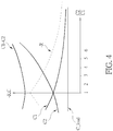
- FIG. 4 is a diagram illustrating a relation between different negative resistance conditions of resonator 1054 and different choices of the ratio of C2 to C1 according to the embodiment of FIG. 1 .
- the dotted curve of FIG. 4 indicates the value of negative resistance -R, and the value of negative resistance -R is at the maximum value when the capacitance C1 is equal to C2.
- the maximum value of negative resistance -R indicates an optimal start-up condition for a conventional oscillator, and the conventional oscillator is arranged to operate under the optimal start-up condition (i.e. adopting the maximum value of negative resistance -R) as far as possible.
- the optimal start-up condition i.e. adopting the maximum value of negative resistance -R
- the capacitance C2 of second capacitor 1053B is configured to be larger than the capacitance C1 of first capacitor 1053A, and the ratio of C2 to C1 is configured to be higher than one, for example 1.1 or 1.2.
- the sum of C1 and C2 can be designed/configured to become larger when the ratio of C2 to C1 becomes higher, as shown in FIG. 4 .
- the ratio of C2 to C1 is designed or configured to be higher than 1.1 considering that actual capacitance variations in percentage may vary from -10% to +10%.
- the ratio of C2 to C1 is configured to be higher than value of 1.2. That is, the lower bound of ratio C2 to C1 is configured as 1.1 or 1.2.
- the upper bound of ratio C2 to C1 can be determined based on the design requirements of the negative resistance/capacitance (-R) and the total capacitor area.
- the first capacitor 1053A can be implemented with a voltage independent linear capacitor, which is unchanged with the variation of a voltage swing actually.
- the second capacitor 1053B can be implemented with a high density capacitor, which has the capacitance is moderately changed by voltage swing. For example, if the capacitance of a high density capacitor is as four times as that of a linear capacitor.
- the required total capacitor area is as 2.4 times as the required area of a linear capacitor when the ratio of C2 to C1 is equal to one and the first capacitor 1053A and the second capacitor 1053B both are implemented by linear capacitors.
- the required total capacitor area is as 2.5 times as the required circuit area of the linear capacitor when the ratio of C2 to C1 is equal to 1. 5 and the first capacitor 1053A and second capacitor 1053B both are implemented by linear capacitors .
- the capacitor area may be a little larger than original one as expected.
- the required total capacitor area can be decreased as 1.375 times as the required circuit area of the linear capacitor if the first capacitor 1053A and the second capacitor 1053B are implemented by a linear capacitor and a high density capacitor respectively. That is, this invention can save chip area of capacitor as well as achieving degradation of the signal-to-noise ratio (SNR).
- SNR signal-to-noise ratio
- the linear capacitor can be implemented by a metal insulator metal (MIM) capacitor or a metal oxide metal (MOM) capacitor (but not limited).
- MIM metal insulator metal
- MOM metal oxide metal
- the high density capacitor can be implemented by a metal oxide semiconductor (MOS) capacitor (but not limited) . All these can take advantage that the oscillator apparatus 100 can be operated at a low voltage level and/or the active devices of oscillator apparatus 100 can be manufactured by using a low cost process.
- FIG. 5 is a diagram of an oscillator apparatus 400 according to a second embodiment of the invention.
- the oscillator apparatus 400 can be a two-pin oscillator apparatus (not limited) and/or an on-chip oscillator apparatus (not limited).
- the oscillator apparatus 400 is capable of reducing far-out phase noise as well as reducing closed-in phase noise.
- the oscillator apparatus 400 comprises an oscillator core circuit 405, the driver 110, the bias circuit 115, and the Dc coupling circuit 120 placed between oscillator core circuit 105 and driver 110.
- the oscillator core circuit 405 comprises the current source 1051, the inverting transconductance amplifier 1052 with negative transconductance gain -Gm, the first switched capacitor array 4053A, the second switched capacitor array 4053B, and the resonator 1054.
- the first switched capacitor array 4053A comprises a plurality of switches S11-S1n and a plurality of first capacitors with different/equal capacitances C11-Cln.
- the second switched capacitor array 4053B comprises a plurality of switches S21-S2m and a plurality of second capacitors with different/equal capacitances C21-C2m. Parameters n and m are positive integers and can be equal to each other or be different.
- the oscillator apparatus 400 can be used for providing an output signal with different oscillation frequencies.
- the inverting transconductance amplifier 1052 can be implemented by using an NMOS transistor having a control node connected to the first port of resonator 1054, a first node connected to the current source 1052 and second port of resonator 1054, and a second node connected to the ground level.
- FIG. 6 is a diagram illustrating another implementation of the oscillator apparatus 400 as shown in FIG. 5 .
- the inverting transconductance amplifier 1052 within apparatus 400 is implemented by using complementary MOS structure circuit.
- the inverting transconductance amplifier 1052 of FIG. 6 comprises a NMOS transistor and a PMOS transistor.
- the PMOS transistor includes a control node connected to the first port of resonator 1054, a first node connected to the current source 1051, and a second node connected to the second port of resonator 1054.
- the NMOS transistor includes a control node connected to the first port of resonator 1054, a first node connected to the second port of resonator 1054 and second node of the PMOS transistor, and a second node connected to the ground level.
- the bias circuit 115 can be implemented by various kinds of circuits.
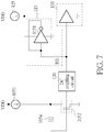
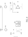
- FIG. 7 and FIG. 8 respectively illustrate different embodiments of the bias circuit 115 as shown in FIG. 1 .
- the bias circuit 115 comprises a resistor RB and an inverter 1151.
- the inverter size is selected according to consideration of low-noise and optimal bias point.
- the resistor RB is coupled between the Dc coupling circuit 120 and the inverter 1151, and the resistor RB used as a high impedance/resistance to avoid noise loaded to the resonator 1054.
- the inverter 1151 includes an input node coupled to the resistor RB and connected to its output node.
- the inverter 1151 can be biased and controlled by a specific current provided from a current source 125 that is also used for providing the specific voltage to bias and control the driver 110.
- the bias circuit 115 comprises the resistor RB that is connected between the input node of driver 110 and the output node of driver 110.
- the upper bound limit of the ratio of C2 to C1 can be determined/calculated based on a frequency tuning range, load capacitance C_load, and the negative resistance -R specified above.
- the lower bound limit of the ratio of C2 to C1 is determined/calculated to avoid the active devices entering the triode region.
Landscapes
- Inductance-Capacitance Distribution Constants And Capacitance-Resistance Oscillators (AREA)
Abstract
Description
- The present invention relates to an oscillator scheme, and more particularly to an oscillator apparatus capable of reducing far-out phase noise as well as closed-in phase noise according to the pre-characterizing clauses of
claim 1. - In order to reduce closed-in phase noise (e.g. frequency offsets below 100Hz), a conventional two-pin oscillator such as a conventional Pierces oscillator is arranged to generate and output a smaller voltage signal to a next stage circuit. The smaller amplitude may avoid active devices such as transistors to be affected by nonlinearity effects. However, the smaller amplitude (voltage swing) also means that the device driving capability of the conventional Pierces oscillator is limited. The conventional Pierces oscillator is unable to reduce far-out phase noise (e.g. frequency offsets above 10KHz). On the other hand, in order to reduce the far-out phase noise (e.g. frequency offsets above 10KHz), another type of conventional Pierces oscillator is arranged to generate and output a larger voltage signal to a next stage circuit. The larger amplitude improves the device driving capability, but the larger amplitude (voltage swing) unfortunately causes active devices to be affected by the nonlinearity effects. This type of conventional Pierces oscillator is incapable of reducing closed-in phase noise. Thus, both the Pierces oscillators now developed by current industry are unable to reduce far-out phase noise as well as closed-in phase noise simultaneously.
- This in mind, the present invention aims at providing an oscillator apparatus capable of reducing far-out phase noise and closed-in phase noise, to solve the above-mentioned problems.
- This is achieved by an oscillator apparatus according to
claim 1. The respective dependent claims pertain to corresponding further development and improvements. - As will be seen more clearly from the detailed description following below, the claimed oscillator apparatus includes an oscillator core circuit. The oscillator core circuit includes an inverting transconductance amplifier, at least one first capacitor, at least one second capacitor, and a resonator. The at least one first capacitor is connected between an input of the inverting transconductance amplifier and a ground level. The at least one second capacitor is connected between an output of the inverting transconductance amplifier and the ground level. The resonator has the first port connected to the input of the inverting transconductance amplifier and the second port connected to the output of the inverting transconductance amplifier. The first port is decoupled from the second port. So the common mode of two ports can be defined independently.
- Additionally, the capacitance of the at least one first capacitor is further configured to be smaller than that of the at least one second capacitor.
- Additionally, the amplitude of a voltage signal at the first port of the resonator is further larger than that of a voltage signal at the second port of the resonator.
- Additionally, the oscillator apparatus further comprises a DC coupling circuit and a driver. The DC coupling circuit is placed between the oscillator core circuit and the driver, so there is no AC coupling capacitors and its loss.
- In the following, the invention is further illustrated by way of example, taking reference to the accompanying drawings. Thereof
-
FIG. 1 is a diagram of an oscillator apparatus according to a first embodiment of the invention. -
FIG. 2 is an equivalent circuit diagram of the oscillator core circuit as shown inFIG. 1 . -
FIG. 3 is a diagram illustrating the operating regions of the current source and inverting transconductance amplifier ofFIG. 1 . -
FIG. 4 is a diagram illustrating a relation between different negative resistance of resonator and different ratio of C2 over C1 according to the embodiment ofFIG. 1 . -
FIG. 5 is a diagram of an oscillator apparatus according to the second embodiment of the invention. -
FIG. 6 is a diagram illustrating another implementation of the oscillator apparatus as shown inFIG. 5 . -
FIG. 7 is a diagram illustrating an embodiment of the bias circuit as shown inFIG. 1 . -
FIG. 8 is a diagram illustrating another embodiment of the bias circuit as shown inFIG. 1 . - Please refer to
FIG. 1 , which is a diagram of anoscillator apparatus 100 according to a first embodiment of the invention. In the embodiment, theoscillator apparatus 100 is a two-pin oscillator apparatus (not limited) and/or an on-chip oscillator apparatus (not limited). Theoscillator apparatus 100 is capable of reducing far-out phase noise as well as reducing closed-in phase noise. The definition of far-out phase noise, for example, refers to the phase/offset noise far from a specified frequency such as frequency offset(s) higher than 10KHz, and the definition of closed-in phase noise for example refers to the frequency offset component that is within the neighborhood of the specified frequency, e.g. frequency offset (s) lower than 100Hz. It should be noted that the above-mentioned examples of offset frequencies are used for illustrative purposes and are not intended to be limitations of the invention. Theoscillator apparatus 100 is able to achieve both far-out and closed-in phase noise improvements. In this embodiment, the phase noise improvements are achieved by enhancing devices' driving capability, providing sufficient signal amplitude for a driver, and avoiding active devices entering non-linear operating region (triode region); these are described later. - In practice, the
oscillator apparatus 100 comprises anoscillator core circuit 105, adriver 110, abias circuit 115, and aDC coupling circuit 120 placed betweenoscillator core circuit 105 anddriver 110. Thedriver 110 can be implemented by a squarer, an inverter buffer, or a voltage gain buffer, and so on. Theoscillator core circuit 105 comprises acurrent source 1051, an invertingtransconductance amplifier 1052 with a negative transconductance gain -Gm, at least onefirst capacitor 1053A, at least onesecond capacitor 1053B, and aresonator 1054. The invertingtransconductance amplifier 1052 with negative transconductance gain -Gm can be implemented by any kinds of active devices such as MOS transistors and/or bipolar transistors. In this embodiment, theoscillator core circuit 105 includes onefirst capacitor 1053A with capacitance C1 and onesecond capacitor 1053B with capacitance C2. In other embodiments, theoscillator core circuit 105 can be configured to include afirst capacitor array 1053A having multiple first capacitors with different capacitances and asecond capacitor array 1053B having multiple second capacitors with different capacitances. The number of first capacitor (s) 1053A and/or number of second capacitor (s) 1053B is not meant to be a limitation of the invention. In this embodiment, thefirst capacitor 1053A is connected between the input of the invertingtransconductance amplifier 1052 and a ground level GND, and thesecond capacitor 1053B is connected between the output of the invertingtransconductance amplifier 1052 and the ground level GND. Theresonator 1054 includes a first end/node/port connected to the input of the invertingtransconductance amplifier 1052 and a second end/node/port connected to the output of the invertingtransconductance amplifier 1052. The first port ofresonator 1054 is decoupled from its second port wherein the first port corresponds to the voltage signal VX1 and the second port corresponds to the voltage signal VX2; as shown inFIG. 1 , no feedback circuits are placed between the first port and second port ofresonator 1054. The DC voltage bias level at the first port is not dependent upon and not controlled based on the DC voltage bias level at the second port. The voltage signal VX1 generated at the first port ofoscillator core circuit 105 is transmitted to thedriver 110 via theDC coupling circuit 120 and is biased by thebias circuit 115. The voltage signals VX1 and VX2 generate a signal VO on theresonator 1054. In practice, the signal VO of theresonator 1054 can be determined based on the following equations:


wherein C1 is the capacitance offirst capacitor 1053A, and C2 is the capacitance ofsecond capacitor 1053B. - Via the
DC coupling circuit 120, the first port ofresonator 1054 can be DC coupled to thedriver 110, and no AC coupling circuits are needed. In practice, theDC coupling circuit 120 can be implemented by using a wire and/or a resistor to pass the full spectrum of signal including direct current to thedriver 110. No AC coupling capacitors are used as high-pass filters, and thebias circuit 115 can be implemented by using a low noise bias circuit to provide a bias voltage with low noise as the common mode voltage for theoscillator core circuit 105 anddriver 110. As shown inFIG. 1 , thebias circuit 115 is connected to the first port ofresonator 1054 and configured to provide the common mode voltage to the first port ofresonator 1054. Even though the noise ofbias circuit 115 is transmitted to theoscillator core circuit 105, the far-out phase noise can still be suppressed byresonator 1054. - The input of the
driver 110 is DC coupled to the input of the invertingtransconductance amplifier 1052 and the first port of theresonator 1054. Thedriver 110 generates and outputs a square-wave signal at its output node based on the waveform of the voltage signals VX1 generated from the first port ofresonator 1054. Theoscillator apparatus 100 provides the square-wave signal for a next stage circuit as a reference clock signal. - For far-out phase noise improvement, instead of using AC coupling blocks, the
DC coupling circuit 120 is employed and connected between thedriver 110 and the first port ofresonator 1054 since the first port is decoupled from the second port (i.e. no feedback paths between voltage signals VX1 and VX2). Capacitor (s) used for AC coupling can be eliminated, and the voltage signal VX1 transmitted to thedriver 110 is not attenuated by the AC coupling capacitor (s) . - For far-out and closed-in phase noise improvements, in this embodiment, the capacitance C1 of
first capacitor 1053A is configured to be smaller than the capacitance C2 ofsecond capacitor 1053B. Thecapacitors 
- AX1 and AX2 respectively indicate the amplitudes (i.e. the swings) of voltage signals VX1 and VX2 at two ports of
resonator 1054. The amplitude AX1 of voltage signal VX1 is inversely proportional to the capacitance C1, and the amplitude AX2 of voltage signal VX2 is inversely proportional to the capacitance C2. The ratio of amplitude AX1 to amplitude AX2 is enlarged since of the larger capacitance C2 and smaller capacitance C1. This configuration can effectively avoid thecurrent source 1051 entering the triode region as well as avoiding the invertingtransconductance amplifier 1052 entering the triode region, which induces non-linear effects. - To describe the advantage of the design of different capacitances C1 and C2, please refer to
FIG. 2 in conjunction withFIG. 3. FIG. 2 is an equivalent circuit diagram of theoscillator core circuit 105 as shown inFIG. 1 .FIG. 3 is a diagram illustrating the operating regions of thecurrent source 1051 and invertingtransconductance amplifier 1052 ofFIG. 1 . As shown inFIG. 2 , theresonator 1054 comprises the resistor Rp, inductor Lp, and capacitor Cp. The amplitude AX1 of voltage signal VX1 is enlarged and larger than the amplitude AX2 of voltage signal VX2 because the capacitance C2 is configured to be larger than capacitance C1. As shown inFIG. 3 , the two swings represented by dotted curves indicate the voltage swings at two ports of a conventional oscillator, and two swings represented by solid curves indicate the voltage amplitudes (AX1 and AX2) at two ports of theresonator 1054. Ablock 205A surrounded by dotted lines includes operating regions of triode region and saturation region, and this represents that there is a great possibility that active devices of the conventional oscillator may enter the triode region frequently and performances of the active devices are degraded due to closed-in phase noise. However, compared to the conventional oscillator, to reduce the closed-in phase noise, the amplitude AX1 is enlarged, and the amplitude AX2 is reduced. Based on the designed/configured amplitudes AX1 and AX2, active devices ofcurrent source 1051 and invertingtransconductance amplifier 1052 can be maintained or kept in the saturation region which is represented ablock 205B surrounded by solid lines and including slanting lines as shown inFIG. 3 . That is, the operating regions of the active devices can be kept within the saturation region almost for whole operating cycles of the active devices. This significantly reduces the possibility that the active devices enter the triode region and degrades closed-in phase noise as far as possible. -
FIG. 4 is a diagram illustrating a relation between different negative resistance conditions ofresonator 1054 and different choices of the ratio of C2 to C1 according to the embodiment ofFIG. 1 . The negative resistance -R is determined and can be adjustable based on the following equation:
- The dotted curve of
FIG. 4 indicates the value of negative resistance -R, and the value of negative resistance -R is at the maximum value when the capacitance C1 is equal to C2. The maximum value of negative resistance -R indicates an optimal start-up condition for a conventional oscillator, and the conventional oscillator is arranged to operate under the optimal start-up condition (i.e. adopting the maximum value of negative resistance -R) as far as possible. Thus, it is prone for a conventional two-port oscillator to configure two capacitors within the conventional two-port oscillator as the same capacitance considering the optimal start-up condition. - However, in the embodiment of the invention, considering the phase noise improvements, the capacitance C2 of
second capacitor 1053B is configured to be larger than the capacitance C1 offirst capacitor 1053A, and the ratio of C2 to C1 is configured to be higher than one, for example 1.1 or 1.2. Load capacitance C_load is determined as:
- To keep the load capacitance C_load be constant or fixed (but not limited), the sum of C1 and C2 can be designed/configured to become larger when the ratio of C2 to C1 becomes higher, as shown in
FIG. 4 . To avoid any active devices such as transistors within theoscillator apparatus 100 entering the triode region, the ratio of C2 to C1 is designed or configured to be higher than 1.1 considering that actual capacitance variations in percentage may vary from -10% to +10%. In a preferred example, the ratio of C2 to C1 is configured to be higher than value of 1.2. That is, the lower bound of ratio C2 to C1 is configured as 1.1 or 1.2. Additionally, the upper bound of ratio C2 to C1 can be determined based on the design requirements of the negative resistance/capacitance (-R) and the total capacitor area. These modifications all fall within the scope of the invention. - In addition, for implementations of
capacitors first capacitor 1053A can be implemented with a voltage independent linear capacitor, which is unchanged with the variation of a voltage swing actually. In addition, to achieve saving die area of larger capacitance, thesecond capacitor 1053B can be implemented with a high density capacitor, which has the capacitance is moderately changed by voltage swing. For example, if the capacitance of a high density capacitor is as four times as that of a linear capacitor. Assuming the same C_load , the required total capacitor area is as 2.4 times as the required area of a linear capacitor when the ratio of C2 to C1 is equal to one and thefirst capacitor 1053A and thesecond capacitor 1053B both are implemented by linear capacitors. Alternatively, the required total capacitor area is as 2.5 times as the required circuit area of the linear capacitor when the ratio of C2 to C1 is equal to 1. 5 and thefirst capacitor 1053A andsecond capacitor 1053B both are implemented by linear capacitors . The capacitor area may be a little larger than original one as expected. However, the required total capacitor area can be decreased as 1.375 times as the required circuit area of the linear capacitor if thefirst capacitor 1053A and thesecond capacitor 1053B are implemented by a linear capacitor and a high density capacitor respectively. That is, this invention can save chip area of capacitor as well as achieving degradation of the signal-to-noise ratio (SNR). - In addition, the linear capacitor can be implemented by a metal insulator metal (MIM) capacitor or a metal oxide metal (MOM) capacitor (but not limited). The high density capacitor can be implemented by a metal oxide semiconductor (MOS) capacitor (but not limited) . All these can take advantage that the
oscillator apparatus 100 can be operated at a low voltage level and/or the active devices ofoscillator apparatus 100 can be manufactured by using a low cost process. - Furthermore, the first capacitor and/or the second capacitor can be tunable capacitor array(s) to overcome the uncertainty of off-chip parasitic capacitance.
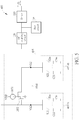
FIG. 5 is a diagram of anoscillator apparatus 400 according to a second embodiment of the invention. Theoscillator apparatus 400 can be a two-pin oscillator apparatus (not limited) and/or an on-chip oscillator apparatus (not limited). Theoscillator apparatus 400 is capable of reducing far-out phase noise as well as reducing closed-in phase noise. In practice, theoscillator apparatus 400 comprises anoscillator core circuit 405, thedriver 110, thebias circuit 115, and theDc coupling circuit 120 placed betweenoscillator core circuit 105 anddriver 110. Theoscillator core circuit 405 comprises thecurrent source 1051, the invertingtransconductance amplifier 1052 with negative transconductance gain -Gm, the first switchedcapacitor array 4053A, the second switchedcapacitor array 4053B, and theresonator 1054. The first switchedcapacitor array 4053A comprises a plurality of switches S11-S1n and a plurality of first capacitors with different/equal capacitances C11-Cln. The second switchedcapacitor array 4053B comprises a plurality of switches S21-S2m and a plurality of second capacitors with different/equal capacitances C21-C2m. Parameters n and m are positive integers and can be equal to each other or be different. Based on the switches S11-S1n and S21-S2m as well as capacitances C11-C1n and C21-C2m, theoscillator apparatus 400 can be used for providing an output signal with different oscillation frequencies. In addition, as shown inFIG. 5 , the invertingtransconductance amplifier 1052 can be implemented by using an NMOS transistor having a control node connected to the first port ofresonator 1054, a first node connected to thecurrent source 1052 and second port ofresonator 1054, and a second node connected to the ground level. - In addition, the inverting transconductance amplifier can be implemented by using COMS structure.
FIG. 6 is a diagram illustrating another implementation of theoscillator apparatus 400 as shown inFIG. 5 . The invertingtransconductance amplifier 1052 withinapparatus 400 is implemented by using complementary MOS structure circuit. The invertingtransconductance amplifier 1052 ofFIG. 6 comprises a NMOS transistor and a PMOS transistor. The PMOS transistor includes a control node connected to the first port ofresonator 1054, a first node connected to thecurrent source 1051, and a second node connected to the second port ofresonator 1054. The NMOS transistor includes a control node connected to the first port ofresonator 1054, a first node connected to the second port ofresonator 1054 and second node of the PMOS transistor, and a second node connected to the ground level. - Further, the
bias circuit 115 can be implemented by various kinds of circuits.FIG. 7 andFIG. 8 respectively illustrate different embodiments of thebias circuit 115 as shown inFIG. 1 . As shown inFIG. 7 , thebias circuit 115 comprises a resistor RB and aninverter 1151. The inverter size is selected according to consideration of low-noise and optimal bias point. The resistor RB is coupled between theDc coupling circuit 120 and theinverter 1151, and the resistor RB used as a high impedance/resistance to avoid noise loaded to theresonator 1054. Theinverter 1151 includes an input node coupled to the resistor RB and connected to its output node. Theinverter 1151 can be biased and controlled by a specific current provided from acurrent source 125 that is also used for providing the specific voltage to bias and control thedriver 110. Alternatively, as shown inFIG. 8 , thebias circuit 115 comprises the resistor RB that is connected between the input node ofdriver 110 and the output node ofdriver 110. These modifications all fall within the scope of the invention. - Furthermore, for the operation of the
oscillator apparatus 100/400, the upper bound limit of the ratio of C2 to C1 can be determined/calculated based on a frequency tuning range, load capacitance C_load, and the negative resistance -R specified above. In addition, the lower bound limit of the ratio of C2 to C1 is determined/calculated to avoid the active devices entering the triode region.
Claims (11)
- An oscillator apparatus (100), characterized by:an oscillator core circuit (105), comprising:an inverting transconductance amplifier (1052);at least one first capacitor (1053A, 4053A), connected between an input of the inverting transconductance amplifier (1052) and a ground level;at least one second capacitor (1053B, 4053B), connected between an output of the inverting transconductance amplifier (1052) and the ground level; anda resonator (1054), having a first port connected to the input of the inverting transconductance amplifier (1052) and a second port connected to the output of the inverting transconductance amplifier (1052), the first port being decoupled from the second port.
- The oscillator apparatus (100) of claim 1, characterized in that a DC voltage bias level at the first port is controlled not based on a DC voltage bias level at the second port.
- The oscillator apparatus (100) of claim 1, further characterized by:a DC coupling circuit (120), having one end connected to the input of the inverting transconductance amplifier (1052) and the first port and having another end connected to a driver (110); andthe driver (110), having an input DC coupled to the first port via the DC coupling circuit (120).
- The oscillator apparatus (100) of claim 1, further characterized by:a bias circuit (115), connected to the first port, configured to provide a common mode voltage level for a voltage signal at the first port.
- The oscillator apparatus (100) of claim 3, characterized in that the driver (110) comprises at least one of a squarer, an inverter buffer, and a voltage gain buffer.
- The oscillator apparatus (100) of claim 3, characterized in that the bias circuit (115) comprises:an inverter (1151), biased and controlled by a specific current of a current source (125), an output of the inverter (1151) being connected to an input of the inverter (1151); anda resistor (RB), connected between the first port of the resonator (1054) and the input of the inverter (1151);wherein the driver (110) is further biased by the specific current of the current source (125).
- The oscillator apparatus (100) of claim 3, characterized in that the bias circuit (115) comprises:a resistor (RB), having one end connected to an input of the driver (110) and another end connected to an output of the driver (110).
- The oscillator apparatus (100) of claim 1, characterized in that the at least one first capacitor (4053A) comprises a plurality of first capacitors (C11-C1n) connected in parallel and selectively coupled to the first port of the resonator (1054) via a plurality of first switches (S11-S1n) respectively; and, the at least one second capacitor (4053B) comprises a plurality of second capacitors (C21-C2m) connected in parallel and selectively coupled to the second port of the resonator (1054) via a plurality of second switches (S21-S2m) respectively.
- The oscillator apparatus (100) of claim 1, characterized in that a capacitance of the at least one first capacitor (1053A, 4053A) is smaller than a capacitance of the at least one second capacitor (1053B, 4053B).
- The oscillator apparatus (100) of claim 9, characterized in that an amplitude of a voltage signal at the first port of the resonator (1054) is larger than an amplitude of a voltage signal at the second port of the resonator (1054).
- The oscillator apparatus (100) of claim 9, characterized in that the at least one first capacitor (1053A, 4053A) is a linear capacitor, and the at least one second capacitor (1053B, 4053B) is a high density capacitor.
Applications Claiming Priority (2)
| Application Number | Priority Date | Filing Date | Title |
|---|---|---|---|
| US201562267296P | 2015-12-15 | 2015-12-15 | |
| US15/345,483 US10367450B2 (en) | 2015-12-15 | 2016-11-07 | Oscillator scheme capable of reducing far-out phase noise and closed-in phase noise |
Publications (3)
| Publication Number | Publication Date |
|---|---|
| EP3182583A2 true EP3182583A2 (en) | 2017-06-21 |
| EP3182583A3 EP3182583A3 (en) | 2017-09-06 |
| EP3182583B1 EP3182583B1 (en) | 2019-03-20 |
Family
ID=57288216
Family Applications (1)
| Application Number | Title | Priority Date | Filing Date |
|---|---|---|---|
| EP16198335.8A Active EP3182583B1 (en) | 2015-12-15 | 2016-11-11 | Oscillator scheme capable of reducing far-out phase noise and closed-in phase noise |
Country Status (3)
| Country | Link |
|---|---|
| US (1) | US10367450B2 (en) |
| EP (1) | EP3182583B1 (en) |
| CN (1) | CN107070405B (en) |
Families Citing this family (6)
| Publication number | Priority date | Publication date | Assignee | Title |
|---|---|---|---|---|
| JP6843605B2 (en) * | 2016-12-06 | 2021-03-17 | キヤノン株式会社 | Power supply and image forming equipment |
| US11309835B2 (en) | 2020-08-26 | 2022-04-19 | Mediatek Inc. | Crystal oscillator and phase noise reduction method thereof |
| US11342884B2 (en) | 2020-08-26 | 2022-05-24 | Mediatek Inc. | Crystal oscillator and phase noise reduction method thereof |
| US11837995B2 (en) * | 2021-05-25 | 2023-12-05 | Mediatek Inc. | One-coil multi-core inductor-capacitor oscillator |
| KR20250016686A (en) * | 2023-07-24 | 2025-02-04 | 삼성디스플레이 주식회사 | Electronic device |
| CN118330323A (en) * | 2024-06-13 | 2024-07-12 | 天津伍嘉联创科技发展股份有限公司 | A test circuit for measuring electrical parameters of tuning fork quartz resonator crystal |
Family Cites Families (17)
| Publication number | Priority date | Publication date | Assignee | Title |
|---|---|---|---|---|
| US3829795A (en) | 1971-08-13 | 1974-08-13 | Rockwell International Corp | Crystal oscillator using field effect transistors in an integrated circuit |
| JP2716869B2 (en) | 1990-11-29 | 1998-02-18 | 株式会社東芝 | Oscillation circuit |
| JP2985489B2 (en) | 1992-03-31 | 1999-11-29 | 日本電気株式会社 | Phase locked loop |
| US5757242A (en) * | 1996-12-09 | 1998-05-26 | Industrial Technology Research Institute | Low power consumption oscillators with output level shifters |
| US6798301B1 (en) | 2001-06-11 | 2004-09-28 | Lsi Logic Corporation | Method and apparatus for controlling oscillation amplitude and oscillation frequency of crystal oscillator |
| JP3877597B2 (en) | 2002-01-21 | 2007-02-07 | シャープ株式会社 | Multi-terminal MOS varactor |
| KR100551477B1 (en) | 2004-02-20 | 2006-02-14 | 삼성전자주식회사 | Capacitor Bank Circuits and Voltage Controlled Oscillators |
| US7123113B1 (en) * | 2004-06-11 | 2006-10-17 | Cypress Semiconductor Corp. | Regulated, symmetrical crystal oscillator circuit and method |
| US7289003B2 (en) | 2005-08-03 | 2007-10-30 | Seiko Epson Corporation | Method and apparatus for amplitude control using dynamic biasing in a voltage controlled oscillator |
| JP5027472B2 (en) | 2005-11-09 | 2012-09-19 | ルネサスエレクトロニクス株式会社 | Oscillator and information device using the same |
| EP1916762B1 (en) | 2006-10-27 | 2018-05-30 | EM Microelectronic-Marin SA | Quartz oscillator with amplitude control and an extended temperature range. |
| EP2073377A1 (en) | 2007-12-19 | 2009-06-24 | The Swatch Group Research and Development Ltd. | Oscillating quartz circuit with low consumption and active biasing |
| US8773215B2 (en) | 2011-09-09 | 2014-07-08 | International Business Machines Corporation | Fully decoupled LC-tank based oscillator topology for low phase noise and high oscillation amplitude applications |
| JP2015088930A (en) | 2013-10-30 | 2015-05-07 | セイコーエプソン株式会社 | Oscillation circuit, oscillator, method of manufacturing oscillator, electronic apparatus, and moving body |
| JP2015104074A (en) | 2013-11-27 | 2015-06-04 | セイコーエプソン株式会社 | Oscillator circuit, oscillator, electronic device and mobile object |
| US10135390B2 (en) * | 2015-06-22 | 2018-11-20 | Microchip Technology Incorporated | Periodic kick-starter for a crystal oscillator |
| US9647670B2 (en) * | 2015-09-15 | 2017-05-09 | Silicon Laboratories Inc. | Oscillator with dynamic gain control |
-
2016
- 2016-11-07 US US15/345,483 patent/US10367450B2/en active Active
- 2016-11-11 EP EP16198335.8A patent/EP3182583B1/en active Active
- 2016-12-15 CN CN201611158495.6A patent/CN107070405B/en active Active
Non-Patent Citations (1)
| Title |
|---|
| None |
Also Published As
| Publication number | Publication date |
|---|---|
| EP3182583A3 (en) | 2017-09-06 |
| CN107070405B (en) | 2020-12-18 |
| CN107070405A (en) | 2017-08-18 |
| US20170170784A1 (en) | 2017-06-15 |
| US10367450B2 (en) | 2019-07-30 |
| EP3182583B1 (en) | 2019-03-20 |
Similar Documents
| Publication | Publication Date | Title |
|---|---|---|
| EP3182583B1 (en) | Oscillator scheme capable of reducing far-out phase noise and closed-in phase noise | |
| CN101682293B (en) | Voltage controlled oscillator, and pll circuit and wireless communication device using voltage controlled oscillator | |
| JP2009284329A (en) | Semiconductor integrated circuit device | |
| US9013234B2 (en) | Transconductance adjustment circuit, circuit device, and electronic apparatus | |
| JP4358185B2 (en) | Voltage-controlled oscillator, transmitter and receiver | |
| US6882216B2 (en) | On-chip high-pass filter with large time constant | |
| KR101855037B1 (en) | Sub-nyquist receiver of using pseudo random binary sequence generator | |
| US20220263464A1 (en) | Oscillator circuit and device | |
| US20080164954A1 (en) | Voltage controlled oscillator for controlling phase noise and method using the same | |
| JP4776928B2 (en) | Frequency multiplier | |
| US7456697B2 (en) | Variable degeneration impedance supply circuit using switch and electronic circuits using the same | |
| US8274320B2 (en) | Signal processing circuit with improved linearity | |
| US7847585B2 (en) | Source follower with active inductance as a load | |
| US20060176121A1 (en) | Piezoelectric oscillator having symmetric inverter pair | |
| JP2006060797A (en) | Voltage controlled oscillator | |
| US10305427B2 (en) | Digital modulating device, frequency doubling modulator thereof and frequency doubler | |
| EP1703632A1 (en) | Piezoelectric oscillator | |
| US10483912B1 (en) | Non-inverting multi-mode oscillator | |
| KR100538614B1 (en) | Voltage control oscillator | |
| JP2006019938A (en) | Voltage controlled oscillator and wireless communication device | |
| KR20020032424A (en) | Resonator | |
| US9287860B2 (en) | Negative resistance generator, load including negative resistance and load of amplifier | |
| JP2007096779A (en) | Semiconductor device | |
| JPWO2008111187A1 (en) | Oscillator and semiconductor device | |
| JP2007274649A (en) | Oscillator circuit |
Legal Events
| Date | Code | Title | Description |
|---|---|---|---|
| PUAI | Public reference made under article 153(3) epc to a published international application that has entered the european phase |
Free format text: ORIGINAL CODE: 0009012 |
|
| STAA | Information on the status of an ep patent application or granted ep patent |
Free format text: STATUS: THE APPLICATION HAS BEEN PUBLISHED |
|
| AK | Designated contracting states |
Kind code of ref document: A2 Designated state(s): AL AT BE BG CH CY CZ DE DK EE ES FI FR GB GR HR HU IE IS IT LI LT LU LV MC MK MT NL NO PL PT RO RS SE SI SK SM TR |
|
| AX | Request for extension of the european patent |
Extension state: BA ME |
|
| PUAL | Search report despatched |
Free format text: ORIGINAL CODE: 0009013 |
|
| AK | Designated contracting states |
Kind code of ref document: A3 Designated state(s): AL AT BE BG CH CY CZ DE DK EE ES FI FR GB GR HR HU IE IS IT LI LT LU LV MC MK MT NL NO PL PT RO RS SE SI SK SM TR |
|
| AX | Request for extension of the european patent |
Extension state: BA ME |
|
| RIC1 | Information provided on ipc code assigned before grant |
Ipc: H03B 5/36 20060101AFI20170728BHEP Ipc: H03B 1/04 20060101ALI20170728BHEP |
|
| STAA | Information on the status of an ep patent application or granted ep patent |
Free format text: STATUS: REQUEST FOR EXAMINATION WAS MADE |
|
| 17P | Request for examination filed |
Effective date: 20180305 |
|
| RBV | Designated contracting states (corrected) |
Designated state(s): AL AT BE BG CH CY CZ DE DK EE ES FI FR GB GR HR HU IE IS IT LI LT LU LV MC MK MT NL NO PL PT RO RS SE SI SK SM TR |
|
| GRAP | Despatch of communication of intention to grant a patent |
Free format text: ORIGINAL CODE: EPIDOSNIGR1 |
|
| STAA | Information on the status of an ep patent application or granted ep patent |
Free format text: STATUS: GRANT OF PATENT IS INTENDED |
|
| INTG | Intention to grant announced |
Effective date: 20181213 |
|
| GRAS | Grant fee paid |
Free format text: ORIGINAL CODE: EPIDOSNIGR3 |
|
| GRAA | (expected) grant |
Free format text: ORIGINAL CODE: 0009210 |
|
| STAA | Information on the status of an ep patent application or granted ep patent |
Free format text: STATUS: THE PATENT HAS BEEN GRANTED |
|
| AK | Designated contracting states |
Kind code of ref document: B1 Designated state(s): AL AT BE BG CH CY CZ DE DK EE ES FI FR GB GR HR HU IE IS IT LI LT LU LV MC MK MT NL NO PL PT RO RS SE SI SK SM TR |
|
| REG | Reference to a national code |
Ref country code: GB Ref legal event code: FG4D |
|
| REG | Reference to a national code |
Ref country code: CH Ref legal event code: EP |
|
| REG | Reference to a national code |
Ref country code: DE Ref legal event code: R096 Ref document number: 602016011242 Country of ref document: DE |
|
| REG | Reference to a national code |
Ref country code: AT Ref legal event code: REF Ref document number: 1111549 Country of ref document: AT Kind code of ref document: T Effective date: 20190415 |
|
| REG | Reference to a national code |
Ref country code: IE Ref legal event code: FG4D |
|
| REG | Reference to a national code |
Ref country code: NL Ref legal event code: MP Effective date: 20190320 |
|
| PG25 | Lapsed in a contracting state [announced via postgrant information from national office to epo] |
Ref country code: SE Free format text: LAPSE BECAUSE OF FAILURE TO SUBMIT A TRANSLATION OF THE DESCRIPTION OR TO PAY THE FEE WITHIN THE PRESCRIBED TIME-LIMIT Effective date: 20190320 Ref country code: FI Free format text: LAPSE BECAUSE OF FAILURE TO SUBMIT A TRANSLATION OF THE DESCRIPTION OR TO PAY THE FEE WITHIN THE PRESCRIBED TIME-LIMIT Effective date: 20190320 Ref country code: NO Free format text: LAPSE BECAUSE OF FAILURE TO SUBMIT A TRANSLATION OF THE DESCRIPTION OR TO PAY THE FEE WITHIN THE PRESCRIBED TIME-LIMIT Effective date: 20190620 Ref country code: LT Free format text: LAPSE BECAUSE OF FAILURE TO SUBMIT A TRANSLATION OF THE DESCRIPTION OR TO PAY THE FEE WITHIN THE PRESCRIBED TIME-LIMIT Effective date: 20190320 |
|
| REG | Reference to a national code |
Ref country code: LT Ref legal event code: MG4D |
|
| PG25 | Lapsed in a contracting state [announced via postgrant information from national office to epo] |
Ref country code: GR Free format text: LAPSE BECAUSE OF FAILURE TO SUBMIT A TRANSLATION OF THE DESCRIPTION OR TO PAY THE FEE WITHIN THE PRESCRIBED TIME-LIMIT Effective date: 20190621 Ref country code: HR Free format text: LAPSE BECAUSE OF FAILURE TO SUBMIT A TRANSLATION OF THE DESCRIPTION OR TO PAY THE FEE WITHIN THE PRESCRIBED TIME-LIMIT Effective date: 20190320 Ref country code: LV Free format text: LAPSE BECAUSE OF FAILURE TO SUBMIT A TRANSLATION OF THE DESCRIPTION OR TO PAY THE FEE WITHIN THE PRESCRIBED TIME-LIMIT Effective date: 20190320 Ref country code: NL Free format text: LAPSE BECAUSE OF FAILURE TO SUBMIT A TRANSLATION OF THE DESCRIPTION OR TO PAY THE FEE WITHIN THE PRESCRIBED TIME-LIMIT Effective date: 20190320 Ref country code: RS Free format text: LAPSE BECAUSE OF FAILURE TO SUBMIT A TRANSLATION OF THE DESCRIPTION OR TO PAY THE FEE WITHIN THE PRESCRIBED TIME-LIMIT Effective date: 20190320 Ref country code: BG Free format text: LAPSE BECAUSE OF FAILURE TO SUBMIT A TRANSLATION OF THE DESCRIPTION OR TO PAY THE FEE WITHIN THE PRESCRIBED TIME-LIMIT Effective date: 20190620 |
|
| REG | Reference to a national code |
Ref country code: AT Ref legal event code: MK05 Ref document number: 1111549 Country of ref document: AT Kind code of ref document: T Effective date: 20190320 |
|
| PG25 | Lapsed in a contracting state [announced via postgrant information from national office to epo] |
Ref country code: CZ Free format text: LAPSE BECAUSE OF FAILURE TO SUBMIT A TRANSLATION OF THE DESCRIPTION OR TO PAY THE FEE WITHIN THE PRESCRIBED TIME-LIMIT Effective date: 20190320 Ref country code: IT Free format text: LAPSE BECAUSE OF FAILURE TO SUBMIT A TRANSLATION OF THE DESCRIPTION OR TO PAY THE FEE WITHIN THE PRESCRIBED TIME-LIMIT Effective date: 20190320 Ref country code: ES Free format text: LAPSE BECAUSE OF FAILURE TO SUBMIT A TRANSLATION OF THE DESCRIPTION OR TO PAY THE FEE WITHIN THE PRESCRIBED TIME-LIMIT Effective date: 20190320 Ref country code: RO Free format text: LAPSE BECAUSE OF FAILURE TO SUBMIT A TRANSLATION OF THE DESCRIPTION OR TO PAY THE FEE WITHIN THE PRESCRIBED TIME-LIMIT Effective date: 20190320 Ref country code: EE Free format text: LAPSE BECAUSE OF FAILURE TO SUBMIT A TRANSLATION OF THE DESCRIPTION OR TO PAY THE FEE WITHIN THE PRESCRIBED TIME-LIMIT Effective date: 20190320 Ref country code: AL Free format text: LAPSE BECAUSE OF FAILURE TO SUBMIT A TRANSLATION OF THE DESCRIPTION OR TO PAY THE FEE WITHIN THE PRESCRIBED TIME-LIMIT Effective date: 20190320 Ref country code: PT Free format text: LAPSE BECAUSE OF FAILURE TO SUBMIT A TRANSLATION OF THE DESCRIPTION OR TO PAY THE FEE WITHIN THE PRESCRIBED TIME-LIMIT Effective date: 20190720 Ref country code: SK Free format text: LAPSE BECAUSE OF FAILURE TO SUBMIT A TRANSLATION OF THE DESCRIPTION OR TO PAY THE FEE WITHIN THE PRESCRIBED TIME-LIMIT Effective date: 20190320 |
|
| PG25 | Lapsed in a contracting state [announced via postgrant information from national office to epo] |
Ref country code: PL Free format text: LAPSE BECAUSE OF FAILURE TO SUBMIT A TRANSLATION OF THE DESCRIPTION OR TO PAY THE FEE WITHIN THE PRESCRIBED TIME-LIMIT Effective date: 20190320 Ref country code: SM Free format text: LAPSE BECAUSE OF FAILURE TO SUBMIT A TRANSLATION OF THE DESCRIPTION OR TO PAY THE FEE WITHIN THE PRESCRIBED TIME-LIMIT Effective date: 20190320 |
|
| PG25 | Lapsed in a contracting state [announced via postgrant information from national office to epo] |
Ref country code: AT Free format text: LAPSE BECAUSE OF FAILURE TO SUBMIT A TRANSLATION OF THE DESCRIPTION OR TO PAY THE FEE WITHIN THE PRESCRIBED TIME-LIMIT Effective date: 20190320 Ref country code: IS Free format text: LAPSE BECAUSE OF FAILURE TO SUBMIT A TRANSLATION OF THE DESCRIPTION OR TO PAY THE FEE WITHIN THE PRESCRIBED TIME-LIMIT Effective date: 20190720 |
|
| REG | Reference to a national code |
Ref country code: DE Ref legal event code: R097 Ref document number: 602016011242 Country of ref document: DE |
|
| PLBE | No opposition filed within time limit |
Free format text: ORIGINAL CODE: 0009261 |
|
| STAA | Information on the status of an ep patent application or granted ep patent |
Free format text: STATUS: NO OPPOSITION FILED WITHIN TIME LIMIT |
|
| PG25 | Lapsed in a contracting state [announced via postgrant information from national office to epo] |
Ref country code: DK Free format text: LAPSE BECAUSE OF FAILURE TO SUBMIT A TRANSLATION OF THE DESCRIPTION OR TO PAY THE FEE WITHIN THE PRESCRIBED TIME-LIMIT Effective date: 20190320 |
|
| 26N | No opposition filed |
Effective date: 20200102 |
|
| PG25 | Lapsed in a contracting state [announced via postgrant information from national office to epo] |
Ref country code: SI Free format text: LAPSE BECAUSE OF FAILURE TO SUBMIT A TRANSLATION OF THE DESCRIPTION OR TO PAY THE FEE WITHIN THE PRESCRIBED TIME-LIMIT Effective date: 20190320 |
|
| PG25 | Lapsed in a contracting state [announced via postgrant information from national office to epo] |
Ref country code: TR Free format text: LAPSE BECAUSE OF FAILURE TO SUBMIT A TRANSLATION OF THE DESCRIPTION OR TO PAY THE FEE WITHIN THE PRESCRIBED TIME-LIMIT Effective date: 20190320 |
|
| REG | Reference to a national code |
Ref country code: CH Ref legal event code: PL |
|
| PG25 | Lapsed in a contracting state [announced via postgrant information from national office to epo] |
Ref country code: CH Free format text: LAPSE BECAUSE OF NON-PAYMENT OF DUE FEES Effective date: 20191130 Ref country code: LU Free format text: LAPSE BECAUSE OF NON-PAYMENT OF DUE FEES Effective date: 20191111 Ref country code: MC Free format text: LAPSE BECAUSE OF FAILURE TO SUBMIT A TRANSLATION OF THE DESCRIPTION OR TO PAY THE FEE WITHIN THE PRESCRIBED TIME-LIMIT Effective date: 20190320 Ref country code: LI Free format text: LAPSE BECAUSE OF NON-PAYMENT OF DUE FEES Effective date: 20191130 |
|
| REG | Reference to a national code |
Ref country code: BE Ref legal event code: MM Effective date: 20191130 |
|
| PG25 | Lapsed in a contracting state [announced via postgrant information from national office to epo] |
Ref country code: IE Free format text: LAPSE BECAUSE OF NON-PAYMENT OF DUE FEES Effective date: 20191111 |
|
| PG25 | Lapsed in a contracting state [announced via postgrant information from national office to epo] |
Ref country code: BE Free format text: LAPSE BECAUSE OF NON-PAYMENT OF DUE FEES Effective date: 20191130 |
|
| PG25 | Lapsed in a contracting state [announced via postgrant information from national office to epo] |
Ref country code: CY Free format text: LAPSE BECAUSE OF FAILURE TO SUBMIT A TRANSLATION OF THE DESCRIPTION OR TO PAY THE FEE WITHIN THE PRESCRIBED TIME-LIMIT Effective date: 20190320 |
|
| PG25 | Lapsed in a contracting state [announced via postgrant information from national office to epo] |
Ref country code: HU Free format text: LAPSE BECAUSE OF FAILURE TO SUBMIT A TRANSLATION OF THE DESCRIPTION OR TO PAY THE FEE WITHIN THE PRESCRIBED TIME-LIMIT; INVALID AB INITIO Effective date: 20161111 Ref country code: MT Free format text: LAPSE BECAUSE OF FAILURE TO SUBMIT A TRANSLATION OF THE DESCRIPTION OR TO PAY THE FEE WITHIN THE PRESCRIBED TIME-LIMIT Effective date: 20190320 |
|
| PG25 | Lapsed in a contracting state [announced via postgrant information from national office to epo] |
Ref country code: MK Free format text: LAPSE BECAUSE OF FAILURE TO SUBMIT A TRANSLATION OF THE DESCRIPTION OR TO PAY THE FEE WITHIN THE PRESCRIBED TIME-LIMIT Effective date: 20190320 |
|
| P01 | Opt-out of the competence of the unified patent court (upc) registered |
Effective date: 20230607 |
|
| PGFP | Annual fee paid to national office [announced via postgrant information from national office to epo] |
Ref country code: GB Payment date: 20250918 Year of fee payment: 10 |
|
| PGFP | Annual fee paid to national office [announced via postgrant information from national office to epo] |
Ref country code: FR Payment date: 20250908 Year of fee payment: 10 |
|
| PGFP | Annual fee paid to national office [announced via postgrant information from national office to epo] |
Ref country code: DE Payment date: 20250916 Year of fee payment: 10 |