EP3182573A1 - Snubber circuits adapted to limit energy leaking from two terminals of a winding and electronic circuit - Google Patents
Snubber circuits adapted to limit energy leaking from two terminals of a winding and electronic circuit Download PDFInfo
- Publication number
- EP3182573A1 EP3182573A1 EP15306998.4A EP15306998A EP3182573A1 EP 3182573 A1 EP3182573 A1 EP 3182573A1 EP 15306998 A EP15306998 A EP 15306998A EP 3182573 A1 EP3182573 A1 EP 3182573A1
- Authority
- EP
- European Patent Office
- Prior art keywords
- rectifier
- capacitor
- terminal
- snubber circuit
- winding
- Prior art date
- Legal status (The legal status is an assumption and is not a legal conclusion. Google has not performed a legal analysis and makes no representation as to the accuracy of the status listed.)
- Withdrawn
Links
- 238000004804 winding Methods 0.000 title claims abstract description 26
- 239000003990 capacitor Substances 0.000 claims abstract description 48
- XUIMIQQOPSSXEZ-UHFFFAOYSA-N Silicon Chemical compound [Si] XUIMIQQOPSSXEZ-UHFFFAOYSA-N 0.000 claims description 9
- 230000005669 field effect Effects 0.000 claims description 4
- 239000003985 ceramic capacitor Substances 0.000 claims description 2
- 238000005259 measurement Methods 0.000 description 8
- 230000000903 blocking effect Effects 0.000 description 3
- 230000010355 oscillation Effects 0.000 description 2
- 230000003071 parasitic effect Effects 0.000 description 2
- 241000656145 Thyrsites atun Species 0.000 description 1
- 230000001010 compromised effect Effects 0.000 description 1
- 239000004020 conductor Substances 0.000 description 1
- 238000013016 damping Methods 0.000 description 1
- 230000000694 effects Effects 0.000 description 1
- 238000000034 method Methods 0.000 description 1
- 238000011084 recovery Methods 0.000 description 1
- 229910052710 silicon Inorganic materials 0.000 description 1
- 239000010703 silicon Substances 0.000 description 1
Images



Classifications
-
- H—ELECTRICITY
- H02—GENERATION; CONVERSION OR DISTRIBUTION OF ELECTRIC POWER
- H02M—APPARATUS FOR CONVERSION BETWEEN AC AND AC, BETWEEN AC AND DC, OR BETWEEN DC AND DC, AND FOR USE WITH MAINS OR SIMILAR POWER SUPPLY SYSTEMS; CONVERSION OF DC OR AC INPUT POWER INTO SURGE OUTPUT POWER; CONTROL OR REGULATION THEREOF
- H02M1/00—Details of apparatus for conversion
- H02M1/32—Means for protecting converters other than automatic disconnection
- H02M1/34—Snubber circuits
-
- H—ELECTRICITY
- H02—GENERATION; CONVERSION OR DISTRIBUTION OF ELECTRIC POWER
- H02M—APPARATUS FOR CONVERSION BETWEEN AC AND AC, BETWEEN AC AND DC, OR BETWEEN DC AND DC, AND FOR USE WITH MAINS OR SIMILAR POWER SUPPLY SYSTEMS; CONVERSION OF DC OR AC INPUT POWER INTO SURGE OUTPUT POWER; CONTROL OR REGULATION THEREOF
- H02M1/00—Details of apparatus for conversion
- H02M1/32—Means for protecting converters other than automatic disconnection
- H02M1/34—Snubber circuits
- H02M1/346—Passive non-dissipative snubbers
-
- H—ELECTRICITY
- H02—GENERATION; CONVERSION OR DISTRIBUTION OF ELECTRIC POWER
- H02M—APPARATUS FOR CONVERSION BETWEEN AC AND AC, BETWEEN AC AND DC, OR BETWEEN DC AND DC, AND FOR USE WITH MAINS OR SIMILAR POWER SUPPLY SYSTEMS; CONVERSION OF DC OR AC INPUT POWER INTO SURGE OUTPUT POWER; CONTROL OR REGULATION THEREOF
- H02M1/00—Details of apparatus for conversion
- H02M1/32—Means for protecting converters other than automatic disconnection
- H02M1/34—Snubber circuits
- H02M1/348—Passive dissipative snubbers
-
- H—ELECTRICITY
- H02—GENERATION; CONVERSION OR DISTRIBUTION OF ELECTRIC POWER
- H02M—APPARATUS FOR CONVERSION BETWEEN AC AND AC, BETWEEN AC AND DC, OR BETWEEN DC AND DC, AND FOR USE WITH MAINS OR SIMILAR POWER SUPPLY SYSTEMS; CONVERSION OF DC OR AC INPUT POWER INTO SURGE OUTPUT POWER; CONTROL OR REGULATION THEREOF
- H02M3/00—Conversion of DC power input into DC power output
- H02M3/22—Conversion of DC power input into DC power output with intermediate conversion into AC
- H02M3/24—Conversion of DC power input into DC power output with intermediate conversion into AC by static converters
- H02M3/28—Conversion of DC power input into DC power output with intermediate conversion into AC by static converters using discharge tubes with control electrode or semiconductor devices with control electrode to produce the intermediate AC
- H02M3/325—Conversion of DC power input into DC power output with intermediate conversion into AC by static converters using discharge tubes with control electrode or semiconductor devices with control electrode to produce the intermediate AC using devices of a triode or a transistor type requiring continuous application of a control signal
- H02M3/335—Conversion of DC power input into DC power output with intermediate conversion into AC by static converters using discharge tubes with control electrode or semiconductor devices with control electrode to produce the intermediate AC using devices of a triode or a transistor type requiring continuous application of a control signal using semiconductor devices only
-
- H—ELECTRICITY
- H02—GENERATION; CONVERSION OR DISTRIBUTION OF ELECTRIC POWER
- H02M—APPARATUS FOR CONVERSION BETWEEN AC AND AC, BETWEEN AC AND DC, OR BETWEEN DC AND DC, AND FOR USE WITH MAINS OR SIMILAR POWER SUPPLY SYSTEMS; CONVERSION OF DC OR AC INPUT POWER INTO SURGE OUTPUT POWER; CONTROL OR REGULATION THEREOF
- H02M3/00—Conversion of DC power input into DC power output
- H02M3/22—Conversion of DC power input into DC power output with intermediate conversion into AC
- H02M3/24—Conversion of DC power input into DC power output with intermediate conversion into AC by static converters
- H02M3/28—Conversion of DC power input into DC power output with intermediate conversion into AC by static converters using discharge tubes with control electrode or semiconductor devices with control electrode to produce the intermediate AC
- H02M3/325—Conversion of DC power input into DC power output with intermediate conversion into AC by static converters using discharge tubes with control electrode or semiconductor devices with control electrode to produce the intermediate AC using devices of a triode or a transistor type requiring continuous application of a control signal
- H02M3/335—Conversion of DC power input into DC power output with intermediate conversion into AC by static converters using discharge tubes with control electrode or semiconductor devices with control electrode to produce the intermediate AC using devices of a triode or a transistor type requiring continuous application of a control signal using semiconductor devices only
- H02M3/33538—Conversion of DC power input into DC power output with intermediate conversion into AC by static converters using discharge tubes with control electrode or semiconductor devices with control electrode to produce the intermediate AC using devices of a triode or a transistor type requiring continuous application of a control signal using semiconductor devices only of the forward type
-
- Y—GENERAL TAGGING OF NEW TECHNOLOGICAL DEVELOPMENTS; GENERAL TAGGING OF CROSS-SECTIONAL TECHNOLOGIES SPANNING OVER SEVERAL SECTIONS OF THE IPC; TECHNICAL SUBJECTS COVERED BY FORMER USPC CROSS-REFERENCE ART COLLECTIONS [XRACs] AND DIGESTS
- Y02—TECHNOLOGIES OR APPLICATIONS FOR MITIGATION OR ADAPTATION AGAINST CLIMATE CHANGE
- Y02B—CLIMATE CHANGE MITIGATION TECHNOLOGIES RELATED TO BUILDINGS, e.g. HOUSING, HOUSE APPLIANCES OR RELATED END-USER APPLICATIONS
- Y02B70/00—Technologies for an efficient end-user side electric power management and consumption
- Y02B70/10—Technologies improving the efficiency by using switched-mode power supplies [SMPS], i.e. efficient power electronics conversion e.g. power factor correction or reduction of losses in power supplies or efficient standby modes
Definitions
- the present subject matter relates to snubber circuit integrated for example within an inverting boost converter with coupled inductor.
- the principle of the present subject matter may be adapted to other types of switch mode converters, for example forward or flyback.
- transformers or coupled inductor based switch mode power supply has to deal with not-ideal components like transformers or coupled inductors. Among other things the later show more or less primary and secondary side leakage inductance. In switching applications these unwanted parasitic inductances can generate significant spikes and ringing at the primary and secondary side switch nodes.
- the developer has to take care for this and usually needs to implement snubber circuitry to limit the negative effects of spikes and ringing which are stress of components and most likely Electromagnetic compatibility (EMC) issues.
- EMC Electromagnetic compatibility
- R-C snubber circuit presented figure 1-a
- R-C-D snubber circuits presented figure 1-b and figure 1-c .
- These snubber circuits are feasible and often used but highly dissipative, which heavily can degrade the efficiency of the whole circuitry.
- a snubber circuit is described.
- the snubber circuit is adapted to limit energy leaking from a first terminal and a second terminal of a winding, the snubber circuit comprising a first rectifier and a second rectifier and a third rectifier and a first capacitor and a second capacitor.
- a cathode of first rectifier is connected to the first terminal.
- an anode of the first rectifier is connected to a cathode of the second rectifier.
- an anode of the third rectifier is connected to anode of the second rectifier.
- a cathode of the third rectifier is connected to the second terminal and to a first terminal of the first capacitor.
- a second terminal of the first capacitor is connected to the anode of the first rectifier.
- a first terminal of the second capacitor is connected to the first terminal of the winding and a second terminal of the second capacitor is connected to the anode of the third rectifier.
- an electronic circuit comprising a snubber circuit connected to two terminals of the winding.
- the snubber circuit is adapted to limit energy leaking from a first terminal and a second terminal of a winding, the snubber circuit comprising a first rectifier and a second rectifier and a third rectifier and a first capacitor and a second capacitor.
- a cathode of first rectifier is connected to the first terminal.
- an anode of the first rectifier is connected to a cathode of the second rectifier.
- an anode of the third rectifier is connected to anode of the second rectifier.
- a cathode of the third rectifier is connected to the second terminal and to a first terminal of the first capacitor.
- a second terminal of the first capacitor is connected to the anode of the first rectifier.
- a first terminal of the second capacitor is connected to the first terminal of the winding and a second terminal of the second capacitor is connected to the anode of the third rectifier
- An embodiment of the present subject matter is a snubber circuit.
- This snubber circuit is adapted to limit energy leaking from two terminals of a winding.
- winding we mean a circuit comprising a wire or a conductor which constitutes a coil.
- the circuitry with bothersome leakage is a converter with two sides, so called primary and secondary side. Each side is galvanically isolated of each other by use of a transformer or a coupled inductor. These components present the unwanted leakage inductances.
- a non-isolated type e.g. a buck or step down converter. But here we don't have this type of leakage but only much lower parasitic inductances caused by e.g. the layout.
- Figure 2 presents an snubber circuit of the present subject matter.
- This snubber circuit is adapted to limit energy leaking from a first terminal and a second terminal of a winding 201.
- the snubber circuit comprises
- the rectifier D3 can be obtain via different type of elements, for example diodes or field effect transistors (FET).
- the field effect transistor is more complex (additional driver circuitry is needed) but can increase system efficiency a lot. Especially for low output voltages (the diode losses are avoided).
- the rectifier is a diode it could be for example silicium fast switching diode or a Schottky diode. The choice between these two types of diode depends on required blocking voltage. In all case the diode needs to be of fast diode type and capable to handle the output current for short periods.
- the rectifiers D1 or D2 could be a diode for example silicium fast switching diode or a Schottky diode.
- the first rectifier D1 is a fast switching silicium diode or a Schottky diode and/or the second rectifier D2 is a fast switching silicium diode or a Schottky diode and/or the third rectifier D3 is a fast switching silicium diode or a Schottky diode or a field effect transistor.
- the first capacitor C1 is a film capacitor or a ceramic capacitor.
- the capacitors, of the present subject matter need to be a low ESR type and to be capable of handling pulse currents.
- the capacitor C1 likely has a capacity in the nF (nano farad) range.
- C 1 is the capacity of the first capacitor and I 0 is the maximum output current of the winding (202) and dUC the wanted first capacitor (C1) voltage and L 1 is the leakage inductance of a coupled inductor of the winding (202).
- the value of this capacity must be finely tune by performing try and error.
- the figure 3 presents another embodiment of the present subject matter.
- the first terminal of the first capacitor C1 is connected to the cathode of the third diode D3 via a resistance R.
- the resistance R is below 10 Ohm.
- the exact value of this resistance depends on what the expected performance of the snubber circuit, more precisely how much damping of remaining oscillation is wanted at the cost of efficiency loss.
- the value of the resistance R could be 1 ohm.
- the winding comprises a coupled inductor, the coupled inductor comprising a first and a second side and a switch configured to applied a voltage across the primary side of the coupled inductor when the switch is turn on, and wherein the snubber circuit is connected to the second side of the coupled inductor.
- the dots closed to the coupled inductor represent the starting point of each winding. It is presupposed that the winding directions are identical. So this is also indication of voltage polarities that establish.
- the embodiments of the present subject matter heavily reduce spikes and ringing at the secondary side switch node. Furthermore the circuit efficiency is almost not compromised. Also these snubber circuits add only a minimal additional expenses indeed there is only two diodes plus a capacitor to add. Furthermore to the reduced peak to peak voltage a lower voltage rectifier diode could be used. This further could increase the total circuit efficiency and/or reduce costs.
- the figure 5, 6 and 7 present different measurements made using some of the circuits of the present divulgation.
- the input voltage is 5V
- the output voltage is -52V
- the output current is 0.6A
- the switching frequency is about 450kHz.
- the figure 5 is a measurement made when no snubber circuit is used. This measurement presents high voltage spikes and heavy ringing.
- the diode D1 and D2 are BAS16H (silicon switching diode, case SOD-323, 100V, 6ns). In comparison with the measurement of figure 5 , the voltage spikes are heavily reduced and ringing is damped.
- the figure 7 presents the comparison of the efficiency of an inverting boost converter with snubber circuit according to figure 4 , measurement with the triangles, and an inverting boost converter without snubber circuit, measurement with the circles. This figure 7 highlights that there is no decrease of efficiency with the proposed snubber circuit of figure.
- the figure 8 presents another embodiment of the present subject matter.
- the snubber circuit is of the type non-inverting boost converter or isolated flyback.
- the figure 9 presents another embodiment of the present subject matter.
- the snubber circuit is of the type forward converter.
Landscapes
- Engineering & Computer Science (AREA)
- Power Engineering (AREA)
- Dc-Dc Converters (AREA)
Abstract
Snubber circuit is adapted to limit energy leaking from a first terminal and a second terminal of a winding, and electronic circuit the snubber circuit comprising a first rectifier and a second rectifier and a third rectifier and a first capacitor and a second capacitor. Within the snubber circuit a cathode of first rectifier is connected to the first terminal. Within the snubber circuit an anode of the first rectifier is connected to a cathode of the second rectifier. Within the snubber circuit an anode of the third rectifier is connected to anode of the second rectifier. Within the snubber circuit a cathode of the third rectifier is connected to the second terminal and to a first terminal of the first capacitor. Within the snubber circuit a second terminal of the first capacitor is connected to the anode of the first rectifier. Within the snubber circuit a first terminal of the second capacitor is connected to the first terminal of the winding and a second terminal of the second capacitor is connected to the anode of the third rectifier.
Description
- The present subject matter relates to snubber circuit integrated for example within an inverting boost converter with coupled inductor. However the principle of the present subject matter may be adapted to other types of switch mode converters, for example forward or flyback.
- Any transformer or coupled inductor based switch mode power supply has to deal with not-ideal components like transformers or coupled inductors. Among other things the later show more or less primary and secondary side leakage inductance. In switching applications these unwanted parasitic inductances can generate significant spikes and ringing at the primary and secondary side switch nodes.
- The developer has to take care for this and usually needs to implement snubber circuitry to limit the negative effects of spikes and ringing which are stress of components and most likely Electromagnetic compatibility (EMC) issues.
- For primary side snubbers low-loss circuitry (e.g. active clamp) is known but not for secondary side ones.
- Purpose of this document is to introduce a low cost and effective low-loss secondary side snubber.
- It is already known so called R-C snubber circuit presented
figure 1-a , and two different types of R-C-D snubber circuits presentedfigure 1-b and figure 1-c . These snubber circuits are feasible and often used but highly dissipative, which heavily can degrade the efficiency of the whole circuitry. - This summary is provided to introduce concepts related to snubber circuits.
- In one embodiment, a snubber circuit is described. The snubber circuit is adapted to limit energy leaking from a first terminal and a second terminal of a winding, the snubber circuit comprising a first rectifier and a second rectifier and a third rectifier and a first capacitor and a second capacitor. Within the snubber circuit a cathode of first rectifier is connected to the first terminal. Within the snubber circuit an anode of the first rectifier is connected to a cathode of the second rectifier. Within the snubber circuit an anode of the third rectifier is connected to anode of the second rectifier. Within the snubber circuit a cathode of the third rectifier is connected to the second terminal and to a first terminal of the first capacitor. Within the snubber circuit a second terminal of the first capacitor is connected to the anode of the first rectifier. Within the snubber circuit a first terminal of the second capacitor is connected to the first terminal of the winding and a second terminal of the second capacitor is connected to the anode of the third rectifier.
- In another embodiment, an electronic circuit is described. The electronic circuit comprises a snubber circuit connected to two terminals of the winding. The snubber circuit is adapted to limit energy leaking from a first terminal and a second terminal of a winding, the snubber circuit comprising a first rectifier and a second rectifier and a third rectifier and a first capacitor and a second capacitor. Within the snubber circuit a cathode of first rectifier is connected to the first terminal. Within the snubber circuit an anode of the first rectifier is connected to a cathode of the second rectifier. Within the snubber circuit an anode of the third rectifier is connected to anode of the second rectifier. Within the snubber circuit a cathode of the third rectifier is connected to the second terminal and to a first terminal of the first capacitor. Within the snubber circuit a second terminal of the first capacitor is connected to the anode of the first rectifier. Within the snubber circuit a first terminal of the second capacitor is connected to the first terminal of the winding and a second terminal of the second capacitor is connected to the anode of the third rectifier
- The detailed description is given with reference to the accompanying figures. In the figures, the left-most digit(s) of a reference number identifies the figure in which the reference number first appears. The same numbers are used throughout the figures to reference like features and components. Some embodiments of system and/or methods in accordance with embodiments of the present subject matter are now described, by way of example only, and with reference to the accompanying figures, in which:
-
Figure 1-a, 1-b and 1-c present embodiments of snubber circuits. -
Figure 2 presents another embodiment of a snubber circuit, included secondary side rectifier D3 and output capacitor C2. -
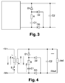
Figure 3 presents another embodiment of a snubber circuit, included secondary side rectifier D3 and output capacitor C2. -
Figure 4 presents another embodiment of a snubber circuit connected to a coupled inductor with secondary side rectifier D3, output capacitor C2 and the load added. - The
figure 5, 6 and7 present different measurements made using circuitry according to the present divulgation. - The
figure 8 presents another embodiment of a snubber circuit - The
figure 9 presents another embodiment of a snubber circuit - In the present document, the word "exemplary" is used herein to mean "serving as an example, instance, or illustration." Any embodiment or implementation of the present subject matter described herein as "exemplary" is not necessarily to be construed as preferred or advantageous over other embodiments.
- An embodiment of the present subject matter is a snubber circuit. This snubber circuit is adapted to limit energy leaking from two terminals of a winding. By winding we mean a circuit comprising a wire or a conductor which constitutes a coil.
- Within the present subject matter the circuitry with bothersome leakage is a converter with two sides, so called primary and secondary side. Each side is galvanically isolated of each other by use of a transformer or a coupled inductor. These components present the unwanted leakage inductances. In general one also could think about using the circuitry object of the present subject matter for a non-isolated type, e.g. a buck or step down converter. But here we don't have this type of leakage but only much lower parasitic inductances caused by e.g. the layout.
-
Figure 2 presents an snubber circuit of the present subject matter. This snubber circuit is adapted to limit energy leaking from a first terminal and a second terminal of a winding 201. The snubber circuit comprises - a first rectifier D1 and a second rectifier D2 and a third rectifier D3 and
- a first capacitor C1 and a second capacitor C2
- In an embodiment the rectifier D3 can be obtain via different type of elements, for example diodes or field effect transistors (FET). The field effect transistor is more complex (additional driver circuitry is needed) but can increase system efficiency a lot. Especially for low output voltages (the diode losses are avoided). If the rectifier is a diode it could be for example silicium fast switching diode or a Schottky diode. The choice between these two types of diode depends on required blocking voltage. In all case the diode needs to be of fast diode type and capable to handle the output current for short periods. The rectifiers D1 or D2 could be a diode for example silicium fast switching diode or a Schottky diode.
- In an embodiment of the present subject matter the first rectifier D1 is a fast switching silicium diode or a Schottky diode and/or
the second rectifier D2 is a fast switching silicium diode or a Schottky diode and/or
the third rectifier D3 is a fast switching silicium diode or a Schottky diode or a field effect transistor. - In an embodiment the first capacitor C1 is a film capacitor or a ceramic capacitor.
- The capacitors, of the present subject matter, need to be a low ESR type and to be capable of handling pulse currents.
- The capacitor C1 likely has a capacity in the nF (nano farad) range. When the leakage inductance (L1) of the choke is known, a first assumption of value of C1 can be to use formula:

- Wherein C1 is the capacity of the first capacitor and I0 is the maximum output current of the winding (202) and dUC the wanted first capacitor (C1) voltage and L1 is the leakage inductance of a coupled inductor of the winding (202). The value of this capacity must be finely tune by performing try and error.
- The
figure 3 presents another embodiment of the present subject matter. In this embodiment the first terminal of the first capacitor C1 is connected to the cathode of the third diode D3 via a resistance R. - In an embodiment the resistance R is below 10 Ohm. The exact value of this resistance depends on what the expected performance of the snubber circuit, more precisely how much damping of remaining oscillation is wanted at the cost of efficiency loss. For example the value of the resistance R could be 1 ohm.
- In an embodiment presented
figure 4 , the winding comprises a coupled inductor, the coupled inductor comprising a first and a second side and a switch configured to applied a voltage across the primary side of the coupled inductor when the switch is turn on, and wherein the snubber circuit is connected to the second side of the coupled inductor. In thefigure 4 the dots closed to the coupled inductor represent the starting point of each winding. It is presupposed that the winding directions are identical. So this is also indication of voltage polarities that establish. - Compared to the snubber of the state of the art, the embodiments of the present subject matter heavily reduce spikes and ringing at the secondary side switch node. Furthermore the circuit efficiency is almost not compromised. Also these snubber circuits add only a minimal additional expenses indeed there is only two diodes plus a capacitor to add. Furthermore to the reduced peak to peak voltage a lower voltage rectifier diode could be used. This further could increase the total circuit efficiency and/or reduce costs.
- In other words by using the circuit of the different embodiments, with primary switch S on, voltage Vin is applied across the primary side of the coupled inductor L. Accordingly (dotted arrows, the dots at the symbol for coupled inductor L define the winding orientation) an inverted voltage on the secondary side establishes. Rectifier diode D3 is blocking in this state and following energy is stored in coupled inductor L. When S is switched off, primary and secondary side voltage polarities reverse (BLACK arrows) and the stored energy is transferred to the secondary side of the converter (D3 now conducts). With next switching-on of S, secondary side leakage current (so the output current) doesn't have a path to go to and following will establish a high positive voltage pike at the cathode of D3. With the given circuitry (C1, R and D1) a path for this current is created. The leakage inductance caused current now flows thru these components charging C1 (dashed arrow), storing the leakage energy. Not considering reverse recovery times, D2 and D3 are blocking in this state. Referring to
figure 1-b , for this operating state the proposed circuitry is quite similar. With next switching-off of S, when the voltages across the windings swap again, the stored energy in C1 is recovered via D2 as part of the output current and mostly not dissipated in a resistive element. You'll note the difference to circuitry according 1b) above, where this energy is burned. Obviously some losses of the small signal diodes D1 and D2 (with high peak current capability) need to be considered. R (drawn dashed) above is not needed mandatory but will damp remaining high frequency oscillations at the cost of some losses. - The
figure 5, 6 and7 present different measurements made using some of the circuits of the present divulgation. The input voltage is 5V, the output voltage is -52V, the output current is 0.6A, and the switching frequency is about 450kHz. - The
figure 5 is a measurement made when no snubber circuit is used. This measurement presents high voltage spikes and heavy ringing. - The
figure 6 is a measurement made using the snubber circuits of thefigure 4 , in this snubber circuits C1=2.2nF and is a type MLCC 100V capacitor and R=1Ω (1ohm). The diode D1 and D2 are BAS16H (silicon switching diode, case SOD-323, 100V, 6ns). In comparison with the measurement offigure 5 , the voltage spikes are heavily reduced and ringing is damped. - The
figure 7 presents the comparison of the efficiency of an inverting boost converter with snubber circuit according tofigure 4 , measurement with the triangles, and an inverting boost converter without snubber circuit, measurement with the circles. Thisfigure 7 highlights that there is no decrease of efficiency with the proposed snubber circuit of figure. - The
figure 8 presents another embodiment of the present subject matter. Within this embodiment the snubber circuit is of the type non-inverting boost converter or isolated flyback. - The
figure 9 presents another embodiment of the present subject matter. Within this embodiment the snubber circuit is of the type forward converter.
wherein an anode of the first rectifier D1 is connected to a cathode of the second rectifier D2
wherein an anode of the third rectifier D3 is connected to anode of the second rectifier D2
wherein a cathode of the third rectifier D3 is connected to the second terminal and to a first terminal of the first capacitor C1
wherein a second terminal of the first capacitor C1 is connected to the anode of the first rectifier D1
wherein a first terminal of the second capacitor C2 is connected to the first terminal of the winding and a second terminal of the second capacitor C2 is connected to the anode of the third rectifier D3.
Claims (8)
- Snubber circuit, adapted to to limit energy leaking from a first terminal and a second terminal of a winding (201), the snubber circuit comprising• a first rectifier (D1) and a second rectifier (D2) and a third rectifier (D3) and• a first capacitor (C1) and a second capacitor (C2)
wherein a cathode of first rectifier (D1) is connected to the first terminal
wherein an anode of the first rectifier (D1) is connected to a cathode of the second rectifier (D2) wherein an anode of the third rectifier (D3) is connected to anode of the second rectifier (D2) wherein a cathode of the third rectifier (D3) is connected to the second terminal and to a first terminal of the first capacitor (C1)
wherein a second terminal of the first capacitor (C1) is connected to the anode of the first rectifier (D1)
wherein a first terminal of the second capacitor (C2) is connected to the first terminal of the winding (201) and a second terminal of the second capacitor (C2) is connected to the anode of the third rectifier (D3). - Snubber circuit according to claim 1 wherein, the first rectifier (D1) and/or the second rectifier (D2) and/or a diode.
- Snubber circuit according to claim 1 wherin the first rectifier (D1) is a fast switching silicium diode or a Schottky diode and/or
the second rectifier (D2) is a fast switching silicium diode or a Schottky diode and/or
the third rectifier (D3) is a fast switching silicium diode or a Schottky diode or a field effect transistor. - Snubber circuit according to claim 1 wherein the first capacitor (C1) is a film capacitor or a ceramic capacitor and wherein the capacity of the first capacitor (C1) is obtained using the formula:

Wherein:C1 is the capacity of the first capacitor andI0 is the maximum output current of the winding (201) anddUC the wanted first capacitor (C1) voltage andL1 is the leakage inductance of a coupled inductor of the winding (201) - Snubber circuit according to any of the previous claims;
wherein the first terminal of the first capacitor (C1) is connected to the cathode of the third diode (D3) via a resistance (R) - Snubber circuit according to claim 4 wherein
a value of the resistance (R) is below 10 ohm, more particularly the value is 1 ohm. - Electronic circuit comprising;
the snubber circuit according to any of the claims 1 to 6 connected to two terminals of the winding (201). - Electronic circuit according to claim 7 wherein the winding (201) comprises a coupled inductor, comprising a first and a second side
the winding also comprises a switch configured to applied a voltage across the primary side of the coupled inductor when the switch is turn on,
and wherein the snubber circuit is connected to the second side of the coupled inductor.
Priority Applications (1)
| Application Number | Priority Date | Filing Date | Title |
|---|---|---|---|
| EP15306998.4A EP3182573A1 (en) | 2015-12-14 | 2015-12-14 | Snubber circuits adapted to limit energy leaking from two terminals of a winding and electronic circuit |
Applications Claiming Priority (1)
| Application Number | Priority Date | Filing Date | Title |
|---|---|---|---|
| EP15306998.4A EP3182573A1 (en) | 2015-12-14 | 2015-12-14 | Snubber circuits adapted to limit energy leaking from two terminals of a winding and electronic circuit |
Publications (1)
| Publication Number | Publication Date |
|---|---|
| EP3182573A1 true EP3182573A1 (en) | 2017-06-21 |
Family
ID=55068929
Family Applications (1)
| Application Number | Title | Priority Date | Filing Date |
|---|---|---|---|
| EP15306998.4A Withdrawn EP3182573A1 (en) | 2015-12-14 | 2015-12-14 | Snubber circuits adapted to limit energy leaking from two terminals of a winding and electronic circuit |
Country Status (1)
| Country | Link |
|---|---|
| EP (1) | EP3182573A1 (en) |
Cited By (1)
| Publication number | Priority date | Publication date | Assignee | Title |
|---|---|---|---|---|
| WO2021018522A1 (en) * | 2019-07-30 | 2021-02-04 | Robert Bosch Gmbh | A voltage clamp circuit |
Citations (4)
| Publication number | Priority date | Publication date | Assignee | Title |
|---|---|---|---|---|
| US5896284A (en) * | 1995-08-11 | 1999-04-20 | Nippon Steel Corporation | Switching power supply apparatus with a return circuit that provides a return energy to a load |
| US20060244428A1 (en) * | 2003-02-11 | 2006-11-02 | Jitaru Ionel D | Active snubber |
| JP2010088209A (en) * | 2008-09-30 | 2010-04-15 | Nichicon Corp | Snubber circuit |
| JP2013027096A (en) * | 2011-07-19 | 2013-02-04 | Murata Mfg Co Ltd | Snubber circuit |
-
2015
- 2015-12-14 EP EP15306998.4A patent/EP3182573A1/en not_active Withdrawn
Patent Citations (4)
| Publication number | Priority date | Publication date | Assignee | Title |
|---|---|---|---|---|
| US5896284A (en) * | 1995-08-11 | 1999-04-20 | Nippon Steel Corporation | Switching power supply apparatus with a return circuit that provides a return energy to a load |
| US20060244428A1 (en) * | 2003-02-11 | 2006-11-02 | Jitaru Ionel D | Active snubber |
| JP2010088209A (en) * | 2008-09-30 | 2010-04-15 | Nichicon Corp | Snubber circuit |
| JP2013027096A (en) * | 2011-07-19 | 2013-02-04 | Murata Mfg Co Ltd | Snubber circuit |
Cited By (1)
| Publication number | Priority date | Publication date | Assignee | Title |
|---|---|---|---|---|
| WO2021018522A1 (en) * | 2019-07-30 | 2021-02-04 | Robert Bosch Gmbh | A voltage clamp circuit |
Similar Documents
| Publication | Publication Date | Title |
|---|---|---|
| US9673722B2 (en) | Quasi-resonant half-bridge converter and control method thereof | |
| US20180342958A1 (en) | Llc resonant converter and electronic device | |
| CN101944851A (en) | The energy of power inverter recovers buffer circuit | |
| US10170973B1 (en) | Synchronous rectifier circuit and switching power supply apparatus | |
| JPH09149640A (en) | Switching power supply and control method thereof | |
| JP4963724B2 (en) | Switching power supply, control circuit for controlling switching power supply, and switching power supply control method | |
| EP2814165B1 (en) | DC Power Supply | |
| CN106105004A (en) | Switching power circuit | |
| JP2019129610A (en) | Waveform shaping circuit, semiconductor device, and switching power supply device | |
| Li et al. | Analysis of a 48V-12V hybrid switched capacitor converter with DC winding current autotransformer | |
| US6487094B1 (en) | High efficiency DC-DC power converter | |
| CN112751487A (en) | DC-DC power converter and method for DC-DC power converter | |
| US9582016B2 (en) | Boost converter with capacitive boost stages | |
| EP3182573A1 (en) | Snubber circuits adapted to limit energy leaking from two terminals of a winding and electronic circuit | |
| US10020746B2 (en) | DC-DC converter with overvoltage protection | |
| US7505289B2 (en) | Flyback DC/DC converter using clamp diode | |
| JP2016082792A (en) | Charger | |
| JP6129244B2 (en) | DC / DC converter | |
| EP3965280A1 (en) | Flyback converter and electronic device | |
| JP2002125370A (en) | Snubber circuit | |
| JP2017055544A (en) | Power factor improvement circuit and power supply device | |
| JP6945429B2 (en) | Insulated switching power supply | |
| JP2021132418A (en) | Switching power supply | |
| KR100729840B1 (en) | Isolated Buck-Boost Converter | |
| JP2015008589A (en) | Switching power-supply device |
Legal Events
| Date | Code | Title | Description |
|---|---|---|---|
| PUAI | Public reference made under article 153(3) epc to a published international application that has entered the european phase |
Free format text: ORIGINAL CODE: 0009012 |
|
| AK | Designated contracting states |
Kind code of ref document: A1 Designated state(s): AL AT BE BG CH CY CZ DE DK EE ES FI FR GB GR HR HU IE IS IT LI LT LU LV MC MK MT NL NO PL PT RO RS SE SI SK SM TR |
|
| AX | Request for extension of the european patent |
Extension state: BA ME |
|
| RAP1 | Party data changed (applicant data changed or rights of an application transferred) |
Owner name: ALCATEL LUCENT |
|
| STAA | Information on the status of an ep patent application or granted ep patent |
Free format text: STATUS: THE APPLICATION IS DEEMED TO BE WITHDRAWN |
|
| 18D | Application deemed to be withdrawn |
Effective date: 20171222 |