EP3182518A1 - Electrical connector - Google Patents
Electrical connector Download PDFInfo
- Publication number
- EP3182518A1 EP3182518A1 EP15200211.9A EP15200211A EP3182518A1 EP 3182518 A1 EP3182518 A1 EP 3182518A1 EP 15200211 A EP15200211 A EP 15200211A EP 3182518 A1 EP3182518 A1 EP 3182518A1
- Authority
- EP
- European Patent Office
- Prior art keywords
- contact
- connector
- contact element
- pin
- plate
- Prior art date
- Legal status (The legal status is an assumption and is not a legal conclusion. Google has not performed a legal analysis and makes no representation as to the accuracy of the status listed.)
- Granted
Links
Images






Classifications
-
- H—ELECTRICITY
- H01—ELECTRIC ELEMENTS
- H01R—ELECTRICALLY-CONDUCTIVE CONNECTIONS; STRUCTURAL ASSOCIATIONS OF A PLURALITY OF MUTUALLY-INSULATED ELECTRICAL CONNECTING ELEMENTS; COUPLING DEVICES; CURRENT COLLECTORS
- H01R12/00—Structural associations of a plurality of mutually-insulated electrical connecting elements, specially adapted for printed circuits, e.g. printed circuit boards [PCB], flat or ribbon cables, or like generally planar structures, e.g. terminal strips, terminal blocks; Coupling devices specially adapted for printed circuits, flat or ribbon cables, or like generally planar structures; Terminals specially adapted for contact with, or insertion into, printed circuits, flat or ribbon cables, or like generally planar structures
- H01R12/50—Fixed connections
- H01R12/51—Fixed connections for rigid printed circuits or like structures
- H01R12/515—Terminal blocks providing connections to wires or cables
-
- H—ELECTRICITY
- H01—ELECTRIC ELEMENTS
- H01R—ELECTRICALLY-CONDUCTIVE CONNECTIONS; STRUCTURAL ASSOCIATIONS OF A PLURALITY OF MUTUALLY-INSULATED ELECTRICAL CONNECTING ELEMENTS; COUPLING DEVICES; CURRENT COLLECTORS
- H01R12/00—Structural associations of a plurality of mutually-insulated electrical connecting elements, specially adapted for printed circuits, e.g. printed circuit boards [PCB], flat or ribbon cables, or like generally planar structures, e.g. terminal strips, terminal blocks; Coupling devices specially adapted for printed circuits, flat or ribbon cables, or like generally planar structures; Terminals specially adapted for contact with, or insertion into, printed circuits, flat or ribbon cables, or like generally planar structures
- H01R12/50—Fixed connections
- H01R12/51—Fixed connections for rigid printed circuits or like structures
- H01R12/55—Fixed connections for rigid printed circuits or like structures characterised by the terminals
- H01R12/58—Fixed connections for rigid printed circuits or like structures characterised by the terminals terminals for insertion into holes
- H01R12/585—Terminals having a press fit or a compliant portion and a shank passing through a hole in the printed circuit board
-
- H—ELECTRICITY
- H01—ELECTRIC ELEMENTS
- H01R—ELECTRICALLY-CONDUCTIVE CONNECTIONS; STRUCTURAL ASSOCIATIONS OF A PLURALITY OF MUTUALLY-INSULATED ELECTRICAL CONNECTING ELEMENTS; COUPLING DEVICES; CURRENT COLLECTORS
- H01R4/00—Electrically-conductive connections between two or more conductive members in direct contact, i.e. touching one another; Means for effecting or maintaining such contact; Electrically-conductive connections having two or more spaced connecting locations for conductors and using contact members penetrating insulation
- H01R4/24—Connections using contact members penetrating or cutting insulation or cable strands
- H01R4/2416—Connections using contact members penetrating or cutting insulation or cable strands the contact members having insulation-cutting edges, e.g. of tuning fork type
- H01R4/242—Connections using contact members penetrating or cutting insulation or cable strands the contact members having insulation-cutting edges, e.g. of tuning fork type the contact members being plates having a single slot
-
- H—ELECTRICITY
- H01—ELECTRIC ELEMENTS
- H01R—ELECTRICALLY-CONDUCTIVE CONNECTIONS; STRUCTURAL ASSOCIATIONS OF A PLURALITY OF MUTUALLY-INSULATED ELECTRICAL CONNECTING ELEMENTS; COUPLING DEVICES; CURRENT COLLECTORS
- H01R12/00—Structural associations of a plurality of mutually-insulated electrical connecting elements, specially adapted for printed circuits, e.g. printed circuit boards [PCB], flat or ribbon cables, or like generally planar structures, e.g. terminal strips, terminal blocks; Coupling devices specially adapted for printed circuits, flat or ribbon cables, or like generally planar structures; Terminals specially adapted for contact with, or insertion into, printed circuits, flat or ribbon cables, or like generally planar structures
- H01R12/70—Coupling devices
- H01R12/7005—Guiding, mounting, polarizing or locking means; Extractors
- H01R12/7011—Locking or fixing a connector to a PCB
- H01R12/7052—Locking or fixing a connector to a PCB characterised by the locating members
Definitions
- the invention refers to an electrical connector according to claim 1.
- the object of the invention is to provide an improved electrical connector for connecting an electrical conductor with an electrical contact.
- the object of the invention is attained by the electrical connector according to claim 1.
- An advantage of the provided electrical connector is to disclose a simple constructed electrical connector that allows an easy and robust electrical connection between an electrical conductor and an electrical contact.
- This advantage is attained by providing an electrical connector with a first contact element with an isolation displacement contact and a second contact element with a contact pin.
- the isolation displacement contact allows a simple contacting of the electrical conductor that comprises an isolating cover and an electrical conducting core. Furthermore the contact pin can easily be pushed in a contact opening of the printed circuit board.
- the isolation displacement contact is connected by a flexible connecting element with the contact pin. Therefore a flexible connection between the first and second contact element is provided.
- the connecting element comprises a plate and the first contact element is connected with the plate. This embodiment provides a simple and strong connection between the first and the second contact element.
- the flexible connecting element comprises a bended section.
- the bended section is preferably arranged in a plane parallel to a longitudinal axis of the contact pin. Therefore the first and the second contact element can be arranged with a small distance and a high flexible connecting element, because the connecting element has enough space.
- the contact pin is connected by the connection element with a plate, wherein the contact pin, the connecting element and the plate are made in one piece and made of the same material, and wherein the first contact element is fixed to the plate.
- the first contact element is made of a different material than the first contact element, preferably the plate. Therefore the material for the first and the second contact element can be selected for the specific function of the first and the second contact element. This improves the property of the connector.
- the connector comprises a guiding pin.
- the guiding pin is preferably provided for being inserted in a centering hole for example of a printed circuit board for aligning the connector in a predetermined position.
- the guiding pin allows a precise alignment of the connector according to a longitudinal axis of the conductor.
- the guiding pin and the contact pin are arranged at opposite sides of the connector.
- the guiding pin is made in one piece and made of the same material as the first contact element. Therefore a simple embodiment of the connector is provided.
- the plate comprises a recess and the guiding pin is guided through the recess. This embodiment improves the alignment of the second contact element.
- the first contact element comprises a web rib that is arranged on the connecting element.
- the web rib stabilizes the connection between the first and the second contact element.
- the first contact element comprises two isolation displacement contacts, wherein the isolation displacement contacts are arranged in one plane at opposite sides of the first contact element. This arrangement improves the contact force between the first contact element and the electrical conductor.
- the two isolation displacement contacts are connected by two side walls, wherein the two side walls are made of one piece with a bottom wall, wherein the bottom wall is connected to the plate, wherein the side walls preferably comprise stiffening elements adjacent to the bottom plate.
- the isolation displacement contacts are embodied as side parts of the side walls.
- the side parts of the two opposite side walls define a receiving area for the electrical conductor.
- the receiving area decreases in an insertion direction, but at a lower end the receiving area increases to a broader section. This arrangement increases the flexibility of the side walls.
- the contact pin comprise a broader section with two abutting planes that define a maximum insertion depth of the contact pin in a contact hole of a printed circuit board.
- Fig. 1 shows in a perspective view an embodiment of an electrical connector 1 for connecting an electrical conductor with an electrical contact for example with an electrical contact of a printed circuit board.
- a coordinate system with a Z-axis, a Y-axis and a X-axis is depicted, wherein the Z-, the Y- and the X-axis are perpendicular to each other.
- the electrical connector 1 comprises a first contact element 2 that is embodied for connecting the electrical conductor.
- the electrical connector 1 comprises a second contact element 3 that is embodied to connect the electrical contact.
- the first contact element 2 is embodied as an isolation displacement contact 4, named idc contact in the following.
- the shown embodiment comprises two idc contacts 4,5.
- the two idc contacts 4, 5 are arranged at opposite sides of the first contact element 2 referring to a longitudinal Y-axis.
- the two idc contacts 4, 5 are embodied by two walls 6, 7 that have a U-shape and that are arranged at opposite sides with regard to a middle plane that corresponds to a Z-Y-plane.
- Each side wall comprises a middle section 10 and a first and a second side part 8,9 at opposite endings of the wall 6,7.
- the two side parts 8,9 of each wall 6, 7 are arranged in a given angle for example 90° with respect to a Z-Y-plane of the middle section.
- the middle sections are arranged parallel to the Z-Y-plane with a given distance along the X-axis.
- Opposite side parts 8, 9 of the first and the second side wall 6,7 define a first and a second receiving area 11, 12 for an electrical conductor.
- the two receiving areas 11, 12 are arranged with a given distance along the Y-axis at opposite ends of the first contact element 2.
- the two first opposite side parts 8 and the two second opposite side parts 9 of the two side walls 6, 7 are arranged at a given distance along the X-axis providing the first and a second receiving area 11, 12.
- the first and the second wall 6, 7 are connected to a bottom wall 13.
- the bottom wall 13 is arranged in a Y-X-plane.
- the bottom wall 13 comprises a guiding pin 14 that extends from the bottom wall 13 in an opposite Z-direction than the walls 6, 7. Depending on the used embodiment the guiding pin 14 can be omitted.
- the first contact element 2 is arranged on a plate 15.
- the plate 15 is arranged in a Y-X-plane and comprises in the shown embodiment a recess 16, wherein the guiding pin 14 is guided through the recess 16.
- the plate 15 is connected by a connecting element 17 with the second contact element 3.
- the second contact element 3 is embodied as a contact pin 18.
- the plate 15, the connecting element 17 and the contact pin 18 are made in one piece and made of the same material.
- the connecting element 17 comprises a bended section 52 and connects flexibly the contact pin 18 with the plate 15 and therefore with the first contact element 2.
- the connecting element 17 comprises in the shown embodiment a U-shape that is arranged in a Z-Y-plane perpendicular to the Y-X-plane of the plate 15.
- the contact pin 18 is in the shown embodiment also arranged with a longitudinal axis along a Z-axis and perpendicular to the Y-X-plane of the plate 15.
- the connecting element 17 may also have a different shape that allows a flexible connection between the contact pin and the plate 15.
- the bended section 52 i.e. the U-shape may be arranged in a Y-X-plane or in any other orientation.
- the bended section 52 may also have a S-shape.
- the contact pin 18 comprises a formable section 19 that is provided to provide a press fit connection to a contact hole for example of a printed circuit board. Furthermore, the contact pin comprises in the shown embodiment a broader section 20 with two abutting planes 21, 22. The two abutting planes 21,22 define a maximum insertion depth of the contact pin 18 in a contact hole.
- the first contact element 2 comprises stiffening sections 23 at a transition section between the first wall 6 and the bottom wall 13 and between the second wall 7 and a bottom wall 13.
- the stiffening section 23 may be embodied as press-in recesses that increase the mechanical stability of the first and the second wall 6, 7.
- the first side parts 8 and the second side parts 9 are embodied as straps that are only connected with the first or the second wall 6, 7. The side parts 8, 9 are not connected with the bottom wall 13.
- Fig. 2 shows a top view of the electrical connector of Fig. 1 .
- the first contact element 2 is fixed with the bottom wall 13 to the plate 15.
- the bottom wall 13 is fixed by welding points 50 with the plate 15.
- the first contact element 2 is made of a different material than the plate 15 and the second contact element 3.
- the first contact element 2 is made of a material that provides properties that are of advantage for an idc contact.
- the second contact element 3 is made of a material that is of advantage for providing a contact pin and a connecting element.
- the material of the first contact element 2 may have a higher stiffness than the material of the second contact element 3.
- the first contact element 2 comprises depending on the used embodiment a web rib 44 that is part of the bottom wall 13 and that is arranged on a section of the plate 15 and/or on a section of the connecting element 17.
- the web rib 44 protrudes from the bottom wall 13 in a Y-X-plane and extends a predetermined distance along the Y-axis.
- the web rib 44 increases the stability of the connection between the first and the second contact element 2,3.
- Fig. 3 shows a side view of the electrical connector 1 of the Figs. 1 and 2 .
- the side parts 8, 9 of the walls 6, 7 are not connected with the bottom wall 13 but only connected with the middle sections 10.
- the U-form shape of the connecting element 17 is clearly shown. This means that the receiving areas 11,12 increase at a lower section compared to a middle section. At an upper section the receiving areas decrease in the insertion direction and comprise for example a V-shape.
- Fig. 4 shows a packaging condition with several electrical connectors 1 that are arranged as a ribbon 51.
- the electrical connectors 1 are connected via the plates 15.
- This ribbon of electrical connectors 1 can be used for providing a placement machine with a ribbon of electrical connectors 1.
- Fig. 5 shows in a schematic view a part of a printed circuit board 24.
- the printed circuit board (pcb) 24 comprises several centering holes 25 and several contact holes 26.
- any other kind of substrate with a centering hole 25 and/or a contact hole 26 may be used for mounting the electrical connectors.
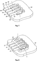
- Fig. 6 shows the printed circuit board 24 of Fig. 5 with several mounted electrical connectors 1.
- the contact pins 18 are pushed in the contact holes 26 and the guiding pins 14 are pushed in the centering holes 25.
- This arrangement allows a precise alignment of the electrical connectors 1 with respect to a predetermined axis. Therefore the electrical connectors 1 can be arranged in a predetermined arrangement for example in a parallel arrangement.
- the electrical connectors 1 of Fig. 6 are separated.
- Fig. 7 shows the arrangement of Fig. 6 , wherein electrical conductors 27 are mounted on the first contact elements 2.
- the electrical conductors 27 comprise an insulation cover 28 and an electrical conducting core 29.
- the insulation cover 28 is displaced and a direct mechanical contact is provided between the core 29 of the electrical conductors and the side parts 8, 9 of the walls 6, 7.
- the electrical conductors 27 may be embodied as line wire.
- Fig. 8 shows the arrangement of Fig. 7 , wherein a protective cover 30 is arranged in the area of the first contact elements 2 of the electrical connectors 1.
- the cover 30 may be made of insulating material for example glue material or polyethylene.
- the cover 30 protects the idc contacts 4, 5 and increases a fixing force between the electrical conductors 27 to the electrical connectors 1.
- the contact pins 18 are electrically connected to electrical contacts of the printed circuit board 24. Furthermore the formable section 19 of the contact pins 18 are connected by a press-fit connection to the contact holes 26.
- the cover 30 is omitted as shown in Fig. 7 .
- Fig. 9 shows a further embodiment of an electrical connector 1 with a first and a second contact element 2, 3 that has the same design and the same structure and material as the electrical connector of Fig. 1 .
- the first contact element 2 does not comprise a guiding pin but comprises higher middle sections 10 of the first and the second wall 6, 7 that project higher along the Z-axis compared to the connector 1 of Fig.1 .
- the second contact element 3 comprises a plate 15 and a connecting element and a contact pin 18 that are arranged in a Y-X-plane.
- Fig. 10 shows a top view of the electrical connector 1 of Fig. 9 .
- Fig. 11 shows a side view of the electrical connector 1 of Fig. 9 and 10 .
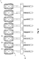
- Fig. 12 shows an arrangement of several electrical connectors 1 that are provided as a ribbon 51 for feeding a placement machine.
- the electrical connectors 1 are connected with a first and a second connecting section 31, 32.
- the first connecting section 31 is arranged between the contact pins 18 and a second connecting section 32 is arranged between the plates 15.
- the first and the second connecting sections 31,32 are divided before the electrical connectors 1 are mounted on the pcb by the placing machine.
- Fig. 13 shows a further embodiment of a printed circuit board 24, wherein in this embodiment contact holes 26 and connector holes 33 are arranged.
- the connector holes 33 are connected in a middle section.
- the printed circuit board 24 may comprise only one connector hole 33 or several separated connector holes 33.
- Fig. 14 shows a crimping tool 34 in a perspective view.
- the crimping tool 34 comprises several crimping elements 38.
- Each crimping element 38 is provided for one electrical conductor.
- Each crimping element 38 comprises a first, a second and a third plane 35,36,37 that are arranged in a Y-axis and separated by recesses 39, 40. Additionally the crimping elements 38 are separated along the X-axis by further recesses 41.
- the crimping tool of Fig. 14 may comprise only one crimping element 38 or two or more crimping elements 38.
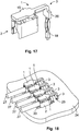
- Fig. 15 shows an arrangement with the printed circuit board 24 of Fig. 13 with an inserted crimping tool 34 and several electrical conductors 27 that are aligned along the Y-axis and laid on the crimping elements 38 of the crimping tool 34.
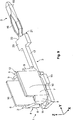
- Fig. 16 shows a bottom view of the electrical connector 1 of Figs. 9 to 11 .
- the electrical connector 1 is prepared for mounting on the printed circuit board 24 by bending the contact pin 18 with a predetermined angle to the plane of the plate 15 as shown in Fig. 17 .
- the contact pin 18 is arranged perpendicular to the plane of the plate 15.
- This prepared electrical connector 1 is then pushed on the electrical conductors and the crimping tool 34 as shown in
- Fig. 18 The contact pins 18 are introduced in the contact holes 26 and the first contact elements 2 of the electrical connectors 1 are pushed on the crimping tool 34.
- the first and second side parts 8, 9 of the walls 6, 7 are arranged in the first and the second recess 39, 40.
- the middle section 10 of the walls 6, 7 of the first contact element 2 are arranged within the further recesses 41 of the crimping tool 34.
- a cover 30 may be disposed on the printed circuit board 24 covering a section of the electrical conductors 27 adjacent to the electrical connectors 1. This process step is shown in Fig. 19 .
- the cover 30 may be a protective glue, polyethylene or a potting material dispensed on the electrical conductors 27 adjacent to the electrical connectors 1.
- the cover 30 fixes the conductors with the pcb 24 and/or with the electrical connectors 1.
- a further cover 42 may be disposed on a bottom side 43 of the printed circuit board 24 filling up and/or covering the connector holes 33 as shown in Fig. 20 .
- a top side or on a bottom side 43 of the printed circuit board 24 further contacts are arranged that are electrically connected with the contact pins 18.
Landscapes
- Coupling Device And Connection With Printed Circuit (AREA)
Abstract
Description
- The invention refers to an electrical connector according to
claim 1. - In the state of the art different electrical connectors are known that connect an electrical conductor with a printed circuit board.
- The object of the invention is to provide an improved electrical connector for connecting an electrical conductor with an electrical contact.
- The object of the invention is attained by the electrical connector according to
claim 1. - Further embodiments of the electrical connector are disclosed in the dependent claims.
- An advantage of the provided electrical connector is to disclose a simple constructed electrical connector that allows an easy and robust electrical connection between an electrical conductor and an electrical contact. This advantage is attained by providing an electrical connector with a first contact element with an isolation displacement contact and a second contact element with a contact pin. The isolation displacement contact allows a simple contacting of the electrical conductor that comprises an isolating cover and an electrical conducting core. Furthermore the contact pin can easily be pushed in a contact opening of the printed circuit board. The isolation displacement contact is connected by a flexible connecting element with the contact pin. Therefore a flexible connection between the first and second contact element is provided.
- In a further embodiment, the connecting element comprises a plate and the first contact element is connected with the plate. This embodiment provides a simple and strong connection between the first and the second contact element.
- In a further embodiment, the flexible connecting element comprises a bended section. The bended section is preferably arranged in a plane parallel to a longitudinal axis of the contact pin. Therefore the first and the second contact element can be arranged with a small distance and a high flexible connecting element, because the connecting element has enough space.
- In a further embodiment, the contact pin is connected by the connection element with a plate, wherein the contact pin, the connecting element and the plate are made in one piece and made of the same material, and wherein the first contact element is fixed to the plate. This embodiment provides a robust electrical connector that can be easily fabricated.
- In a further embodiment, the first contact element is made of a different material than the first contact element, preferably the plate. Therefore the material for the first and the second contact element can be selected for the specific function of the first and the second contact element. This improves the property of the connector.
- In a further embodiment, the connector comprises a guiding pin. The guiding pin is preferably provided for being inserted in a centering hole for example of a printed circuit board for aligning the connector in a predetermined position. The guiding pin allows a precise alignment of the connector according to a longitudinal axis of the conductor.
- In a further embodiment the guiding pin and the contact pin are arranged at opposite sides of the connector.
- In a further embodiment the guiding pin is made in one piece and made of the same material as the first contact element. Therefore a simple embodiment of the connector is provided.
- In a further embodiment the plate comprises a recess and the guiding pin is guided through the recess. This embodiment improves the alignment of the second contact element.
- In a further embodiment the first contact element comprises a web rib that is arranged on the connecting element. The web rib stabilizes the connection between the first and the second contact element.
- In a further embodiment the first contact element comprises two isolation displacement contacts, wherein the isolation displacement contacts are arranged in one plane at opposite sides of the first contact element. This arrangement improves the contact force between the first contact element and the electrical conductor.
- In a further embodiment the two isolation displacement contacts are connected by two side walls, wherein the two side walls are made of one piece with a bottom wall, wherein the bottom wall is connected to the plate, wherein the side walls preferably comprise stiffening elements adjacent to the bottom plate. This arrangement provides a simple and robust design for the first contact element.
- In a further embodiment the isolation displacement contacts are embodied as side parts of the side walls. The side parts of the two opposite side walls define a receiving area for the electrical conductor. The receiving area decreases in an insertion direction, but at a lower end the receiving area increases to a broader section. This arrangement increases the flexibility of the side walls.
- In a further embodiment the contact pin comprise a broader section with two abutting planes that define a maximum insertion depth of the contact pin in a contact hole of a printed circuit board.
- In a further embodiment several connector are connected to a ribbon for supplying a place machine with.
- So that the manner in which the above recited features of the electrical connector can be understood in detail, a more particular description of the electrical connector, briefly summarized above, may be had by reference to embodiments, some of which are illustrated in the appended drawings. It is to be noted, however, that the appended drawings illustrate only typical embodiments of this invention and are therefore not to be considered limiting of its scope, for the invention may admit to other equally effective embodiments.
-
Fig. 1 shows a perspective view of a first embodiment of the electrical connector. -
Fig. 2 shows a top view of the electrical connector, -
Fig. 3 shows a side view of the electrical connector, -
Fig. 4 shows a packaging condition of electrical connectors, -
Fig. 5 shows a schematic partial view of a printed circuit board with centering holes and contact holes, -
Fig. 6 shows a printed circuit board with mounted electrical connectors, -
Fig. 7 shows a printed circuit board with mounted electrical connectors and connected electrical conductors, -
Fig. 8 shows the arrangement ofFig. 7 with a protective cover, -
Fig. 9 shows a perspective view of a further electrical connector, -
Fig. 10 shows a top view of the further electrical connector, -
Fig. 11 shows a side view of the further electrical connector, -
Fig. 12 shows a packaging condition of further electrical connectors, -
Fig. 13 shows a schematic partial view of a further printed circuit board, -
Fig. 14 shows a schematic view of a crimping tool, -
Fig. 15 shows a schematic view of the printed circuit board with the crimping tool and electrical conductors, -
Fig. 16 shows a further perspective view of the further electrical connector, -
Fig. 17 shows the further electrical connector ofFig. 16 with a bended second contact element, -
Fig. 18 shows the arrangement ofFig. 15 with mounted electrical connectors ofFig. 17 , -
Fig. 19 shows the arrangement ofFig. 18 with a protective cover, and -
Fig. 20 shows the arrangement ofFig. 19 from a bottom view. - In the following, reference is made to embodiments of the invention. However, it should be understood that the invention is not limited to specific described embodiments. Instead, any combination of the following features and elements, whether related to different embodiments or not, is contemplated to implement in practice the invention. Furthermore, in various embodiments the invention provides numerous advantages over the prior art. However, although embodiments of the invention may achieve advantages over other possible solutions and/or over the prior art, whether or not a particular advantage is achieved by a given embodiment is not limiting of the invention. Thus, the following aspects, features, embodiments and advantages are merely illustrative and are not considered elements or limitations of the appended claims except where explicitly recited in a claim.
-
Fig. 1 shows in a perspective view an embodiment of anelectrical connector 1 for connecting an electrical conductor with an electrical contact for example with an electrical contact of a printed circuit board. A coordinate system with a Z-axis, a Y-axis and a X-axis is depicted, wherein the Z-, the Y- and the X-axis are perpendicular to each other. Theelectrical connector 1 comprises afirst contact element 2 that is embodied for connecting the electrical conductor. Furthermore, theelectrical connector 1 comprises asecond contact element 3 that is embodied to connect the electrical contact. Thefirst contact element 2 is embodied as anisolation displacement contact 4, named idc contact in the following. The shown embodiment comprises twoidc contacts idc contacts first contact element 2 referring to a longitudinal Y-axis. The twoidc contacts walls middle section 10 and a first and asecond side part wall side parts wall side parts second side wall second receiving area areas first contact element 2. The two firstopposite side parts 8 and the two secondopposite side parts 9 of the twoside walls second receiving area second wall bottom wall 13. Thebottom wall 13 is arranged in a Y-X-plane. Furthermore thebottom wall 13 comprises a guidingpin 14 that extends from thebottom wall 13 in an opposite Z-direction than thewalls pin 14 can be omitted. - The
first contact element 2 is arranged on aplate 15. Theplate 15 is arranged in a Y-X-plane and comprises in the shown embodiment arecess 16, wherein the guidingpin 14 is guided through therecess 16. Theplate 15 is connected by a connectingelement 17 with thesecond contact element 3. Thesecond contact element 3 is embodied as acontact pin 18. Theplate 15, the connectingelement 17 and thecontact pin 18 are made in one piece and made of the same material. The connectingelement 17 comprises abended section 52 and connects flexibly thecontact pin 18 with theplate 15 and therefore with thefirst contact element 2. The connectingelement 17 comprises in the shown embodiment a U-shape that is arranged in a Z-Y-plane perpendicular to the Y-X-plane of theplate 15. Thecontact pin 18 is in the shown embodiment also arranged with a longitudinal axis along a Z-axis and perpendicular to the Y-X-plane of theplate 15. Depending on the used embodiment, the connectingelement 17 may also have a different shape that allows a flexible connection between the contact pin and theplate 15. For example thebended section 52, i.e. the U-shape may be arranged in a Y-X-plane or in any other orientation. Thebended section 52 may also have a S-shape. - In the shown embodiment, the
contact pin 18 comprises aformable section 19 that is provided to provide a press fit connection to a contact hole for example of a printed circuit board. Furthermore, the contact pin comprises in the shown embodiment abroader section 20 with two abuttingplanes planes contact pin 18 in a contact hole. - In the shown embodiment the
first contact element 2 comprises stiffeningsections 23 at a transition section between thefirst wall 6 and thebottom wall 13 and between thesecond wall 7 and abottom wall 13. Thestiffening section 23 may be embodied as press-in recesses that increase the mechanical stability of the first and thesecond wall first side parts 8 and thesecond side parts 9 are embodied as straps that are only connected with the first or thesecond wall side parts bottom wall 13. -
Fig. 2 shows a top view of the electrical connector ofFig. 1 . Thefirst contact element 2 is fixed with thebottom wall 13 to theplate 15. For example thebottom wall 13 is fixed by weldingpoints 50 with theplate 15. Depending on the used embodiment, thefirst contact element 2 is made of a different material than theplate 15 and thesecond contact element 3. Thefirst contact element 2 is made of a material that provides properties that are of advantage for an idc contact. Thesecond contact element 3 is made of a material that is of advantage for providing a contact pin and a connecting element. The material of thefirst contact element 2 may have a higher stiffness than the material of thesecond contact element 3. Thefirst contact element 2 comprises depending on the used embodiment aweb rib 44 that is part of thebottom wall 13 and that is arranged on a section of theplate 15 and/or on a section of the connectingelement 17. Theweb rib 44 protrudes from thebottom wall 13 in a Y-X-plane and extends a predetermined distance along the Y-axis. Theweb rib 44 increases the stability of the connection between the first and thesecond contact element -
Fig. 3 shows a side view of theelectrical connector 1 of theFigs. 1 and 2 . In this view, it is clearly shown that theside parts walls bottom wall 13 but only connected with themiddle sections 10. Furthermore the U-form shape of the connectingelement 17 is clearly shown. This means that the receivingareas -
Fig. 4 shows a packaging condition with severalelectrical connectors 1 that are arranged as aribbon 51. Theelectrical connectors 1 are connected via theplates 15. This ribbon ofelectrical connectors 1 can be used for providing a placement machine with a ribbon ofelectrical connectors 1. -
Fig. 5 shows in a schematic view a part of a printedcircuit board 24. The printed circuit board (pcb) 24 comprises several centeringholes 25 and several contact holes 26. Depending on the used embodiment, instead of apcb 24 also any other kind of substrate with a centeringhole 25 and/or acontact hole 26 may be used for mounting the electrical connectors. -
Fig. 6 shows the printedcircuit board 24 ofFig. 5 with several mountedelectrical connectors 1. The contact pins 18 are pushed in the contact holes 26 and the guiding pins 14 are pushed in the centering holes 25. This arrangement allows a precise alignment of theelectrical connectors 1 with respect to a predetermined axis. Therefore theelectrical connectors 1 can be arranged in a predetermined arrangement for example in a parallel arrangement. Theelectrical connectors 1 ofFig. 6 are separated. -
Fig. 7 shows the arrangement ofFig. 6 , whereinelectrical conductors 27 are mounted on thefirst contact elements 2. Theelectrical conductors 27 comprise aninsulation cover 28 and anelectrical conducting core 29. During the mounting of theelectrical conductor 27 in theidc contacts first contact element 2 theinsulation cover 28 is displaced and a direct mechanical contact is provided between the core 29 of the electrical conductors and theside parts walls electrical conductors 27 may be embodied as line wire. -
Fig. 8 shows the arrangement ofFig. 7 , wherein aprotective cover 30 is arranged in the area of thefirst contact elements 2 of theelectrical connectors 1. Thecover 30 may be made of insulating material for example glue material or polyethylene. Thecover 30 protects theidc contacts electrical conductors 27 to theelectrical connectors 1. The contact pins 18 are electrically connected to electrical contacts of the printedcircuit board 24. Furthermore theformable section 19 of the contact pins 18 are connected by a press-fit connection to the contact holes 26. Depending on the used embodiment, thecover 30 is omitted as shown inFig. 7 . -
Fig. 9 shows a further embodiment of anelectrical connector 1 with a first and asecond contact element Fig. 1 . In the shown embodiment, thefirst contact element 2 does not comprise a guiding pin but comprises highermiddle sections 10 of the first and thesecond wall connector 1 ofFig.1 . Additionally at the shown embodiment thesecond contact element 3 comprises aplate 15 and a connecting element and acontact pin 18 that are arranged in a Y-X-plane. -
Fig. 10 shows a top view of theelectrical connector 1 ofFig. 9 . -
Fig. 11 shows a side view of theelectrical connector 1 ofFig. 9 and10 . -
Fig. 12 shows an arrangement of severalelectrical connectors 1 that are provided as aribbon 51 for feeding a placement machine. In this embodiment theelectrical connectors 1 are connected with a first and a second connectingsection section 31 is arranged between the contact pins 18 and a second connectingsection 32 is arranged between theplates 15. The first and the second connectingsections electrical connectors 1 are mounted on the pcb by the placing machine. -
Fig. 13 shows a further embodiment of a printedcircuit board 24, wherein in this embodiment contact holes 26 and connector holes 33 are arranged. The connector holes 33 are connected in a middle section. Furthermore, depending on the used embodiment, the printedcircuit board 24 may comprise only oneconnector hole 33 or several separated connector holes 33. -
Fig. 14 shows a crimpingtool 34 in a perspective view. The crimpingtool 34 comprises several crimpingelements 38. Each crimpingelement 38 is provided for one electrical conductor. Each crimpingelement 38 comprises a first, a second and athird plane recesses elements 38 are separated along the X-axis by further recesses 41. Depending on the used embodiment the crimping tool ofFig. 14 may comprise only one crimpingelement 38 or two or more crimpingelements 38. -
Fig. 15 shows an arrangement with the printedcircuit board 24 ofFig. 13 with an inserted crimpingtool 34 and severalelectrical conductors 27 that are aligned along the Y-axis and laid on the crimpingelements 38 of the crimpingtool 34. -
Fig. 16 shows a bottom view of theelectrical connector 1 ofFigs. 9 to 11 . Theelectrical connector 1 is prepared for mounting on the printedcircuit board 24 by bending thecontact pin 18 with a predetermined angle to the plane of theplate 15 as shown inFig. 17 . In the shown embodiment thecontact pin 18 is arranged perpendicular to the plane of theplate 15. - This prepared
electrical connector 1 is then pushed on the electrical conductors and the crimpingtool 34 as shown in -
Fig. 18 . The contact pins 18 are introduced in the contact holes 26 and thefirst contact elements 2 of theelectrical connectors 1 are pushed on the crimpingtool 34. The first andsecond side parts walls second recess middle section 10 of thewalls first contact element 2 are arranged within the further recesses 41 of the crimpingtool 34. - Depending on the used embodiment, a
cover 30 may be disposed on the printedcircuit board 24 covering a section of theelectrical conductors 27 adjacent to theelectrical connectors 1. This process step is shown inFig. 19 . Thecover 30 may be a protective glue, polyethylene or a potting material dispensed on theelectrical conductors 27 adjacent to theelectrical connectors 1. Thecover 30 fixes the conductors with thepcb 24 and/or with theelectrical connectors 1. - Depending on the used embodiment after removing the crimping
tool 34 also afurther cover 42 may be disposed on abottom side 43 of the printedcircuit board 24 filling up and/or covering the connector holes 33 as shown inFig. 20 . Depending on the used embodiment on a top side or on abottom side 43 of the printedcircuit board 24 further contacts are arranged that are electrically connected with the contact pins 18. -
- 1
- electrical connector
- 2
- first contact element
- 3
- second contact element
- 4
- first isolation displacement contact
- 5
- second isolation displacement contact
- 6
- first wall
- 7
- second wall
- 8
- first side part
- 9
- second side part
- 10
- middle section
- 11
- first receiving area
- 12
- second receiving area
- 13
- bottom plate
- 14
- guiding pin
- 15
- plate
- 16
- recess
- 17
- connecting element
- 18
- contact pin
- 19
- formable section
- 20
- broader section
- 21
- first abutting plane
- 22
- second abutting plane
- 23
- stiffening section
- 24
- printed circuit board
- 25
- centering hole
- 26
- contact hole
- 27
- electrical conductor
- 28
- insulation cover
- 29
- conducting core
- 30
- cover
- 31
- first connecting section
- 32
- second connecting section
- 33
- connector hole
- 34
- crimping tool
- 35
- first plane
- 36
- second plane
- 37
- third plane
- 38
- crimping element
- 39
- first recess
- 40
- second recess
- 41
- further recess
- 42
- further cover
- 43
- bottom side
- 44
- web rib
- 50
- welding point
- 51
- ribbon
- 52
- bending section
Claims (16)
- Electrical connector (1) for connecting an electrical conductor (27) with an electrical contact, with a first contact element (2) for connecting the electrical conductor (27), with a second contact element (3) for connecting the electrical contact, wherein the first contact element (2) comprises an isolation displacement contact (4, 5) for connecting the electrical conductor, wherein the second contact element (3) comprises a contact pin (18) for connecting the electrical contact, wherein the second contact element (3) comprises a connecting element (17), wherein the first contact element (3) is connected with the connecting element, wherein the connecting element comprises a flexible section.
- Connector of claim 1, wherein the second contact element (3) comprises a plate (15), wherein the plate (15) is connected by the connecting element (17) with the contact pin (18), and wherein the first contact element (2) is connected with the plate (15).
- Connector of claim 2, wherein the flexible section is a bended section (52), wherein the bended section (52) is preferably arranged in a plane perpendicular to the plane of the plate (15), and wherein the bended section is preferably arranged in a plane parallel to a longitudinal axis of the contact pin (18).
- Connector of one of the preceding claims, wherein the contact pin (18) is connected by the connecting element (17) with a plate (15), wherein the contact pin (18), the connecting element (17) and the plate (15) are made in one piece and made of the same material, and wherein the first contact element (2) is fixed to the plate (15).
- Connector of one of the precedent claims, wherein the first contact element (2) is made of a different material compared to the second contact element (3).
- Connector of one of the preceding claims, wherein the connector comprises a guiding pin (14), wherein the guiding pin (14) projects in a similar direction as the contact pin from the connector, wherein the guiding pin is provided for being inserted in a centering hole for aligning the connector in a predetermined position.
- Connector of claim 6, wherein the guiding pin (14) and the contact pin (18) are arranged at opposite sides of the connector (1).
- Connector of claim 6 or 7, wherein the guiding pin (14) is made in one piece and made of the same material as the first contact element (2).
- Connector of the claims 2 and 8, wherein the plate (15) comprises a recess (16), and wherein the guiding pin (14) is part of the first contact element (2) and guided through the recess (16).
- Connector of one of the preceding claims 2 to 9, wherein the first contact element (2) comprises a bottom wall (13), wherein the bottom wall (13) is arranged on the plate (15), wherein the bottom wall (13) comprises a web rib (44) that projects from the bottom wall (13), wherein the web rib (44) is arranged on the connecting element (17) stabilizing the connection between the first and the second contact element (2, 3).
- Connector of one of the preceding claims, wherein the first contact element (2) comprises two isolation displacement contacts (4, 5), wherein the isolation displacement contacts are arranged at opposite sides of the first contact element (2).
- Connector of claim 11, wherein the two isolation displacement contacts (4, 5) are defined by two walls (6, 7), wherein the two walls (6, 7) are made in one piece with a bottom wall (13), wherein the bottom wall (13) is connected to the plate (15), wherein the walls (6, 7) preferably comprise stiffening elements (23) adjacent to the bottom wall (13).
- Connector of claim 12, wherein the isolation displacement contacts are embodied as side parts (8, 9) of the walls (6, 7), wherein the receiving area (11, 12) of the isolation displacement contacts (4, 5) comprises a broader section at a lower end of the receiving area (11, 12).
- Connector of one of the preceding claims, wherein the contact pin (18) comprises a broader section (20) with an abutting plane (21) that defines a maximum insertion depth of the contact pin (18) in a contact hole.
- Connector of one of the preceding claims, wherein the connector (1) is arranged on a printed circuit board (24), and wherein the contact pin (18) is arranged in a contact hole (26) of the printed circuit board (24).
- Connector of one of the preceding claims, wherein several connectors (1) are connected to a ribbon (51) for supplying a placement machine with connectors (1).
Priority Applications (1)
| Application Number | Priority Date | Filing Date | Title |
|---|---|---|---|
| EP15200211.9A EP3182518B1 (en) | 2015-12-15 | 2015-12-15 | Electrical connector |
Applications Claiming Priority (1)
| Application Number | Priority Date | Filing Date | Title |
|---|---|---|---|
| EP15200211.9A EP3182518B1 (en) | 2015-12-15 | 2015-12-15 | Electrical connector |
Publications (2)
| Publication Number | Publication Date |
|---|---|
| EP3182518A1 true EP3182518A1 (en) | 2017-06-21 |
| EP3182518B1 EP3182518B1 (en) | 2022-08-03 |
Family
ID=54850041
Family Applications (1)
| Application Number | Title | Priority Date | Filing Date |
|---|---|---|---|
| EP15200211.9A Active EP3182518B1 (en) | 2015-12-15 | 2015-12-15 | Electrical connector |
Country Status (1)
| Country | Link |
|---|---|
| EP (1) | EP3182518B1 (en) |
Citations (4)
| Publication number | Priority date | Publication date | Assignee | Title |
|---|---|---|---|---|
| EP0243998A1 (en) * | 1986-04-03 | 1987-11-04 | E.I. Du Pont De Nemours And Company | Contact strip |
| DE20307168U1 (en) * | 2003-05-08 | 2003-07-03 | WECO Wester, Ebbinghaus GmbH & Co. KG, 63452 Hanau | Electrical terminal block has blade and anvil combination to receive the cable end |
| US20070010139A1 (en) * | 2005-07-08 | 2007-01-11 | J.S.T. Corporation | Press-fit pin |
| WO2010146525A1 (en) * | 2009-06-15 | 2010-12-23 | Claudio Manca | Low cost clamp for connection of electric wires or cables on printed circuits |
Family Cites Families (1)
| Publication number | Priority date | Publication date | Assignee | Title |
|---|---|---|---|---|
| EP2665128B1 (en) * | 2012-05-14 | 2017-12-13 | TE Connectivity Germany GmbH | IDC contact element for an electrical plug |
-
2015
- 2015-12-15 EP EP15200211.9A patent/EP3182518B1/en active Active
Patent Citations (4)
| Publication number | Priority date | Publication date | Assignee | Title |
|---|---|---|---|---|
| EP0243998A1 (en) * | 1986-04-03 | 1987-11-04 | E.I. Du Pont De Nemours And Company | Contact strip |
| DE20307168U1 (en) * | 2003-05-08 | 2003-07-03 | WECO Wester, Ebbinghaus GmbH & Co. KG, 63452 Hanau | Electrical terminal block has blade and anvil combination to receive the cable end |
| US20070010139A1 (en) * | 2005-07-08 | 2007-01-11 | J.S.T. Corporation | Press-fit pin |
| WO2010146525A1 (en) * | 2009-06-15 | 2010-12-23 | Claudio Manca | Low cost clamp for connection of electric wires or cables on printed circuits |
Also Published As
| Publication number | Publication date |
|---|---|
| EP3182518B1 (en) | 2022-08-03 |
Similar Documents
| Publication | Publication Date | Title |
|---|---|---|
| EP2822101B1 (en) | Connector terminal and connector housing used for the same | |
| US10525906B2 (en) | Branch structure and wire harness | |
| US10457229B2 (en) | Branch structure and wire harness | |
| CN104103925B (en) | Electrical contact and the electric coupler component for including it | |
| US10797414B2 (en) | Cable connector for coaxial cable on thick printed-circuit board | |
| KR20120022624A (en) | Electrical connector and circuit board assembly | |
| US10468792B2 (en) | Terminal block | |
| CN105048134A (en) | Interlocking poke home contact | |
| US10665970B2 (en) | Plug-in contact | |
| CN101369693A (en) | electrical connector | |
| US9414491B2 (en) | Jumper module mounting circuit board and circuit board assembly | |
| CN103515891B (en) | Electric connection box | |
| WO2015060085A1 (en) | Printed circuit board, electronic device provided with printed circuit board, and manufacturing method for printed circuit board | |
| US20170054225A1 (en) | Joint connector and wire harness | |
| CN104931736A (en) | Attachment structure of current sensor and electric conductive member | |
| EP3876353B1 (en) | Terminal block and terminal block set | |
| KR100735351B1 (en) | Wiring board with connector and manufacturing method thereof | |
| US9437946B2 (en) | Printed circuit board assembly having improved terminals | |
| US20110232960A1 (en) | Component-equipped-holder mounting structure | |
| EP3182518A1 (en) | Electrical connector | |
| KR101488892B1 (en) | Connector assembly for board-to-board | |
| KR102165739B1 (en) | Hold down of connector and connector including the same | |
| KR102148179B1 (en) | Connector assembly | |
| US6951475B2 (en) | Cable strain relief device | |
| US8313341B1 (en) | Guide element for a connector device |
Legal Events
| Date | Code | Title | Description |
|---|---|---|---|
| PUAI | Public reference made under article 153(3) epc to a published international application that has entered the european phase |
Free format text: ORIGINAL CODE: 0009012 |
|
| STAA | Information on the status of an ep patent application or granted ep patent |
Free format text: STATUS: THE APPLICATION HAS BEEN PUBLISHED |
|
| AK | Designated contracting states |
Kind code of ref document: A1 Designated state(s): AL AT BE BG CH CY CZ DE DK EE ES FI FR GB GR HR HU IE IS IT LI LT LU LV MC MK MT NL NO PL PT RO RS SE SI SK SM TR |
|
| AX | Request for extension of the european patent |
Extension state: BA ME |
|
| STAA | Information on the status of an ep patent application or granted ep patent |
Free format text: STATUS: REQUEST FOR EXAMINATION WAS MADE |
|
| 17P | Request for examination filed |
Effective date: 20171219 |
|
| RBV | Designated contracting states (corrected) |
Designated state(s): AL AT BE BG CH CY CZ DE DK EE ES FI FR GB GR HR HU IE IS IT LI LT LU LV MC MK MT NL NO PL PT RO RS SE SI SK SM TR |
|
| STAA | Information on the status of an ep patent application or granted ep patent |
Free format text: STATUS: EXAMINATION IS IN PROGRESS |
|
| 17Q | First examination report despatched |
Effective date: 20180517 |
|
| GRAP | Despatch of communication of intention to grant a patent |
Free format text: ORIGINAL CODE: EPIDOSNIGR1 |
|
| STAA | Information on the status of an ep patent application or granted ep patent |
Free format text: STATUS: GRANT OF PATENT IS INTENDED |
|
| RIC1 | Information provided on ipc code assigned before grant |
Ipc: H01R 12/58 20110101ALI20200910BHEP Ipc: H01R 12/70 20110101ALN20200910BHEP Ipc: H01R 4/242 20180101AFI20200910BHEP Ipc: H01R 12/51 20110101ALI20200910BHEP |
|
| RIC1 | Information provided on ipc code assigned before grant |
Ipc: H01R 12/70 20110101ALN20200911BHEP Ipc: H01R 12/58 20110101ALI20200911BHEP Ipc: H01R 4/242 20180101AFI20200911BHEP Ipc: H01R 12/51 20110101ALI20200911BHEP |
|
| INTG | Intention to grant announced |
Effective date: 20200930 |
|
| GRAJ | Information related to disapproval of communication of intention to grant by the applicant or resumption of examination proceedings by the epo deleted |
Free format text: ORIGINAL CODE: EPIDOSDIGR1 |
|
| STAA | Information on the status of an ep patent application or granted ep patent |
Free format text: STATUS: EXAMINATION IS IN PROGRESS |
|
| INTC | Intention to grant announced (deleted) | ||
| REG | Reference to a national code |
Ref country code: DE Ref legal event code: R079 Ref document number: 602015080120 Country of ref document: DE Free format text: PREVIOUS MAIN CLASS: H01R0004240000 Ipc: H01R0004242000 |
|
| GRAP | Despatch of communication of intention to grant a patent |
Free format text: ORIGINAL CODE: EPIDOSNIGR1 |
|
| STAA | Information on the status of an ep patent application or granted ep patent |
Free format text: STATUS: GRANT OF PATENT IS INTENDED |
|
| RIC1 | Information provided on ipc code assigned before grant |
Ipc: H01R 12/70 20110101ALN20220120BHEP Ipc: H01R 12/58 20110101ALI20220120BHEP Ipc: H01R 12/51 20110101ALI20220120BHEP Ipc: H01R 4/242 20180101AFI20220120BHEP |
|
| RIC1 | Information provided on ipc code assigned before grant |
Ipc: H01R 12/70 20110101ALN20220127BHEP Ipc: H01R 12/58 20110101ALI20220127BHEP Ipc: H01R 12/51 20110101ALI20220127BHEP Ipc: H01R 4/242 20180101AFI20220127BHEP |
|
| INTG | Intention to grant announced |
Effective date: 20220215 |
|
| GRAS | Grant fee paid |
Free format text: ORIGINAL CODE: EPIDOSNIGR3 |
|
| GRAA | (expected) grant |
Free format text: ORIGINAL CODE: 0009210 |
|
| STAA | Information on the status of an ep patent application or granted ep patent |
Free format text: STATUS: THE PATENT HAS BEEN GRANTED |
|
| AK | Designated contracting states |
Kind code of ref document: B1 Designated state(s): AL AT BE BG CH CY CZ DE DK EE ES FI FR GB GR HR HU IE IS IT LI LT LU LV MC MK MT NL NO PL PT RO RS SE SI SK SM TR |
|
| REG | Reference to a national code |
Ref country code: AT Ref legal event code: REF Ref document number: 1509501 Country of ref document: AT Kind code of ref document: T Effective date: 20220815 Ref country code: CH Ref legal event code: EP |
|
| REG | Reference to a national code |
Ref country code: DE Ref legal event code: R096 Ref document number: 602015080120 Country of ref document: DE |
|
| REG | Reference to a national code |
Ref country code: IE Ref legal event code: FG4D |
|
| REG | Reference to a national code |
Ref country code: LT Ref legal event code: MG9D |
|
| REG | Reference to a national code |
Ref country code: NL Ref legal event code: MP Effective date: 20220803 |
|
| PG25 | Lapsed in a contracting state [announced via postgrant information from national office to epo] |
Ref country code: SE Free format text: LAPSE BECAUSE OF FAILURE TO SUBMIT A TRANSLATION OF THE DESCRIPTION OR TO PAY THE FEE WITHIN THE PRESCRIBED TIME-LIMIT Effective date: 20220803 Ref country code: RS Free format text: LAPSE BECAUSE OF FAILURE TO SUBMIT A TRANSLATION OF THE DESCRIPTION OR TO PAY THE FEE WITHIN THE PRESCRIBED TIME-LIMIT Effective date: 20220803 Ref country code: PT Free format text: LAPSE BECAUSE OF FAILURE TO SUBMIT A TRANSLATION OF THE DESCRIPTION OR TO PAY THE FEE WITHIN THE PRESCRIBED TIME-LIMIT Effective date: 20221205 Ref country code: NO Free format text: LAPSE BECAUSE OF FAILURE TO SUBMIT A TRANSLATION OF THE DESCRIPTION OR TO PAY THE FEE WITHIN THE PRESCRIBED TIME-LIMIT Effective date: 20221103 Ref country code: NL Free format text: LAPSE BECAUSE OF FAILURE TO SUBMIT A TRANSLATION OF THE DESCRIPTION OR TO PAY THE FEE WITHIN THE PRESCRIBED TIME-LIMIT Effective date: 20220803 Ref country code: LV Free format text: LAPSE BECAUSE OF FAILURE TO SUBMIT A TRANSLATION OF THE DESCRIPTION OR TO PAY THE FEE WITHIN THE PRESCRIBED TIME-LIMIT Effective date: 20220803 Ref country code: LT Free format text: LAPSE BECAUSE OF FAILURE TO SUBMIT A TRANSLATION OF THE DESCRIPTION OR TO PAY THE FEE WITHIN THE PRESCRIBED TIME-LIMIT Effective date: 20220803 Ref country code: FI Free format text: LAPSE BECAUSE OF FAILURE TO SUBMIT A TRANSLATION OF THE DESCRIPTION OR TO PAY THE FEE WITHIN THE PRESCRIBED TIME-LIMIT Effective date: 20220803 Ref country code: ES Free format text: LAPSE BECAUSE OF FAILURE TO SUBMIT A TRANSLATION OF THE DESCRIPTION OR TO PAY THE FEE WITHIN THE PRESCRIBED TIME-LIMIT Effective date: 20220803 |
|
| REG | Reference to a national code |
Ref country code: AT Ref legal event code: MK05 Ref document number: 1509501 Country of ref document: AT Kind code of ref document: T Effective date: 20220803 |
|
| PG25 | Lapsed in a contracting state [announced via postgrant information from national office to epo] |
Ref country code: PL Free format text: LAPSE BECAUSE OF FAILURE TO SUBMIT A TRANSLATION OF THE DESCRIPTION OR TO PAY THE FEE WITHIN THE PRESCRIBED TIME-LIMIT Effective date: 20220803 Ref country code: IS Free format text: LAPSE BECAUSE OF FAILURE TO SUBMIT A TRANSLATION OF THE DESCRIPTION OR TO PAY THE FEE WITHIN THE PRESCRIBED TIME-LIMIT Effective date: 20221203 Ref country code: HR Free format text: LAPSE BECAUSE OF FAILURE TO SUBMIT A TRANSLATION OF THE DESCRIPTION OR TO PAY THE FEE WITHIN THE PRESCRIBED TIME-LIMIT Effective date: 20220803 Ref country code: GR Free format text: LAPSE BECAUSE OF FAILURE TO SUBMIT A TRANSLATION OF THE DESCRIPTION OR TO PAY THE FEE WITHIN THE PRESCRIBED TIME-LIMIT Effective date: 20221104 |
|
| PG25 | Lapsed in a contracting state [announced via postgrant information from national office to epo] |
Ref country code: SM Free format text: LAPSE BECAUSE OF FAILURE TO SUBMIT A TRANSLATION OF THE DESCRIPTION OR TO PAY THE FEE WITHIN THE PRESCRIBED TIME-LIMIT Effective date: 20220803 Ref country code: RO Free format text: LAPSE BECAUSE OF FAILURE TO SUBMIT A TRANSLATION OF THE DESCRIPTION OR TO PAY THE FEE WITHIN THE PRESCRIBED TIME-LIMIT Effective date: 20220803 Ref country code: DK Free format text: LAPSE BECAUSE OF FAILURE TO SUBMIT A TRANSLATION OF THE DESCRIPTION OR TO PAY THE FEE WITHIN THE PRESCRIBED TIME-LIMIT Effective date: 20220803 Ref country code: CZ Free format text: LAPSE BECAUSE OF FAILURE TO SUBMIT A TRANSLATION OF THE DESCRIPTION OR TO PAY THE FEE WITHIN THE PRESCRIBED TIME-LIMIT Effective date: 20220803 Ref country code: AT Free format text: LAPSE BECAUSE OF FAILURE TO SUBMIT A TRANSLATION OF THE DESCRIPTION OR TO PAY THE FEE WITHIN THE PRESCRIBED TIME-LIMIT Effective date: 20220803 |
|
| REG | Reference to a national code |
Ref country code: DE Ref legal event code: R097 Ref document number: 602015080120 Country of ref document: DE |
|
| PG25 | Lapsed in a contracting state [announced via postgrant information from national office to epo] |
Ref country code: SK Free format text: LAPSE BECAUSE OF FAILURE TO SUBMIT A TRANSLATION OF THE DESCRIPTION OR TO PAY THE FEE WITHIN THE PRESCRIBED TIME-LIMIT Effective date: 20220803 Ref country code: EE Free format text: LAPSE BECAUSE OF FAILURE TO SUBMIT A TRANSLATION OF THE DESCRIPTION OR TO PAY THE FEE WITHIN THE PRESCRIBED TIME-LIMIT Effective date: 20220803 |
|
| PLBE | No opposition filed within time limit |
Free format text: ORIGINAL CODE: 0009261 |
|
| STAA | Information on the status of an ep patent application or granted ep patent |
Free format text: STATUS: NO OPPOSITION FILED WITHIN TIME LIMIT |
|
| PG25 | Lapsed in a contracting state [announced via postgrant information from national office to epo] |
Ref country code: AL Free format text: LAPSE BECAUSE OF FAILURE TO SUBMIT A TRANSLATION OF THE DESCRIPTION OR TO PAY THE FEE WITHIN THE PRESCRIBED TIME-LIMIT Effective date: 20220803 |
|
| 26N | No opposition filed |
Effective date: 20230504 |
|
| REG | Reference to a national code |
Ref country code: CH Ref legal event code: PL |
|
| GBPC | Gb: european patent ceased through non-payment of renewal fee |
Effective date: 20221215 |
|
| REG | Reference to a national code |
Ref country code: BE Ref legal event code: MM Effective date: 20221231 |
|
| PG25 | Lapsed in a contracting state [announced via postgrant information from national office to epo] |
Ref country code: SI Free format text: LAPSE BECAUSE OF FAILURE TO SUBMIT A TRANSLATION OF THE DESCRIPTION OR TO PAY THE FEE WITHIN THE PRESCRIBED TIME-LIMIT Effective date: 20220803 Ref country code: LU Free format text: LAPSE BECAUSE OF NON-PAYMENT OF DUE FEES Effective date: 20221215 |
|
| PG25 | Lapsed in a contracting state [announced via postgrant information from national office to epo] |
Ref country code: LI Free format text: LAPSE BECAUSE OF NON-PAYMENT OF DUE FEES Effective date: 20221231 Ref country code: IE Free format text: LAPSE BECAUSE OF NON-PAYMENT OF DUE FEES Effective date: 20221215 Ref country code: GB Free format text: LAPSE BECAUSE OF NON-PAYMENT OF DUE FEES Effective date: 20221215 Ref country code: CH Free format text: LAPSE BECAUSE OF NON-PAYMENT OF DUE FEES Effective date: 20221231 |
|
| PG25 | Lapsed in a contracting state [announced via postgrant information from national office to epo] |
Ref country code: FR Free format text: LAPSE BECAUSE OF NON-PAYMENT OF DUE FEES Effective date: 20221231 Ref country code: BE Free format text: LAPSE BECAUSE OF NON-PAYMENT OF DUE FEES Effective date: 20221231 |
|
| PG25 | Lapsed in a contracting state [announced via postgrant information from national office to epo] |
Ref country code: HU Free format text: LAPSE BECAUSE OF FAILURE TO SUBMIT A TRANSLATION OF THE DESCRIPTION OR TO PAY THE FEE WITHIN THE PRESCRIBED TIME-LIMIT; INVALID AB INITIO Effective date: 20151215 |
|
| PG25 | Lapsed in a contracting state [announced via postgrant information from national office to epo] |
Ref country code: CY Free format text: LAPSE BECAUSE OF FAILURE TO SUBMIT A TRANSLATION OF THE DESCRIPTION OR TO PAY THE FEE WITHIN THE PRESCRIBED TIME-LIMIT Effective date: 20220803 |
|
| PG25 | Lapsed in a contracting state [announced via postgrant information from national office to epo] |
Ref country code: MK Free format text: LAPSE BECAUSE OF FAILURE TO SUBMIT A TRANSLATION OF THE DESCRIPTION OR TO PAY THE FEE WITHIN THE PRESCRIBED TIME-LIMIT Effective date: 20220803 Ref country code: IT Free format text: LAPSE BECAUSE OF FAILURE TO SUBMIT A TRANSLATION OF THE DESCRIPTION OR TO PAY THE FEE WITHIN THE PRESCRIBED TIME-LIMIT Effective date: 20220803 |
|
| PG25 | Lapsed in a contracting state [announced via postgrant information from national office to epo] |
Ref country code: MC Free format text: LAPSE BECAUSE OF FAILURE TO SUBMIT A TRANSLATION OF THE DESCRIPTION OR TO PAY THE FEE WITHIN THE PRESCRIBED TIME-LIMIT Effective date: 20220803 |
|
| PG25 | Lapsed in a contracting state [announced via postgrant information from national office to epo] |
Ref country code: MC Free format text: LAPSE BECAUSE OF FAILURE TO SUBMIT A TRANSLATION OF THE DESCRIPTION OR TO PAY THE FEE WITHIN THE PRESCRIBED TIME-LIMIT Effective date: 20220803 |
|
| PG25 | Lapsed in a contracting state [announced via postgrant information from national office to epo] |
Ref country code: BG Free format text: LAPSE BECAUSE OF FAILURE TO SUBMIT A TRANSLATION OF THE DESCRIPTION OR TO PAY THE FEE WITHIN THE PRESCRIBED TIME-LIMIT Effective date: 20220803 |
|
| PG25 | Lapsed in a contracting state [announced via postgrant information from national office to epo] |
Ref country code: MT Free format text: LAPSE BECAUSE OF FAILURE TO SUBMIT A TRANSLATION OF THE DESCRIPTION OR TO PAY THE FEE WITHIN THE PRESCRIBED TIME-LIMIT Effective date: 20220803 |
|
| PG25 | Lapsed in a contracting state [announced via postgrant information from national office to epo] |
Ref country code: TR Free format text: LAPSE BECAUSE OF FAILURE TO SUBMIT A TRANSLATION OF THE DESCRIPTION OR TO PAY THE FEE WITHIN THE PRESCRIBED TIME-LIMIT Effective date: 20220803 |
|
| PGFP | Annual fee paid to national office [announced via postgrant information from national office to epo] |
Ref country code: DE Payment date: 20250930 Year of fee payment: 11 |