EP3182511A1 - Système antennaire de type réseau - Google Patents
Système antennaire de type réseau Download PDFInfo
- Publication number
- EP3182511A1 EP3182511A1 EP16204890.4A EP16204890A EP3182511A1 EP 3182511 A1 EP3182511 A1 EP 3182511A1 EP 16204890 A EP16204890 A EP 16204890A EP 3182511 A1 EP3182511 A1 EP 3182511A1
- Authority
- EP
- European Patent Office
- Prior art keywords
- elements
- primary
- antenna system
- ports
- port
- Prior art date
- Legal status (The legal status is an assumption and is not a legal conclusion. Google has not performed a legal analysis and makes no representation as to the accuracy of the status listed.)
- Granted
Links
Images



Classifications
-
- H—ELECTRICITY
- H01—ELECTRIC ELEMENTS
- H01Q—ANTENNAS, i.e. RADIO AERIALS
- H01Q5/00—Arrangements for simultaneous operation of antennas on two or more different wavebands, e.g. dual-band or multi-band arrangements
- H01Q5/30—Arrangements for providing operation on different wavebands
- H01Q5/378—Combination of fed elements with parasitic elements
- H01Q5/385—Two or more parasitic elements
-
- H—ELECTRICITY
- H01—ELECTRIC ELEMENTS
- H01Q—ANTENNAS, i.e. RADIO AERIALS
- H01Q21/00—Antenna arrays or systems
- H01Q21/06—Arrays of individually energised antenna units similarly polarised and spaced apart
- H01Q21/061—Two dimensional planar arrays
- H01Q21/065—Patch antenna array
-
- H—ELECTRICITY
- H01—ELECTRIC ELEMENTS
- H01Q—ANTENNAS, i.e. RADIO AERIALS
- H01Q21/00—Antenna arrays or systems
- H01Q21/29—Combinations of different interacting antenna units for giving a desired directional characteristic
- H01Q21/293—Combinations of different interacting antenna units for giving a desired directional characteristic one unit or more being an array of identical aerial elements
- H01Q21/296—Multiplicative arrays
-
- H—ELECTRICITY
- H01—ELECTRIC ELEMENTS
- H01Q—ANTENNAS, i.e. RADIO AERIALS
- H01Q25/00—Antennas or antenna systems providing at least two radiating patterns
- H01Q25/04—Multimode antennas
-
- H—ELECTRICITY
- H01—ELECTRIC ELEMENTS
- H01Q—ANTENNAS, i.e. RADIO AERIALS
- H01Q5/00—Arrangements for simultaneous operation of antennas on two or more different wavebands, e.g. dual-band or multi-band arrangements
- H01Q5/30—Arrangements for providing operation on different wavebands
- H01Q5/307—Individual or coupled radiating elements, each element being fed in an unspecified way
- H01Q5/314—Individual or coupled radiating elements, each element being fed in an unspecified way using frequency dependent circuits or components, e.g. trap circuits or capacitors
- H01Q5/328—Individual or coupled radiating elements, each element being fed in an unspecified way using frequency dependent circuits or components, e.g. trap circuits or capacitors between a radiating element and ground
Definitions
- the invention relates to the field of network-type antenna systems comprising a plurality of excited antenna elements.
- Network-type antennal systems are known in which all the elements are powered. Such a system is complex and expensive because it requires a complex distribution circuit.
- Aerial systems of the lacunary or rarefied type are also known in which one or more elements have been removed from an array of elements.
- the removal of some elements leads to performance degradation and uncertainties in the setting of the excitation of the various elements to achieve desired performance.
- An object of the invention is to provide a network-type antenna system comprising a power supply circuit which is not very complex and therefore inexpensive.
- Another object of the invention is to provide an antenna whose performance can be easily configured.
- Yet another object of the invention is to be less bulky than a conventional type of network antenna, the size greatly depending on the power supply circuit.
- the system is configurable in that the contribution to the radiation pattern of the primary elements is achieved through the optimization of the power supply circuit and the contribution of the secondary elements is achieved through the optimization of complex impedance loads. Similarly, it is possible to configure an operating mode to optimize the adaptation of the system at the same time as the radiation pattern.
- the optimization uses the knowledge of the coupling matrix of the array of radiating elements expressed in each of the ports of the radiating elements.
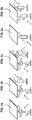
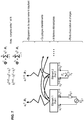
- FIGS. 1a, 1b, 1c, 2a, 2b illustrate basic elements of an antennal system according to the invention.
- the Figures 1a, 1b, 1c illustrate a primary element 1, 1 ', 1 ", comprising at least one access port P (here one or two port (s) access.) At least one access port is excited by a circuit 3 of food ( Figures 1a, 1b, 1c ). In the case of a single access port ( figure 1a ) the latter is excited by the supply circuit 3. In the case of two ports where only one port is excited by the power supply circuit 3 ( figure 1b ) the other is connected to a load 4 of complex impedance jXi. The two P ports of the primary element can also be excited each by the power circuit 3 ( figure 1c ).
- a primary element is thus excited by a power supply circuit 3 shown conceptually in the figures by a generator Eg; a resistance Rg in series. All the primary elements are excited by a supply circuit, in the same way or in a differentiated manner via a weighting in amplitude and phase of the signal.
- FIGS. 2a and 2b illustrate a secondary element 2 ', 2 "comprising at least one access port P (here one or two port (s) of access) Each access port is connected to a complex impedance load 4 jXi.
- Each secondary element is connected to a complex impedance load 4 connected between a ground line and the secondary element 2 (however, depending on the case, the complex loads are not necessarily connected to a common ground line, see below. in the description).
- Each load 4 of complex impedance makes it possible to optimize the phase of the field re-emitted by the secondary element.
- each load 4 is adjustable so that it can be modified as needed.
- the feed circuit 3 and the loads 4 make it possible to configure the radiation patterns which result from the contribution of the primary and secondary elements.
- the charges 4 are reactive to avoid dissipation.
- each element has one or more access ports corresponding to different operating modes (polarization / frequency).
- the primary or secondary element comprises two access ports then they are orthogonal that is to say they are differentiated in polarization and / or frequency.
- the access port corresponds to one or other of the orthogonal modes.
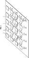
- the figure 3 illustrates an antenna system according to a first embodiment of the invention wherein the primary and secondary elements comprise a single access port. Regarding the primary elements they are all excited by a power circuit.
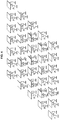
- the figure 4 illustrates an antenna system according to a second embodiment in which the primary and secondary elements both comprise access ports.
- the antennal system according to this first embodiment consists of primary elements of the Figure 1b or 1c and secondary elements of the figure 2b .
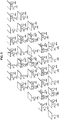
- the figure 5 illustrates an antennal system according to a third embodiment of the invention wherein the primary elements both comprise access ports and the secondary elements comprise one or two access ports.
- the antennal system according to this third embodiment consists of primary elements of the Figure 1b or 1c and secondary elements of the Figure 2a or 2b
- the figure 6 illustrates an antenna system according to a fourth embodiment of the invention wherein the primary elements and the secondary elements all comprise one or two access ports.
- the antennal system according to this fourth embodiment consists of primary elements of the Figure 1a, or 1b or 1c and secondary elements of the Figure 2a or 2b .
- the primary elements are powered and the secondary elements are used to contribute to obtaining the desired performance for the antennal system.
- the supply circuit 3 and the loads 4 are configured so that the level of coupling between each primary element 1 and at least one secondary element 2 is greater than or equal to -23 dB typically.
- the coupling level has a direct influence on the excitation amplitude of the secondary elements, so it must be sufficient for the contribution of the secondary elements to be significant.
- the primary elements 1 are chosen from the following group: patches, dipoles, resonant structure, horns.
- the antenna system of the invention comprises primary and secondary elements, preferably identical, arranged in a periodic grid which is rectangular or triangular.
- the fact of feeding some elements and not others, makes it possible to obtain a better yield related to the surface of the network compared to a gap network for example.
- the primary elements excited by the power supply circuit and all the elements (primary or secondary) that are not excited are in linear polarization (H, V).
- the primary elements excited by the supply circuit and all the elements (primary or secondary) which are not excited are in circular polarization (RHCP, LHCP).
- the primary elements excited by the supply circuit are in circular polarization (RHCP, LHCP) and all the elements (primary or secondary) which are not excited are in polarization linear.
- the antennal system nevertheless operates in circular polarization thanks to the management of the charges connected to the elements in linear polarization.
- the antenna system comprises M radiating elements and N ports, a supply circuit which comprises a first auxiliary supply circuit which performs the excitations E g C and a second auxiliary supply circuit which performs the excitations E g D .
- This number of auxiliary supply circuits is not limiting. So, on the figure 2 some primary elements include two Port 1, Port 2 power ports.
- each of these elements is associated with a surrounding radiation pattern, noted ⁇ n . It will be noted that here the concept of the enclosed diagram is defined for each element radiating at its respective position in the network, or in the sense of an infinite periodic formalism.
- Such an antennal system makes it possible to realize the orthogonality of the diagrams ⁇ C and ⁇ D , these diagrams being the contribution of the environment diagrams weighted by the incident powers.
- a primary element can be powered on one port and connected only to one load on the other so that its behavior is both that of a primary element and that of a secondary element. This also applies in the case of multiple ports.
Landscapes
- Variable-Direction Aerials And Aerial Arrays (AREA)
Abstract
Description
- L'invention concerne le domaine des systèmes antennaires du type réseau comprenant plusieurs éléments d'antennes excités.
- On connait des systèmes antennaires du type réseau dans lesquels tous les éléments sont alimentés. Or un tel système est complexe et coûteux car il nécessite un circuit de répartition complexe.
- On connait également des systèmes antennaires du type lacunaires ou raréfiés dans lesquels on a retiré d'un réseau d'éléments un ou plusieurs éléments. Or la suppression de certains éléments conduit à une dégradation de performance et à des incertitudes quant au réglage de l'excitation des différents éléments pour obtenir des performances souhaitées.
- Un but de l'invention est de proposer un système antennaire de type réseau comprenant un circuit d'alimentation qui est peu complexe et donc peu coûteux.
- Un autre but de l'invention est de proposer une antenne dont les performances peuvent être facilement configurées.
- Encore un autre but de l'invention est d'être moins encombrant qu'une antenne réseau de type classique, l'encombrement dépendant fortement du circuit d'alimentation.
- A cet effet, l'invention propose un système antennaire comprenant un réseau d'éléments d'antennes comprenant :
- une pluralité d'éléments primaires comprenant au moins un port d'accès (P);
- une pluralité d'éléments secondaires comprenant au moins un port d'accès (P) ;
- une pluralité de circuits d'alimentation configurés pour exciter au moins un port d'un élément primaire ;
- une pluralité de charges réactives, idéalement, ou a minima peu dissipatives connectées à
- o un des ports d'un élément primaire si tous les ports dudit élément primaire ne sont pas excités ;
- o un port d'un élément secondaire
- o un des ports d'un élément primaire si tous les ports dudit élément primaire ne sont pas excités ;
- L'invention est avantageusement complétée par les caractéristiques suivantes, prises seules ou en une quelconque de leur combinaison techniquement possible :
- les éléments primaires et secondaires comportent tous deux ports d'accès ;
- les éléments primaires comportent deux ports d'accès et les éléments secondaires comportent un ou deux ports d'accès ;
- les éléments primaires et secondaires comportent un ou deux ports d'accès ;
- le réseau d'éléments d'antennes et configuré pour que le niveau de couplage entre chaque élément primaire et au moins un élément secondaire soit supérieur ou égal à un niveau de -23dB ;
- chaque port d'accès est associé à un mode de fonctionnement, dans le cas de plusieurs ports d'accès, les modes de fonctionnement sont orthogonaux entre eux ;
- les éléments primaires sont choisis dans le groupe suivant : patchs, dipôles, structure résonantes, cornets ;
- le réseau d'éléments d'antennes est disposé selon une grille présentant une maille dont le pas est compris entre 0,2 λ, et 3 λ, λ étant longueur d'onde associée à une fréquence de fonctionnement du système antennaire.
- Les avantages de l'invention sont multiples.
- En utilisant le couplage entre des éléments alimentés et non alimentés par le circuit d'alimentation on peut configurer de manière précise le diagramme de rayonnement du système antennaire tout en ayant un circuit d'alimentation peu complexe (compte tenu que tous les éléments ne sont pas alimentés directement). En revanche, tous les éléments sont excités ; certains directement via le circuit d'alimentation (éléments primaires), les autres par couplage (éléments secondaires).
- Le système est configurable en ce que la contribution au diagramme de rayonnement des éléments primaires s'effectue grâce à l'optimisation du circuit d'alimentation et la contribution des éléments secondaires s'effectue grâce à l'optimisation des charges d'impédances complexes. De même, il est possible de configurer un mode de fonctionnement permettant d'optimiser l'adaptation du système en même temps que le diagramme de rayonnement.
- Il est possible d'optimiser l'adaptation du système en même temps que le diagramme de rayonnement.
- Il est possible de générer des diagrammes orthogonaux en polarisation et/ou en fréquence grâce à l'utilisation de ports séparés en polarisation et/ou en fréquence sur tout ou partie des éléments rayonnants.
- Dans tous les cas, l'optimisation utilise la connaissance de la matrice de couplage du réseau d'éléments rayonnants exprimée en chacun des ports des éléments rayonnants.
- D'autres caractéristiques, buts et avantages de l'invention ressortiront de la description qui suit, qui est purement illustrative et non limitative, et qui doit être lue en regard des dessins annexés sur lesquels :
- les
figures 1a, 1b, 1c, 2a, 2b illustrent des éléments de base d'un système antennaire selon l'invention ; - la
figure 3 illustre une vue d'ensemble d'un système antennaire selon un premier mode de réalisation de l'invention ; - la
figure 4 illustre une vue d'ensemble d'un système antennaire selon un second mode de réalisation de l'invention ; - la
figure 5 illustre une vue d'ensemble d'un système antennaire selon un troisième mode de réalisation de l'invention ; - la
figure 6 illustre une vue d'ensemble d'un système antennaire selon un quatrième mode de réalisation de l'invention ; - la
figure 7 illustre le principe du rayonnement du système antennaire selon l'invention. - Sur l'ensemble des figures les éléments similaires portent des références identiques.
- Les
figures 1a, 1b, 1c, 2a, 2b illustrent des éléments de base d'un système antennaire selon l'invention. - Les
figures 1a, 1b, 1c illustrent un élément primaire 1, 1', 1", comprenant au moins un port P d'accès (ici un ou deux port(s) d'accès). Au moins un port d'accès est excité par un circuit 3 d'alimentation (figures 1a, 1b, 1c ). Dans le cas d'un seul port d'accès (figure 1a ) ce dernier est excité par le circuit 3 d'alimentation. Dans le cas de deux ports où un seul port est excité par le circuit 3 d'alimentation (figure 1b ) l'autre est connecté à une charge 4 d'impédance complexe jXi. Les deux ports P de l'élément primaire peuvent aussi être excités chacun par le circuit 3 d'alimentation (figure 1c ). - Un élément primaire est donc excité par un circuit 3 d'alimentation représenté conceptuellement sur les figures par un générateur Eg ; une résistance Rg en série. Tous les éléments primaires sont excités par un circuit d'alimentation, de la même manière ou de manière différenciée via une pondération en amplitude et phase du signal.
- Les
figures 2a et 2b illustrent un élément secondaire 2', 2" comprenant au moins un port P d'accès (ici un ou deux port(s) d'accès). Chaque port d'accès est connecté à une charge 4 d'impédance complexe jXi. - Chaque élément secondaire est connecté à une charge 4 d'impédance complexe jXi connectée entre une ligne de masse et l'élément 2 secondaire (toutefois selon les cas, les charges complexes ne sont pas nécessairement connectées à une ligne de masse commune, voir plus bas dans la description). Chaque charge 4 d'impédance complexe permet d'optimiser la phase du champ réémis par l'élément secondaire. En outre, chaque charge 4 est réglable afin de pouvoir modifier sa valeur selon les besoins.
- Le circuit 3 d'alimentation et les charges 4 permettent de configurer les diagrammes de rayonnement qui résultent de la contribution des éléments primaires et secondaires.
- De préférence, les charges 4 sont réactives pour éviter toute dissipation.
- On décrit ci-dessous plusieurs configurations mettant en oeuvre les éléments décrits ci-dessus.
- Pour chaque configuration, chaque élément (primaire ou secondaire) présente un ou plusieurs ports d'accès correspondant à des modes de fonctionnement différents (polarisation / fréquence).
- Si l'élément primaire ou secondaire comprend deux ports d'accès alors ils sont orthogonaux c'est-à-dire qu'ils sont différenciés en polarisation et/ou en fréquence.
- Si l'élément primaire ou secondaire comprend un seul port d'accès alors le port d'accès correspond à l'un ou l'autre des modes orthogonaux.
- La
figure 3 illustre un système antennaire selon un premier mode de réalisation de l'invention dans lequel les éléments primaires et secondaires comportent un seul port d'accès. S'agissant des éléments primaires ils sont tous excités par un circuit d'alimentation. - La
figure 4 illustre un système antennaire selon un second mode de réalisation dans lequel les éléments primaires et secondaires comportent tous deux ports d'accès. Le système antennaire selon ce premier mode de réalisation est constitué d'éléments primaires de lafigure 1b ou 1c et d'éléments secondaires de lafigure 2b . - La
figure 5 illustre un système antennaire selon un troisième mode de réalisation de l'invention dans lequel les éléments primaires comportent tous deux ports d'accès et les éléments secondaires comportent un ou deux ports d'accès. Le système antennaire selon ce troisième mode de réalisation est constitué d'éléments primaires de lafigure 1b ou 1c et d'éléments secondaires de lafigure 2a ou 2b - La
figure 6 illustre un système antennaire selon un quatrième mode de réalisation de l'invention dans lequel les éléments primaires et les éléments secondaires comportent tous un ou deux ports d'accès. Le système antennaire selon ce quatrième mode de réalisation est constitué d'éléments primaires de lafigure 1a, ou 1b ou 1c et d'éléments secondaires de lafigure 2a ou 2b . - Dans chacun des modes de réalisation ci-dessus décrits l'excitation des éléments 1 primaires est due au circuit 3 d'alimentation tandis que celle des éléments 2 secondaires est obtenue par couplages mutuels avec les éléments primaires.
- Ainsi, seuls les éléments primaires sont alimentés et les éléments secondaires sont utilisés pour contribuer à l'obtention des performances souhaitées pour le système antennaire.
- Ainsi, il est possible de configurer le diagramme de rayonnement du système antennaire.
- De manière avantageuse, le circuit 3 d'alimentation et les charges 4 sont configurés pour que le niveau de couplage entre chaque élément 1 primaire et au moins un élément 2 secondaire soit supérieur ou égal à -23dB typiquement. Le niveau de couplage a une influence directe sur l'amplitude d'excitation des éléments secondaires, il doit donc être suffisant pour que la contribution des éléments secondaires soit significative.
- De manière avantageuse, les éléments 1 primaires sont choisis dans le groupe suivant : patchs, dipôles, structure résonantes, cornets.
- Le système antennaire de l'invention comprend des éléments primaires et secondaires, de préférence identiques, disposés selon une grille périodique qui est rectangulaire ou bien triangulaire. Le fait d'alimenter certains éléments et pas d'autres, permet d'obtenir un meilleur rendement rapporté à la surface du réseau par rapport à un réseau lacunaire par exemple.
- Suivant un mode de réalisation, les éléments primaires excités par le circuit d'alimentation et tous les éléments (primaires ou secondaires) qui ne sont pas excités sont en polarisation linéaire (H,V).
- Selon un autre mode de réalisation, les éléments primaires excités par le circuit d'alimentation et tous les éléments (primaires ou secondaires) qui ne sont pas excités sont en polarisation circulaire (RHCP, LHCP).
- Selon un autre mode de réalisation, les éléments primaires excités par le circuit d'alimentation sont en polarisation circulaires (RHCP, LHCP) et tous les éléments (primaires ou secondaires) qui ne sont pas excités sont en polarisation linéaire. Le système antennaire fonctionne néanmoins en polarisation circulaire grâce à la gestion des charges connectées aux éléments en polarisation linéaire.
- L'intérêt d'une telle configuration est une simplification des circuits à connecter aux éléments (la polarisation circulaire nécessitant généralement des circuits plus complexes).
- Sur la
figure 7 on illustre le principe du système antennaire sur laquelle les différentes ondes correspondantes aux puissances incidentes et réfléchies (ou couplées) dans les ports de chaque élément rayonnant sont notées respectivement aC n aD n, an C+D, et bC n bD n, bn C+D, n étant compris entre 1 et N, N étant le nombre total de ports de la structure. Sur cette figure le système antennaire comprend M éléments rayonnants et N ports, un circuit d'alimentation qui comprend un premier circuit d'alimentation auxiliaire qui réalise les excitations Eg C et un second circuit d'alimentation auxiliaire qui réalise les excitations Eg D. Ce nombre de circuits d'alimentation auxiliaire n'est pas limitatif. Ainsi, sur lafigure 2 , certains éléments primaires comprennent deux ports d'alimentations Port 1, Port 2. - A chacun de ces éléments est associé un diagramme de rayonnement environné, noté Φn. On notera qu'ici la notion de diagramme environné est définie pour chaque élément rayonnant à sa position respective dans le réseau, ou au sens d'un formalisme périodique infini.
- Au niveau des éléments excités par couplages, des charges d'impédances complexes, idéalement réactive Xn, sont considérées. Celles-ci sont de préférence sans pertes pour éviter de dissiper les puissances couplées bn afin qu'elles participent de manière maximale à la synthèse du diagramme de rayonnement global. A chacune de ces charges est associé un coefficient de réflexion Γn, lié intrinsèquement à l'impédance caractéristique du port connecté. [S] représente la matrice de couplage complète du système et EC g,n, ED g,n et Zg,n traduisent les caractéristiques du signal incident sur les voies alimentées.
- L'optimisation de ces charges doit satisfaire au minimum une contrainte sur l'objectif de rayonnement et une contrainte sur l'adaptation. Dans le cas d'une utilisation en double polarisation, un critère supplémentaire peut être introduit, portant sur l'isolation des ports ayant des polarisations croisées. Le même principe s'applique pour des utilisations en multi-fréquences.
- Un tel système antennaire permet de réaliser l'orthogonalité des diagrammes ΦC et ΦD, ces diagrammes étant la contribution des diagrammes environnés pondérés par les puissances incidentes.
- Dans le mode de réalisation de la
figure 7 , un élément primaire peut être alimenté sur un port et connecté seulement à une charge sur l'autre de sorte que son comportement est à la fois celui d'un élément primaire et celui d'un élément secondaire. Ceci s'applique également dans le cas de plusieurs ports.
Claims (8)
- Système antennaire comprenant un réseau d'éléments d'antennes (1, 2) comprenant :- une pluralité d'éléments (1) primaires comprenant au moins un port d'accès (P);- une pluralité d'éléments (2) secondaires comprenant au moins un port d'accès (P) ;- une pluralité de circuits (3) d'alimentation configurés pour exciter au moins un port d'un élément (1) primaire ;- une pluralité de charges (jXi) réactives, idéalement, ou a minima peu dissipatives connectées àles éléments (2) secondaires étant excités par couplages mutuels avec les éléments (1) primaires, les charges permettant de configurer la contribution des éléments secondaires aux diagrammes de rayonnement orthogonaux dudit système antennaire.o un des ports d'un élément primaire si tous les ports dudit élément primaire ne sont pas excités ;o un port d'un élément secondaire
- Système antennaire selon la revendication 1, dans lequel les éléments primaires et secondaires comportent tous deux ports d'accès.
- Système antennaire selon la revendication 1, dans lequel les éléments primaires comportent deux ports d'accès et les éléments secondaires comportent un ou deux ports d'accès.
- Système antennaire selon la revendication 1, dans lequel les éléments primaires et secondaires comportent un ou deux ports d'accès.
- Système antennaire selon l'une des revendications précédentes, dans lequel le réseau d'éléments d'antennes (1, 2) et configuré pour que le niveau de couplage entre chaque élément (1) primaire et au moins un élément (2) secondaire soit supérieur ou égal à un niveau de -23dB.
- Système antennaire selon l'une des revendications précédentes, dans lequel chaque port d'accès est associé à un mode de fonctionnement, dans le cas de plusieurs ports d'accès, les modes de fonctionnement sont orthogonaux entre eux.
- Système antennaire selon l'une des revendications précédentes, dans lequel les éléments (1) primaires sont choisis dans le groupe suivant: patchs, dipôles, structure résonantes, cornets.
- Système antennaire selon l'une des revendications précédentes, dans lequel le réseau d'éléments d'antennes est disposé selon une grille présentant une maille dont le pas est compris entre 0,2 λ et 3 λ, λ étant longueur d'onde associée à une fréquence de fonctionnement du système antennaire.
Applications Claiming Priority (1)
| Application Number | Priority Date | Filing Date | Title |
|---|---|---|---|
| FR1562606A FR3045957B1 (fr) | 2015-12-17 | 2015-12-17 | Systeme antennaire de type reseau |
Publications (2)
| Publication Number | Publication Date |
|---|---|
| EP3182511A1 true EP3182511A1 (fr) | 2017-06-21 |
| EP3182511B1 EP3182511B1 (fr) | 2021-07-07 |
Family
ID=56084106
Family Applications (1)
| Application Number | Title | Priority Date | Filing Date |
|---|---|---|---|
| EP16204890.4A Active EP3182511B1 (fr) | 2015-12-17 | 2016-12-16 | Système antennaire de type réseau |
Country Status (2)
| Country | Link |
|---|---|
| EP (1) | EP3182511B1 (fr) |
| FR (1) | FR3045957B1 (fr) |
Citations (3)
| Publication number | Priority date | Publication date | Assignee | Title |
|---|---|---|---|---|
| EP2117075A1 (fr) * | 2007-02-28 | 2009-11-11 | NEC Corporation | Antenne en réseau, appareil de communication radio, et procédé de commande d'antenne en réseau |
| EP2178163A1 (fr) * | 2007-08-09 | 2010-04-21 | Fujitsu Limited | Antenne directionnelle variable |
| US9196959B1 (en) * | 2010-12-23 | 2015-11-24 | Rockwell Collins, Inc. | Multi-ring switched parasitic array for improved antenna gain |
-
2015
- 2015-12-17 FR FR1562606A patent/FR3045957B1/fr active Active
-
2016
- 2016-12-16 EP EP16204890.4A patent/EP3182511B1/fr active Active
Patent Citations (3)
| Publication number | Priority date | Publication date | Assignee | Title |
|---|---|---|---|---|
| EP2117075A1 (fr) * | 2007-02-28 | 2009-11-11 | NEC Corporation | Antenne en réseau, appareil de communication radio, et procédé de commande d'antenne en réseau |
| EP2178163A1 (fr) * | 2007-08-09 | 2010-04-21 | Fujitsu Limited | Antenne directionnelle variable |
| US9196959B1 (en) * | 2010-12-23 | 2015-11-24 | Rockwell Collins, Inc. | Multi-ring switched parasitic array for improved antenna gain |
Also Published As
| Publication number | Publication date |
|---|---|
| FR3045957B1 (fr) | 2018-11-30 |
| EP3182511B1 (fr) | 2021-07-07 |
| FR3045957A1 (fr) | 2017-06-23 |
Similar Documents
| Publication | Publication Date | Title |
|---|---|---|
| EP2795724B1 (fr) | Antenne élémentaire et antenne réseau mono ou bidimensionnelle correspondante | |
| FR2699008A1 (fr) | Antenne active à synthèse de polarisation variable. | |
| FR2652452A1 (fr) | Dispositif d'alimentation d'une antenne a faisceaux multiples. | |
| CA2821242C (fr) | Antenne et systeme d'antennes multifaisceaux comportant des sources compactes et systeme de telecommunication par satellite comportant au moins une telle antenne | |
| EP3179551B1 (fr) | Ensemble d'excitation compact bipolarisation pour un element rayonnant d'antenne et reseau compact comportant au moins quatre ensembles d'excitation compacts | |
| EP2688142B1 (fr) | Antenne d'émission et de réception multifaisceaux à plusieurs sources par faisceau, système d'antennes et système de télécommunication par satellite comportant une telle antenne | |
| EP2869400A1 (fr) | Répartiteur de puissance compact bipolarisation, réseau de plusieurs répartiteurs, élément rayonnant compact et antenne plane comportant un tel répartiteur | |
| EP0430745B1 (fr) | Antenne à polarisation circulaire, notamment pour réseau d'antennes | |
| FR3007215A1 (fr) | Source pour antenne parabolique | |
| EP3329550B1 (fr) | Dispositif d'emission/reception et antenne associee | |
| EP2434578B1 (fr) | Système antennaire a deux grilles de spots a mailles complémentaires imbriquées | |
| CA2351119A1 (fr) | Antenne de telecommunication destinee a couvrir une large zone terrestre | |
| FR3105611A1 (fr) | Antenne à double polarisation | |
| EP3639409B1 (fr) | Charge utile de satellite comportant un réflecteur à double surface réfléchissante | |
| EP3900113B1 (fr) | Antenne microruban élémentaire et antenne réseau | |
| EP3182511A1 (fr) | Système antennaire de type réseau | |
| EP3182512B1 (fr) | Antenne multi-acces | |
| FR2987500A1 (fr) | Dispositif a bande interdite electromagnetique, utilisation dans un dispositif antennaire et procede de determination des parametres du dispositif antennaire | |
| EP0762534B1 (fr) | Procédé d'élargissement du faisceau d'une antenne stérique | |
| FR3130393A1 (fr) | Agencement d'antennes TTC pour satellite plat | |
| FR2968847A1 (fr) | Systeme d'antennes multifaisceaux compact | |
| FR2960100A1 (fr) | Calibrations d'une antenne electronique a balayage comportant un reseau d'elements rayonnants | |
| EP2223388A1 (fr) | Antenne reseau avec elements rayonnants, repartis non uniformement en sous-reseaux. | |
| FR3121287A1 (fr) | Antenne multi-faisceaux en mode progressif | |
| WO2017013076A1 (fr) | Antenne améliorée à balayage électronique et à large bande de fréquence instantanée |
Legal Events
| Date | Code | Title | Description |
|---|---|---|---|
| PUAI | Public reference made under article 153(3) epc to a published international application that has entered the european phase |
Free format text: ORIGINAL CODE: 0009012 |
|
| STAA | Information on the status of an ep patent application or granted ep patent |
Free format text: STATUS: THE APPLICATION HAS BEEN PUBLISHED |
|
| AK | Designated contracting states |
Kind code of ref document: A1 Designated state(s): AL AT BE BG CH CY CZ DE DK EE ES FI FR GB GR HR HU IE IS IT LI LT LU LV MC MK MT NL NO PL PT RO RS SE SI SK SM TR |
|
| AX | Request for extension of the european patent |
Extension state: BA ME |
|
| STAA | Information on the status of an ep patent application or granted ep patent |
Free format text: STATUS: REQUEST FOR EXAMINATION WAS MADE |
|
| 17P | Request for examination filed |
Effective date: 20171220 |
|
| RBV | Designated contracting states (corrected) |
Designated state(s): AL AT BE BG CH CY CZ DE DK EE ES FI FR GB GR HR HU IE IS IT LI LT LU LV MC MK MT NL NO PL PT RO RS SE SI SK SM TR |
|
| STAA | Information on the status of an ep patent application or granted ep patent |
Free format text: STATUS: EXAMINATION IS IN PROGRESS |
|
| 17Q | First examination report despatched |
Effective date: 20200525 |
|
| REG | Reference to a national code |
Ref country code: DE Ref legal event code: R079 Ref document number: 602016060253 Country of ref document: DE Free format text: PREVIOUS MAIN CLASS: H01Q0003440000 Ipc: H01Q0021060000 |
|
| RIC1 | Information provided on ipc code assigned before grant |
Ipc: H01Q 21/06 20060101AFI20210218BHEP Ipc: H01Q 25/04 20060101ALI20210218BHEP Ipc: H01Q 5/328 20150101ALI20210218BHEP Ipc: H01Q 21/29 20060101ALI20210218BHEP Ipc: H01Q 5/385 20150101ALI20210218BHEP |
|
| GRAP | Despatch of communication of intention to grant a patent |
Free format text: ORIGINAL CODE: EPIDOSNIGR1 |
|
| STAA | Information on the status of an ep patent application or granted ep patent |
Free format text: STATUS: GRANT OF PATENT IS INTENDED |
|
| INTG | Intention to grant announced |
Effective date: 20210409 |
|
| GRAS | Grant fee paid |
Free format text: ORIGINAL CODE: EPIDOSNIGR3 |
|
| GRAA | (expected) grant |
Free format text: ORIGINAL CODE: 0009210 |
|
| STAA | Information on the status of an ep patent application or granted ep patent |
Free format text: STATUS: THE PATENT HAS BEEN GRANTED |
|
| AK | Designated contracting states |
Kind code of ref document: B1 Designated state(s): AL AT BE BG CH CY CZ DE DK EE ES FI FR GB GR HR HU IE IS IT LI LT LU LV MC MK MT NL NO PL PT RO RS SE SI SK SM TR |
|
| REG | Reference to a national code |
Ref country code: GB Ref legal event code: FG4D Free format text: NOT ENGLISH |
|
| REG | Reference to a national code |
Ref country code: AT Ref legal event code: REF Ref document number: 1409480 Country of ref document: AT Kind code of ref document: T Effective date: 20210715 |
|
| REG | Reference to a national code |
Ref country code: DE Ref legal event code: R096 Ref document number: 602016060253 Country of ref document: DE |
|
| REG | Reference to a national code |
Ref country code: IE Ref legal event code: FG4D Free format text: LANGUAGE OF EP DOCUMENT: FRENCH |
|
| REG | Reference to a national code |
Ref country code: LT Ref legal event code: MG9D |
|
| REG | Reference to a national code |
Ref country code: NL Ref legal event code: MP Effective date: 20210707 |
|
| REG | Reference to a national code |
Ref country code: AT Ref legal event code: MK05 Ref document number: 1409480 Country of ref document: AT Kind code of ref document: T Effective date: 20210707 |
|
| RAP2 | Party data changed (patent owner data changed or rights of a patent transferred) |
Owner name: CENTRE NATIONAL D'ETUDES SPATIALES |
|
| PG25 | Lapsed in a contracting state [announced via postgrant information from national office to epo] |
Ref country code: HR Free format text: LAPSE BECAUSE OF FAILURE TO SUBMIT A TRANSLATION OF THE DESCRIPTION OR TO PAY THE FEE WITHIN THE PRESCRIBED TIME-LIMIT Effective date: 20210707 Ref country code: ES Free format text: LAPSE BECAUSE OF FAILURE TO SUBMIT A TRANSLATION OF THE DESCRIPTION OR TO PAY THE FEE WITHIN THE PRESCRIBED TIME-LIMIT Effective date: 20210707 Ref country code: FI Free format text: LAPSE BECAUSE OF FAILURE TO SUBMIT A TRANSLATION OF THE DESCRIPTION OR TO PAY THE FEE WITHIN THE PRESCRIBED TIME-LIMIT Effective date: 20210707 Ref country code: NL Free format text: LAPSE BECAUSE OF FAILURE TO SUBMIT A TRANSLATION OF THE DESCRIPTION OR TO PAY THE FEE WITHIN THE PRESCRIBED TIME-LIMIT Effective date: 20210707 Ref country code: NO Free format text: LAPSE BECAUSE OF FAILURE TO SUBMIT A TRANSLATION OF THE DESCRIPTION OR TO PAY THE FEE WITHIN THE PRESCRIBED TIME-LIMIT Effective date: 20211007 Ref country code: PT Free format text: LAPSE BECAUSE OF FAILURE TO SUBMIT A TRANSLATION OF THE DESCRIPTION OR TO PAY THE FEE WITHIN THE PRESCRIBED TIME-LIMIT Effective date: 20211108 Ref country code: LT Free format text: LAPSE BECAUSE OF FAILURE TO SUBMIT A TRANSLATION OF THE DESCRIPTION OR TO PAY THE FEE WITHIN THE PRESCRIBED TIME-LIMIT Effective date: 20210707 Ref country code: BG Free format text: LAPSE BECAUSE OF FAILURE TO SUBMIT A TRANSLATION OF THE DESCRIPTION OR TO PAY THE FEE WITHIN THE PRESCRIBED TIME-LIMIT Effective date: 20211007 Ref country code: AT Free format text: LAPSE BECAUSE OF FAILURE TO SUBMIT A TRANSLATION OF THE DESCRIPTION OR TO PAY THE FEE WITHIN THE PRESCRIBED TIME-LIMIT Effective date: 20210707 Ref country code: RS Free format text: LAPSE BECAUSE OF FAILURE TO SUBMIT A TRANSLATION OF THE DESCRIPTION OR TO PAY THE FEE WITHIN THE PRESCRIBED TIME-LIMIT Effective date: 20210707 Ref country code: SE Free format text: LAPSE BECAUSE OF FAILURE TO SUBMIT A TRANSLATION OF THE DESCRIPTION OR TO PAY THE FEE WITHIN THE PRESCRIBED TIME-LIMIT Effective date: 20210707 |
|
| REG | Reference to a national code |
Ref country code: GB Ref legal event code: 732E Free format text: REGISTERED BETWEEN 20220127 AND 20220202 |
|
| PG25 | Lapsed in a contracting state [announced via postgrant information from national office to epo] |
Ref country code: PL Free format text: LAPSE BECAUSE OF FAILURE TO SUBMIT A TRANSLATION OF THE DESCRIPTION OR TO PAY THE FEE WITHIN THE PRESCRIBED TIME-LIMIT Effective date: 20210707 Ref country code: LV Free format text: LAPSE BECAUSE OF FAILURE TO SUBMIT A TRANSLATION OF THE DESCRIPTION OR TO PAY THE FEE WITHIN THE PRESCRIBED TIME-LIMIT Effective date: 20210707 Ref country code: GR Free format text: LAPSE BECAUSE OF FAILURE TO SUBMIT A TRANSLATION OF THE DESCRIPTION OR TO PAY THE FEE WITHIN THE PRESCRIBED TIME-LIMIT Effective date: 20211008 |
|
| REG | Reference to a national code |
Ref country code: DE Ref legal event code: R081 Ref document number: 602016060253 Country of ref document: DE Owner name: CENTRE NATIONAL D'ETUDES SPATIALES, FR Free format text: FORMER OWNERS: CENTRE NATIONAL DE LA RECHERCHE SCIENTIFIQUE (CNRS), PARIS, FR; CENTRE NATIONAL D'ETUDES SPATIALES (C.N.E.S.), PARIS, FR |
|
| REG | Reference to a national code |
Ref country code: DE Ref legal event code: R097 Ref document number: 602016060253 Country of ref document: DE |
|
| PG25 | Lapsed in a contracting state [announced via postgrant information from national office to epo] |
Ref country code: DK Free format text: LAPSE BECAUSE OF FAILURE TO SUBMIT A TRANSLATION OF THE DESCRIPTION OR TO PAY THE FEE WITHIN THE PRESCRIBED TIME-LIMIT Effective date: 20210707 |
|
| PLBE | No opposition filed within time limit |
Free format text: ORIGINAL CODE: 0009261 |
|
| STAA | Information on the status of an ep patent application or granted ep patent |
Free format text: STATUS: NO OPPOSITION FILED WITHIN TIME LIMIT |
|
| PG25 | Lapsed in a contracting state [announced via postgrant information from national office to epo] |
Ref country code: SM Free format text: LAPSE BECAUSE OF FAILURE TO SUBMIT A TRANSLATION OF THE DESCRIPTION OR TO PAY THE FEE WITHIN THE PRESCRIBED TIME-LIMIT Effective date: 20210707 Ref country code: SK Free format text: LAPSE BECAUSE OF FAILURE TO SUBMIT A TRANSLATION OF THE DESCRIPTION OR TO PAY THE FEE WITHIN THE PRESCRIBED TIME-LIMIT Effective date: 20210707 Ref country code: RO Free format text: LAPSE BECAUSE OF FAILURE TO SUBMIT A TRANSLATION OF THE DESCRIPTION OR TO PAY THE FEE WITHIN THE PRESCRIBED TIME-LIMIT Effective date: 20210707 Ref country code: EE Free format text: LAPSE BECAUSE OF FAILURE TO SUBMIT A TRANSLATION OF THE DESCRIPTION OR TO PAY THE FEE WITHIN THE PRESCRIBED TIME-LIMIT Effective date: 20210707 Ref country code: CZ Free format text: LAPSE BECAUSE OF FAILURE TO SUBMIT A TRANSLATION OF THE DESCRIPTION OR TO PAY THE FEE WITHIN THE PRESCRIBED TIME-LIMIT Effective date: 20210707 Ref country code: AL Free format text: LAPSE BECAUSE OF FAILURE TO SUBMIT A TRANSLATION OF THE DESCRIPTION OR TO PAY THE FEE WITHIN THE PRESCRIBED TIME-LIMIT Effective date: 20210707 |
|
| 26N | No opposition filed |
Effective date: 20220408 |
|
| PG25 | Lapsed in a contracting state [announced via postgrant information from national office to epo] |
Ref country code: MC Free format text: LAPSE BECAUSE OF FAILURE TO SUBMIT A TRANSLATION OF THE DESCRIPTION OR TO PAY THE FEE WITHIN THE PRESCRIBED TIME-LIMIT Effective date: 20210707 |
|
| REG | Reference to a national code |
Ref country code: CH Ref legal event code: PL |
|
| REG | Reference to a national code |
Ref country code: BE Ref legal event code: MM Effective date: 20211231 |
|
| PG25 | Lapsed in a contracting state [announced via postgrant information from national office to epo] |
Ref country code: LU Free format text: LAPSE BECAUSE OF NON-PAYMENT OF DUE FEES Effective date: 20211216 Ref country code: IE Free format text: LAPSE BECAUSE OF NON-PAYMENT OF DUE FEES Effective date: 20211216 |
|
| PG25 | Lapsed in a contracting state [announced via postgrant information from national office to epo] |
Ref country code: BE Free format text: LAPSE BECAUSE OF NON-PAYMENT OF DUE FEES Effective date: 20211231 |
|
| PG25 | Lapsed in a contracting state [announced via postgrant information from national office to epo] |
Ref country code: LI Free format text: LAPSE BECAUSE OF NON-PAYMENT OF DUE FEES Effective date: 20211231 Ref country code: CH Free format text: LAPSE BECAUSE OF NON-PAYMENT OF DUE FEES Effective date: 20211231 |
|
| PG25 | Lapsed in a contracting state [announced via postgrant information from national office to epo] |
Ref country code: IT Free format text: LAPSE BECAUSE OF NON-PAYMENT OF DUE FEES Effective date: 20211216 |
|
| PG25 | Lapsed in a contracting state [announced via postgrant information from national office to epo] |
Ref country code: HU Free format text: LAPSE BECAUSE OF FAILURE TO SUBMIT A TRANSLATION OF THE DESCRIPTION OR TO PAY THE FEE WITHIN THE PRESCRIBED TIME-LIMIT; INVALID AB INITIO Effective date: 20161216 |
|
| PG25 | Lapsed in a contracting state [announced via postgrant information from national office to epo] |
Ref country code: CY Free format text: LAPSE BECAUSE OF FAILURE TO SUBMIT A TRANSLATION OF THE DESCRIPTION OR TO PAY THE FEE WITHIN THE PRESCRIBED TIME-LIMIT Effective date: 20210707 |
|
| PG25 | Lapsed in a contracting state [announced via postgrant information from national office to epo] |
Ref country code: MK Free format text: LAPSE BECAUSE OF FAILURE TO SUBMIT A TRANSLATION OF THE DESCRIPTION OR TO PAY THE FEE WITHIN THE PRESCRIBED TIME-LIMIT Effective date: 20210707 |
|
| PG25 | Lapsed in a contracting state [announced via postgrant information from national office to epo] |
Ref country code: TR Free format text: LAPSE BECAUSE OF FAILURE TO SUBMIT A TRANSLATION OF THE DESCRIPTION OR TO PAY THE FEE WITHIN THE PRESCRIBED TIME-LIMIT Effective date: 20210707 |
|
| PG25 | Lapsed in a contracting state [announced via postgrant information from national office to epo] |
Ref country code: MT Free format text: LAPSE BECAUSE OF FAILURE TO SUBMIT A TRANSLATION OF THE DESCRIPTION OR TO PAY THE FEE WITHIN THE PRESCRIBED TIME-LIMIT Effective date: 20210707 |
|
| PGFP | Annual fee paid to national office [announced via postgrant information from national office to epo] |
Ref country code: DE Payment date: 20251118 Year of fee payment: 10 |
|
| PGFP | Annual fee paid to national office [announced via postgrant information from national office to epo] |
Ref country code: GB Payment date: 20251117 Year of fee payment: 10 |
|
| PGFP | Annual fee paid to national office [announced via postgrant information from national office to epo] |
Ref country code: FR Payment date: 20251117 Year of fee payment: 10 |