EP3179511A1 - Semiconductor device and fabrication method thereof - Google Patents
Semiconductor device and fabrication method thereof Download PDFInfo
- Publication number
- EP3179511A1 EP3179511A1 EP16200266.1A EP16200266A EP3179511A1 EP 3179511 A1 EP3179511 A1 EP 3179511A1 EP 16200266 A EP16200266 A EP 16200266A EP 3179511 A1 EP3179511 A1 EP 3179511A1
- Authority
- EP
- European Patent Office
- Prior art keywords
- substrate
- seal ring
- layer
- well region
- well
- Prior art date
- Legal status (The legal status is an assumption and is not a legal conclusion. Google has not performed a legal analysis and makes no representation as to the accuracy of the status listed.)
- Granted
Links
Images



Classifications
-
- H—ELECTRICITY
- H10—SEMICONDUCTOR DEVICES; ELECTRIC SOLID-STATE DEVICES NOT OTHERWISE PROVIDED FOR
- H10D—INORGANIC ELECTRIC SEMICONDUCTOR DEVICES
- H10D62/00—Semiconductor bodies, or regions thereof, of devices having potential barriers
- H10D62/10—Shapes, relative sizes or dispositions of the regions of the semiconductor bodies; Shapes of the semiconductor bodies
- H10D62/102—Constructional design considerations for preventing surface leakage or controlling electric field concentration
- H10D62/103—Constructional design considerations for preventing surface leakage or controlling electric field concentration for increasing or controlling the breakdown voltage of reverse-biased devices
- H10D62/105—Constructional design considerations for preventing surface leakage or controlling electric field concentration for increasing or controlling the breakdown voltage of reverse-biased devices by having particular doping profiles, shapes or arrangements of PN junctions; by having supplementary regions, e.g. junction termination extension [JTE]
- H10D62/106—Constructional design considerations for preventing surface leakage or controlling electric field concentration for increasing or controlling the breakdown voltage of reverse-biased devices by having particular doping profiles, shapes or arrangements of PN junctions; by having supplementary regions, e.g. junction termination extension [JTE] having supplementary regions doped oppositely to or in rectifying contact with regions of the semiconductor bodies, e.g. guard rings with PN or Schottky junctions
- H10D62/107—Buried supplementary regions, e.g. buried guard rings
-
- H—ELECTRICITY
- H10—SEMICONDUCTOR DEVICES; ELECTRIC SOLID-STATE DEVICES NOT OTHERWISE PROVIDED FOR
- H10D—INORGANIC ELECTRIC SEMICONDUCTOR DEVICES
- H10D62/00—Semiconductor bodies, or regions thereof, of devices having potential barriers
- H10D62/10—Shapes, relative sizes or dispositions of the regions of the semiconductor bodies; Shapes of the semiconductor bodies
- H10D62/113—Isolations within a component, i.e. internal isolations
- H10D62/115—Dielectric isolations, e.g. air gaps
-
- H—ELECTRICITY
- H10—SEMICONDUCTOR DEVICES; ELECTRIC SOLID-STATE DEVICES NOT OTHERWISE PROVIDED FOR
- H10D—INORGANIC ELECTRIC SEMICONDUCTOR DEVICES
- H10D62/00—Semiconductor bodies, or regions thereof, of devices having potential barriers
- H10D62/60—Impurity distributions or concentrations
-
- H—ELECTRICITY
- H10—SEMICONDUCTOR DEVICES; ELECTRIC SOLID-STATE DEVICES NOT OTHERWISE PROVIDED FOR
- H10P—GENERIC PROCESSES OR APPARATUS FOR THE MANUFACTURE OR TREATMENT OF DEVICES COVERED BY CLASS H10
- H10P30/00—Ion implantation into wafers, substrates or parts of devices
- H10P30/20—Ion implantation into wafers, substrates or parts of devices into semiconductor materials, e.g. for doping
-
- H—ELECTRICITY
- H10—SEMICONDUCTOR DEVICES; ELECTRIC SOLID-STATE DEVICES NOT OTHERWISE PROVIDED FOR
- H10W—GENERIC PACKAGES, INTERCONNECTIONS, CONNECTORS OR OTHER CONSTRUCTIONAL DETAILS OF DEVICES COVERED BY CLASS H10
- H10W15/00—Highly-doped buried regions of integrated devices
-
- H—ELECTRICITY
- H10—SEMICONDUCTOR DEVICES; ELECTRIC SOLID-STATE DEVICES NOT OTHERWISE PROVIDED FOR
- H10W—GENERIC PACKAGES, INTERCONNECTIONS, CONNECTORS OR OTHER CONSTRUCTIONAL DETAILS OF DEVICES COVERED BY CLASS H10
- H10W15/00—Highly-doped buried regions of integrated devices
- H10W15/01—Manufacture or treatment
-
- H—ELECTRICITY
- H10—SEMICONDUCTOR DEVICES; ELECTRIC SOLID-STATE DEVICES NOT OTHERWISE PROVIDED FOR
- H10W—GENERIC PACKAGES, INTERCONNECTIONS, CONNECTORS OR OTHER CONSTRUCTIONAL DETAILS OF DEVICES COVERED BY CLASS H10
- H10W20/00—Interconnections in chips, wafers or substrates
- H10W20/01—Manufacture or treatment
- H10W20/031—Manufacture or treatment of conductive parts of the interconnections
- H10W20/0698—Local interconnections
-
- H—ELECTRICITY
- H10—SEMICONDUCTOR DEVICES; ELECTRIC SOLID-STATE DEVICES NOT OTHERWISE PROVIDED FOR
- H10W—GENERIC PACKAGES, INTERCONNECTIONS, CONNECTORS OR OTHER CONSTRUCTIONAL DETAILS OF DEVICES COVERED BY CLASS H10
- H10W20/00—Interconnections in chips, wafers or substrates
- H10W20/20—Interconnections within wafers or substrates, e.g. through-silicon vias [TSV]
-
- H—ELECTRICITY
- H10—SEMICONDUCTOR DEVICES; ELECTRIC SOLID-STATE DEVICES NOT OTHERWISE PROVIDED FOR
- H10W—GENERIC PACKAGES, INTERCONNECTIONS, CONNECTORS OR OTHER CONSTRUCTIONAL DETAILS OF DEVICES COVERED BY CLASS H10
- H10W42/00—Arrangements for protection of devices
-
- H—ELECTRICITY
- H10—SEMICONDUCTOR DEVICES; ELECTRIC SOLID-STATE DEVICES NOT OTHERWISE PROVIDED FOR
- H10W—GENERIC PACKAGES, INTERCONNECTIONS, CONNECTORS OR OTHER CONSTRUCTIONAL DETAILS OF DEVICES COVERED BY CLASS H10
- H10W42/00—Arrangements for protection of devices
- H10W42/20—Arrangements for protection of devices protecting against electromagnetic or particle radiation, e.g. light, X-rays, gamma-rays or electrons
Definitions
- the present invention generally relates to the field of semiconductor fabrication technology and, more particularly, relates to a semiconductor device and fabrication methods thereof.
- Seal ring structure of semiconductor device is mainly used to protect the chip of the semiconductor device from being damaged during dicing process. Specifically, seal ring structure may prevent damages to the chip due to cracks generated by dicing blades.
- the seal ring structure is a metal shielding ring formed by overlapped contact holes, through vias, and metal layers.
- the seal ring structure may be formed at a position with a certain distance away from the chip, and may also keep a certain distance away from the dicing path. For different devices, the distance between the seal ring structure and the chip, and the distance between the seal ring structure and the dicing path may be different.
- seal ring structure may also play other roles.
- the seal ring structure may shield noise signals coming from outside of the chip; and the seal ring structure may also prevent moisture from entering the chip through fracture surfaces on the edges.
- seal ring structures fabricated by existing methods may cause degradation of electrical performance of semiconductor devices.
- the disclosed fabrication method and semiconductor structure are directed to solve one or more problems set forth above and other problems in the art.
- a first aspect of the present invention includes a method for fabricating a semiconductor device.
- the method includes providing a substrate including a device area and a seal ring area surrounding the device area, and forming a buried deep-well layer in the substrate of the seal ring area to surround the device area.
- the buried deep-well layer has a first doping type different from a second doping type of the substrate.
- the method also includes forming a first well region and a second well region in the substrate above the buried deep-well layer in the seal ring area with the first well region surrounding the device area and the second well region surrounding the first well region. Each of the first well region and the second well region connects with the buried deep-well layer and extends to the surface of the substrate.
- each of the first well region and the second well region has the first doping type.
- the method further includes forming a heavily doped region in the portion of the substrate above the buried deep-well layer and between the first well region and the second well region.
- the heavily doped region has the second doping type.
- the method includes forming a seal ring structure on the substrate of the seal ring area with the seal ring structure connected to the heavily doped region.
- the substrate is doped with p-type ions.
- the buried deep-well layer, the first well region, and the second well region are doped with n-type ions.
- the heavily doped region is doped with p-type ions.
- the buried deep-well layer may be formed by a first ion implantation process performed on the substrate of the seal ring area with process parameters including: implanting ions, including phosphor ions, arsenic ions, and antimony ions; an implanting energy in a range of 100 keV to 1000 keV; and an implanting dosage in a range of 1E12 atoms/cm 2 to 1E14 atoms/cm 2 .
- the seal ring area has a square shape and includes four corner regions
- the first ion implantation process to form the buried deep-well layer includes: forming a first patterned layer on the surface of the substrate to cover the device area and the four corner regions of the seal ring area; performing the first ion implantation process on a portion of the substrate exposed by the first patterned layer to form the buried deep-well layer in the substrate; and removing the first patterned layer.
- the first well region and the second well region may be formed by a second ion implantation performed on the substrate of the seal ring area with process parameters including: implanting ions, including phosphor ions, arsenic ions, and antimony ions; an implanting energy in a range of 100 keV to 500 keV; and an implanting dosage in a range of 5E12 atoms/cm 2 to 1E14 atoms/cm 2 .
- the seal ring area has a square shape and includes four corner regions
- the second ion implantation process to form the first well region and the second well region includes: forming a second patterned layer on the surface of the substrate to cover the device area and a portion of the seal ring area including the four corner regions and expose only a portion of the substrate surface above the buried deep-well layer of the seal ring area; performing the second ion implantation process on the portion of the substrate exposed by the second patterned layer to form the first well region in the substrate above the buried deep-well layer to surround the seal ring area and the second well region to surround the first well region; and removing the second patterned layer.
- the heavily doped region may be formed by a heavy doping implantation process with process parameters including: implanting ions, including boron ions, gallium ions, and indium ions; an implanting energy in a range of 1 keV to 100 keV; and an implanting dosage in a range of 5E14 atoms/cm 2 to 1E16 atoms/cm 2 .
- the seal ring area has a square shape and includes four corner regions
- the heavy doping implantation process to form the heavily doped region includes: forming a third patterned layer on the surface of the substrate to cover the device area, the four corner regions of the seal ring area, the first well region, and the second well region; performing the heavy doping implantation process on a portion of the substrate exposed by the third patterned layer to form the heavily doped region in the substrate above the buried deep-well layer; and removing the third patterned layer.
- Forming the seal ring structure on the substrate may include: forming an interlayer dielectric layer on the surface of the seal ring area; forming a plurality of contact hole plugs through an entire thickness of the interlayer dielectric layer with the plurality of contact hole plugs connected to the heavily doped region; and forming a metal interconnection layer on the surface of the interlayer dielectric layer with the metal interconnection layer connected to the plurality of contact hole plugs.
- Forming the metal interconnection layer may include: forming multiple metal layers; forming each metal layer includes forming multiple circles of metal lines to surround the device area, wherein preferably a pre-determined distance between neighboring circles of metal wires is constant; and along a direction parallel to the surface of the substrate, a distance between neighboring circles of the metal lines is pre-determined, wherein preferably the pre-determined distance is in a range of 500 ⁇ m to 1000 ⁇ m.
- connection metal layer may be formed on a surface of the seal ring structure, and the connection metal layer may be connected to ground.
- connection metal layer is made of aluminum.
- a second aspect of the present invention provides a semiconductor device.
- the semiconductor structure includes a substrate including a device area and a seal ring area surrounding the device area, a buried deep-well layer formed in the substrate of the seal ring area to surround the device area, a first well region and a second well region formed in the substrate above the buried deep-well layer in the seal ring area with the first well region surrounding the device area and the second well region surrounding the first well region, and a heavily doped region formed in a portion of the substrate above the buried deep-well layer and between the first well region and the second well region.
- Each of the first well region and the second well region connects with the buried deep-well layer and extends to the surface of the substrate.
- the buried deep-well layer has a first doping type different from a second doping type of the substrate.
- Each of the first well region and the second well region has the first doping type.
- the heavily doped region has the second doping type.
- the semiconductor structure further includes a seal ring structure formed on the substrate of the seal ring area with the seal ring structure connected to the heavily doped region.
- the substrate is doped with p-type ions.
- the buried deep-well layer, the first well region, and the second well region are doped with n-type ions.
- the heavily doped region is doped with p-type ions.
- the seal ring structure may further includes: an interlayer dielectric layer formed on the surface of the seal ring area; a plurality of contact hole plugs formed through an entire thickness of the interlayer dielectric layer with the plurality of contact hole plugs connected to the heavily doped region; and a metal interconnection layer formed on the surface of the interlayer dielectric layer with the metal interconnection layer connected to the plurality of contact hole plugs.
- the metal interconnection layer may include multiple metal layers.
- Each metal layer may include multiple circles of metal surrounding the device area.
- a distance between neighboring circles of the metal lines may be pre-determined.
- the pre-determined distance is in a range of 500 ⁇ m to 1000 ⁇ m.
- the semiconductor device may further include a grounded connection metal layer formed on a surface of the seal ring structure.
- Figures 1-3 show schematic views of semiconductor structures corresponding to certain stages according to an existing fabrication method.
- the existing fabrication method includes the following steps.
- a substrate 100 is provided.
- the substrate 100 includes a seal ring area I and a device area II.
- the seal ring area I surrounds the device area II.
- a heavily doped region 101 is formed in the substrate 100 of the seal ring area I.
- the type of ions doped in the heavily doped region 101 is the same as the type of ions doped in the substrate 100.
- a seal ring structure 200 is formed on the substrate 100 of the seal ring area I.
- a first passivation layer 210, a connection metal layer 220, and a second passivation layer 230 are sequentially formed on the surface of the seal ring structure 200. Specifically, the second passivation layer 230 covers the connection metal layer 220, and the connection metal layer 220 is not electrically grounded.
- Radio frequency (RF) device is usually located in the seal ring area I, which may surround the device area II.
- the RF device may include noise-generating components such as inductors and capacitors.
- the doping type of the heavily doped region 101 may be the same as the doping type of the substrate 100. That is, the heavily doped region 101 may be connected to the substrate 100 of the seal ring area I and the device area II, and the seal ring area I may be defined on a same substrate 100. Therefore, when the inductors and capacitors are close to the seal ring area I and the device area II, noise signals generated by RF devices may easily enter the substrate 100 through the seal ring structure 200, and thus may affect the electrical performance of other electronic components.
- the present invention provides a method for fabricating a semiconductor structure.
- Figure 13 shows a flowchart of an exemplary fabrication method consistent with disclosed embodiments.
- Figures 4-12 show schematic views of semiconductor structures corresponding to certain stages of the exemplary fabrication method.
- a substrate including a device area and a seal ring area is provided (S201).
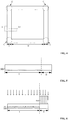
- Figure 4 shows a schematic top view of a semiconductor substrate consistent with disclosed embodiment.
- Figure 5 shows a schematic cross-section view of a portion of the semiconductor substrate along AA1 direction in Figure 4 .
- a substrate 300 is provided.
- the substrate 300 may be doped.
- the substrate 300 may further include a seal ring area I and a device area II.
- the seal ring area I may surround the device area II.
- the substrate 300 may provide a process platform for subsequent formation of device structures.
- the substrate 300 may be made of Si, Ge, SiGe, SiC, GaAs, and/or InAs.
- the substrate 300 may also be made of silicon on insulator (SOI), germanium on insulator (GOI), or any other appropriate semiconductor compound.
- SOI silicon on insulator
- GOI germanium on insulator
- the substrate 300 is made of silicon and the doping type of the substrate 300 is p-type.
- the seal ring area I may have a square shape and may include four corner regions C.
- the AA1 line may not include any of the four corner regions.
- a cross-section view of the substrate along the AA1 line is shown in Figure 5 .
- Figures 6-9 and 12 all show schematic cross-section views of semiconductor structures along the AA1 line at certain stages of the fabrication process.
- a buried deep-well layer surrounding the device area may be formed in the substrate of the seal ring area (S202).
- Figure 6 shows a schematic view of a corresponding semiconductor structure.
- a buried deep-well layer 301 is formed in the substrate 300 of the seal ring area I.
- the buried deep-well layer 301 may surround the device area II.
- the buried deep-well layer 301 may be doped.
- the doping type of the buried deep-well layer 301 may be different from the doping type of the substrate 300.
- the buried deep-well layer 301 together with a subsequently-formed well region may be used to isolate the substrate 300 of the seal ring area I from the device area II. Further, isolating the substrate 300 of the seal ring area I from other components formed in the device area II may suppress or prevent the influence of noise signal on the electrical performance of other components through the substrate 300.
- the doping ions in the substrate 300 may be p-type. Therefore, the buried deep-well layer 301 may be doped with n-type ions.
- the buried deep-well layer 301 that surrounds the device area II may be formed by performing a first ion implantation process on the substrate 300 of the seal ring area I.
- the seal ring area I may have a square shape and may include four corner regions C (shown in Figure 4 ).
- the first ion implantation process performed on the substrate 300 of the seal ring area I may include the following steps. First, a first patterned layer 901 may be formed on the surface of the substrate. The first patterned layer 901 may cover the device area II and the four corner regions C of the seal ring area I (shown in Figure 4 ). Then the first ion implantation process may be performed on the substrate 300 exposed by the first patterned layer 901 to form a buried deep-well layer 301 in the substrate of the seal ring area I. Finally, the first patterned layer 901 may be removed.
- the parameters of the first ion implantation process may include: implanting ions including phosphor ions, arsenic ions, and antimony ions; an implanting energy in a range of 100 keV to 1000 keV; and an implanting dosage in a range of 1E12 atoms/cm 2 to 1E14 atoms/cm 2 .
- the first patterned layer 901 is a photoresist layer. After forming the buried deep-well layer 301, the first patterned layer 901 may be removed by a wet etching process or an ashing process.
- a first well region surrounding the device area and a second well region surrounding the first well region may be formed in the substrate above the buried deep-well layer of the seal ring area (S203).
- Figure 7 shows a schematic view of the corresponding semiconductor structure.
- a first well region 302 may be formed in the substrate 300 above the buried deep-well layer 301 of the seal ring area I.
- the first well region 302 may surround the device area II.
- a second well region 302' may be formed in the substrate 300 above the buried deep-well layer 301 to surround the first well region 302.
- the first well region 302 and the second well region 302' may both connect with the buried deep-well layer 301 and extend to the surface of the substrate 300.
- the doping type of the first well region 302 and the second well region 302' may be different from the doping type of the substrate 300.
- the first well region 302, the second well region 302', and the buried deep-well layer 301 may form an anti-jamming barrier to isolate the substrate 300 of the seal ring area I from other components formed in the device area II. As such, influence of noise signal to the electrical performance of the components through the substrate 300 may be suppressed or prevented.
- the doping ions in the substrate 300 may be p-type. Therefore, the doping ions in the first well region 302 and the second well region 302' may be n-type.
- the formation process for the first well region 302 and the second well region 302' may include performing a second ion implantation process on the substrate 300 of the seal ring area I so that a first well region 302 surrounding the device area II and a second well region 302' surrounding the first well region 302 may be formed.
- the seal ring area I may have a square shape and may include four corner regions C (shown in Figure 4 ).
- the second ion implantation process performed on the substrate 300 of the seal ring area I may include the following steps. First, a second patterned layer 902 may be formed on the surface of the substrate 300. The second patterned layer 902 may cover the device area II and a portion of the surface of the substrate 300 in the seal ring area I including the corner regions C (shown in Figure 4 ). The second patterned layer 902 may expose only a portion of the surface of the substrate 300 above the buried deep-well layer 301.
- the second ion implantation process may be performed on the portion of the substrate 300 exposed by the second patterned layer 902 to form a first well region 302 and a second well region 302' in the substrate 300 above the buried deep-well layer 301 of the seal ring area I.
- the first well region 302 may surround the device area II while the second well region 302' may surround the first well region 302.
- the first well region 302 and the second well region 302' may both connect with the buried deep-well layer 301 and extend to the surface of the substrate 300.
- the second patterned layer 902 may be removed.
- the parameters of the second ion implantation process may include: implanting ions including phosphor ions, arsenic ions, and antimony ions; an implanting energy in a range of 100 keV to 500 keV; and an implanting dosage in a range of 5E12 atoms/cm 2 to 1E14 atoms/cm 2 .
- the second patterned layer 902 is a photoresist layer. After forming the first well region 302 and the second well region 302', the second patterned layer 902 may be removed by a wet etching process or an ashing process.
- the buried deep-well layer 301, the first well region 302, and the second well region 302' may not be formed in the corner regions C (shown in Figure 4 ) of the seal ring area I. That is, no anti-jamming barrier, which includes the buried deep-well layer 301, the first well region 302, and the second well region 302', may be formed in the corner regions C.
- the seal ring structure formed in the corner regions C may be connected to the substrate 300. Therefore, plasma may be released through the seal ring structure in the corner region C, thus damages to the devices due to accumulation of plasma may be avoided.
- a heavily doped region may be formed in the portion of the substrate surrounded by the first well region, the second well region, and the buried deep-well layer (S204).
- Figure 8 shows a schematic view of the corresponding semiconductor structure.
- a heavily doped region 303 may be formed in the portion of the substrate 300 surrounded by the first well region 302, the second well region 302', and the buried deep-well layer 301.
- the doping ions in the substrate 300 may be p-type.
- the doping ions in the heavily doped region 303 may also be p-type.
- the heavily doped region 303 may be formed by a heavy doping implantation process.
- the heavy doping implantation process may include the following steps. First, a third patterned layer 903 may be formed on the surface of the substrate 300. The third patterned layer 903 may cover the device area II, the four corner regions C (shown in Figure 4 ) of the seal ring area I, the first well region 302, and the second well region 302'. The third patterned layer 903 may expose the surface of the portion of the substrate 300 between the first well region 302 and the second well 302'. Further, a heavy doping implantation process may be performed on the portion of the substrate 300 exposed by the third patterned layer 903 to form the heavily doped region 303. Finally, the third patterned layer 903 may be removed.
- the parameters of the heavy doping implantation process may include: implanting ions including boron ions, gallium ions, and indium ions; an implanting energy in a range of 1 keV to 100 keV; and an implanting dosage in a range of 5E14 atoms/cm 2 to 1E16 atoms/cm 2 .
- the third patterned layer 903 is a photoresist layer. After forming the heavily doped region 303, the third patterned layer 903 may be removed by a wet etching process or an ashing process.
- the buried deep-well layer 301, the first well region 302, and the second well region 302' may surround the heavily doped region 303. That is, the buried deep-well layer 301, the first well region 302, and the second well region 302' together may form an anti-jamming barrier.
- the anti-jamming barrier may isolate the substrate 300 of the seal ring area I from other components formed in the device area II. Therefore, the anti-jamming barrier may prevent noise signals from entering the substrate 300 through the seal ring structure and affecting the electrical performance of the other components.
- a seal ring structure may be formed on the substrate (S205).
- Figure 9 shows a schematic view of the corresponding structure.
- a seal ring structure 400 is formed on the substrate 300.
- the seal ring structure 400 may connect with the heavily doped region 303.
- the seal ring structure 400 may be formed on the substrate 300 by a process including the following steps. First, an interlayer dielectric layer 410 may be formed on the surface of the substrate 300 in the seal ring area I. Then, a plurality of contact hole plugs 420 may be formed in the interlayer dielectric layer 410. The plurality of contact hole plugs 420 may be formed through the entire thickness of the interlayer dielectric layer 410 and may connect with the heavily doped region 303. Further, a metal interconnection layer 430 may be formed on the surface of the interlayer dielectric layer 410. The metal interconnection layer 430 may connect with the plurality of contact hole plugs 420.
- the interlayer dielectric layer 410 may have a multiple-layer structure including a first interlayer dielectric layer (not shown) formed on the substrate 300 of the seal ring area I and a second interlayer dielectric layer (not shown) formed on the first interlayer dielectric layer.
- the interlayer dielectric layer 410 may serve as an isolation structure between neighboring contact hole plugs 420.
- the interlayer dielectric layer 410 may also serve as an isolation structure between the metal interconnection layer 430 and the substrate 300.
- the first interlayer dielectric layer may be made of an insulating material such as SiO x , SiN, SiON, SiCO, SiCN, SiCON, etc.
- the first interlayer dielectric layer may be formed by a fluid chemical vapor deposition (FCVD) method; and the first interlayer dielectric layer may be made of SiO x .
- the density of the second interlayer dielectric layer may be larger than the density of the first interlayer dielectric layer.
- the second interlayer dielectric layer may be more electrically insulating as compared to the first interlayer dielectric layer so that the subsequently-formed isolation structure may have desired insulation properties.
- the second interlayer dielectric layer may be made of an insulating material such as SiO x , SiN, SiON, SiCO, SiCN, SiCNO, etc.
- the second interlayer dielectric layer may be formed by a high aspect ratio process (HARP) deposition.
- the second interlayer dielectric layer may be made of SiO x .
- the interlayer dielectric layer 410 may be formed by a process including the following steps. First, a first interlayer dielectric layer may be formed on the surface of the substrate of the seal ring area I. Then, a second interlayer dielectric film may be formed on the surface of the first interlayer dielectric layer. Finally, a planarization process may be performed on the second interlayer dielectric film to form a second interlayer dielectric layer as the thickness of the second interlayer dielectric film reaches a pre-determined value.
- HTP high aspect ratio process
- the planarization process may use a chemical mechanical polishing (CMP) method to reduce the thickness of the second interlayer dielectric film to a desired value and thus form the second interlayer dielectric layer.
- CMP chemical mechanical polishing
- the plurality of contact hole plugs 420 may be used to realize electrical connection between the substrate 300 and the metal interconnection layer 430.
- the plurality of contact hole plugs 420 may be formed by a method including the following steps. First, a patterned layer (not shown) may be formed on the surface of the interlayer dielectric layer 410. The patterned layer may contain a contact hole pattern. Then, a plurality of contact holes (not shown) may be formed by etching the interlayer dielectric layer 410 along the contact hole pattern using the patterned layer as an etch mask. Further, the plurality of contact holes may be filled with a conductive material. The conductive material may also cover the surface of the interlayer dielectric layer 410. Finally, a planarization process may be performed on the conductive material.
- the portion of the conductive material formed on the surface of the interlayer dielectric layer 410 may be removed until the conductive material formed in the interlayer dielectric layer 410 reaches a desired thickness.
- a plurality of contact hole plugs 420 may be formed through the entire thickness of the interlayer dielectric layer 410.
- the interlayer dielectric layer 410 may be etched by a plasma dry etching process to form the plurality of contact holes.
- a CMP method may be adopted to remove the portion of the conductive material formed on the surface of the interlayer dielectric layer 410 until the conductive material formed in the interlayer dielectric layer 410 reaches a desired thickness.
- the plurality of contact hole plugs 420 may be made of Cu and/or W. In one embodiment, the plurality of contact hole plugs 420 is made of W.
- the formation process for the metal interconnection layer 430 may include forming multiple metal layers 440.
- Figure 10 shows a schematic top view of the structure shown in Figure 9 from the side of the multiple metal layers 440.
- a dashed frame M in Figure 10 contains a portion of the structure.
- Figure 11 shows a zoomed-in view of the portion of the structure shown in the dashed frame M in Figure 10 .
- the formation process for each metal layer 440 may include forming multiple circles of metal lines 445 on the interlayer dielectric layer 410 to surround the device area II. Along a direction parallel to the substrate 300, a distance L (shown in Figure 11 ) between neighboring circles of the metal lines 445 may be pre-defined.
- the multiple circles of metal lines 445 of the metal layer 440 may be uniformly distributed. That is, the pre-determined distance L between different neighboring circles of the metal lines 445 may be constant.
- the multiple metal layers 440 including the multiple circles of metal lines 445 may be used to eliminate noise signals. Specifically, after noise signals from RF devices enter the seal ring structure, the noise signals may gradually diminish while passing through the multiple circles of metal lines 445. Therefore, noise signals may not be transmitted in the metal interconnection layer 430, thus the ability of the seal ring structure in resisting noise signals may be further improved.
- the pre-determined distance L may not be very small or excessively large.
- the actual fabrication process may be very difficult and neighboring circles of metal lines 445 may easily connect with each other, affecting the quality of the seal ring structure.
- the pre-determined distance L is excessively large, the number of circles allowed for metal lines 445 formed in the seal ring area I may not be large enough to efficiently eliminate noise signals.
- the pre-determined distance L is in a range of 500 ⁇ m to 1000 ⁇ m; and the number of circles of metal lines 445 formed in the seal ring area I is 4.
- the metal interconnection layer 430 may be made of Cu, W, and/or Al. In one embodiment, the metal interconnection layer 430 is made of Cu.
- the metal interconnection layer 430 may include more than one metal layers 440.
- more than one interlayer dielectric layer may be formed between neighboring metal layers 440.
- a plurality of contact hole plugs may also be formed each interlayer dielectric layer to provide electrical connection between neighboring metal layers.
- the fabrication process for the interlayer dielectric layer formed between neighboring metal layers 440 may be similar to the fabrication process for the interlayer dielectric layer 410 while the fabrication process for the plurality of contact hole plugs in each of the interlayer dielectric layer may be similar to the fabrication process for the plurality of contact hole plugs 420 formed in the interlayer dielectric layer 410.
- FIG. 12 shows a schematic cross-section view of a corresponding semiconductor structure.
- connection metal layer 500 may be formed on the surface of the seal ring structure 400. Further, the connection metal layer 500 may be connected to ground through another connection metal layer 600.
- connection metal layer 500 may be used to electrically connect different components in the seal ring region I and also connect components to external electric circuits.
- the connection metal layer 500 may be made of Al.
- connection metal layer 500 may be formed on the surface of the seal ring structure 400.
- a second passivation layer 720 may be formed on the surface of the connection metal layer 500.
- An opening (not shown) may be formed in the second passivation layer 720. The opening may expose a portion of the connection metal layer 500.
- the connection metal layer 500 may be connected to another connection metal layer 600 through the opening and the connection metal layer 600 may be grounded.
- noise signals may originate from the potential difference between a high voltage and a low voltage, by connecting the connection metal layer 500 to ground through the connection metal layer 600, potential difference in the seal ring structure 400 may be avoided. Therefore, noise signals may not be generated, thus the electrical performance of semiconductor device may be improved.
- the present invention also provides a semiconductor device.
- the semiconductor device may be formed by the fabrication method described above.
- Figure 12 shows a schematic cross-section view of a semiconductor device consistent with disclosed embodiments.
- the semiconductor device includes a substrate 300.
- the substrate 300 may include a seal ring area I and a device area II with the seal ring area I surrounding to the device area II.
- the substrate 300 may be doped.
- the semiconductor device may also include a buried deep-well layer 301.
- the buried deep-well layer 301 may be situated in the substrate 300 of the seal ring area I and may surround the device area II.
- the doping type of the buried deep-well layer 301 may be different from the doping type of the substrate 300.
- the semiconductor device may include a well region.
- the well region may be formed in the portion of the substrate 300 above the buried deep-well layer 301 of the seal ring area I.
- the well region may include a first well region 302 surrounding the device area II and a second well region 302' surrounding the first well region 302.
- the first well region 302 and the second well region 302' may both connect with the buried deep-well layer 301 and extend to the surface of the substrate 300.
- the doping type of the first well region 302 and the second well region 302' may be different from the doping type of the substrate 300.
- the semiconductor device may further include a heavily doped region 303.
- the heavily doped region 303 may be formed in the portion of the substrate 300 surrounded by the first well region 302, the second well region 302', and the buried deep-well layer 301.
- the doping type of the heavily doped region 303 may be the same as the doping type of the substrate 300.
- the semiconductor device may include a seal ring structure 400.
- the seal ring structure 400 may be formed on the substrate 300 and may connect with the heavily doped region 303.
- the substrate 300 may be doped with p-type ions.
- the buried deep-well layer 301 may be doped with n-type ions
- the first well region 302 and the second well region 302' may also be doped with n-type ions
- the heavily doped region 303 may be doped with p-type ions.
- the seal ring area I may have a square shape and may include four corner regions C (referring to Figure 4 ).
- the buried deep-well layer 301, the first well region 302, and the second well region 302' may be formed in the substrate 300 of the seal ring area I but may not be overlapped with any portion of the corner regions C.
- the seal ring structure 400 may be electrically connected to the substrate 300 at the four corner regions C. Therefore, plasma may be released through the seal ring structure at the four corner regions C, thus damages to the devices due to accumulation of plasma may be avoided.
- the seal ring structure 400 may further include an interlayer dielectric layer 410 formed on the surface of the substrate 300 of the seal ring area I, a plurality of contact hole plugs 420 formed through the entire thickness of the interlayer dielectric layer 410, and a metal interconnection layer 430 formed on the surface of the interlayer dielectric layer 410.
- the plurality of contact hole plugs 420 may connect with both the heavily doped region 303 and the metal interconnection layer 430.
- the metal interconnection layer 430 may further include multiple metal layers 440 formed on the interlayer dielectric layer 410.
- each multiple metal layer 440 may include multiple circles of metal lines 445 formed on the interlayer dielectric layer 410.
- the multiple circles of metal lines 445 may surround the device area II.
- a distance L shown in Figure 11 ) between neighboring circles of metal lines 445 may be pre-defined.
- the multiple metal layers 440 with each including multiple circles of metal lines 445 may be used to eliminate noise signals. Specifically, after noise signals from RF devices enter the seal ring structure, the noise signals may gradually diminish while passing through the multiple circles of metal lines 445. Therefore, noise signals may not be transmitted in the metal interconnection layer 430, thus the ability of the seal ring structure in resisting noise signals may be further improved.
- the multiple circles of metal lines 445 may be uniformly distributed. That is, the pre-determined distance L between different pairs of neighboring circles of the metal lines 445 of the multiple metal layers 440 may be a constant.
- the pre-determined distance L may not be very small or excessively large.
- the actual fabrication process may be very difficult and neighboring circles of metal lines 445 may easily connect with each other, affecting the quality of the seal ring structure.
- the pre-determined distance L is excessively large, the number of circles allowed for metal lines 445 formed in the seal ring area I may not be large enough to efficiently eliminate noise signals.
- the pre-determined distance L is in a range of 500 ⁇ m to 1000 ⁇ m; and the number of circles of metal lines 445 formed in the seal ring area I is 4.
- the metal interconnection layer 430 may be made of Cu, W, and/or Al. In one embodiment, the metal interconnection layer 430 is made of Cu.
- the semiconductor device may also include a connection metal layer 500 formed on the surface of the seal ring structure 400.
- the connection metal layer 500 may be connected to ground through another connection metal layer 600.
- connection metal layer 500 may be used to electrically connect different components and also connect components to external electric circuits.
- the connection metal layer 500 may be made of Al.
- connection metal layer 500 may be formed on the surface of the seal ring structure 400.
- a second passivation layer 720 may be formed on the surface of the connection metal layer 500.
- An opening (not shown) may be formed in the second passivation layer 720. The opening may expose a portion of the connection metal layer 500.
- the connection metal layer 500 may be connected to another connection metal layer 600 through the opening and the connection metal layer 600 may be grounded.
- noise signals may originate from the potential difference between a high voltage and a low voltage, by connecting the connection metal layer 500 to ground through the connection metal layer 600, potential difference in the seal ring structure 400 may be avoided. Therefore, noise signals may not be generated, thus the electrical performance of semiconductor device may be improved.
- a seal ring structure is usually formed on the substrate.
- the seal ring structure may be connected to a heavily doped region in the semiconductor device.
- Noise signal may easily enter the seal ring structure through the heavily doped region from the seal ring structure. Because the device area and the seal ring area of the semiconductor device are both on a same substrate, after entering the substrate, the noise signal may further affect the performance of other components in the semiconductor device.
- a buried deep-well layer, a first well region, and a second well region may be formed in the disclosed semiconductor device to provide an anti-jamming barrier.
- the doping type of the buried deep-well layer, the first well region, and the second well region may be different from the doping type of the substrate. Therefore, the anti-jamming barrier formed by the buried deep-well layer, the first well region, and the second well region may isolate the substrate of the seal ring area from other components formed in the device area, preventing noise signals from entering the substrate through the seal ring structure and thus affecting the electrical performance of other components.
- the seal ring structure in the semiconductor device may be capable for preventing moisture from entering the chip and also preventing ionic contamination.
- the seal ring structure may prevent the chip from damage during dicing process.
Landscapes
- Solid State Image Pick-Up Elements (AREA)
- Semiconductor Integrated Circuits (AREA)
- Physics & Mathematics (AREA)
- Health & Medical Sciences (AREA)
- Electromagnetism (AREA)
- Toxicology (AREA)
Abstract
Description
- This application claims the priority of Chinese Patent Application No.
CN201510920864.X, filed on December 11, 2015 - The present invention generally relates to the field of semiconductor fabrication technology and, more particularly, relates to a semiconductor device and fabrication methods thereof.
- Seal ring structure of semiconductor device is mainly used to protect the chip of the semiconductor device from being damaged during dicing process. Specifically, seal ring structure may prevent damages to the chip due to cracks generated by dicing blades.
- Usually, the seal ring structure is a metal shielding ring formed by overlapped contact holes, through vias, and metal layers. The seal ring structure may be formed at a position with a certain distance away from the chip, and may also keep a certain distance away from the dicing path. For different devices, the distance between the seal ring structure and the chip, and the distance between the seal ring structure and the dicing path may be different.
- In addition to providing protection for the chip during dicing process, seal ring structure may also play other roles. For example, the seal ring structure may shield noise signals coming from outside of the chip; and the seal ring structure may also prevent moisture from entering the chip through fracture surfaces on the edges.
- However, seal ring structures fabricated by existing methods may cause degradation of electrical performance of semiconductor devices. The disclosed fabrication method and semiconductor structure are directed to solve one or more problems set forth above and other problems in the art.
- A first aspect of the present invention includes a method for fabricating a semiconductor device. The method includes providing a substrate including a device area and a seal ring area surrounding the device area, and forming a buried deep-well layer in the substrate of the seal ring area to surround the device area. The buried deep-well layer has a first doping type different from a second doping type of the substrate. The method also includes forming a first well region and a second well region in the substrate above the buried deep-well layer in the seal ring area with the first well region surrounding the device area and the second well region surrounding the first well region. Each of the first well region and the second well region connects with the buried deep-well layer and extends to the surface of the substrate. In addition, each of the first well region and the second well region has the first doping type. The method further includes forming a heavily doped region in the portion of the substrate above the buried deep-well layer and between the first well region and the second well region. The heavily doped region has the second doping type. Finally, the method includes forming a seal ring structure on the substrate of the seal ring area with the seal ring structure connected to the heavily doped region.
- Preferably, the substrate is doped with p-type ions.
- Preferably, the buried deep-well layer, the first well region, and the second well region are doped with n-type ions.
- Preferably, the heavily doped region is doped with p-type ions.
- The buried deep-well layer may be formed by a first ion implantation process performed on the substrate of the seal ring area with process parameters including: implanting ions, including phosphor ions, arsenic ions, and antimony ions; an implanting energy in a range of 100 keV to 1000 keV; and an implanting dosage in a range of 1E12 atoms/cm2 to 1E14 atoms/cm2.
- Preferably the seal ring area has a square shape and includes four corner regions, and the first ion implantation process to form the buried deep-well layer includes: forming a first patterned layer on the surface of the substrate to cover the device area and the four corner regions of the seal ring area; performing the first ion implantation process on a portion of the substrate exposed by the first patterned layer to form the buried deep-well layer in the substrate; and removing the first patterned layer.
- The first well region and the second well region may be formed by a second ion implantation performed on the substrate of the seal ring area with process parameters including: implanting ions, including phosphor ions, arsenic ions, and antimony ions; an implanting energy in a range of 100 keV to 500 keV; and an implanting dosage in a range of 5E12 atoms/cm2 to 1E14 atoms/cm2.
- Preferably, the seal ring area has a square shape and includes four corner regions, and the second ion implantation process to form the first well region and the second well region includes: forming a second patterned layer on the surface of the substrate to cover the device area and a portion of the seal ring area including the four corner regions and expose only a portion of the substrate surface above the buried deep-well layer of the seal ring area; performing the second ion implantation process on the portion of the substrate exposed by the second patterned layer to form the first well region in the substrate above the buried deep-well layer to surround the seal ring area and the second well region to surround the first well region; and removing the second patterned layer.
- The heavily doped region may be formed by a heavy doping implantation process with process parameters including: implanting ions, including boron ions, gallium ions, and indium ions; an implanting energy in a range of 1 keV to 100 keV; and an implanting dosage in a range of 5E14 atoms/cm2 to 1E16 atoms/cm2.
- Preferably the seal ring area has a square shape and includes four corner regions, and the heavy doping implantation process to form the heavily doped region includes: forming a third patterned layer on the surface of the substrate to cover the device area, the four corner regions of the seal ring area, the first well region, and the second well region; performing the heavy doping implantation process on a portion of the substrate exposed by the third patterned layer to form the heavily doped region in the substrate above the buried deep-well layer; and removing the third patterned layer.
- Forming the seal ring structure on the substrate may include: forming an interlayer dielectric layer on the surface of the seal ring area; forming a plurality of contact hole plugs through an entire thickness of the interlayer dielectric layer with the plurality of contact hole plugs connected to the heavily doped region; and forming a metal interconnection layer on the surface of the interlayer dielectric layer with the metal interconnection layer connected to the plurality of contact hole plugs.
- Forming the metal interconnection layer may include: forming multiple metal layers; forming each metal layer includes forming multiple circles of metal lines to surround the device area, wherein preferably a pre-determined distance between neighboring circles of metal wires is constant; and along a direction parallel to the surface of the substrate, a distance between neighboring circles of the metal lines is pre-determined, wherein preferably the pre-determined distance is in a range of 500 µm to 1000 µm.
- After forming the seal ring structure on the surface of the substrate, a connection metal layer may be formed on a surface of the seal ring structure, and the connection metal layer may be connected to ground.
- Preferably, the connection metal layer is made of aluminum.
- A second aspect of the present invention provides a semiconductor device. The semiconductor structure includes a substrate including a device area and a seal ring area surrounding the device area, a buried deep-well layer formed in the substrate of the seal ring area to surround the device area, a first well region and a second well region formed in the substrate above the buried deep-well layer in the seal ring area with the first well region surrounding the device area and the second well region surrounding the first well region, and a heavily doped region formed in a portion of the substrate above the buried deep-well layer and between the first well region and the second well region. Each of the first well region and the second well region connects with the buried deep-well layer and extends to the surface of the substrate. The buried deep-well layer has a first doping type different from a second doping type of the substrate. Each of the first well region and the second well region has the first doping type. The heavily doped region has the second doping type. The semiconductor structure further includes a seal ring structure formed on the substrate of the seal ring area with the seal ring structure connected to the heavily doped region.
- Preferably, the substrate is doped with p-type ions.
- Preferably, the buried deep-well layer, the first well region, and the second well region are doped with n-type ions.
- Preferably, the heavily doped region is doped with p-type ions.
- The seal ring structure may further includes: an interlayer dielectric layer formed on the surface of the seal ring area; a plurality of contact hole plugs formed through an entire thickness of the interlayer dielectric layer with the plurality of contact hole plugs connected to the heavily doped region; and a metal interconnection layer formed on the surface of the interlayer dielectric layer with the metal interconnection layer connected to the plurality of contact hole plugs.
- The metal interconnection layer may include multiple metal layers.
- Each metal layer may include multiple circles of metal surrounding the device area.
- Along a direction parallel to the surface of the substrate, a distance between neighboring circles of the metal lines may be pre-determined. Preferably, the pre-determined distance is in a range of 500 µm to 1000 µm.
- The semiconductor device may further include a grounded connection metal layer formed on a surface of the seal ring structure.
- Other aspects of the present invention can be understood by those skilled in the art in light of the description, the claims, and the drawings of the present invention.
- The following drawings are merely examples for illustrative purposes according to various disclosed embodiments and are not intended to limit the scope of the present invention which is defined in the claims.
-
Figures 1-3 illustrate schematic views of semiconductor structures corresponding to certain stages of an existing fabrication method; -
Figures 4-12 illustrate schematic views of semiconductor structures corresponding to certain stages of an exemplary fabrication method consistent with disclosed embodiments; and -
Figure 13 illustrates a flowchart of the exemplary fabrication process consistent with disclosed embodiments. - Reference will now be made in detail to exemplary embodiments of the invention, which are illustrated in the accompanying drawings. Wherever possible, the same reference numbers will be used throughout the drawings to refer to the same or like parts.
-
Figures 1-3 show schematic views of semiconductor structures corresponding to certain stages according to an existing fabrication method. The existing fabrication method includes the following steps. First, as shown inFigure 1 , asubstrate 100 is provided. Thesubstrate 100 includes a seal ring area I and a device area II. The seal ring area I surrounds the device area II. A heavily dopedregion 101 is formed in thesubstrate 100 of the seal ring area I. The type of ions doped in the heavily dopedregion 101 is the same as the type of ions doped in thesubstrate 100. Further, as shown inFigure 2 , after forming the heavily dopedregion 101, aseal ring structure 200 is formed on thesubstrate 100 of the seal ring area I. Finally, referring toFigure 3 , afirst passivation layer 210, aconnection metal layer 220, and a second passivation layer 230 are sequentially formed on the surface of theseal ring structure 200. Specifically, the second passivation layer 230 covers theconnection metal layer 220, and theconnection metal layer 220 is not electrically grounded. - Radio frequency (RF) device is usually located in the seal ring area I, which may surround the device area II. The RF device may include noise-generating components such as inductors and capacitors. Further, the doping type of the heavily doped
region 101 may be the same as the doping type of thesubstrate 100. That is, the heavily dopedregion 101 may be connected to thesubstrate 100 of the seal ring area I and the device area II, and the seal ring area I may be defined on asame substrate 100. Therefore, when the inductors and capacitors are close to the seal ring area I and the device area II, noise signals generated by RF devices may easily enter thesubstrate 100 through theseal ring structure 200, and thus may affect the electrical performance of other electronic components. - The present invention provides a method for fabricating a semiconductor structure.
Figure 13 shows a flowchart of an exemplary fabrication method consistent with disclosed embodiments.Figures 4-12 show schematic views of semiconductor structures corresponding to certain stages of the exemplary fabrication method. - Referring to
Figure 13 , at the beginning of the fabrication process, a substrate including a device area and a seal ring area is provided (S201).Figure 4 shows a schematic top view of a semiconductor substrate consistent with disclosed embodiment.Figure 5 shows a schematic cross-section view of a portion of the semiconductor substrate along AA1 direction inFigure 4 . - Referring to
Figure 4 and Figure 5 , asubstrate 300 is provided. Thesubstrate 300 may be doped. Thesubstrate 300 may further include a seal ring area I and a device area II. The seal ring area I may surround the device area II. - The
substrate 300 may provide a process platform for subsequent formation of device structures. Thesubstrate 300 may be made of Si, Ge, SiGe, SiC, GaAs, and/or InAs. Thesubstrate 300 may also be made of silicon on insulator (SOI), germanium on insulator (GOI), or any other appropriate semiconductor compound. In one embodiment, thesubstrate 300 is made of silicon and the doping type of thesubstrate 300 is p-type. - Referring to
Figure 4 , the seal ring area I may have a square shape and may include four corner regions C. The AA1 line may not include any of the four corner regions. A cross-section view of the substrate along the AA1 line is shown inFigure 5 . Further,Figures 6-9 and12 all show schematic cross-section views of semiconductor structures along the AA1 line at certain stages of the fabrication process. - Returning to
Figure 13 , further, a buried deep-well layer surrounding the device area may be formed in the substrate of the seal ring area (S202).Figure 6 shows a schematic view of a corresponding semiconductor structure. - Referring to
Figure 6 , a buried deep-well layer 301 is formed in thesubstrate 300 of the seal ring area I. The buried deep-well layer 301 may surround the device area II. The buried deep-well layer 301 may be doped. The doping type of the buried deep-well layer 301 may be different from the doping type of thesubstrate 300. - The buried deep-
well layer 301 together with a subsequently-formed well region may be used to isolate thesubstrate 300 of the seal ring area I from the device area II. Further, isolating thesubstrate 300 of the seal ring area I from other components formed in the device area II may suppress or prevent the influence of noise signal on the electrical performance of other components through thesubstrate 300. - In one embodiment, the doping ions in the
substrate 300 may be p-type. Therefore, the buried deep-well layer 301 may be doped with n-type ions. The buried deep-well layer 301 that surrounds the device area II may be formed by performing a first ion implantation process on thesubstrate 300 of the seal ring area I. - Specifically, the seal ring area I may have a square shape and may include four corner regions C (shown in
Figure 4 ). The first ion implantation process performed on thesubstrate 300 of the seal ring area I may include the following steps. First, a firstpatterned layer 901 may be formed on the surface of the substrate. The firstpatterned layer 901 may cover the device area II and the four corner regions C of the seal ring area I (shown inFigure 4 ). Then the first ion implantation process may be performed on thesubstrate 300 exposed by the first patternedlayer 901 to form a buried deep-well layer 301 in the substrate of the seal ring area I. Finally, the first patternedlayer 901 may be removed. - In one embodiment, the parameters of the first ion implantation process may include: implanting ions including phosphor ions, arsenic ions, and antimony ions; an implanting energy in a range of 100 keV to 1000 keV; and an implanting dosage in a range of 1E12 atoms/cm2 to 1E14 atoms/cm2.
- In one embodiment, the first patterned
layer 901 is a photoresist layer. After forming the buried deep-well layer 301, the first patternedlayer 901 may be removed by a wet etching process or an ashing process. - Further, returning to
Figure 13 , a first well region surrounding the device area and a second well region surrounding the first well region may be formed in the substrate above the buried deep-well layer of the seal ring area (S203).Figure 7 shows a schematic view of the corresponding semiconductor structure. - Referring to
Figure 7 , afirst well region 302 may be formed in thesubstrate 300 above the buried deep-well layer 301 of the seal ring area I. Thefirst well region 302 may surround the device area II. A second well region 302' may be formed in thesubstrate 300 above the buried deep-well layer 301 to surround thefirst well region 302. Thefirst well region 302 and the second well region 302' may both connect with the buried deep-well layer 301 and extend to the surface of thesubstrate 300. The doping type of thefirst well region 302 and the second well region 302' may be different from the doping type of thesubstrate 300. - The
first well region 302, the second well region 302', and the buried deep-well layer 301 may form an anti-jamming barrier to isolate thesubstrate 300 of the seal ring area I from other components formed in the device area II. As such, influence of noise signal to the electrical performance of the components through thesubstrate 300 may be suppressed or prevented. - In one embodiment, the doping ions in the
substrate 300 may be p-type. Therefore, the doping ions in thefirst well region 302 and the second well region 302' may be n-type. The formation process for thefirst well region 302 and the second well region 302' may include performing a second ion implantation process on thesubstrate 300 of the seal ring area I so that afirst well region 302 surrounding the device area II and a second well region 302' surrounding thefirst well region 302 may be formed. - Specifically, the seal ring area I may have a square shape and may include four corner regions C (shown in
Figure 4 ). The second ion implantation process performed on thesubstrate 300 of the seal ring area I may include the following steps. First, a secondpatterned layer 902 may be formed on the surface of thesubstrate 300. The secondpatterned layer 902 may cover the device area II and a portion of the surface of thesubstrate 300 in the seal ring area I including the corner regions C (shown inFigure 4 ). The secondpatterned layer 902 may expose only a portion of the surface of thesubstrate 300 above the buried deep-well layer 301. Then, the second ion implantation process may be performed on the portion of thesubstrate 300 exposed by the secondpatterned layer 902 to form afirst well region 302 and a second well region 302' in thesubstrate 300 above the buried deep-well layer 301 of the seal ring area I. Thefirst well region 302 may surround the device area II while the second well region 302' may surround thefirst well region 302. Thefirst well region 302 and the second well region 302' may both connect with the buried deep-well layer 301 and extend to the surface of thesubstrate 300. Finally, the secondpatterned layer 902 may be removed. - In one embodiment, the parameters of the second ion implantation process may include: implanting ions including phosphor ions, arsenic ions, and antimony ions; an implanting energy in a range of 100 keV to 500 keV; and an implanting dosage in a range of 5E12 atoms/cm2 to 1E14 atoms/cm2.
- In one embodiment, the second
patterned layer 902 is a photoresist layer. After forming thefirst well region 302 and the second well region 302', the secondpatterned layer 902 may be removed by a wet etching process or an ashing process. - Specifically, the buried deep-
well layer 301, thefirst well region 302, and the second well region 302' may not be formed in the corner regions C (shown inFigure 4 ) of the seal ring area I. That is, no anti-jamming barrier, which includes the buried deep-well layer 301, thefirst well region 302, and the second well region 302', may be formed in the corner regions C. The seal ring structure formed in the corner regions C may be connected to thesubstrate 300. Therefore, plasma may be released through the seal ring structure in the corner region C, thus damages to the devices due to accumulation of plasma may be avoided. - Further, returning to
Figure 13 , a heavily doped region may be formed in the portion of the substrate surrounded by the first well region, the second well region, and the buried deep-well layer (S204).Figure 8 shows a schematic view of the corresponding semiconductor structure. - Referring to
Figure 8 , a heavily dopedregion 303 may be formed in the portion of thesubstrate 300 surrounded by thefirst well region 302, the second well region 302', and the buried deep-well layer 301. - In one embodiment, the doping ions in the
substrate 300 may be p-type. Correspondingly, the doping ions in the heavily dopedregion 303 may also be p-type. The heavily dopedregion 303 may be formed by a heavy doping implantation process. - Specifically, the heavy doping implantation process may include the following steps. First, a third
patterned layer 903 may be formed on the surface of thesubstrate 300. The thirdpatterned layer 903 may cover the device area II, the four corner regions C (shown inFigure 4 ) of the seal ring area I, thefirst well region 302, and the second well region 302'. The thirdpatterned layer 903 may expose the surface of the portion of thesubstrate 300 between thefirst well region 302 and the second well 302'. Further, a heavy doping implantation process may be performed on the portion of thesubstrate 300 exposed by the thirdpatterned layer 903 to form the heavily dopedregion 303. Finally, the thirdpatterned layer 903 may be removed. - In one embodiment, the parameters of the heavy doping implantation process may include: implanting ions including boron ions, gallium ions, and indium ions; an implanting energy in a range of 1 keV to 100 keV; and an implanting dosage in a range of 5E14 atoms/cm2 to 1E16 atoms/cm2.
- In one embodiment, the third
patterned layer 903 is a photoresist layer. After forming the heavily dopedregion 303, the thirdpatterned layer 903 may be removed by a wet etching process or an ashing process. - Specifically, the buried deep-
well layer 301, thefirst well region 302, and the second well region 302' may surround the heavily dopedregion 303. That is, the buried deep-well layer 301, thefirst well region 302, and the second well region 302' together may form an anti-jamming barrier. As the doping type of the buried deep-well layer 301, thefirst well region 302, and the second well region 302' may be different from the doping type of thesubstrate 300, the anti-jamming barrier may isolate thesubstrate 300 of the seal ring area I from other components formed in the device area II. Therefore, the anti-jamming barrier may prevent noise signals from entering thesubstrate 300 through the seal ring structure and affecting the electrical performance of the other components. - Further, returning to
Figure 13 , a seal ring structure may be formed on the substrate (S205).Figure 9 shows a schematic view of the corresponding structure. - Referring to
Figure 9 , aseal ring structure 400 is formed on thesubstrate 300. Theseal ring structure 400 may connect with the heavily dopedregion 303. - In one embodiment, the
seal ring structure 400 may be formed on thesubstrate 300 by a process including the following steps. First, aninterlayer dielectric layer 410 may be formed on the surface of thesubstrate 300 in the seal ring area I. Then, a plurality of contact hole plugs 420 may be formed in theinterlayer dielectric layer 410. The plurality of contact hole plugs 420 may be formed through the entire thickness of theinterlayer dielectric layer 410 and may connect with the heavily dopedregion 303. Further, ametal interconnection layer 430 may be formed on the surface of theinterlayer dielectric layer 410. Themetal interconnection layer 430 may connect with the plurality of contact hole plugs 420. - In one embodiment, the
interlayer dielectric layer 410 may have a multiple-layer structure including a first interlayer dielectric layer (not shown) formed on thesubstrate 300 of the seal ring area I and a second interlayer dielectric layer (not shown) formed on the first interlayer dielectric layer. - The
interlayer dielectric layer 410 may serve as an isolation structure between neighboring contact hole plugs 420. Theinterlayer dielectric layer 410 may also serve as an isolation structure between themetal interconnection layer 430 and thesubstrate 300. - The first interlayer dielectric layer may be made of an insulating material such as SiOx, SiN, SiON, SiCO, SiCN, SiCON, etc. In one embodiment, the first interlayer dielectric layer may be formed by a fluid chemical vapor deposition (FCVD) method; and the first interlayer dielectric layer may be made of SiOx.
- The density of the second interlayer dielectric layer may be larger than the density of the first interlayer dielectric layer. The second interlayer dielectric layer may be more electrically insulating as compared to the first interlayer dielectric layer so that the subsequently-formed isolation structure may have desired insulation properties. The second interlayer dielectric layer may be made of an insulating material such as SiOx, SiN, SiON, SiCO, SiCN, SiCNO, etc.
- In one embodiment, the second interlayer dielectric layer may be formed by a high aspect ratio process (HARP) deposition. The second interlayer dielectric layer may be made of SiOx. Specifically, the
interlayer dielectric layer 410 may be formed by a process including the following steps. First, a first interlayer dielectric layer may be formed on the surface of the substrate of the seal ring area I. Then, a second interlayer dielectric film may be formed on the surface of the first interlayer dielectric layer. Finally, a planarization process may be performed on the second interlayer dielectric film to form a second interlayer dielectric layer as the thickness of the second interlayer dielectric film reaches a pre-determined value. - In one embodiment, the planarization process may use a chemical mechanical polishing (CMP) method to reduce the thickness of the second interlayer dielectric film to a desired value and thus form the second interlayer dielectric layer.
- The plurality of contact hole plugs 420 may be used to realize electrical connection between the
substrate 300 and themetal interconnection layer 430. - Specifically, the plurality of contact hole plugs 420 may be formed by a method including the following steps. First, a patterned layer (not shown) may be formed on the surface of the
interlayer dielectric layer 410. The patterned layer may contain a contact hole pattern. Then, a plurality of contact holes (not shown) may be formed by etching theinterlayer dielectric layer 410 along the contact hole pattern using the patterned layer as an etch mask. Further, the plurality of contact holes may be filled with a conductive material. The conductive material may also cover the surface of theinterlayer dielectric layer 410. Finally, a planarization process may be performed on the conductive material. Specifically, the portion of the conductive material formed on the surface of theinterlayer dielectric layer 410 may be removed until the conductive material formed in theinterlayer dielectric layer 410 reaches a desired thickness. As such, a plurality of contact hole plugs 420 may be formed through the entire thickness of theinterlayer dielectric layer 410. - In one embodiment, the
interlayer dielectric layer 410 may be etched by a plasma dry etching process to form the plurality of contact holes. In addition, a CMP method may be adopted to remove the portion of the conductive material formed on the surface of theinterlayer dielectric layer 410 until the conductive material formed in theinterlayer dielectric layer 410 reaches a desired thickness. - The plurality of contact hole plugs 420 may be made of Cu and/or W. In one embodiment, the plurality of contact hole plugs 420 is made of W.
- Further, the formation process for the
metal interconnection layer 430 may include forming multiple metal layers 440. -
Figure 10 shows a schematic top view of the structure shown inFigure 9 from the side of the multiple metal layers 440. A dashed frame M inFigure 10 contains a portion of the structure.Figure 11 shows a zoomed-in view of the portion of the structure shown in the dashed frame M inFigure 10 . The formation process for eachmetal layer 440 may include forming multiple circles ofmetal lines 445 on theinterlayer dielectric layer 410 to surround the device area II. Along a direction parallel to thesubstrate 300, a distance L (shown inFigure 11 ) between neighboring circles of themetal lines 445 may be pre-defined. - In one embodiment, the multiple circles of
metal lines 445 of themetal layer 440 may be uniformly distributed. That is, the pre-determined distance L between different neighboring circles of themetal lines 445 may be constant. - The
multiple metal layers 440 including the multiple circles ofmetal lines 445 may be used to eliminate noise signals. Specifically, after noise signals from RF devices enter the seal ring structure, the noise signals may gradually diminish while passing through the multiple circles ofmetal lines 445. Therefore, noise signals may not be transmitted in themetal interconnection layer 430, thus the ability of the seal ring structure in resisting noise signals may be further improved. - Moreover, the pre-determined distance L may not be very small or excessively large. When the pre-determined distance L is too small, the actual fabrication process may be very difficult and neighboring circles of
metal lines 445 may easily connect with each other, affecting the quality of the seal ring structure. On the other hand, when the pre-determined distance L is excessively large, the number of circles allowed formetal lines 445 formed in the seal ring area I may not be large enough to efficiently eliminate noise signals. In one embodiment, the pre-determined distance L is in a range of 500 µm to 1000 µm; and the number of circles ofmetal lines 445 formed in the seal ring area I is 4. - The
metal interconnection layer 430 may be made of Cu, W, and/or Al. In one embodiment, themetal interconnection layer 430 is made of Cu. - In one embodiment, the
metal interconnection layer 430 may include more than one metal layers 440. Correspondingly, referring toFigure 9 , more than one interlayer dielectric layer may be formed between neighboring metal layers 440. In addition, a plurality of contact hole plugs may also be formed each interlayer dielectric layer to provide electrical connection between neighboring metal layers. The fabrication process for the interlayer dielectric layer formed between neighboringmetal layers 440 may be similar to the fabrication process for theinterlayer dielectric layer 410 while the fabrication process for the plurality of contact hole plugs in each of the interlayer dielectric layer may be similar to the fabrication process for the plurality of contact hole plugs 420 formed in theinterlayer dielectric layer 410. - Further, returning to
Figure 13 , after forming the seal ring structure, a connection metal layer may be formed on the surface of the seal ring structure.Figure 12 shows a schematic cross-section view of a corresponding semiconductor structure. - Referring to
Figure 12 , aconnection metal layer 500 may be formed on the surface of theseal ring structure 400. Further, theconnection metal layer 500 may be connected to ground through anotherconnection metal layer 600. - The
connection metal layer 500 may be used to electrically connect different components in the seal ring region I and also connect components to external electric circuits. In one embodiment, theconnection metal layer 500 may be made of Al. - Further, prior to the formation of the
connection metal layer 500 on the surface of theseal ring structure 400, the fabrication method may also include the following steps. First, a second passivation layer 720 may be formed on the surface of theconnection metal layer 500. An opening (not shown) may be formed in the second passivation layer 720. The opening may expose a portion of theconnection metal layer 500. Finally, theconnection metal layer 500 may be connected to anotherconnection metal layer 600 through the opening and theconnection metal layer 600 may be grounded. - Because noise signals may originate from the potential difference between a high voltage and a low voltage, by connecting the
connection metal layer 500 to ground through theconnection metal layer 600, potential difference in theseal ring structure 400 may be avoided. Therefore, noise signals may not be generated, thus the electrical performance of semiconductor device may be improved. - The present invention also provides a semiconductor device. The semiconductor device may be formed by the fabrication method described above.
Figure 12 shows a schematic cross-section view of a semiconductor device consistent with disclosed embodiments. - Referring to
Figure 12 , the semiconductor device includes asubstrate 300. Thesubstrate 300 may include a seal ring area I and a device area II with the seal ring area I surrounding to the device area II. Thesubstrate 300 may be doped. - The semiconductor device may also include a buried deep-
well layer 301. The buried deep-well layer 301 may be situated in thesubstrate 300 of the seal ring area I and may surround the device area II. The doping type of the buried deep-well layer 301 may be different from the doping type of thesubstrate 300. - In addition, the semiconductor device may include a well region. The well region may be formed in the portion of the
substrate 300 above the buried deep-well layer 301 of the seal ring area I. The well region may include afirst well region 302 surrounding the device area II and a second well region 302' surrounding thefirst well region 302. Thefirst well region 302 and the second well region 302' may both connect with the buried deep-well layer 301 and extend to the surface of thesubstrate 300. The doping type of thefirst well region 302 and the second well region 302' may be different from the doping type of thesubstrate 300. - The semiconductor device may further include a heavily doped
region 303. The heavily dopedregion 303 may be formed in the portion of thesubstrate 300 surrounded by thefirst well region 302, the second well region 302', and the buried deep-well layer 301. In addition, the doping type of the heavily dopedregion 303 may be the same as the doping type of thesubstrate 300. - Finally, the semiconductor device may include a
seal ring structure 400. Theseal ring structure 400 may be formed on thesubstrate 300 and may connect with the heavily dopedregion 303. - In one embodiment, the
substrate 300 may be doped with p-type ions. Correspondingly, the buried deep-well layer 301 may be doped with n-type ions, thefirst well region 302 and the second well region 302' may also be doped with n-type ions, and the heavily dopedregion 303 may be doped with p-type ions. - The seal ring area I may have a square shape and may include four corner regions C (referring to
Figure 4 ). The buried deep-well layer 301, thefirst well region 302, and the second well region 302' may be formed in thesubstrate 300 of the seal ring area I but may not be overlapped with any portion of the corner regions C. Theseal ring structure 400 may be electrically connected to thesubstrate 300 at the four corner regions C. Therefore, plasma may be released through the seal ring structure at the four corner regions C, thus damages to the devices due to accumulation of plasma may be avoided. - In one embodiment, the
seal ring structure 400 may further include aninterlayer dielectric layer 410 formed on the surface of thesubstrate 300 of the seal ring area I, a plurality of contact hole plugs 420 formed through the entire thickness of theinterlayer dielectric layer 410, and ametal interconnection layer 430 formed on the surface of theinterlayer dielectric layer 410. The plurality of contact hole plugs 420 may connect with both the heavily dopedregion 303 and themetal interconnection layer 430. - Further, the
metal interconnection layer 430 may further includemultiple metal layers 440 formed on theinterlayer dielectric layer 410. Referring toFigure 10 and Figure 11 , eachmultiple metal layer 440 may include multiple circles ofmetal lines 445 formed on theinterlayer dielectric layer 410. The multiple circles ofmetal lines 445 may surround the device area II. In addition, along a direction parallel to thesubstrate 300, a distance L (shown inFigure 11 ) between neighboring circles ofmetal lines 445 may be pre-defined. - The
multiple metal layers 440 with each including multiple circles ofmetal lines 445 may be used to eliminate noise signals. Specifically, after noise signals from RF devices enter the seal ring structure, the noise signals may gradually diminish while passing through the multiple circles ofmetal lines 445. Therefore, noise signals may not be transmitted in themetal interconnection layer 430, thus the ability of the seal ring structure in resisting noise signals may be further improved. - In one embodiment, the multiple circles of
metal lines 445 may be uniformly distributed. That is, the pre-determined distance L between different pairs of neighboring circles of themetal lines 445 of themultiple metal layers 440 may be a constant. - Moreover, the pre-determined distance L may not be very small or excessively large. When the pre-determined distance L is too small, the actual fabrication process may be very difficult and neighboring circles of
metal lines 445 may easily connect with each other, affecting the quality of the seal ring structure. On the other hand, when the pre-determined distance L is excessively large, the number of circles allowed formetal lines 445 formed in the seal ring area I may not be large enough to efficiently eliminate noise signals. In one embodiment, the pre-determined distance L is in a range of 500 µm to 1000 µm; and the number of circles ofmetal lines 445 formed in the seal ring area I is 4. - The
metal interconnection layer 430 may be made of Cu, W, and/or Al. In one embodiment, themetal interconnection layer 430 is made of Cu. - Moreover, the semiconductor device may also include a
connection metal layer 500 formed on the surface of theseal ring structure 400. Theconnection metal layer 500 may be connected to ground through anotherconnection metal layer 600. - The
connection metal layer 500 may be used to electrically connect different components and also connect components to external electric circuits. In one embodiment, theconnection metal layer 500 may be made of Al. - Further, prior to the formation of the
connection metal layer 500 on the surface of theseal ring structure 400, the fabrication method may also include the following steps. First, a second passivation layer 720 may be formed on the surface of theconnection metal layer 500. An opening (not shown) may be formed in the second passivation layer 720. The opening may expose a portion of theconnection metal layer 500. Finally, theconnection metal layer 500 may be connected to anotherconnection metal layer 600 through the opening and theconnection metal layer 600 may be grounded. - Because noise signals may originate from the potential difference between a high voltage and a low voltage, by connecting the
connection metal layer 500 to ground through theconnection metal layer 600, potential difference in theseal ring structure 400 may be avoided. Therefore, noise signals may not be generated, thus the electrical performance of semiconductor device may be improved. - According to existing semiconductor device and the fabrication method, a seal ring structure is usually formed on the substrate. The seal ring structure may be connected to a heavily doped region in the semiconductor device. Noise signal may easily enter the seal ring structure through the heavily doped region from the seal ring structure. Because the device area and the seal ring area of the semiconductor device are both on a same substrate, after entering the substrate, the noise signal may further affect the performance of other components in the semiconductor device.
- According to the disclosed semiconductor device and the fabrication method, a buried deep-well layer, a first well region, and a second well region may be formed in the disclosed semiconductor device to provide an anti-jamming barrier. Further, the doping type of the buried deep-well layer, the first well region, and the second well region may be different from the doping type of the substrate. Therefore, the anti-jamming barrier formed by the buried deep-well layer, the first well region, and the second well region may isolate the substrate of the seal ring area from other components formed in the device area, preventing noise signals from entering the substrate through the seal ring structure and thus affecting the electrical performance of other components.
- In addition, according to the disclosed semiconductor device and the fabrication method, the seal ring structure in the semiconductor device may be capable for preventing moisture from entering the chip and also preventing ionic contamination. Moreover, the seal ring structure may prevent the chip from damage during dicing process.
Claims (15)
- A method for fabricating a semiconductor device, comprising:providing a substrate including a device area and a seal ring area surrounding the device area;forming a buried deep-well layer in the substrate of the seal ring area to surround the device area, wherein the buried deep-well layer has a first doping type different from a second doping type of the substrate;forming a first well region and a second well region in the substrate above the buried deep-well layer in the seal ring area with the first well region surrounding the device area and the second well region surrounding the first well region,wherein each of the first well region and the second well region connects with the buried deep-well layer and extends to a surface of the substrate, and each of the first well region and the second well region has the first doping type;forming a heavily doped region in a portion of the substrate above the buried deep-well layer and between the first well region and the second well region, wherein the heavily doped region has the second doping type; andforming a seal ring structure on the substrate of the seal ring area with the seal ring structure connected to the heavily doped region.
- The method for fabricating the semiconductor device according to claim 1, wherein:the substrate is doped with p-type ions;the buried deep-well layer, the first well region, and the second well region are doped with n-type ions; andthe heavily doped region is doped with p-type ions.
- The method for fabricating the semiconductor device according to claim 1 or 2,
wherein the buried deep-well layer is formed by a first ion implantation process performed on the substrate of the seal ring area with process parameters including: implanting ions, including phosphor ions, arsenic ions, and antimony ions; an implanting energy in a range of 100 keV to 1000 keV; and an implanting dosage in a range of 1E12 atoms/cm2 to 1E14 atoms/cm2 ; and
wherein preferably the seal ring area has a square shape and includes four corner regions, and the first ion implantation process to form the buried deep-well layer includes:forming a first patterned layer on the surface of the substrate to cover the device area and the four corner regions of the seal ring area; performing the first ion implantation process on a portion of the substrate exposed by the first patterned layer to form the buried deep-well layer in the substrate; and removing the first patterned layer. - The method for fabricating the semiconductor device according to any one of the claims 1-3,
wherein the first well region and the second well region are formed by a second ion implantation performed on the substrate of the seal ring area with process parameters including: implanting ions, including phosphor ions, arsenic ions, and antimony ions; an implanting energy in a range of 100 keV to 500 keV; and an implanting dosage in a range of 5E12 atoms/cm2 to 1E14 atoms/cm2; and
wherein preferably the seal ring area has a square shape and includes four corner regions, and the second ion implantation process to form the first well region and the second well region includes: forming a second patterned layer on the surface of the substrate to cover the device area and a portion of the seal ring area including the four corner regions and expose only a portion of the substrate surface above the buried deep-well layer of the seal ring area; performing the second ion implantation process on the portion of the substrate exposed by the second patterned layer to form the first well region in the substrate above the buried deep-well layer to surround the seal ring area and the second well region to surround the first well region; and removing the second patterned layer. - The method for fabricating the semiconductor device according to any one of the claims 1-4, wherein the heavily doped region is formed by a heavy doping implantation process with process parameters including: implanting ions, including boron ions, gallium ions, and indium ions; an implanting energy in a range of 1 keV to 100 keV; and an implanting dosage in a range of 5E14 atoms/cm2 to 1E16 atoms/cm2.
wherein preferably the seal ring area has a square shape and includes four corner regions, and the heavy doping implantation process to form the heavily doped region includes:forming a third patterned layer on the surface of the substrate to cover the device area, the four corner regions of the seal ring area, the first well region, and the second well region;performing the heavy doping implantation process on a portion of the substrate exposed by the third patterned layer to form the heavily doped region in the substrate above the buried deep-well layer; and removing the third patterned layer. - The method for fabricating the semiconductor device according to any one of the claims 1-5, wherein forming the seal ring structure on the substrate includes:forming an interlayer dielectric layer on the surface of the seal ring area;forming a plurality of contact hole plugs through an entire thickness of the interlayer dielectric layer with the plurality of contact hole plugs connected to the heavily doped region; andforming a metal interconnection layer on the surface of the interlayer dielectric layer with the metal interconnection layer connected to the plurality of contact hole plugs.
- The method for fabricating the semiconductor device according to claim 6, wherein:forming the metal interconnection layer includes forming multiple metal layers;forming each metal layer includes forming multiple circles of metal lines to surround the device area, wherein preferably a pre-determined distance between neighboring circles of metal wires is constant; andalong a direction parallel to the surface of the substrate, a distance between neighboring circles of the metal lines is pre-determined, wherein preferably the pre-determined distance is in a range of 500 µm to 1000 µm.
- The method for fabricating the semiconductor device according to any one of the claims 1-7, after forming the seal ring structure on the surface of the substrate, further including:forming a connection metal layer on a surface of the seal ring structure; andconnecting the connection metal layer to ground.
- The method for fabricating the semiconductor device according to claim 8, wherein the connection metal layer is made of aluminum.
- A semiconductor device, comprising:a substrate including a device area and a seal ring area surrounding the device area;a buried deep-well layer formed in the substrate of the seal ring area to surround the device area, wherein the buried deep-well layer has a first doping type different from a second doping type of the substrate;a first well region and a second well region formed in the substrate above the buried deep-well layer in the seal ring area with the first well region surrounding the device area and the second well region surrounding the first well region,wherein each of the first well region and the second well region connects with the buried deep-well layer and extends to a surface of the substrate, and each of the first well region and the second well region has the first doping type;a heavily doped region formed in a portion of the substrate above the buried deep-well layer and between the first well region and the second well region, wherein the heavily doped region has the second doping type; anda seal ring structure formed on the substrate of the seal ring area with the seal ring structure connected to the heavily doped region.
- The semiconductor device according to claim 10, wherein:the substrate is doped with p-type ions;the buried deep-well layer, the first well region, and the second well region are doped with n-type ions; andthe heavily doped region is doped with p-type ions.
- The semiconductor device according to claim 10 or 11, wherein the seal ring structure further includes:an interlayer dielectric layer formed on the surface of the seal ring area;a plurality of contact hole plugs formed through an entire thickness of the interlayer dielectric layer with the plurality of contact hole plugs connected to the heavily doped region; anda metal interconnection layer formed on the surface of the interlayer dielectric layer with the metal interconnection layer connected to the plurality of contact hole plugs.
- The semiconductor device according to claim 12, wherein:the metal interconnection layer includes multiple metal layers;each metal layer includes multiple circles of metal surrounding the device area; andalong a direction parallel to the surface of the substrate, a distance between neighboring circles of the metal lines is pre-determined.
- The semiconductor device according to claim 13, wherein the pre-determined distance is in a range of 500 µm to 1000 µm.
- The semiconductor device according to any one of the claims 10-14, further including a grounded connection metal layer formed on a surface of the seal ring structure.
Applications Claiming Priority (1)
| Application Number | Priority Date | Filing Date | Title |
|---|---|---|---|
| CN201510920864.XA CN106876318B (en) | 2015-12-11 | 2015-12-11 | Semiconductor device and method for manufacturing the same |
Publications (2)
| Publication Number | Publication Date |
|---|---|
| EP3179511A1 true EP3179511A1 (en) | 2017-06-14 |
| EP3179511B1 EP3179511B1 (en) | 2020-01-01 |
Family
ID=57394424
Family Applications (1)
| Application Number | Title | Priority Date | Filing Date |
|---|---|---|---|
| EP16200266.1A Active EP3179511B1 (en) | 2015-12-11 | 2016-11-23 | Semiconductor device and fabrication method thereof |
Country Status (3)
| Country | Link |
|---|---|
| US (1) | US10032860B2 (en) |
| EP (1) | EP3179511B1 (en) |
| CN (1) | CN106876318B (en) |
Families Citing this family (4)
| Publication number | Priority date | Publication date | Assignee | Title |
|---|---|---|---|---|
| US9793227B1 (en) * | 2016-04-21 | 2017-10-17 | Peregrine Semiconductor San Diego | Switchable die seal connection |
| WO2018040100A1 (en) * | 2016-09-05 | 2018-03-08 | 飞昂通讯科技南通有限公司 | Anti-interference semiconductor device for optical transceiver |
| CN109545841A (en) * | 2018-11-22 | 2019-03-29 | 长江存储科技有限责任公司 | Double guard ring and method of forming the same |
| CN114628368B (en) * | 2022-03-10 | 2022-11-11 | 深圳市赛元微电子股份有限公司 | Electromagnetic shielding device of chip circuit module |
Citations (2)
| Publication number | Priority date | Publication date | Assignee | Title |
|---|---|---|---|---|
| US20090243052A1 (en) * | 2008-03-26 | 2009-10-01 | Maxrise Inc. | Electronic device with shielding structure and method of manufacturing the same |
| US20120104594A1 (en) * | 2010-10-29 | 2012-05-03 | Taiwan Semiconductor Manufacturing Company, Ltd. | Grounded seal ring structure in semiconductor devices |
Family Cites Families (6)
| Publication number | Priority date | Publication date | Assignee | Title |
|---|---|---|---|---|
| JP4689244B2 (en) * | 2004-11-16 | 2011-05-25 | ルネサスエレクトロニクス株式会社 | Semiconductor device |
| CN1971911A (en) * | 2005-11-25 | 2007-05-30 | 联华电子股份有限公司 | Semiconductor structure |
| JP5167671B2 (en) * | 2006-10-31 | 2013-03-21 | ソニー株式会社 | Semiconductor element |
| US8188578B2 (en) * | 2008-05-29 | 2012-05-29 | Mediatek Inc. | Seal ring structure for integrated circuits |
| KR101458052B1 (en) * | 2008-06-12 | 2014-11-06 | 삼성전자주식회사 | Simosa image sensor having a color mixing preventing structure and method of manufacturing the same |
| CN103887284B (en) * | 2012-12-24 | 2016-09-14 | 北京中电华大电子设计有限责任公司 | A kind of based on deep N-well structure across chip protection ring circuit |
-
2015
- 2015-12-11 CN CN201510920864.XA patent/CN106876318B/en active Active
-
2016
- 2016-10-05 US US15/286,176 patent/US10032860B2/en active Active
- 2016-11-23 EP EP16200266.1A patent/EP3179511B1/en active Active
Patent Citations (2)
| Publication number | Priority date | Publication date | Assignee | Title |
|---|---|---|---|---|
| US20090243052A1 (en) * | 2008-03-26 | 2009-10-01 | Maxrise Inc. | Electronic device with shielding structure and method of manufacturing the same |
| US20120104594A1 (en) * | 2010-10-29 | 2012-05-03 | Taiwan Semiconductor Manufacturing Company, Ltd. | Grounded seal ring structure in semiconductor devices |
Also Published As
| Publication number | Publication date |
|---|---|
| CN106876318B (en) | 2020-05-08 |
| US10032860B2 (en) | 2018-07-24 |
| EP3179511B1 (en) | 2020-01-01 |
| CN106876318A (en) | 2017-06-20 |
| US20170170263A1 (en) | 2017-06-15 |
Similar Documents
| Publication | Publication Date | Title |
|---|---|---|
| US8188574B2 (en) | Pedestal guard ring having continuous M1 metal barrier connected to crack stop | |
| US10804150B2 (en) | Semiconductor structure | |
| CN102468246B (en) | Semiconductor element and manufacturing method thereof | |
| CN112018027B (en) | Semiconductor structure and forming method thereof, wafer cutting method | |
| CN102290378B (en) | Semiconductor device and method for manufacturing the same | |
| US8587089B2 (en) | Seal ring structure with polyimide layer adhesion | |
| US11094591B2 (en) | Semiconductor structure and fabrication method thereof | |
| EP3179511B1 (en) | Semiconductor device and fabrication method thereof | |
| US7537982B2 (en) | Method and structure for isolating substrate noise | |
| CN100466225C (en) | Semiconductor wafer and method for manufacturing the same | |
| EP3154086B1 (en) | Electrostatic discharge protection device and method for forming the same | |
| US20120205777A1 (en) | Semiconductor device and method for fabricating the same | |
| US10529854B1 (en) | Semiconductor device and method for fabricating the same | |
| JPWO2018163839A1 (en) | Semiconductor device and manufacturing method | |
| CA2285273A1 (en) | Trench isolation | |
| KR102898430B1 (en) | Method of manufacturing semiconductor device | |
| CN107316864A (en) | Transient Voltage Suppressor and preparation method thereof | |
| US10679905B2 (en) | Semiconductor structures and fabrication methods thereof | |
| US20250201709A1 (en) | Semiconductor device and method of manufacturing the same | |
| US20250031448A1 (en) | Backside Contact With Self-Aligned Gate Isolation | |
| US11588056B2 (en) | Structure with polycrystalline active region fill shape(s), and related method | |
| US7026198B2 (en) | Focused ion beam treatment method and semiconductor device suitable for its implementation | |
| CN120674412A (en) | Semiconductor structure and method for manufacturing the same | |
| US10211096B1 (en) | Semiconductor product and fabrication process | |
| KR101588524B1 (en) | A semiconductor device using voids within Interconnect and method of manufacturing the same |
Legal Events
| Date | Code | Title | Description |
|---|---|---|---|
| PUAI | Public reference made under article 153(3) epc to a published international application that has entered the european phase |
Free format text: ORIGINAL CODE: 0009012 |
|
| STAA | Information on the status of an ep patent application or granted ep patent |
Free format text: STATUS: THE APPLICATION HAS BEEN PUBLISHED |
|
| AK | Designated contracting states |
Kind code of ref document: A1 Designated state(s): AL AT BE BG CH CY CZ DE DK EE ES FI FR GB GR HR HU IE IS IT LI LT LU LV MC MK MT NL NO PL PT RO RS SE SI SK SM TR |
|
| AX | Request for extension of the european patent |
Extension state: BA ME |
|
| RAP1 | Party data changed (applicant data changed or rights of an application transferred) |
Owner name: SEMICONDUCTOR MANUFACTURING INTERNATIONAL CORPORAT |
|
| STAA | Information on the status of an ep patent application or granted ep patent |
Free format text: STATUS: REQUEST FOR EXAMINATION WAS MADE |
|
| 17P | Request for examination filed |
Effective date: 20170919 |
|
| RBV | Designated contracting states (corrected) |
Designated state(s): AL AT BE BG CH CY CZ DE DK EE ES FI FR GB GR HR HU IE IS IT LI LT LU LV MC MK MT NL NO PL PT RO RS SE SI SK SM TR |
|
| RAP1 | Party data changed (applicant data changed or rights of an application transferred) |
Owner name: SEMICONDUCTOR MANUFACTURING INTERNATIONAL (BEIJING Owner name: SEMICONDUCTOR MANUFACTURING INTERNATIONAL (SHANGHA |
|
| GRAP | Despatch of communication of intention to grant a patent |
Free format text: ORIGINAL CODE: EPIDOSNIGR1 |
|
| STAA | Information on the status of an ep patent application or granted ep patent |
Free format text: STATUS: GRANT OF PATENT IS INTENDED |
|
| RIC1 | Information provided on ipc code assigned before grant |
Ipc: H01L 21/768 20060101ALI20190517BHEP Ipc: H01L 29/36 20060101ALI20190517BHEP Ipc: H01L 23/58 20060101ALI20190517BHEP Ipc: H01L 23/552 20060101AFI20190517BHEP Ipc: H01L 21/74 20060101ALI20190517BHEP Ipc: H01L 29/06 20060101ALI20190517BHEP Ipc: H01L 21/265 20060101ALI20190517BHEP Ipc: H01L 23/535 20060101ALI20190517BHEP |
|
| INTG | Intention to grant announced |
Effective date: 20190626 |
|
| GRAS | Grant fee paid |
Free format text: ORIGINAL CODE: EPIDOSNIGR3 |
|
| GRAA | (expected) grant |
Free format text: ORIGINAL CODE: 0009210 |
|
| STAA | Information on the status of an ep patent application or granted ep patent |
Free format text: STATUS: THE PATENT HAS BEEN GRANTED |
|
| AK | Designated contracting states |
Kind code of ref document: B1 Designated state(s): AL AT BE BG CH CY CZ DE DK EE ES FI FR GB GR HR HU IE IS IT LI LT LU LV MC MK MT NL NO PL PT RO RS SE SI SK SM TR |
|
| REG | Reference to a national code |
Ref country code: GB Ref legal event code: FG4D |
|
| REG | Reference to a national code |
Ref country code: CH Ref legal event code: EP Ref country code: AT Ref legal event code: REF Ref document number: 1220868 Country of ref document: AT Kind code of ref document: T Effective date: 20200115 |
|
| REG | Reference to a national code |
Ref country code: IE Ref legal event code: FG4D |
|
| REG | Reference to a national code |
Ref country code: DE Ref legal event code: R096 Ref document number: 602016027233 Country of ref document: DE |
|
| REG | Reference to a national code |
Ref country code: NL Ref legal event code: FP |
|
| REG | Reference to a national code |
Ref country code: LT Ref legal event code: MG4D |
|
| PG25 | Lapsed in a contracting state [announced via postgrant information from national office to epo] |
Ref country code: NO Free format text: LAPSE BECAUSE OF FAILURE TO SUBMIT A TRANSLATION OF THE DESCRIPTION OR TO PAY THE FEE WITHIN THE PRESCRIBED TIME-LIMIT Effective date: 20200401 Ref country code: LT Free format text: LAPSE BECAUSE OF FAILURE TO SUBMIT A TRANSLATION OF THE DESCRIPTION OR TO PAY THE FEE WITHIN THE PRESCRIBED TIME-LIMIT Effective date: 20200101 Ref country code: FI Free format text: LAPSE BECAUSE OF FAILURE TO SUBMIT A TRANSLATION OF THE DESCRIPTION OR TO PAY THE FEE WITHIN THE PRESCRIBED TIME-LIMIT Effective date: 20200101 Ref country code: PT Free format text: LAPSE BECAUSE OF FAILURE TO SUBMIT A TRANSLATION OF THE DESCRIPTION OR TO PAY THE FEE WITHIN THE PRESCRIBED TIME-LIMIT Effective date: 20200527 Ref country code: CZ Free format text: LAPSE BECAUSE OF FAILURE TO SUBMIT A TRANSLATION OF THE DESCRIPTION OR TO PAY THE FEE WITHIN THE PRESCRIBED TIME-LIMIT Effective date: 20200101 Ref country code: RS Free format text: LAPSE BECAUSE OF FAILURE TO SUBMIT A TRANSLATION OF THE DESCRIPTION OR TO PAY THE FEE WITHIN THE PRESCRIBED TIME-LIMIT Effective date: 20200101 |
|
| PG25 | Lapsed in a contracting state [announced via postgrant information from national office to epo] |
Ref country code: SE Free format text: LAPSE BECAUSE OF FAILURE TO SUBMIT A TRANSLATION OF THE DESCRIPTION OR TO PAY THE FEE WITHIN THE PRESCRIBED TIME-LIMIT Effective date: 20200101 Ref country code: LV Free format text: LAPSE BECAUSE OF FAILURE TO SUBMIT A TRANSLATION OF THE DESCRIPTION OR TO PAY THE FEE WITHIN THE PRESCRIBED TIME-LIMIT Effective date: 20200101 Ref country code: GR Free format text: LAPSE BECAUSE OF FAILURE TO SUBMIT A TRANSLATION OF THE DESCRIPTION OR TO PAY THE FEE WITHIN THE PRESCRIBED TIME-LIMIT Effective date: 20200402 Ref country code: HR Free format text: LAPSE BECAUSE OF FAILURE TO SUBMIT A TRANSLATION OF THE DESCRIPTION OR TO PAY THE FEE WITHIN THE PRESCRIBED TIME-LIMIT Effective date: 20200101 Ref country code: IS Free format text: LAPSE BECAUSE OF FAILURE TO SUBMIT A TRANSLATION OF THE DESCRIPTION OR TO PAY THE FEE WITHIN THE PRESCRIBED TIME-LIMIT Effective date: 20200501 Ref country code: BG Free format text: LAPSE BECAUSE OF FAILURE TO SUBMIT A TRANSLATION OF THE DESCRIPTION OR TO PAY THE FEE WITHIN THE PRESCRIBED TIME-LIMIT Effective date: 20200401 |
|
| REG | Reference to a national code |
Ref country code: DE Ref legal event code: R097 Ref document number: 602016027233 Country of ref document: DE |
|
| PG25 | Lapsed in a contracting state [announced via postgrant information from national office to epo] |
Ref country code: ES Free format text: LAPSE BECAUSE OF FAILURE TO SUBMIT A TRANSLATION OF THE DESCRIPTION OR TO PAY THE FEE WITHIN THE PRESCRIBED TIME-LIMIT Effective date: 20200101 Ref country code: RO Free format text: LAPSE BECAUSE OF FAILURE TO SUBMIT A TRANSLATION OF THE DESCRIPTION OR TO PAY THE FEE WITHIN THE PRESCRIBED TIME-LIMIT Effective date: 20200101 Ref country code: DK Free format text: LAPSE BECAUSE OF FAILURE TO SUBMIT A TRANSLATION OF THE DESCRIPTION OR TO PAY THE FEE WITHIN THE PRESCRIBED TIME-LIMIT Effective date: 20200101 Ref country code: SM Free format text: LAPSE BECAUSE OF FAILURE TO SUBMIT A TRANSLATION OF THE DESCRIPTION OR TO PAY THE FEE WITHIN THE PRESCRIBED TIME-LIMIT Effective date: 20200101 Ref country code: EE Free format text: LAPSE BECAUSE OF FAILURE TO SUBMIT A TRANSLATION OF THE DESCRIPTION OR TO PAY THE FEE WITHIN THE PRESCRIBED TIME-LIMIT Effective date: 20200101 Ref country code: SK Free format text: LAPSE BECAUSE OF FAILURE TO SUBMIT A TRANSLATION OF THE DESCRIPTION OR TO PAY THE FEE WITHIN THE PRESCRIBED TIME-LIMIT Effective date: 20200101 |
|
| PLBE | No opposition filed within time limit |
Free format text: ORIGINAL CODE: 0009261 |
|
| STAA | Information on the status of an ep patent application or granted ep patent |
Free format text: STATUS: NO OPPOSITION FILED WITHIN TIME LIMIT |
|
| REG | Reference to a national code |
Ref country code: AT Ref legal event code: MK05 Ref document number: 1220868 Country of ref document: AT Kind code of ref document: T Effective date: 20200101 |
|
| 26N | No opposition filed |
Effective date: 20201002 |
|
| PG25 | Lapsed in a contracting state [announced via postgrant information from national office to epo] |
Ref country code: AT Free format text: LAPSE BECAUSE OF FAILURE TO SUBMIT A TRANSLATION OF THE DESCRIPTION OR TO PAY THE FEE WITHIN THE PRESCRIBED TIME-LIMIT Effective date: 20200101 |
|
| PG25 | Lapsed in a contracting state [announced via postgrant information from national office to epo] |
Ref country code: SI Free format text: LAPSE BECAUSE OF FAILURE TO SUBMIT A TRANSLATION OF THE DESCRIPTION OR TO PAY THE FEE WITHIN THE PRESCRIBED TIME-LIMIT Effective date: 20200101 Ref country code: PL Free format text: LAPSE BECAUSE OF FAILURE TO SUBMIT A TRANSLATION OF THE DESCRIPTION OR TO PAY THE FEE WITHIN THE PRESCRIBED TIME-LIMIT Effective date: 20200101 |
|
| PG25 | Lapsed in a contracting state [announced via postgrant information from national office to epo] |
Ref country code: MC Free format text: LAPSE BECAUSE OF FAILURE TO SUBMIT A TRANSLATION OF THE DESCRIPTION OR TO PAY THE FEE WITHIN THE PRESCRIBED TIME-LIMIT Effective date: 20200101 |
|
| REG | Reference to a national code |
Ref country code: CH Ref legal event code: PL |
|
| REG | Reference to a national code |
Ref country code: NL Ref legal event code: MM Effective date: 20201201 |
|
| GBPC | Gb: european patent ceased through non-payment of renewal fee |
Effective date: 20201123 |
|
| PG25 | Lapsed in a contracting state [announced via postgrant information from national office to epo] |
Ref country code: LU Free format text: LAPSE BECAUSE OF NON-PAYMENT OF DUE FEES Effective date: 20201123 |
|
| REG | Reference to a national code |
Ref country code: BE Ref legal event code: MM Effective date: 20201130 |
|
| PG25 | Lapsed in a contracting state [announced via postgrant information from national office to epo] |
Ref country code: LI Free format text: LAPSE BECAUSE OF NON-PAYMENT OF DUE FEES Effective date: 20201130 Ref country code: NL Free format text: LAPSE BECAUSE OF NON-PAYMENT OF DUE FEES Effective date: 20201201 Ref country code: CH Free format text: LAPSE BECAUSE OF NON-PAYMENT OF DUE FEES Effective date: 20201130 |
|
| PG25 | Lapsed in a contracting state [announced via postgrant information from national office to epo] |
Ref country code: FR Free format text: LAPSE BECAUSE OF NON-PAYMENT OF DUE FEES Effective date: 20201130 Ref country code: IE Free format text: LAPSE BECAUSE OF NON-PAYMENT OF DUE FEES Effective date: 20201123 |
|
| PG25 | Lapsed in a contracting state [announced via postgrant information from national office to epo] |
Ref country code: GB Free format text: LAPSE BECAUSE OF NON-PAYMENT OF DUE FEES Effective date: 20201123 |
|
| PG25 | Lapsed in a contracting state [announced via postgrant information from national office to epo] |
Ref country code: IT Free format text: LAPSE BECAUSE OF NON-PAYMENT OF DUE FEES Effective date: 20201123 |
|
| PG25 | Lapsed in a contracting state [announced via postgrant information from national office to epo] |
Ref country code: TR Free format text: LAPSE BECAUSE OF FAILURE TO SUBMIT A TRANSLATION OF THE DESCRIPTION OR TO PAY THE FEE WITHIN THE PRESCRIBED TIME-LIMIT Effective date: 20200101 Ref country code: MT Free format text: LAPSE BECAUSE OF FAILURE TO SUBMIT A TRANSLATION OF THE DESCRIPTION OR TO PAY THE FEE WITHIN THE PRESCRIBED TIME-LIMIT Effective date: 20200101 Ref country code: CY Free format text: LAPSE BECAUSE OF FAILURE TO SUBMIT A TRANSLATION OF THE DESCRIPTION OR TO PAY THE FEE WITHIN THE PRESCRIBED TIME-LIMIT Effective date: 20200101 |
|
| PG25 | Lapsed in a contracting state [announced via postgrant information from national office to epo] |
Ref country code: MK Free format text: LAPSE BECAUSE OF FAILURE TO SUBMIT A TRANSLATION OF THE DESCRIPTION OR TO PAY THE FEE WITHIN THE PRESCRIBED TIME-LIMIT Effective date: 20200101 Ref country code: AL Free format text: LAPSE BECAUSE OF FAILURE TO SUBMIT A TRANSLATION OF THE DESCRIPTION OR TO PAY THE FEE WITHIN THE PRESCRIBED TIME-LIMIT Effective date: 20200101 |
|
| PG25 | Lapsed in a contracting state [announced via postgrant information from national office to epo] |
Ref country code: BE Free format text: LAPSE BECAUSE OF NON-PAYMENT OF DUE FEES Effective date: 20201130 |
|
| REG | Reference to a national code |
Ref country code: DE Ref legal event code: R079 Ref document number: 602016027233 Country of ref document: DE Free format text: PREVIOUS MAIN CLASS: H01L0023552000 Ipc: H10W0042200000 |
|
| PGFP | Annual fee paid to national office [announced via postgrant information from national office to epo] |
Ref country code: DE Payment date: 20251119 Year of fee payment: 10 |