EP3176944B1 - Device for optoelectronic oscillator side-mode suppression - Google Patents
Device for optoelectronic oscillator side-mode suppression Download PDFInfo
- Publication number
- EP3176944B1 EP3176944B1 EP16201017.7A EP16201017A EP3176944B1 EP 3176944 B1 EP3176944 B1 EP 3176944B1 EP 16201017 A EP16201017 A EP 16201017A EP 3176944 B1 EP3176944 B1 EP 3176944B1
- Authority
- EP
- European Patent Office
- Prior art keywords
- feedback loop
- signal
- oscillator
- loop
- phase shifter
- Prior art date
- Legal status (The legal status is an assumption and is not a legal conclusion. Google has not performed a legal analysis and makes no representation as to the accuracy of the status listed.)
- Active
Links
Images
Classifications
-
- H—ELECTRICITY
- H03—ELECTRONIC CIRCUITRY
- H03B—GENERATION OF OSCILLATIONS, DIRECTLY OR BY FREQUENCY-CHANGING, BY CIRCUITS EMPLOYING ACTIVE ELEMENTS WHICH OPERATE IN A NON-SWITCHING MANNER; GENERATION OF NOISE BY SUCH CIRCUITS
- H03B17/00—Generation of oscillations using radiation source and detector, e.g. with interposed variable obturator
Definitions
- the present invention refers to a device for optoelectronic oscillator side-mode suppression, comprising an optical section, an electric section, and a band-pass filter with a feedback loop.
- Optoelectronic oscillators have been disclosed in US 2005/057791 A1 , DE 38 23 008 A1 , US 7 697 579 B1 and EP 2 890 004 A1 for example.
- the positive feedback loop of the band-pass filter is formed in a manner that the total amplification of the loop created by said feedback loop and said band-pass filter is greater than 1.
- two oscillators are present i.e. an entirely electrical oscillator and an optoelectronic oscillator that are mutually locked.
- the electrical oscillator created by the band-pass filter and the feedback loop thereof increases the phase noise. Therefore, due to the electrical oscillator the phase noise is greater as it would be in a case of the optoelectronic oscillator only.
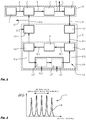
- FIG. 1 A schematic view of an optoelectronic oscillator is shown in Fig. 1 .
- a light source 1 which is selected as a laser, for instance, generates a signal carrier 2 of an optoelectronic oscillator to be transferred via optical delay line.
- Said signal carrier 2 is transferred from the light source 1 into a modulator 3 the task thereof is to modulate the carrier 2 with the oscillator signal.
- An optical signal 4 which in essence represents said carrier 2 modulated by the oscillator signal is further transferred as a signal 6 of the optoelectronic oscillator via delay means 5 to a photo detector 7.
- Said delay means 5 is selected for example as an optical fibre having the respective length, an optical resonator and similar.
- said carrier 2 is removed from the signal 6 of the optoelectronic oscillator and, as a result, only an oscillator signal 8 is present at the output from the photo detector 7. Afterwards, said oscillator signal 8 is led through a band-pass filter 9 back to said modulator 3.
- An oscillator loop is closed in this manner.
- an amplifier 10 optionally an adjustable amplifier, is provided between said photo detector 7 and said filter 9, whereas a phase shifter 11, preferably an adjustable phase shifter, is additionally provided between said filter 9 and said modulator 3.
- the amplifier 10 and the phase shifter 11 can be placed in an arbitrary order directly one after another, for example. Furthermore, the amplifier 10 is placed directly in succession to the photo detector 7, and followed by the phase shifter 11 and said filter 9, for instance.
- Said amplifier 10 can be either optical or electric amplifier, however, it can also be part of the modulator 3 and/or photo detector 7. In case the amplifier 10 is selected as the optical amplifier, it must be located in the optical section between the modulator and the photo detector. The optical path with the amplification could be implemented without the amplifier in the oscillator loop.
- the band-pass filter 9 can optionally be placed in the optical section O of the oscillator, however, the preferred embodiment refers to the filter 9 placed in the electric section E of the oscillator.
- Electric output I E may be arranged anywhere in the electric section E. In order to split signal of the oscillator to said output one can use a power divider, a directional coupler and similar. Optical output I O may be arranged anywhere in the optical section O between the modulator 3 and the photo detector 7. In order to split optical signal to said optical output I O one can use an optical directional coupler, for example.
- a feedback loop 12 is located in the electric section E of the optoelectronic oscillator and in parallel to the band-pass filter 9.
- Said feedback loop 12 comprises means 13 for coupling signal arranged between said amplifier 10 and directly in front of said filter 9, and means 14 for dividing signal, such as a splitter for instance, arranged directly after said filter 9 between the latter and said phase shifter 11.
- said means 13 for coupling signal is selected as combiner
- said means 14 for dividing signal is selected as splitter.
- means 15 for processing signal is located between said combiner 13 and said splitter 14.
- Said means 15 comprise at least an amplifier 15' and/or at least a phase shifter 15".
- Said oscillator signal 8 exiting said photo detector 7 is lead through said amplifier 10 and, afterwards, a processed signal 8.1 is fed through said combiner 13 as a combined signal 8.2 into said band-pass filter 9.
- a filtered signal 8.3 exiting said filter 9 is fed into said splitter 14 where it is split into two parts.
- a first part of the filtered signal 8.3 is returned via said phase shifter 11 as a wanted signal 8.6 to the modulator 3.
- a second par of the filtered signal 8.3 is fed as a feedback signal 8.4 into said means 15 for signal processing where from it is lead as a processed feedback signal 8.5 back to said combiner 13 where said feedback signal 8.5 is combined with the signal 8.1 coming from said amplifier 10.
- the signal originating in the filter 9 is resent through the same filter 9.
- the unit which is comprised of the band-pass filter 9 and said feedback loop 12 serves as a quality multiplier 16 of the band-pass filter 9.
- the optoelectronic oscillator comprising the feedback loop 12 and the quality multiplier 16, respectively, behaves as an ordinary optoelectronic oscillator comprising the band-pass filter 9 without the quality multiplier 16, which makes it possible to obtain very small bandwidth of the quality multiplier 16.
- the bandwidth of said quality multiplier 16 is determined by amplification of said feedback loop 12 of the filter 9, wherein said amplification of the feedback loop 12 must be set in a manner that the amplification of the entire loop of the quality multiplier 16 is less than "1". In case said amplification is greater than "1" the quality multiplier 16 starts to osculate.
- the bandwidth narrowness of the quality multiplier 16 depends on the control precision of the said amplification of said feedback loop 12 and, respectively, the loop of the quality multiplier 16. The closer to the value "1" lies the amplification of said loop the narrower is the quality multiplier 16. Thus, for instance, the bandwidth with the amplification of "0,9” is smaller than the bandwidth with the amplification of "0,8".
- the feedback loop 12 of the band-pass filter 9 has impact both on the bandwidth of the quality multiplier 16 and the insertion loss of the quality multiplier 16.
- the narrower the bandwidth of the quality multiplier 16 the lower the insertion loss of the quality multiplier 16.
- the insertion loss can grow above "1", resulting in the amplifier 10 in the loop of the optoelectronic oscillator to become entirely superfluous.
- the insertion loss and the bandwidth of the quality multiplier 16 also depend on operating of the rest of the optoelectronic loop. It is the key factor for the occurrence of the oscillation that the amplification of the entire loop of the optoelectronic oscillator comprises the exact value of "1" i.e. a so called Barkhausen amplitude criterion.
- the saturation power of the oscillator elements usually acts as a mechanism which limits the amplification. It is understood that the greater the signal power inside the oscillator the lesser is the amplification. Thus, the signal power increases as long as the amplification of the loop decreases to the value of precisely "1".
- the band-pass filter 9 comprising the feedback loop 12, or the quality multiplier 16 can be adjusted by itself and without any additional optoelectronic loop.
- the quality multiplier 16 can be set to a required bandwidth and to the central frequency by means of a circuit analyser. In theory, the quality multiplier 16 set in this manner could be inserted into the optoelectronic oscillator where it would retain its properties. However, this is not entirely true in the practice.
- connection impedances of the optoelectronic loop for the quality multiplier 16 are not equal to input and output impedances of the circuit analyser. The difference influences the operation of the feedback loop 12.
- the Barkhausen amplitude criterion and the relation between the amplification of the entire loop and the saturation power inside the feedback loop 12 is also to be taken into account. Due to said fact, the quality multiplier 16 and the optoelectronic oscillator must be tuned according to a method described in the continuation.
- the external control of the oscillator parameters must be enabled.
- Said parameters comprise the phase of the entire loop of the oscillator and the amplification of the feedback loop 12 of the filter 9.
- a means 15 for signal treatment is added to the optoelectronic oscillator at least in said feedback loop 12.
- said signal treatment means 15 is selected at least as an amplifier 15' and/or at least as a phase shifter 15".
- the presence of the phase shifter 11 in the oscillator loop is optional, since the phase can be varied in several ways. So for instance, the phase can be varied by varying the wavelength of the light, the bias of the modulator 3 and similar.
- the phase shifter 15" in the signal treatment means 15 arranged in the feedback loop 12 can be any arbitrary phase shifter which enables phase variations of the electric signal.
- the amplifier 15' which enables amplification variations in the feedback loop 12 is selected, for example, as an amplifier with adjustable amplification, or as an amplifier with a fixed amplification having additional adjustable attenuator.
- the method of tuning the optoelectronic oscillator having the quality multiplier 16 comprises the following steps.
- the first step comprises connecting the optoelectronic oscillator to a spectrum analyser. Said connection is possible directly via the electric output or indirectly via the optical output.
- the amplification of the feedback loop 12 is set in a manner that the amplification of the entire loop of the quality multiplier 16 is greater than "1". As a result, the quality multiplier 16 begins to oscillate.
- the previous step is followed by setting said spectrum analyser to the appropriate frequency range of the optoelectronic oscillator so that the oscillator signal can be observed on the spectrum analyser.
- the optical path is disconnected.
- the signal can still be observed on the spectrum analyser, however, the signal observed is now the signal of the oscillating filter 9 having the feedback loop 12, and, respectively, the quality multiplier 16.
- Said disconnection of the optical path can be carried out in the manner that a connection from the modulator 3 to the delay means 5, or from the delay means 5 to the photo detector 7 is disconnected.
- the optical path for instance, can be disconnected by removing an optical connector at the photo detector 7.
- the amplification of the feedback loop 12 is lowering until the quality multiplier 16 stops oscillating. At that point no signal can be detected by the spectrum analyser.
- the entire 2 ⁇ section of the phase shifter 15" in the feedback loop 12 is swept.
- the feedback loop 12 oscillates at the specific setting of the phase shifter 15" the entire 2 ⁇ section of the phase shifter in the loop of the optoelectronic oscillator is to be swept again. If the signal is absent, the method continues with the next step, otherwise the method returns to the step of lowering the amplification of the feedback loop 12.
- the optical path is re-connected again and the entire 2 ⁇ section of the phase shifter 15" in the feedback loop 12 is swept and, simultaneously, spectrum of the oscillator signal is recorded.
- the result of the recording is a comb-like frequency spectrum 17 with one or more frequency peaks 18 ( Fig. 2 ). If at least one of said frequency peaks 18 is not present, the step must be repeated in which the amplification of the loop of the quality multiplier 16 is set to the value above "1" in order for the quality multiplier 16 starts to oscillate. Every alteration of the phase shifter 15" in the feedback loop 12 changes frequency spectrum 17 of the signal of the oscillator.
- the result of the spectrum 17 recording is a sum of spectra with each value of the phase shifter 15", for example.
- the spectrum 17 can be recorded with a spectrum analyser.
- Said frequency spectrum 17 and, respectively, the available spectrum of the optoelectronic oscillator obtained by recording the oscillator spectrum during phase alteration in the feedback loop 12 is described in detail with the reference to Fig. 2 .
- the present embodiment shows the number of said frequency peaks 18 equal to five. The number of the frequency peaks 18 depends on how much larger than "1" is the oscillator's open loop amplification.
- the value U.1 of the phase shifter 11 in the main loop of the oscillator must be altered and repeated the step in which the entire 2 ⁇ section of the phase shifter 15" in the feedback loop 12 is swept and, simultaneously, spectrum of the oscillator signal is recorded.
- the phase shifter 11 shifts the available frequency spectrum 17. Only those frequency peaks 18 appear that overlap with the bandwidth of the band-pass filter 9 without the feedback loop 12. However, since one of the frequency peaks 18 in the available spectrum 17 is to be precisely in the centre of the bandwidth of the filter 9, the number of the peaks 18 must be odd.
- the value U.2 is used to set the frequency of the oscillator to the central peak 18 by means of the phase shifter 15" in the feedback loop 12. Setting the frequency to the central peak 18 is carried out in a manner that the value U.2 of the phase shifter 15" in the feedback loop 12 is varied and the signal spectrum 17 is compared with the recorded image obtained in the step in which the entire 2 ⁇ section of the phase shifter 15" in the feedback loop 12 is swept and, simultaneously, spectrum of the oscillator signal is recorded. The tuning is ended when the signal spectrum 17 is located in the central peak 18 of the recording.
Landscapes
- Stabilization Of Oscillater, Synchronisation, Frequency Synthesizers (AREA)
Description
- The present invention refers to a device for optoelectronic oscillator side-mode suppression, comprising an optical section, an electric section, and a band-pass filter with a feedback loop.
- Optoelectronic oscillators have been disclosed in
US 2005/057791 A1 ,DE 38 23 008 A1 ,US 7 697 579 B1 andEP 2 890 004 A1 - It is the object of the present invention to create an optoelectronic oscillator comprising a band-pass filter with a feedback loop according to
claim 1 and a method of tuning this device according toclaim 2. - The invention will be more readily understood on reading the following description of a nonlimiting embodiment and with reference to the accompanying drawings where
-
Fig. 1 shows a schematic view of an optoelectronic oscillator comprising a band-pass filter with a feedback loop according to the invention, -
Fig. 2 shows an available spectrum of the optoelectronic oscillator. - A schematic view of an optoelectronic oscillator is shown in
Fig. 1 . Alight source 1 which is selected as a laser, for instance, generates asignal carrier 2 of an optoelectronic oscillator to be transferred via optical delay line. Saidsignal carrier 2 is transferred from thelight source 1 into amodulator 3 the task thereof is to modulate thecarrier 2 with the oscillator signal. When direct laser modulation is utilized, than it is possible for themodulator 3 to constitute a part of thelight source 1. Anoptical signal 4 which in essence represents saidcarrier 2 modulated by the oscillator signal is further transferred as asignal 6 of the optoelectronic oscillator via delay means 5 to aphoto detector 7. Said delay means 5 is selected for example as an optical fibre having the respective length, an optical resonator and similar. By means of thephoto detector 7 saidcarrier 2 is removed from thesignal 6 of the optoelectronic oscillator and, as a result, only anoscillator signal 8 is present at the output from thephoto detector 7. Afterwards, saidoscillator signal 8 is led through a band-pass filter 9 back to saidmodulator 3. An oscillator loop is closed in this manner. In addition, anamplifier 10, optionally an adjustable amplifier, is provided between saidphoto detector 7 and saidfilter 9, whereas aphase shifter 11, preferably an adjustable phase shifter, is additionally provided between saidfilter 9 and saidmodulator 3. - Obviously, according to the present invention it is possible to provide another arrangement of the
amplifier 10 and thephase shifter 11. Theamplifier 10 and thephase shifter 11 can be placed in an arbitrary order directly one after another, for example. Furthermore, theamplifier 10 is placed directly in succession to thephoto detector 7, and followed by thephase shifter 11 and saidfilter 9, for instance. - Said
amplifier 10 can be either optical or electric amplifier, however, it can also be part of themodulator 3 and/orphoto detector 7. In case theamplifier 10 is selected as the optical amplifier, it must be located in the optical section between the modulator and the photo detector. The optical path with the amplification could be implemented without the amplifier in the oscillator loop. The band-pass filter 9 can optionally be placed in the optical section O of the oscillator, however, the preferred embodiment refers to thefilter 9 placed in the electric section E of the oscillator. - Electric output IE may be arranged anywhere in the electric section E. In order to split signal of the oscillator to said output one can use a power divider, a directional coupler and similar. Optical output IO may be arranged anywhere in the optical section O between the
modulator 3 and thephoto detector 7. In order to split optical signal to said optical output IO one can use an optical directional coupler, for example. - It is provided for according to the present invention, that a
feedback loop 12 is located in the electric section E of the optoelectronic oscillator and in parallel to the band-pass filter 9. Saidfeedback loop 12 comprises means 13 for coupling signal arranged between saidamplifier 10 and directly in front of saidfilter 9, and means 14 for dividing signal, such as a splitter for instance, arranged directly after saidfilter 9 between the latter and saidphase shifter 11. Here, it is provided that said means 13 for coupling signal is selected as combiner, and said means 14 for dividing signal is selected as splitter. Furthermore, according to the present invention is provided that means 15 for processing signal is located between saidcombiner 13 and saidsplitter 14. Said means 15 comprise at least an amplifier 15' and/or at least aphase shifter 15". Saidoscillator signal 8 exiting saidphoto detector 7 is lead through saidamplifier 10 and, afterwards, a processed signal 8.1 is fed through said combiner 13 as a combined signal 8.2 into said band-pass filter 9. A filtered signal 8.3 exiting saidfilter 9 is fed into saidsplitter 14 where it is split into two parts. A first part of the filtered signal 8.3 is returned via saidphase shifter 11 as a wanted signal 8.6 to themodulator 3. A second par of the filtered signal 8.3 is fed as a feedback signal 8.4 into saidmeans 15 for signal processing where from it is lead as a processed feedback signal 8.5 back to said combiner 13 where said feedback signal 8.5 is combined with the signal 8.1 coming from saidamplifier 10. With another words, the signal originating in thefilter 9 is resent through thesame filter 9. The unit which is comprised of the band-pass filter 9 and saidfeedback loop 12 serves as aquality multiplier 16 of the band-pass filter 9. - It is not allowed for the closed loop created by the
filter 9 and saidfeedback loop 12 to oscillate by itself. In fact, saidquality multiplier 16 and, respectively, saidfeedback loop 12 added to thefilter 9 form a positive feedback loop, however, the amplification of the entire loop is smaller than "1". Consequently, oscillation is disabled. In spite of that, phase noise of such an optoelectronic oscillator increases, however, for a smaller degree as if the amplification of the entire loop of thequality multiplier 16 would be grater that "1". - If the path travelled by the signal from the output of the
filter 9 via saidfeedback loop 12 to the input of thefilter 9 complies with required phase and power, respectively, additional phase treatment of the signal is not necessary. With saidfeedback loop 12, means 15 for signal processing is superfluous, if the signal 8.5 also complies with required phase and power, respectively. - When set properly, the optoelectronic oscillator comprising the
feedback loop 12 and thequality multiplier 16, respectively, behaves as an ordinary optoelectronic oscillator comprising the band-pass filter 9 without thequality multiplier 16, which makes it possible to obtain very small bandwidth of thequality multiplier 16. The bandwidth of saidquality multiplier 16 is determined by amplification of saidfeedback loop 12 of thefilter 9, wherein said amplification of thefeedback loop 12 must be set in a manner that the amplification of the entire loop of thequality multiplier 16 is less than "1". In case said amplification is greater than "1" thequality multiplier 16 starts to osculate. The bandwidth narrowness of thequality multiplier 16 depends on the control precision of the said amplification of saidfeedback loop 12 and, respectively, the loop of thequality multiplier 16. The closer to the value "1" lies the amplification of said loop the narrower is thequality multiplier 16. Thus, for instance, the bandwidth with the amplification of "0,9" is smaller than the bandwidth with the amplification of "0,8". - The
feedback loop 12 of the band-pass filter 9 has impact both on the bandwidth of thequality multiplier 16 and the insertion loss of thequality multiplier 16. The narrower the bandwidth of the quality multiplier 16 the lower the insertion loss of thequality multiplier 16. The insertion loss can grow above "1", resulting in theamplifier 10 in the loop of the optoelectronic oscillator to become entirely superfluous. - Besides on the conditions in said feedback loop of the
filter 9 and, respectively, on the settings of thefeedback loop 12 the insertion loss and the bandwidth of thequality multiplier 16 also depend on operating of the rest of the optoelectronic loop. It is the key factor for the occurrence of the oscillation that the amplification of the entire loop of the optoelectronic oscillator comprises the exact value of "1" i.e. a so called Barkhausen amplitude criterion. The saturation power of the oscillator elements usually acts as a mechanism which limits the amplification. It is understood that the greater the signal power inside the oscillator the lesser is the amplification. Thus, the signal power increases as long as the amplification of the loop decreases to the value of precisely "1". - In principle, the band-
pass filter 9 comprising thefeedback loop 12, or thequality multiplier 16 can be adjusted by itself and without any additional optoelectronic loop. Thequality multiplier 16 can be set to a required bandwidth and to the central frequency by means of a circuit analyser. In theory, the quality multiplier 16 set in this manner could be inserted into the optoelectronic oscillator where it would retain its properties. However, this is not entirely true in the practice. - Namely, connection impedances of the optoelectronic loop for the
quality multiplier 16 are not equal to input and output impedances of the circuit analyser. The difference influences the operation of thefeedback loop 12. In addition, the Barkhausen amplitude criterion and the relation between the amplification of the entire loop and the saturation power inside thefeedback loop 12 is also to be taken into account. Due to said fact, thequality multiplier 16 and the optoelectronic oscillator must be tuned according to a method described in the continuation. - In order to carry out the tuning method the external control of the oscillator parameters must be enabled. Said parameters comprise the phase of the entire loop of the oscillator and the amplification of the
feedback loop 12 of thefilter 9. For this reason, ameans 15 for signal treatment is added to the optoelectronic oscillator at least in saidfeedback loop 12. As already mentioned above, said signal treatment means 15 is selected at least as an amplifier 15' and/or at least as aphase shifter 15". The presence of thephase shifter 11 in the oscillator loop is optional, since the phase can be varied in several ways. So for instance, the phase can be varied by varying the wavelength of the light, the bias of themodulator 3 and similar. Thephase shifter 15" in the signal treatment means 15 arranged in thefeedback loop 12 can be any arbitrary phase shifter which enables phase variations of the electric signal. The amplifier 15' which enables amplification variations in thefeedback loop 12 is selected, for example, as an amplifier with adjustable amplification, or as an amplifier with a fixed amplification having additional adjustable attenuator. - The method of tuning the optoelectronic oscillator having the
quality multiplier 16 comprises the following steps. - The first step comprises connecting the optoelectronic oscillator to a spectrum analyser. Said connection is possible directly via the electric output or indirectly via the optical output.
- Afterwards, the amplification of the
feedback loop 12 is set in a manner that the amplification of the entire loop of thequality multiplier 16 is greater than "1". As a result, thequality multiplier 16 begins to oscillate. - The previous step is followed by setting said spectrum analyser to the appropriate frequency range of the optoelectronic oscillator so that the oscillator signal can be observed on the spectrum analyser. Than, the optical path is disconnected. The signal can still be observed on the spectrum analyser, however, the signal observed is now the signal of the
oscillating filter 9 having thefeedback loop 12, and, respectively, thequality multiplier 16. Said disconnection of the optical path can be carried out in the manner that a connection from themodulator 3 to the delay means 5, or from the delay means 5 to thephoto detector 7 is disconnected. The optical path, for instance, can be disconnected by removing an optical connector at thephoto detector 7. The amplification of thefeedback loop 12 is lowering until thequality multiplier 16 stops oscillating. At that point no signal can be detected by the spectrum analyser. - Further, the entire 2π section of the
phase shifter 15" in thefeedback loop 12 is swept. In case thefeedback loop 12 oscillates at the specific setting of thephase shifter 15" the entire 2π section of the phase shifter in the loop of the optoelectronic oscillator is to be swept again. If the signal is absent, the method continues with the next step, otherwise the method returns to the step of lowering the amplification of thefeedback loop 12. - Afterwards, the optical path is re-connected again and the entire 2π section of the
phase shifter 15" in thefeedback loop 12 is swept and, simultaneously, spectrum of the oscillator signal is recorded. The result of the recording is a comb-like frequency spectrum 17 with one or more frequency peaks 18 (Fig. 2 ). If at least one of said frequency peaks 18 is not present, the step must be repeated in which the amplification of the loop of thequality multiplier 16 is set to the value above "1" in order for thequality multiplier 16 starts to oscillate. Every alteration of thephase shifter 15" in thefeedback loop 12changes frequency spectrum 17 of the signal of the oscillator. The result of thespectrum 17 recording is a sum of spectra with each value of thephase shifter 15", for example. Thespectrum 17 can be recorded with a spectrum analyser. - Said
frequency spectrum 17 and, respectively, the available spectrum of the optoelectronic oscillator obtained by recording the oscillator spectrum during phase alteration in thefeedback loop 12 is described in detail with the reference toFig. 2 . The present embodiment shows the number of said frequency peaks 18 equal to five. The number of the frequency peaks 18 depends on how much larger than "1" is the oscillator's open loop amplification. - If the number of the frequency peaks 18 is even, the value U.1 of the
phase shifter 11 in the main loop of the oscillator must be altered and repeated the step in which the entire 2π section of thephase shifter 15" in thefeedback loop 12 is swept and, simultaneously, spectrum of the oscillator signal is recorded. Thephase shifter 11 shifts theavailable frequency spectrum 17. Only those frequency peaks 18 appear that overlap with the bandwidth of the band-pass filter 9 without thefeedback loop 12. However, since one of the frequency peaks 18 in theavailable spectrum 17 is to be precisely in the centre of the bandwidth of thefilter 9, the number of thepeaks 18 must be odd. - If the number of the frequency peaks 18 is odd, the value U.2 is used to set the frequency of the oscillator to the
central peak 18 by means of thephase shifter 15" in thefeedback loop 12. Setting the frequency to thecentral peak 18 is carried out in a manner that the value U.2 of thephase shifter 15" in thefeedback loop 12 is varied and thesignal spectrum 17 is compared with the recorded image obtained in the step in which the entire 2π section of thephase shifter 15" in thefeedback loop 12 is swept and, simultaneously, spectrum of the oscillator signal is recorded. The tuning is ended when thesignal spectrum 17 is located in thecentral peak 18 of the recording.
Claims (2)
- Optoelectronic oscillator configured for side-mode suppression, comprising an optical section (O), an electric section (E),
wherein the optoelectronic oscillator is made up of a closed loop comprising the optical (O) and the electrical section (E),
wherein the optical section comprises a modulated light source (1, 3) or a light source (1) followed by a modulator (3), optical delay means (5), and a photo detector (6),
wherein the electrical section (E) comprises a main loop including a bandpass filter (9), an amplifier (10), a first adjustable phase shifter (11) and a feedback-loop (12),
characterized in that
said feedback loop (12) comprises means (13) for signal coupling arranged directly in front of said band-pass filter (9), means (14) for signal splitting arranged directly after said band-pass filter (9), and means (15) for signal processing provided between said means (13) for signal coupling and means (14) for signal splitting,
wherein said means (15) for signal processing comprise an adjustable amplifier (15') and a second adjustable phase shifter (15") and said feedback loop (12) is
connected in parallel to the band-pass filter (9) in the electric section (E) and wherein the amplification of a loop provided by the filter (9) and the feedback loop (12) is less than "1", and wherein a unit comprising the band-pass filter (9) and said feedback loop (12) forms a quality multiplier (16) of the band-pass filter (9). - A method of tuning the optoelectronic oscillator according to claim 1, wherein the method comprises the following steps:a) connecting the optoelectronic oscillator to a spectrum analyser via an electric
output anywhere in the electric section;b) setting the amplification in said feedback loop (12) to a value greater than "1" in order for said said quality multiplier (16) to begin to oscillate;c) setting the spectrum analyser in order to observe the signal of the oscillator;d) disconnecting a connection from the modulator (3) to the delay means (5), or from the delay means (5) to the photo detector (7) in the optical section (O) in order to observe in the spectrum analyser a signal from said quality multiplier (16);e) lowering the amplification of said feedback loop (12) in order for said quality multiplier (16) to stop oscillating;f) sweeping the entire 2π section of said second adjustable phase shifter (15") in said feedback
loop (12);g) returning to step e) if said quality multiplier (16) oscillates at a specific setting of said second adjustable phase shifter (15") in said feedback loop (12);h) re-connecting the optical section (O);i) sweeping the entire 2π section of said phase shifter (15") in said feedback loop (12) and, simultaneously, recording said frequency spectrum (17) of the oscillator signal;j) returning to step b) if the frequency spectrum which is a result of said recording does not comprise at least one frequency peak;k) altering a value (U.1) of said first adjustable phase shifter (11) in the main loop of the oscillator, if the number of said frequency peaks is even, and repeating the step i);l) setting the frequency of the oscillator to a central frequency peak by means of said second adjustable phase shifter (15") in said feedback loop (12), if the number of said frequency peaks is odd.
Applications Claiming Priority (1)
| Application Number | Priority Date | Filing Date | Title |
|---|---|---|---|
| SI201500287A SI25111A (en) | 2015-12-02 | 2015-12-02 | Device for suppresion of side-mode oscillations of an optoelectronic oscillator |
Publications (2)
| Publication Number | Publication Date |
|---|---|
| EP3176944A1 EP3176944A1 (en) | 2017-06-07 |
| EP3176944B1 true EP3176944B1 (en) | 2021-06-16 |
Family
ID=57758386
Family Applications (1)
| Application Number | Title | Priority Date | Filing Date |
|---|---|---|---|
| EP16201017.7A Active EP3176944B1 (en) | 2015-12-02 | 2016-11-29 | Device for optoelectronic oscillator side-mode suppression |
Country Status (2)
| Country | Link |
|---|---|
| EP (1) | EP3176944B1 (en) |
| SI (1) | SI25111A (en) |
Families Citing this family (1)
| Publication number | Priority date | Publication date | Assignee | Title |
|---|---|---|---|---|
| CN118936530B (en) * | 2024-07-26 | 2025-12-09 | 北京邮电大学 | Optical fiber sensing method and system for photoelectric hybrid oscillation |
Family Cites Families (4)
| Publication number | Priority date | Publication date | Assignee | Title |
|---|---|---|---|---|
| DE3823008A1 (en) * | 1988-07-07 | 1990-01-11 | Telefunken Electronic Gmbh | SWITCHABLE OSCILLATOR |
| US7027675B2 (en) * | 2003-09-16 | 2006-04-11 | Hrl Laboratories, Llc | Frequency tuning of photonic oscillator using amplifier bias voltage |
| US7697579B1 (en) * | 2007-02-09 | 2010-04-13 | University Of Central Florida Research Foundation, Inc. | Optical frequency self stabilization in a coupled optoelectronic oscillator |
| SI24613A (en) * | 2013-12-30 | 2015-07-31 | Center Odliäśnosti Za Biosenzoriko, Instrumentacijo In Procesno Kontrolo | Method for the improvement of side-mode suppresion oscillations of an optoelectronic oscillator |
-
2015
- 2015-12-02 SI SI201500287A patent/SI25111A/en not_active IP Right Cessation
-
2016
- 2016-11-29 EP EP16201017.7A patent/EP3176944B1/en active Active
Also Published As
| Publication number | Publication date |
|---|---|
| EP3176944A1 (en) | 2017-06-07 |
| SI25111A (en) | 2017-06-30 |
Similar Documents
| Publication | Publication Date | Title |
|---|---|---|
| KR100600935B1 (en) | Wavelength lock loop servo control circuit and method of mutual alignment of the center wavelength of the electromagnetic signal and the center wavelength of the wavelength selection device | |
| CN107565305B (en) | Broadband Tunable Optoelectronic Oscillator Based on Cascaded Microwave Photonic Filters | |
| US11424594B2 (en) | Tunable optical pair source and related systems and methods | |
| CN106848827A (en) | A kind of laser locking method based on resonator | |
| US10084542B2 (en) | Microwave photonic notch filter | |
| CN115000806A (en) | Tunable ultra-narrow linewidth laser system based on optical frequency comb | |
| US20030002138A1 (en) | Gain stabilized raman effect optical amplifiers for coarse and dense wavelength multiplexers | |
| US6933485B2 (en) | Stabilizing power and wavelength of output radiation from a stabilized radiation source in optical communications systems | |
| JP3697350B2 (en) | Optical transmitter | |
| US10270536B2 (en) | Phase-sensitive regeneration without a phase-locked loop using brillouin amplification | |
| JP4807514B2 (en) | Optical clock extraction apparatus and method | |
| CN100423478C (en) | Method and apparatus for detection and compensation of polarization mode dispersion | |
| EP3176944A1 (en) | Device for optoelectronic oscillator side-mode suppression | |
| JP5230719B2 (en) | Apparatus and method for generating millimeter wave optical signal for use in optical data transmission | |
| CN104158069B (en) | A kind of optical-electronic oscillator based on three optical fiber ring structures | |
| WO2020073766A1 (en) | Multi-wavelength laser | |
| CN103457674A (en) | Infinite impulse response microwave photon filter and filtering method | |
| CN210326461U (en) | Low-phase noise photoelectric oscillator | |
| JP2011170253A (en) | Photoelectric oscillator | |
| CN113540932A (en) | Frequency sweep wideband signal generation system and sweep frequency wideband signal generation method | |
| CN113984677A (en) | Squeezed state detection method and device based on microcavity optical soliton extraction of coherent local oscillator light | |
| KR100776792B1 (en) | Optical clock signal extraction method and apparatus | |
| JP3831393B2 (en) | Optical transmitter | |
| CN107534505B (en) | A multi-carrier laser and method for generating multi-carrier light | |
| JP6202442B2 (en) | High-precision optical frequency stabilization method and high-precision optical frequency stabilization device |
Legal Events
| Date | Code | Title | Description |
|---|---|---|---|
| AK | Designated contracting states |
Kind code of ref document: A1 Designated state(s): AL AT BE BG CH CY CZ DE DK EE ES FI FR GB GR HR HU IE IS IT LI LT LU LV MC MK MT NL NO PL PT RO RS SE SI SK SM TR |
|
| AX | Request for extension of the european patent |
Extension state: BA ME |
|
| PUAI | Public reference made under article 153(3) epc to a published international application that has entered the european phase |
Free format text: ORIGINAL CODE: 0009012 |
|
| STAA | Information on the status of an ep patent application or granted ep patent |
Free format text: STATUS: THE APPLICATION HAS BEEN PUBLISHED |
|
| STAA | Information on the status of an ep patent application or granted ep patent |
Free format text: STATUS: REQUEST FOR EXAMINATION WAS MADE |
|
| 17P | Request for examination filed |
Effective date: 20171207 |
|
| RBV | Designated contracting states (corrected) |
Designated state(s): AL AT BE BG CH CY CZ DE DK EE ES FI FR GB GR HR HU IE IS IT LI LT LU LV MC MK MT NL NO PL PT RO RS SE SI SK SM TR |
|
| STAA | Information on the status of an ep patent application or granted ep patent |
Free format text: STATUS: EXAMINATION IS IN PROGRESS |
|
| 17Q | First examination report despatched |
Effective date: 20201209 |
|
| GRAP | Despatch of communication of intention to grant a patent |
Free format text: ORIGINAL CODE: EPIDOSNIGR1 |
|
| STAA | Information on the status of an ep patent application or granted ep patent |
Free format text: STATUS: GRANT OF PATENT IS INTENDED |
|
| INTG | Intention to grant announced |
Effective date: 20210319 |
|
| RIN1 | Information on inventor provided before grant (corrected) |
Inventor name: BOGATAJ, LUKA Inventor name: BATAGELJ, BOSTJAN Inventor name: VIDMAR, MATJAZ |
|
| GRAS | Grant fee paid |
Free format text: ORIGINAL CODE: EPIDOSNIGR3 |
|
| GRAA | (expected) grant |
Free format text: ORIGINAL CODE: 0009210 |
|
| STAA | Information on the status of an ep patent application or granted ep patent |
Free format text: STATUS: THE PATENT HAS BEEN GRANTED |
|
| AK | Designated contracting states |
Kind code of ref document: B1 Designated state(s): AL AT BE BG CH CY CZ DE DK EE ES FI FR GB GR HR HU IE IS IT LI LT LU LV MC MK MT NL NO PL PT RO RS SE SI SK SM TR |
|
| REG | Reference to a national code |
Ref country code: GB Ref legal event code: FG4D |
|
| REG | Reference to a national code |
Ref country code: CH Ref legal event code: EP |
|
| REG | Reference to a national code |
Ref country code: DE Ref legal event code: R096 Ref document number: 602016059320 Country of ref document: DE |
|
| REG | Reference to a national code |
Ref country code: AT Ref legal event code: REF Ref document number: 1403179 Country of ref document: AT Kind code of ref document: T Effective date: 20210715 |
|
| REG | Reference to a national code |
Ref country code: IE Ref legal event code: FG4D |
|
| REG | Reference to a national code |
Ref country code: LT Ref legal event code: MG9D |
|
| PG25 | Lapsed in a contracting state [announced via postgrant information from national office to epo] |
Ref country code: FI Free format text: LAPSE BECAUSE OF FAILURE TO SUBMIT A TRANSLATION OF THE DESCRIPTION OR TO PAY THE FEE WITHIN THE PRESCRIBED TIME-LIMIT Effective date: 20210616 Ref country code: LT Free format text: LAPSE BECAUSE OF FAILURE TO SUBMIT A TRANSLATION OF THE DESCRIPTION OR TO PAY THE FEE WITHIN THE PRESCRIBED TIME-LIMIT Effective date: 20210616 Ref country code: HR Free format text: LAPSE BECAUSE OF FAILURE TO SUBMIT A TRANSLATION OF THE DESCRIPTION OR TO PAY THE FEE WITHIN THE PRESCRIBED TIME-LIMIT Effective date: 20210616 Ref country code: BG Free format text: LAPSE BECAUSE OF FAILURE TO SUBMIT A TRANSLATION OF THE DESCRIPTION OR TO PAY THE FEE WITHIN THE PRESCRIBED TIME-LIMIT Effective date: 20210916 |
|
| REG | Reference to a national code |
Ref country code: AT Ref legal event code: MK05 Ref document number: 1403179 Country of ref document: AT Kind code of ref document: T Effective date: 20210616 |
|
| REG | Reference to a national code |
Ref country code: NL Ref legal event code: MP Effective date: 20210616 |
|
| PG25 | Lapsed in a contracting state [announced via postgrant information from national office to epo] |
Ref country code: GR Free format text: LAPSE BECAUSE OF FAILURE TO SUBMIT A TRANSLATION OF THE DESCRIPTION OR TO PAY THE FEE WITHIN THE PRESCRIBED TIME-LIMIT Effective date: 20210917 Ref country code: LV Free format text: LAPSE BECAUSE OF FAILURE TO SUBMIT A TRANSLATION OF THE DESCRIPTION OR TO PAY THE FEE WITHIN THE PRESCRIBED TIME-LIMIT Effective date: 20210616 Ref country code: RS Free format text: LAPSE BECAUSE OF FAILURE TO SUBMIT A TRANSLATION OF THE DESCRIPTION OR TO PAY THE FEE WITHIN THE PRESCRIBED TIME-LIMIT Effective date: 20210616 Ref country code: SE Free format text: LAPSE BECAUSE OF FAILURE TO SUBMIT A TRANSLATION OF THE DESCRIPTION OR TO PAY THE FEE WITHIN THE PRESCRIBED TIME-LIMIT Effective date: 20210616 Ref country code: NO Free format text: LAPSE BECAUSE OF FAILURE TO SUBMIT A TRANSLATION OF THE DESCRIPTION OR TO PAY THE FEE WITHIN THE PRESCRIBED TIME-LIMIT Effective date: 20210916 |
|
| PG25 | Lapsed in a contracting state [announced via postgrant information from national office to epo] |
Ref country code: SM Free format text: LAPSE BECAUSE OF FAILURE TO SUBMIT A TRANSLATION OF THE DESCRIPTION OR TO PAY THE FEE WITHIN THE PRESCRIBED TIME-LIMIT Effective date: 20210616 Ref country code: SK Free format text: LAPSE BECAUSE OF FAILURE TO SUBMIT A TRANSLATION OF THE DESCRIPTION OR TO PAY THE FEE WITHIN THE PRESCRIBED TIME-LIMIT Effective date: 20210616 Ref country code: CZ Free format text: LAPSE BECAUSE OF FAILURE TO SUBMIT A TRANSLATION OF THE DESCRIPTION OR TO PAY THE FEE WITHIN THE PRESCRIBED TIME-LIMIT Effective date: 20210616 Ref country code: EE Free format text: LAPSE BECAUSE OF FAILURE TO SUBMIT A TRANSLATION OF THE DESCRIPTION OR TO PAY THE FEE WITHIN THE PRESCRIBED TIME-LIMIT Effective date: 20210616 Ref country code: AT Free format text: LAPSE BECAUSE OF FAILURE TO SUBMIT A TRANSLATION OF THE DESCRIPTION OR TO PAY THE FEE WITHIN THE PRESCRIBED TIME-LIMIT Effective date: 20210616 Ref country code: NL Free format text: LAPSE BECAUSE OF FAILURE TO SUBMIT A TRANSLATION OF THE DESCRIPTION OR TO PAY THE FEE WITHIN THE PRESCRIBED TIME-LIMIT Effective date: 20210616 Ref country code: RO Free format text: LAPSE BECAUSE OF FAILURE TO SUBMIT A TRANSLATION OF THE DESCRIPTION OR TO PAY THE FEE WITHIN THE PRESCRIBED TIME-LIMIT Effective date: 20210616 Ref country code: PT Free format text: LAPSE BECAUSE OF FAILURE TO SUBMIT A TRANSLATION OF THE DESCRIPTION OR TO PAY THE FEE WITHIN THE PRESCRIBED TIME-LIMIT Effective date: 20211018 Ref country code: ES Free format text: LAPSE BECAUSE OF FAILURE TO SUBMIT A TRANSLATION OF THE DESCRIPTION OR TO PAY THE FEE WITHIN THE PRESCRIBED TIME-LIMIT Effective date: 20210616 |
|
| PG25 | Lapsed in a contracting state [announced via postgrant information from national office to epo] |
Ref country code: PL Free format text: LAPSE BECAUSE OF FAILURE TO SUBMIT A TRANSLATION OF THE DESCRIPTION OR TO PAY THE FEE WITHIN THE PRESCRIBED TIME-LIMIT Effective date: 20210616 |
|
| REG | Reference to a national code |
Ref country code: DE Ref legal event code: R097 Ref document number: 602016059320 Country of ref document: DE |
|
| PLBE | No opposition filed within time limit |
Free format text: ORIGINAL CODE: 0009261 |
|
| STAA | Information on the status of an ep patent application or granted ep patent |
Free format text: STATUS: NO OPPOSITION FILED WITHIN TIME LIMIT |
|
| PG25 | Lapsed in a contracting state [announced via postgrant information from national office to epo] |
Ref country code: DK Free format text: LAPSE BECAUSE OF FAILURE TO SUBMIT A TRANSLATION OF THE DESCRIPTION OR TO PAY THE FEE WITHIN THE PRESCRIBED TIME-LIMIT Effective date: 20210616 |
|
| 26N | No opposition filed |
Effective date: 20220317 |
|
| PG25 | Lapsed in a contracting state [announced via postgrant information from national office to epo] |
Ref country code: AL Free format text: LAPSE BECAUSE OF FAILURE TO SUBMIT A TRANSLATION OF THE DESCRIPTION OR TO PAY THE FEE WITHIN THE PRESCRIBED TIME-LIMIT Effective date: 20210616 |
|
| REG | Reference to a national code |
Ref country code: DE Ref legal event code: R119 Ref document number: 602016059320 Country of ref document: DE |
|
| PG25 | Lapsed in a contracting state [announced via postgrant information from national office to epo] |
Ref country code: MC Free format text: LAPSE BECAUSE OF FAILURE TO SUBMIT A TRANSLATION OF THE DESCRIPTION OR TO PAY THE FEE WITHIN THE PRESCRIBED TIME-LIMIT Effective date: 20210616 |
|
| REG | Reference to a national code |
Ref country code: CH Ref legal event code: PL |
|
| GBPC | Gb: european patent ceased through non-payment of renewal fee |
Effective date: 20211129 |
|
| PG25 | Lapsed in a contracting state [announced via postgrant information from national office to epo] |
Ref country code: LU Free format text: LAPSE BECAUSE OF NON-PAYMENT OF DUE FEES Effective date: 20211129 Ref country code: IT Free format text: LAPSE BECAUSE OF FAILURE TO SUBMIT A TRANSLATION OF THE DESCRIPTION OR TO PAY THE FEE WITHIN THE PRESCRIBED TIME-LIMIT Effective date: 20210616 Ref country code: BE Free format text: LAPSE BECAUSE OF NON-PAYMENT OF DUE FEES Effective date: 20211130 |
|
| REG | Reference to a national code |
Ref country code: BE Ref legal event code: MM Effective date: 20211130 |
|
| PG25 | Lapsed in a contracting state [announced via postgrant information from national office to epo] |
Ref country code: IE Free format text: LAPSE BECAUSE OF NON-PAYMENT OF DUE FEES Effective date: 20211129 Ref country code: GB Free format text: LAPSE BECAUSE OF NON-PAYMENT OF DUE FEES Effective date: 20211129 Ref country code: DE Free format text: LAPSE BECAUSE OF NON-PAYMENT OF DUE FEES Effective date: 20220601 |
|
| PG25 | Lapsed in a contracting state [announced via postgrant information from national office to epo] |
Ref country code: FR Free format text: LAPSE BECAUSE OF NON-PAYMENT OF DUE FEES Effective date: 20211130 |
|
| PG25 | Lapsed in a contracting state [announced via postgrant information from national office to epo] |
Ref country code: HU Free format text: LAPSE BECAUSE OF FAILURE TO SUBMIT A TRANSLATION OF THE DESCRIPTION OR TO PAY THE FEE WITHIN THE PRESCRIBED TIME-LIMIT; INVALID AB INITIO Effective date: 20161129 |
|
| PG25 | Lapsed in a contracting state [announced via postgrant information from national office to epo] |
Ref country code: CY Free format text: LAPSE BECAUSE OF FAILURE TO SUBMIT A TRANSLATION OF THE DESCRIPTION OR TO PAY THE FEE WITHIN THE PRESCRIBED TIME-LIMIT Effective date: 20210616 |
|
| PG25 | Lapsed in a contracting state [announced via postgrant information from national office to epo] |
Ref country code: LI Free format text: LAPSE BECAUSE OF NON-PAYMENT OF DUE FEES Effective date: 20220630 Ref country code: CH Free format text: LAPSE BECAUSE OF NON-PAYMENT OF DUE FEES Effective date: 20220630 |
|
| PG25 | Lapsed in a contracting state [announced via postgrant information from national office to epo] |
Ref country code: MK Free format text: LAPSE BECAUSE OF FAILURE TO SUBMIT A TRANSLATION OF THE DESCRIPTION OR TO PAY THE FEE WITHIN THE PRESCRIBED TIME-LIMIT Effective date: 20210616 |
|
| PG25 | Lapsed in a contracting state [announced via postgrant information from national office to epo] |
Ref country code: TR Free format text: LAPSE BECAUSE OF FAILURE TO SUBMIT A TRANSLATION OF THE DESCRIPTION OR TO PAY THE FEE WITHIN THE PRESCRIBED TIME-LIMIT Effective date: 20210616 |
|
| PG25 | Lapsed in a contracting state [announced via postgrant information from national office to epo] |
Ref country code: MT Free format text: LAPSE BECAUSE OF FAILURE TO SUBMIT A TRANSLATION OF THE DESCRIPTION OR TO PAY THE FEE WITHIN THE PRESCRIBED TIME-LIMIT Effective date: 20210616 |