EP3176734A1 - Rfic module and rfid tag equipped with same - Google Patents
Rfic module and rfid tag equipped with same Download PDFInfo
- Publication number
- EP3176734A1 EP3176734A1 EP15863302.4A EP15863302A EP3176734A1 EP 3176734 A1 EP3176734 A1 EP 3176734A1 EP 15863302 A EP15863302 A EP 15863302A EP 3176734 A1 EP3176734 A1 EP 3176734A1
- Authority
- EP
- European Patent Office
- Prior art keywords
- coil
- coil portion
- substrate
- terminal electrode
- disposed
- Prior art date
- Legal status (The legal status is an assumption and is not a legal conclusion. Google has not performed a legal analysis and makes no representation as to the accuracy of the status listed.)
- Granted
Links
Images







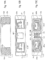


Classifications
-
- G—PHYSICS
- G06—COMPUTING OR CALCULATING; COUNTING
- G06K—GRAPHICAL DATA READING; PRESENTATION OF DATA; RECORD CARRIERS; HANDLING RECORD CARRIERS
- G06K19/00—Record carriers for use with machines and with at least a part designed to carry digital markings
- G06K19/06—Record carriers for use with machines and with at least a part designed to carry digital markings characterised by the kind of the digital marking, e.g. shape, nature, code
- G06K19/067—Record carriers with conductive marks, printed circuits or semiconductor circuit elements, e.g. credit or identity cards also with resonating or responding marks without active components
- G06K19/07—Record carriers with conductive marks, printed circuits or semiconductor circuit elements, e.g. credit or identity cards also with resonating or responding marks without active components with integrated circuit chips
- G06K19/077—Constructional details, e.g. mounting of circuits in the carrier
-
- G—PHYSICS
- G06—COMPUTING OR CALCULATING; COUNTING
- G06K—GRAPHICAL DATA READING; PRESENTATION OF DATA; RECORD CARRIERS; HANDLING RECORD CARRIERS
- G06K19/00—Record carriers for use with machines and with at least a part designed to carry digital markings
- G06K19/06—Record carriers for use with machines and with at least a part designed to carry digital markings characterised by the kind of the digital marking, e.g. shape, nature, code
- G06K19/067—Record carriers with conductive marks, printed circuits or semiconductor circuit elements, e.g. credit or identity cards also with resonating or responding marks without active components
- G06K19/07—Record carriers with conductive marks, printed circuits or semiconductor circuit elements, e.g. credit or identity cards also with resonating or responding marks without active components with integrated circuit chips
-
- G—PHYSICS
- G06—COMPUTING OR CALCULATING; COUNTING
- G06K—GRAPHICAL DATA READING; PRESENTATION OF DATA; RECORD CARRIERS; HANDLING RECORD CARRIERS
- G06K19/00—Record carriers for use with machines and with at least a part designed to carry digital markings
- G06K19/06—Record carriers for use with machines and with at least a part designed to carry digital markings characterised by the kind of the digital marking, e.g. shape, nature, code
- G06K19/067—Record carriers with conductive marks, printed circuits or semiconductor circuit elements, e.g. credit or identity cards also with resonating or responding marks without active components
- G06K19/07—Record carriers with conductive marks, printed circuits or semiconductor circuit elements, e.g. credit or identity cards also with resonating or responding marks without active components with integrated circuit chips
- G06K19/077—Constructional details, e.g. mounting of circuits in the carrier
- G06K19/07749—Constructional details, e.g. mounting of circuits in the carrier the record carrier being capable of non-contact communication, e.g. constructional details of the antenna of a non-contact smart card
- G06K19/07771—Constructional details, e.g. mounting of circuits in the carrier the record carrier being capable of non-contact communication, e.g. constructional details of the antenna of a non-contact smart card the record carrier comprising means for minimising adverse effects on the data communication capability of the record carrier, e.g. minimising Eddy currents induced in a proximate metal or otherwise electromagnetically interfering object
-
- G—PHYSICS
- G06—COMPUTING OR CALCULATING; COUNTING
- G06K—GRAPHICAL DATA READING; PRESENTATION OF DATA; RECORD CARRIERS; HANDLING RECORD CARRIERS
- G06K19/00—Record carriers for use with machines and with at least a part designed to carry digital markings
- G06K19/06—Record carriers for use with machines and with at least a part designed to carry digital markings characterised by the kind of the digital marking, e.g. shape, nature, code
- G06K19/067—Record carriers with conductive marks, printed circuits or semiconductor circuit elements, e.g. credit or identity cards also with resonating or responding marks without active components
- G06K19/07—Record carriers with conductive marks, printed circuits or semiconductor circuit elements, e.g. credit or identity cards also with resonating or responding marks without active components with integrated circuit chips
- G06K19/077—Constructional details, e.g. mounting of circuits in the carrier
- G06K19/07749—Constructional details, e.g. mounting of circuits in the carrier the record carrier being capable of non-contact communication, e.g. constructional details of the antenna of a non-contact smart card
- G06K19/07773—Antenna details
- G06K19/07786—Antenna details the antenna being of the HF type, such as a dipole
-
- H—ELECTRICITY
- H01—ELECTRIC ELEMENTS
- H01F—MAGNETS; INDUCTANCES; TRANSFORMERS; SELECTION OF MATERIALS FOR THEIR MAGNETIC PROPERTIES
- H01F17/00—Fixed inductances of the signal type
- H01F17/0006—Printed inductances
- H01F17/0013—Printed inductances with stacked layers
-
- H—ELECTRICITY
- H01—ELECTRIC ELEMENTS
- H01F—MAGNETS; INDUCTANCES; TRANSFORMERS; SELECTION OF MATERIALS FOR THEIR MAGNETIC PROPERTIES
- H01F27/00—Details of transformers or inductances, in general
- H01F27/28—Coils; Windings; Conductive connections
- H01F27/29—Terminals; Tapping arrangements for signal inductances
- H01F27/292—Surface mounted devices
-
- H—ELECTRICITY
- H01—ELECTRIC ELEMENTS
- H01Q—ANTENNAS, i.e. RADIO AERIALS
- H01Q1/00—Details of, or arrangements associated with, antennas
- H01Q1/12—Supports; Mounting means
- H01Q1/22—Supports; Mounting means by structural association with other equipment or articles
- H01Q1/2208—Supports; Mounting means by structural association with other equipment or articles associated with components used in interrogation type services, i.e. in systems for information exchange between an interrogator/reader and a tag/transponder, e.g. in Radio Frequency Identification [RFID] systems
- H01Q1/2225—Supports; Mounting means by structural association with other equipment or articles associated with components used in interrogation type services, i.e. in systems for information exchange between an interrogator/reader and a tag/transponder, e.g. in Radio Frequency Identification [RFID] systems used in active tags, i.e. provided with its own power source or in passive tags, i.e. deriving power from RF signal
-
- H—ELECTRICITY
- H01—ELECTRIC ELEMENTS
- H01Q—ANTENNAS, i.e. RADIO AERIALS
- H01Q1/00—Details of, or arrangements associated with, antennas
- H01Q1/40—Radiating elements coated with or embedded in protective material
-
- H—ELECTRICITY
- H01—ELECTRIC ELEMENTS
- H01Q—ANTENNAS, i.e. RADIO AERIALS
- H01Q7/00—Loop antennas with a substantially uniform current distribution around the loop and having a directional radiation pattern in a plane perpendicular to the plane of the loop
-
- H—ELECTRICITY
- H01—ELECTRIC ELEMENTS
- H01Q—ANTENNAS, i.e. RADIO AERIALS
- H01Q9/00—Electrically-short antennas having dimensions not more than twice the operating wavelength and consisting of conductive active radiating elements
- H01Q9/04—Resonant antennas
- H01Q9/16—Resonant antennas with feed intermediate between the extremities of the antenna, e.g. centre-fed dipole
- H01Q9/26—Resonant antennas with feed intermediate between the extremities of the antenna, e.g. centre-fed dipole with folded element or elements, the folded parts being spaced apart a small fraction of operating wavelength
-
- H—ELECTRICITY
- H01—ELECTRIC ELEMENTS
- H01F—MAGNETS; INDUCTANCES; TRANSFORMERS; SELECTION OF MATERIALS FOR THEIR MAGNETIC PROPERTIES
- H01F17/00—Fixed inductances of the signal type
- H01F17/0006—Printed inductances
- H01F2017/0073—Printed inductances with a special conductive pattern, e.g. flat spiral
Definitions
- the present invention relates to an RFIC (Radio Frequency Integrated Circuit) module and an RFID (Radio Frequency IDentifier) tag including the same and, more particularly, to an RFIC module and an RFID tag including an RFIC chip that includes two input/output terminals and a coil conductor that includes two coil ends respectively connected to the two input/output terminals.
- RFIC Radio Frequency Integrated Circuit
- RFID Radio Frequency IDentifier
- an RFID system For an article information management system, an RFID system has recently been used and the RFID system enables a reader/writer and an RFID tag applied to an article to communicate in a non-contact manner utilizing a magnetic field or an electromagnetic field so as to transmit predetermined information.
- This RFID tag includes an RFIC chip storing predetermined information and processing a predetermined radio signal and an antenna element (radiator) transmitting/receiving high-frequency signals and is affixed to various articles (or packing materials thereof) to be managed when used.
- the RFID system is typically an HF band RFID system using the 13.56 MHz band or a UHF band RFID system using the 900 MHz band. Particularly, because of a comparatively long communication distance and an ability to read multiple tags together, the UHF band RFID system is considered as a promising system for article management.
- a tag having a structure disclosed in Patent Document 1 ( WO 2010/146944 ) is known as the UHF band RFID tag.
- Patent Document 1 WO 2010/146944
- the RFID tag of Patent Document 1 includes two coil conductors adjacently arranged in a ceramic multilayer substrate and a stray capacitance is easily provided between the two coil conductors. If the coil conductors are coupled via the stray capacitance, a resonance circuit defined by a stray capacitance component and the inductance components of the coil conductors is provided, so that a passband width may be narrowed.
- An RFIC module is an RFIC module comprising an RFIC chip mounted on a substrate and including a first input/output terminal and a second input/output terminal; a power feeding circuit built into the substrate and including a coil conductor including a first coil end and a second coil end respectively connected to the first input/output terminal and the second input/output terminal; a first terminal electrode disposed on a principal surface of the substrate and connected to a first position of the coil conductor; and a second terminal electrode disposed on the principal surface of the substrate and connected to a second position of the coil conductor, the coil conductor including a first coil portion and a second coil portion, the first coil portion being disposed in a section extending from the first coil end to the first position, the first coil portion including a first winding axis extending in a direction intersecting with the principal surface of the substrate, the second coil portion being disposed in a section extending from the second coil end to the second position, the second coil portion including a second winding axi
- the RFIC chip defines and functions as a ground or a shield, so that the first coil portion and the second coil portion are not significantly magnetically or capacitively coupled to each other. This enables a reduction in the risk of narrowing the passband of communication signals.
- the RFIC chip is built into the substrate, and the power feeding circuit is disposed at a position overlapping with the RFIC chip when viewed in a direction perpendicular to a predetermined side surface of the substrate. This results to an increase in the shield effect due to the RFIC chip.
- the substrate is a flexible substrate with the principal surface having a rectangle, and the first coil portion and the second coil portion are respectively located on opposing end sides of the long sides drawing the rectangle.
- the first coil portion and the second coil portion are located at respective positions spaced away from the RFIC chip in a planar view of the substrate. This increases the shield effect due to the RFIC chip.
- the first coil portion and the second coil portion are connected and wound such that magnetic fields generated by the respective coil portions are in phase.
- the first coil portion and the second coil portion are not significantly coupled through the magnetic fields.
- the first terminal electrode dose not overlap with a center of a coil opening of the first coil portion and the second terminal electrode does not overlap with a center of a coil opening of the second coil portion.
- the magnetic field generated by the first coil portion and the second coil portion is not significantly disturbed by the first terminal electrode and the second terminal electrode.
- the coil conductor further includes a third coil portion and a fourth coil portion connected in series between the first position and the second position and respectively overlapping with the first coil portion and the second coil portion in a planar view of the substrate.
- the additional resonance produced by the parasitic capacitance between the first coil portion and the second coil portion is coupled to the resonance produced by the third coil portion and the fourth coil portion.
- broadband resonance frequency characteristics are achieved.
- the power feeding circuit further includes a first connection conductor extending in a thickness direction of the substrate at a position overlapping with the first terminal electrode in a planar view of the substrate to connect the first coil portion and the third coil portion in series and a second connection conductor extending in a thickness direction of the substrate at a position overlapping with the second terminal electrode in a planar view of the substrate to connect the second coil portion and the fourth coil portion in series.
- the first connection conductor and the second connection conductor are disposed in a rigid area of the substrate in the planar view. This prevents a reduction in the flexibility of the RFIC module.
- first coil portion, the second coil portion, the third coil portion, and the fourth coil portion are connected and wound such that magnetic fields generated by the coil conductor are in phase among the first coil portion, the second coil portion, the third coil portion, and the fourth coil portion. This increases the magnetic field strength.
- the third coil portion and the fourth coil portion are disposed on a layer adjacent to a layer on which the first and second terminal electrodes are provided, and the first coil portion and the second coil portion are disposed on a layer that is adjacent to the layer on which the third coil portion and the fourth coil portion are disposed on the side opposite to the layer on which the first and second terminal electrodes are provided.
- the first coil portion and the second coil portion are disposed at positions spaced further away from the first terminal electrode and the second terminal electrode as compared to the third coil portion and the fourth coil portion. Therefore, even if the inductance values of the first coil portion and the second coil portion are increased, the magnetic field generation by the first coil portion and the second coil portion is not significantly disturbed by the first terminal electrode and the second terminal electrode.
- the inductance values of the first coil portion and the second coil portion are larger than the inductance values of the third coil portion and the fourth coil portion, respectively.
- Such a structure increases the significance of disposing the first coil portion and the second coil portion at positions spaced away from the first terminal electrode and the second terminal electrode.
- An RFID tag is an RFID tag comprising an RFIC module; and an antenna element connected to the RFIC module, the RFIC module including an RFIC chip mounted on a substrate and including a first input/output terminal and a second input/output terminal, a power feeding circuit built into the substrate and including a coil conductor including a first coil end and a second coil end respectively connected to the first input/output terminal and the second input/output terminal, a first terminal electrode disposed on a principal surface of the substrate and connected to a first position of the coil conductor, and a second terminal electrode disposed on the principal surface of the substrate and connected to a second position of the coil conductor, the coil conductor including a first coil portion and a second coil portion, the first coil portion being disposed in a section extending from the first coil end to the first position, the first coil portion including a first winding axis extending in a direction intersecting with the principal surface of the substrate, the second coil portion being disposed in a section extending from the
- the RFIC chip defines and functions as a ground or a shield, so that the first coil portion and the second coil portion are not significantly magnetically or capacitively coupled to each other. This enables a reduction in the risk of narrowing the passband of communication signals.
- the antenna element is a dipole type antenna element including a first antenna portion connected at one end to the first terminal electrode and a second antenna portion connected at one end to the second terminal electrode.
- the RFID tag is able to be easily produced.
- the antenna element is a loop type antenna element including one end connected to the first terminal electrode and the other end connected to the second terminal electrode.
- the antenna characteristics are not significantly varied by the permittivity of an article to which the RFID tag is affixed.
- An RFIC module of the present invention is an RFIC module comprising an RFIC chip mounted on a substrate and including a first input/output terminal and a second input/output terminal; and a power feeding circuit built into the substrate and including a coil conductor including a first coil end and a second coil end respectively connected to the first input/output terminal and the second input/output terminal, the coil conductor including a first coil portion and a second coil portion connected in series and located at positions with the RFIC chip interposed therebetween in a planar view of the substrate, the first coil portion and the second coil portion respectively including a first winding axis and a second winding axis with the RFIC chip interposed therebetween in a planar view of the substrate, the first winding axis and the second winding axis extending in a direction intersecting with the principal surface.
- the RFIC chip defines and functions as a ground or a shield, so that the first coil portion and the second coil portion are not significantly magnetically or capacitively coupled to each other. This enables a reduction in the risk of narrowing the passband of communication signals.
- the first coil portion and the second coil portion define and function as an antenna element and, therefore, a small-sized RFID tag is achieved.
- the coil conductor further includes a third coil portion and a fourth coil portion connected in series between the first coil portion and the second coil portion and respectively overlapping with the first coil portion and the second coil portion in a planar view of the substrate.
- the additional resonance produced by the parasitic capacitance between the first coil portion and the second coil portion is coupled to the resonance produced by the third coil portion and the fourth coil portion.
- broadband resonance frequency characteristics are achieved.
- the risk of narrowing the passband of communication signals is able to be reduced by enabling the RFIC chip to define and function as a ground or a shield.
- an RFIC module 10 of this embodiment is an RFIC module typically corresponding to a communication frequency of the 900 MHz band, i.e., the UHF band, and includes a multilayer substrate 12 with a principal surface having a rectangle shape.
- the multilayer substrate 12 includes a base body that is a laminated body formed by laminating flexible resin insulation layers of polyimide, liquid crystal polymer, etc., and the multilayer substrate 12 itself exhibits flexibility.
- the insulation layers made of these materials include a permittivity smaller than that of ceramic base material layers made of LTCC.
- the X-axis extends a longitudinal direction of the multilayer substrate 12
- the Y-axis extends in a width direction of the multilayer substrate 12
- the Z-axis extends in a thickness direction of the multilayer substrate 12.
- an RFIC chip 16 and a power feeding circuit 18 are built into the multilayer substrate 12, and a first terminal electrode 14a and a second terminal electrode 14b are provided on one principal surface of the multilayer substrate 12.
- the RFIC chip 16 is an ultrathin package, includes a structure in which various elements are built into a hard semiconductor substrate made of a semiconductor such as silicon, and includes the one principal surface and the other principal surface drawing a square.
- a first input/output terminal 16a and a second input/output terminal 16b are provided on the other principal surface of the RFIC chip 16 (described in detail later).
- the RFIC chip 16 is located at the center in each of the X-, Y-, and Z-axis directions inside the multilayer substrate 12 in a configuration in which the sides of the square extend along the X-axis or the Y-axis and the one principal surface and the other principal surface face the positive side and the negative side, respectively, in the Z-axis direction.
- the power feeding circuit 18 includes a coil conductor 20 and interlayer connection conductors 24a and 24b (described in detail later).
- the coil conductor 20 includes coil patterns 20a to 20c.
- a first coil portion CIL1 defines a portion of the coil pattern 20a
- a second coil portion CIL2 defines a portion of the coil pattern 20b
- a third coil portion CIL3 and a fourth coil portion CIL4 define portions of the coil pattern 20c.
- the first coil portion CIL1, the third coil portion CIL3, and the interlayer connection conductor 24a are arranged in the Z-axis direction at positions on the negative side in the X-axis direction
- the second coil portion CIL2, the fourth coil portion CIL4, and the interlayer connection conductor 24b are arranged in the Z-axis direction at positions on the positive side in the X-axis direction.
- the RFIC chip 16 is located between the first coil portion CIL1 and the second coil portion CIL2 and between the third coil portion CIL3 and the fourth coil portion CIL4 when the multilayer substrate 12 is viewed in each of the Z- and Y-axis directions.
- the first terminal electrode 14a is disposed at a position on the negative side in the X-axis direction
- the second terminal electrode 14b is disposed at a position on the positive side in the X-axis direction.
- Both of the first terminal electrode 14a and the second terminal electrode 14b are provided of a flexible copper foil having a strip shape and include the respective principal surface sizes identical to each other.
- the short sides of the strip extend along the X-axis, and the long sides of the strip extend along the Y-axis.
- the RFIC chip 16 is interposed between a portion of the power feeding circuit 18 and another portion of the power feeding circuit 18.
- the RFIC chip 16 overlaps with the power feeding circuit 18.
- the power feeding circuit 18 partially overlaps with each of the first and second terminal electrodes 14a, 14b.
- each of the insulation layers of the laminated body is as thin as 10 ⁇ m or greater and 100 ⁇ m or less, the RFIC chip 16 and the power feeding circuit 18 built into the multilayer substrate 12 can be seen through on the outside. Therefore, the connection state (presence of a broken wire) of the RFIC chip 16 and the power feeding circuit 18 is able to be easily confirmed.
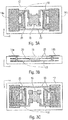
- the multilayer substrate 12 includes three laminated sheet-shaped insulation layers 12a to 12c. Among these layers, the insulation layer 12a is an upper layer, the insulation layer 12b is an intermediate layer, and the insulation layer 12c is a lower layer.
- the first terminal electrode 14a and the second terminal electrode 14b are provided on one principal surface of the insulation layer 12a. As described above, the first terminal electrode 14a is disposed on the negative side in the X-axis direction and the second terminal electrode 14b is disposed on the positive side in the X-axis direction.
- a rectangular through-hole HL1 is provided and extends to the other principal surface.
- the size of the through-hole HL1 is matched to the size of the RFIC chip 16.
- the coil pattern 20c made of a flexible copper foil and extends in a belt shape is provided around the through-hole HL1 on the one principal surface of the insulation layer 12b.
- One end of the coil pattern 20c is disposed at a position overlapping with the first terminal electrode 14a in the planar view and is connected to the first terminal electrode 14a by an interlayer connection conductor 22a extending in the Z-axis direction.
- the other end of the coil pattern 20c is disposed at a position overlapping with the second terminal electrode 14b in the planar view and is connected to the second terminal electrode 14b by an interlayer connection conductor 22b extending in the Z-axis direction.
- the interlayer connection conductors 22a, 22b, and the interlayer connection conductors 24a, 24b, described later are hard metal masses containing Sn as a main component.
- the coil pattern 20c winds around the one end twice in the counterclockwise direction, extends to near the end portion of the negative side in the Y-axis direction, and then extends into the positive side in the X-axis direction.
- the coil pattern 20c subsequently bends near the end portion of the positive side in the X-axis direction toward the positive side in the Y-axis direction and winds around the other end twice in the counterclockwise direction before extending to the other end.
- the coil patterns 20a and 20b made of a flexible copper foil and extending in a belt shape are provided on one principal surface of the insulation layer 12c.
- one end of the coil pattern 20a is disposed at a position on the negative side in the Y-axis direction as compared to the one end of the coil pattern 20c, and the other end of the coil pattern 20a (a first coil end T1) is disposed at a position overlapping with a corner on the negative side in the X-axis direction and the positive side in the Y-axis direction of the four corners of the rectangular shape defined by the through-hole HL1.
- One end of the coil pattern 20b is disposed at a position somewhat on the negative side in the Y-axis direction as compared to the other end of the coil pattern 20c, and the other end of the coil pattern 20b (a second coil end T2) is disposed at a position overlapping with a corner on the positive side in the X-axis direction and the positive side in the Y-axis direction of the four corners of the rectangular shape defined by the through-hole HL1.
- Both of the first coil end T1 and the second coil end T2 are rectangular in the planar view of the insulation layer 12c.
- the coil pattern 20a winds around the one end 2.5 times in the clockwise direction and subsequently bends toward the negative side in the Y-axis direction to extend to the other end.
- the coil pattern 20b winds around the one end 2.5 times in the counterclockwise direction and subsequently bends toward the negative side in the Y-axis direction to extend to the other end.
- the one end of the coil pattern 20a is connected to the one end of the coil pattern 20c by the interlayer connection conductor 24a extending in the Z-axis direction
- the one end of the coil pattern 20b is connected to the other end of the coil pattern 20c by the interlayer connection conductor 24b extending in the Z-axis direction.
- the power feeding circuit 18 includes the coil patterns 20a to 20c arranged in this manner in addition to the interlayer connection conductors 24a and 24b.
- the section of the coil pattern 20a is defined as a "first coil portion CIL1" and the section of the coil pattern 20c is defined as a "third coil portion CIL3.”
- the section of the coil pattern 20b is defined as a "second coil portion CIL2" and the section of the coil pattern 20c is defined as a "fourth coil portion CIL4.”
- the position of the one end of the coil pattern 20a or the one end of the coil pattern 20c is defined as a "first position P1" and the position of the one end of the coil pattern 20b or the other end of the coil pattern 20c is defined as a "second position P2.”
- Rectangular dummy conductors 26a and 26b made of flexible copper foil are also provided on the one principal surface of the insulation layer 12c.
- the dummy conductors 26a and 26b are disposed to overlap with two respective corners arranged in the X-axis direction on the negative side in the Y-axis direction of the four corners of the rectangular shape defined drawn by the through-hole HL1.
- the RFIC chip 16 is mounted on the insulation layer 12c such that the four corners of the other principal surface respectively face the first coil end T1, the second coil end T2, and the dummy conductors 26a, 26b.
- the first input/output terminal 16a is disposed on the other principal surface of the RFIC chip 16 to overlap with the first coil end T1 in the planar view.
- the second input/output terminal 16b is disposed on the other principal surface of the RFIC chip 16 to overlap with the second coil end T2 in the planar view.
- the RFIC chip 16 is connected to the first coil end T1 by the first input/output terminal 16a and is connected to the second coil end T2 by the second input/output terminal 16b.
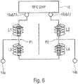
- An equivalent circuit of the RFIC element 100 configured in this manner is shown in Fig. 2 .
- An inductor L1 corresponds to the first coil portion CIL1
- an inductor L2 corresponds to the second coil portion CIL2.
- An inductor L3 corresponds to the third coil portion CIL3, and an inductor L4 corresponds to the fourth coil portion CIL4.
- the characteristics of impedance matching by the power feeding circuit 18 are specified by the values of the inductors L1 to L4.
- One end of the inductor L1 and one end of the inductor L2 are connected to the first input/output terminal 16a and the second input/output terminal 16b, respectively, disposed on the RFIC chip 16.
- the other end of the inductor L1 is connected to one end of the inductor L3, and the other end of the inductor L2 is connected to one end of the inductor L4.
- the other end of the inductor L3 is connected to the other end of the inductor L4.
- the first terminal electrode 14a is connected to a connection point between the inductors L1 and L3, and the second terminal electrode 14b is connected to a connection point between the inductors L2 and L4.
- the first coil portion CIL1, the second coil portion CIL2, the third coil portion CIL3, and the fourth coil portion CIL4 are wound to produce magnetic fields in phase and are connected in series to each other. Therefore, the magnetic fields are generated toward a direction indicted by arrows of Fig. 6 at a certain point in time and are generated toward a direction opposite to the arrows at another point in time.
- the first coil portion CIL1 and the third coil portion CIL3 include substantially the same loop shape and a same first winding axis
- the second coil portion CIL2 and the fourth coil portion CIL4 include substantially the same loop shape and a same second winding axis.
- the first winding axis and the second winding axis are disposed at positions such that the RFIC chip 16 is interposed therebetween.
- the first coil portion CIL1 and the third coil portion CIL3 are magnetically and capacitively coupled, and the second coil portion CIL2 and the fourth coil portion CIL4 are magnetically and capacitively coupled.
- the RFIC chip 16 includes the first input/output terminal 16a and the second input/output terminal 16b and is built into the multilayer substrate 12.
- the power feeding circuit 18 includes the coil patterns 20a to 20c and is built into the multilayer substrate 12.
- the coil pattern 20a includes the other end (the first coil end T1) connected to the first input/output terminal 16a
- the coil pattern 20b includes the other end (the second coil end T2) connected to the second input/output terminal 16b.
- the first terminal electrode 14a and the second terminal electrode 14b are disposed on the one principal surface of the multilayer substrate 12 and are connected to the one end of the coil pattern 20a (the first position P1) and the one end of the coil pattern 20b (the second position P2), respectively.
- the first coil portion CIL1 is disposed in a section extending from the first coil end T1 to the first position P1 and includes the first winding axis extending in the direction intersecting with the one principal surface of the multilayer substrate 12.
- the second coil portion CIL2 is disposed in a section extending from the second coil end T2 to the second position P2 and includes the second winding axis in the direction intersecting with the one principal surface of the multilayer substrate 12.
- the third coil portion CIL3 is disposed to overlap with the first coil portion CIL1 in the planar view and the fourth coil portion CIL4 is disposed to overlap with the second coil portion CIL2 in the planar view.
- the first coil portion CIL1/the third coil portion CIL3 and the second coil portion CIL2/the fourth coil portion CIL4 are disposed at positions such that the RFIC chip 16 is interposed therebetween in the planar view of the multilayer substrate 12.
- the RFIC chip 16 While the power feeding circuit 18 that provides impedance matching is built into the multilayer substrate 12, the RFIC chip 16 is also built into the multilayer substrate 12, and the first coil portion CIL1/the third coil portion CIL3 and the second coil portion CIL2/the fourth coil portion CIL4 are disposed at positions such that the RFIC chip 16 is interposed therebetween in the planar view of the multilayer substrate 12.
- the RFIC chip 16 since the RFIC chip 16 includes the semiconductor substrate, the RFIC chip 16 defines and functions as a ground or a shield for the first coil portion CIL1, the second coil portion CIL2, the third coil portion CIL3, and the fourth coil portion CIL4, so that the first coil portion CIL1 and the second coil portion CIL2 are not significantly magnetically or capacitively coupled to each other, and such that the third coil portion CIL3 and the fourth coil portion CIL4 are not significantly magnetically or capacitively coupled to each other. This reduces the risk of narrowing the passband of communication signals.
- FIG. 7A and 7B An example of an RFID tag including the RFIC module 10 of this embodiment mounted thereon is shown in Figs. 7A and 7B .
- This RFID tag is a dipole type RFID tag, and an antenna element 30a includes an antenna base material 32a and antenna conductors 34a, 34b disposed thereon.
- the antenna base material 32a is a belt-shaped flexible base material made of PET.
- Each of the antenna conductors 34a and 34b is a belt-shaped flexible conductor made of aluminum foil or copper foil.
- the antenna conductors 34a and 34b include a common width and length. The width of each of the antenna conductors 34a and 34b is less than the width of the antenna base material 32a, and the length of each of the antenna conductors 34a and 34b is less than a half of the length of the antenna base material 32a.
- the antenna conductors 34a and 34b are disposed on a surface of the antenna base material 32a (a surface facing toward the negative side in the Z-axis direction). Specifically, the antenna conductor 34a is disposed on a region of the surface of the antenna base material 32a on the negative side in the X-axis direction and extends in the longitudinal direction of the antenna base material 32a. Similarly, the antenna conductor 34b is disposed on a region of the surface of the antenna base material 32a on the positive side in the X-axis direction and extends in the longitudinal direction of the antenna base material 32a.
- An interval between one end of the antenna conductor 34a (an end portion on the positive side in the X-axis direction) and one end of the antenna conductor 34b (an end portion on the negative side in the X-axis direction) is matched to an interval between the first terminal electrode 14a and the second terminal electrode 14b disposed on the RFIC module 10.
- the RFIC module 10 is mounted on the surface of the antenna base material 32a at a center position in a posture with one principal surface thereof facing the surface of the antenna base material 32a.
- the first terminal electrode 14a is connected to the one end of the antenna conductor 34a
- the second terminal electrode 14b is connected to the one end of the antenna conductor 34b.
- the first terminal electrode 14a is fixed to the antenna conductor 34a by a conductive bonding material 36a
- the second terminal electrode 14b is fixed to the antenna conductor 34b by a conductive bonding material 36b (see Fig. 9 ).
- an insulation bonding material may be used to provide a capacitive connection.
- the first terminal electrode 14a and the second terminal electrode 14b may electrically be connected to the antenna conductors 34a and 34b.
- the multilayer substrate 12 is made of flexible polyimide or liquid crystal polymer, and the coil patterns 20a to 20c, the first terminal electrode 14a, and the second terminal electrode 14b are made of flexible copper foil.
- the interlayer connection conductors 22a, 22b, 24a, 24b are hard conductors made of Sn, and the substrate of the RFIC chip 16 is also a hard substrate made of silicon.
- the first and second terminal electrodes 14a, 14b including a large area reduce the flexibility of the copper foil, and the flexibility is eliminated by applying a plating film of Ni/Au or Ni/Sn etc.
- the respective regions disposed with the first terminal electrode 14a, the second terminal electrode 14b, and the RFIC chip 16 are define as the rigid regions, and the other regions are defined as the flexible regions.
- the flexible regions are provided between the first terminal electrode 14a and the RFIC chip 16 and between the second terminal electrode 14b and the RFIC chip 16.
- the interlayer connection conductors 22a, 22b, 24a, 24b are disposed in the rigid regions.
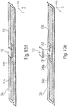
- the RFIC module 10 is bent as shown in Fig. 9 , for example.
- the RFIC chip 16 itself includes a parasitic capacitance (stray capacitance) Cp produced between the first input/output terminal 16a and the second input/output terminal 16b, and two resonances are generated in the RFIC module 10.
- the first resonance is the resonance generated in a current path including the antenna conductors 34a, 34b, the inductor L3, and the inductor L4, and the second resonance is the resonance generated in a current path (current loop) including the inductors L1 to L4 and the parasitic capacitance Cp.
- These two resonances are coupled by the inductors L3 to L4 shared by the current paths, and two respective currents I1 and I2 corresponding to the two resonances flow in a manner as shown in Fig. 10 .
- Both of a first resonance frequency and a second resonance frequency are affected by the inductors L3 to L4.
- a difference of several dozen MHz (specifically, about 5 MHz to 50 MHz) is generated between the first resonance frequency and the second resonance frequency.
- the resonance frequency characteristics thereof are represented by curves A and B in Fig. 11 .
- broadband resonance frequency characteristics are produced as indicated by a curve C in Fig. 11 .
- FIG. 12 Another example of an RFID tag including the RFIC module 10 of this embodiment mounted thereon is shown in Fig. 12 .
- This RFID tag is the same as the RFID tag shown in Figs. 7A to 7B except that a magnet 36 is provided on the back surface of the antenna base material 32a (the surface facing toward the positive side in the Z-axis direction). As a result, the RFID tag is able to be easily affixed to an object made of metal.
- an antenna element 30c includes an antenna base material 32b and an antenna conductor 34c disposed thereon.
- the antenna base material 32b is a belt-shaped flexible base material made of PET
- the antenna conductor 34c is a belt-shaped flexible conductor made of aluminum foil or copper foil.
- a rectangular through-hole HL2 is disposed with long sides extending along the belt, and a cutout CT1 is disposed from an outer edge of the belt to the through-hole HL2.
- the length of the through-hole HL2 is greater than the length of the RFIC module 10, while the length of the cutout CT1 is less than the length of the RFIC module 10.
- the RFIC module 10 is mounted at a position covering the cutout CT1 with one principal surface thereof facing the surface of the antenna base material 32b.
- the first terminal electrode 14a is connected to one end of the loop conductor 341p
- the second terminal electrode 14b is connected to the other end of the loop conductor 341p.
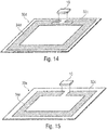
- an antenna element 30d includes a square antenna base material 32c and an antenna conductor 34d disposed thereon.
- the antenna conductor 34d is defined by coupling the antenna conductors 34c shown in Figs. 13A to 13B into a loop shape. As a result, the antenna conductor 34d defines and functions as a loop antenna.
- an antenna element 30e includes a square antenna base material 32c and an antenna conductor 34e disposed thereon.
- the antenna conductor 34e is defined by coupling the antenna conductors 34a and 34b shown in Figs. 7A to 7B into a loop shape.
- the antenna conductor 34e also defines and functions as a loop antenna.
- the RFID tag shown in Fig. 14 or 15 is attached to a cylindrical article 40 in a manner shown in Fig. 16 .
- the article 40 may be a PET bottle or a flexible pack for drip infusion, for example, and Fig. 16 shows an attached state of the RFID tag shown in Fig. 15 .
- a loop antenna includes no open end. Therefore, the antenna characteristics are not adversely affected by the permittivity of an object to which the antenna is affixed, i.e., the article 40.
- FIG. 17A to 17C Another example of the multilayer substrate 12 of the RFIC module 10 is shown in Figs. 17A to 17C .
- the main differences from the multilayer substrate 12 shown in Figs. 4A to 4C are in the respective winding directions of a first coil portion CIL11 and a second coil portion CIL21, the respective winding numbers and winding directions of third coil portions CIL31 and CIL41, a positional relationship in a planar view between the center of the opening of the first coil portion CIL11 and a first terminal electrode 141a, and the positional relationship in a planar view between the center of opening of the second coil portion CIL21 and a second terminal electrode 141b.
- the multilayer substrate 12 includes three laminated sheet-shaped insulation layers 121a to 121c.
- the insulation layer 121a is an upper layer
- the insulation layer 121b is an intermediate layer
- the insulation layer 121c is a lower layer.
- the first terminal electrode 141a and the second terminal electrode 141b are provided on one principal surface of the insulation layer 121a.
- the first terminal electrode 141a is disposed on the negative side in the X-axis direction and the second terminal electrode 141b is disposed on the positive side in the X-axis direction.
- a rectangular through-hole HL11 is provided, which extends to the other principal surface.
- the size of the through-hole HL11 is matched to the size of an RFIC chip 161.
- a coil pattern 201c made of flexible copper foil and extending in a belt shape is provided around the through-hole HL11 on the one principal surface of the insulation layer 121b.
- One end of the coil pattern 201c is disposed at a position overlapping with the first terminal electrode 141a in the planar view and is connected to the first terminal electrode 141a by an interlayer connection conductor 221a extending in the Z-axis direction.
- the other end of the coil pattern 201c is disposed at a position overlapping with the second terminal electrode 141b in the planar view and is connected to the second terminal electrode 141b by an interlayer connection conductor 221b extending in the Z-axis direction.
- the interlayer connection conductors 221a, 221b and interlayer connection conductors 241a, 241b described later are hard metal masses containing Sn as a main component.
- the coil pattern 201c winds around the one end once in the clockwise direction, extends to near the end portion of the positive side in the Y-axis direction, and then extends into the positive side in the X-axis direction.
- the coil pattern 201c subsequently bends near the end portion of the positive side in the X-axis direction toward the negative side in the Y-axis direction and winds around the other end once in the clockwise direction before extending to the other end.
- Coil patterns 201a and 201b made of flexible copper foil and extending in a belt shape are provided on one principal surface of the insulation layer 121c.
- one end of the coil pattern 201a is disposed at a position on the positive side in the Y-axis direction as compared to the one end of the coil pattern 201c, and the other end of the coil pattern 201a (a first coil end T11) is disposed at a position on the negative side in the X-axis direction inside a rectangular shape defined by the through-hole HL11.
- One end of the coil pattern 201b is disposed at a position on the positive side in the Y-axis direction as compared to the other end of the coil pattern 201c, and the other end of the coil pattern 201b (a second coil end T21) is disposed at a position on the positive side in the X-axis direction inside the rectangular shape defined by the through-hole HL11.
- Both of the first coil end T11 and the second coil end T21 have a rectangular shape with the long sides extending in the Y-axis direction in the planar view of the insulation layer 121c.
- the coil pattern 201a winds around the one end 2. 5 times in the counterclockwise direction and subsequently bends toward the positive side in the Y-axis direction to reach the other end.
- the coil pattern 201b winds around the one end 2.5 times in the clockwise direction and subsequently bends toward the positive side in the Y-axis direction to extend to the other end.
- the one end of the coil pattern 201a is connected to the one end of the coil pattern 201c by the interlayer connection conductor 241a extending in the Z-axis direction
- the one end of the coil pattern 201b is connected to the other end of the coil pattern 201c by the interlayer connection conductor 241b extending in the Z-axis direction.
- the power feeding circuit 18 includes the coil patterns 201a to 201c and the interlayer connection conductors 241a and 241b arranged in this manner.
- a conductor portion of the coil pattern 201a except the first coil end T11 is defined as the "first coil portion CIL11” and a conductor portion of the coil pattern 201b except the second coil end T21 is defined as the "second coil portion CIL21.”
- a conductor portion of the coil pattern 201c on the negative side in the X-axis direction relative to the through-hole HL11 is defined as the "third coil portion CIL31" and a conductor portion of the coil pattern 201c on the positive side in the X-axis direction relative to the through-hole HL11 is defined as the "fourth coil portion CIL41.”
- the position of the one end of the coil pattern 201a or the one end of the coil pattern 201c corresponds to the "first position P1" and the position of the one end of the coil pattern 201b or the other end of the coil pattern 201c corresponds to the "second position P2.”
- a first input/output terminal 161a and a second input/output terminal 161b are disposed on the other principal surface of the RFIC chip 161. Specifically, the first input/output terminal 161a is located on the negative side in the X-axis direction, and the second input/output terminal 161b is located on the positive side in the X-axis direction.
- the RFIC chip 161 is mounted on the one principal surface of the insulation layer 121c such that the first input/output terminal 161a and the second input/output terminal 161b arranged in this manner are connected to the first coil end T11 and the second coil end T21.
- the distance from the first terminal electrode 141a to the first coil portion CIL11 is greater than the distance from the first terminal electrode 141a to the third coil portion CIL31, and the distance from the second terminal electrode 141b to the second coil portion CIL21 is greater than the distance from the second terminal electrode 141b to the fourth coil portion CIL41.
- the winding number of the first coil portion CIL11 is greater than the winding number of the third coil portion CIL31, and the winding number of the second coil portion CIL21 is greater than the winding number of the fourth coil portion CIL41.
- the inductance value of the first coil portion CIL11 is greater than the inductance value of the third coil portion CIL31
- the inductance value of the second coil portion CIL21 is greater than the inductance value of the fourth coil portion CIL41.
- the first terminal electrode 141a When viewed in the Z-axis direction, the first terminal electrode 141a does not overlap with the respective opening centers of the first coil portion CIL11 and the third coil portion CIL31, and the second terminal electrode 141b does not overlap with the respective opening centers of the second coil portion CIL21 and the fourth coil portion CIL41.
- This configurations reduces the risk of the first terminal electrode 141a disturbing the magnetic field generation by the first coil portion CIL11 and the third coil portion CIL31, and also reduces the risk of the second terminal electrode 141b disturbing the magnetic field generation by the second coil portion CIL21 and the fourth coil portion CIL41.
- the risk of disturbing the magnetic field generation is further reduced by completely eliminating the overlap of the respective openings of the first coil portion CIL11 and the third coil portion CIL31 with the first terminal electrode 141a and by completely eliminating the overlap of the respective openings of the second coil portion CIL21 and the fourth coil portion CIL41 with the second terminal electrode 141b.
- FIGs. 18A to 18C Yet another example of the multilayer substrate 12 of the RFIC module 10 is shown in Figs. 18A to 18C .
- the main differences from the multilayer substrate 12 shown in Figs. 17A to 17C are in the respective winding numbers and opening areas of a first coil portion CIL12 and a second coil portion CIL22, the respective opening areas of a third coil portion CIL32 and a fourth coil portion CIL42, and the arrangement of the interlayer connection conductors 221a to 221b, 241a to 241b.
- the multilayer substrate 12 includes three laminated sheet-shaped insulation layers 122a to 122c.
- the insulation layer 122a is an upper layer
- the insulation layer 122b is an intermediate layer
- the insulation layer 122c is a lower layer.
- a first terminal electrode 142a and a second terminal electrode 142b are provided on one principal surface of the insulation layer 122a.
- the first terminal electrode 142a is disposed on the negative side in the X-axis direction and the second terminal electrode 142b is disposed on the positive side in the X-axis direction.
- a rectangular through-hole HL12 is provided, and extends the other principal surface.
- the size of the through-hole HL12 is matched to the size of an RFIC chip 162.
- a coil pattern 202c made of flexible copper foil and extending in a belt shape is provided around the through-hole HL12 on the one principal surface of the insulation layer 122b.
- One end of the coil pattern 202c is disposed at a position overlapping with the first terminal electrode 142a in the planar view and is connected to the first terminal electrode 142a by an interlayer connection conductor 222a extending in the Z-axis direction.
- the other end of the coil pattern 202c is disposed at a position overlapping with the second terminal electrode 142b in the planar view and is connected to the second terminal electrode 142b by an interlayer connection conductor 222b extending in the Z-axis direction.
- the interlayer connection conductors 222a, 222b and interlayer connection conductors 242a, 242b described later are hard metal masses containing Sn as a main component.
- the coil pattern 202c winds around the one end once in the clockwise direction, extends to near the end portion of the positive side in the Y-axis direction, and then extends into the positive side in the X-axis direction.
- the coil pattern 202c subsequently bends near the end portion of the positive side in the X-axis direction toward the negative side in the Y-axis direction and winds around the other end once in the clockwise direction before extending to the other end.
- Coil patterns 202a and 202b made of flexible copper foil and extending in a belt shape are provided on one principal surface of the insulation layer 122c.
- one end of the coil pattern 202a is disposed at a position overlapping with the one end of the coil pattern 202c, and the other end of the coil pattern 202a (a first coil end T12) is disposed at a position on the negative side in the X-axis direction inside a rectangular shape defined by the through-hole HL12.
- One end of the coil pattern 202b is disposed at a position overlapping with the other end of the coil pattern 202c, and the other end of the coil pattern 202b (a second coil end T22) is disposed at a position on the positive side in the X-axis direction inside the rectangular shape defined by the through-hole HL12.
- Both of the first coil end T12 and the second coil end T22 define a rectangle with the long sides extending in the Y-axis direction in the planar view of the insulation layer 122c.
- the coil pattern 202a winds around the one end 1.5 times in the counterclockwise direction and subsequently bends toward the positive side in the Y-axis direction to reach the other end.
- the coil pattern 202b winds around the one end 1.5 times in the clockwise direction and subsequently bends toward the positive side in the Y-axis direction to reach the other end.
- the one end of the coil pattern 202a is connected to the one end of the coil pattern 202c by the interlayer connection conductor 242a extending in the Z-axis direction
- the one end of the coil pattern 202b is connected to the other end of the coil pattern 202c by the interlayer connection conductor 242b extending in the Z-axis direction.
- the power feeding circuit 18 includes the coil patterns 202a to 202c and the interlayer connection conductors 242a and 242b arranged in this manner.
- a conductor portion of the coil pattern 202a except the first coil end T12 is defined as the "first coil portion CIL12" and a conductor portion of the coil pattern 202b except the second coil end T22 is defined as the "second coil portion CIL22.”
- a conductor portion of the coil pattern 202c on the negative side in the X-axis direction relative to the through-hole HL12 is defined as the "third coil portion CIL32" and a conductor portion of the coil pattern 202c on the positive side in the X-axis direction relative to the through-hole HL12 is defined as the "fourth coil portion CIL42.”
- the position of the one end of the coil pattern 202a or the one end of the coil pattern 202c corresponds to the "first position P1" and the position of the one end of the coil pattern 202b or the other end of the coil pattern 202c corresponds to the "second position P2.”
- a first input/output terminal 162a and a second input/output terminal 162b are disposed on the other principal surface of the RFIC chip 162. Specifically, the first input/output terminal 162a is located on the negative side in the X-axis direction, and the second input/output terminal 162b is located on the positive side in the X-axis direction.
- the RFIC chip 162 is mounted on the one principal surface of the insulation layer 122c such that the first input/output terminal 162a and the second input/output terminal 162b arranged in this manner are connected to the first coil end T12 and the second coil end T22.
- the opening area and the opening center of the third coil portion CIL32 are substantially identical to the opening area and the opening center of the first coil portion CIL12.
- the opening area and the opening center of the fourth coil portion CIL42 are substantially identical to the opening area and the opening center of the second coil portion CIL22.
- the opening center of the first coil portion CIL12 and the opening center of the third coil portion CIL32 do not overlap with the first terminal electrode 142a and, similarly, the opening center of the second coil portion CIL22 and the opening center of the fourth coil portion CIL42 do not overlap with the second terminal electrode 142b.
- the magnetic field produced by the first coil portion CIL12 and the third coil portion CIL32 becomes stable and, similarly, the magnetic field produced by the second coil portion CIL22 and the fourth coil portion CIL42 becomes stable.
- FIGs. 19A to 19C A further example of the multilayer substrate 12 of the RFIC module 10 is shown in Figs. 19A to 19C .
- the main differences from the multilayer substrate 12 shown in Figs. 17A to 17C are in the respective opening areas of the third coil portion CIL32 and the fourth coil portion CIL42.
- the multilayer substrate 12 includes three laminated sheet-shaped insulation layers 123a to 123c.
- the insulation layer 123a is an upper layer
- the insulation layer 123b is an intermediate layer
- the insulation layer 123c is a lower layer.
- a first terminal electrode 143a and a second terminal electrode 143b are provided on one principal surface of the insulation layer 123a.
- the first terminal electrode 143a is disposed on the negative side in the X-axis direction and the second terminal electrode 143b is disposed on the positive side in the X-axis direction.
- a rectangular through-hole HL13 is provided, and extends to the other principal surface.
- the size of the through-hole HL13 is matched to the size of an RFIC chip 163.
- a coil pattern 203c made of flexible copper foil and extending in a belt shape is provided around the through-hole HL13 on the one principal surface of the insulation layer 123b.
- One end of the coil pattern 203c is disposed at a position overlapping with the first terminal electrode 143a in the planar view and is connected to the first terminal electrode 143a by an interlayer connection conductor 223a extending in the Z-axis direction.
- the other end of the coil pattern 203c is disposed at a position overlapping with the second terminal electrode 143b in the planar view and is connected to the second terminal electrode 143b by an interlayer connection conductor 223b extending in the Z-axis direction.
- the interlayer connection conductors 223a, 223b and interlayer connection conductors 243a, 243b described later are hard metal masses containing Sn as a main component.
- the coil pattern 203c winds around the one end once in the clockwise direction, extends to near the end portion of the positive side in the Y-axis direction, and then extends into the positive side in the X-axis direction.
- the coil pattern 203c subsequently bends near the end portion of the positive side in the X-axis direction toward the negative side in the Y-axis direction and winds around the other end once in the clockwise direction before extending to the other end.
- Coil patterns 203a and 203b made of flexible copper foil and extending in a belt shape are provided on one principal surface of the insulation layer 123c.
- one end of the coil pattern 203a is disposed at a position on the positive side in the Y-axis direction as compared to the one end of the coil pattern 203c, and the other end of the coil pattern 203a (a first coil end T13) is disposed at a position on the negative side in the X-axis direction inside a rectangular shape defined by the through-hole HL13.
- One end of the coil pattern 203b is disposed at a position on the positive side in the Y-axis direction as compared to the other end of the coil pattern 203c, and the other end of the coil pattern 203b (a second coil end T23) is disposed at a position on the positive side in the X-axis direction inside the rectangular shape defined by the through-hole HL13.
- Both of the first coil end T13 and the second coil end T23 have a rectangular shape with the long sides extending in the Y-axis direction in the planar view of the insulation layer 123c.
- the coil pattern 203a winds around the one end 2. 5 times in the counterclockwise direction and subsequently bends toward the positive side in the Y-axis direction to extend to the other end.
- the coil pattern 203b winds around the one end 2.5 times in the clockwise direction and subsequently bends toward the positive side in the Y-axis direction to extend to the other end.
- the one end of the coil pattern 203a is connected to the one end of the coil pattern 203c by the interlayer connection conductor 243a extending in the Z-axis direction
- the one end of the coil pattern 203b is connected to the other end of the coil pattern 203c by the interlayer connection conductor 243b extending in the Z-axis direction.
- the power feeding circuit 18 includes the coil patterns 203a to 203c and the interlayer connection conductors 243a and 243b arranged in this manner.
- a conductor portion of the coil pattern 203a except the first coil end T13 is defined as a "first coil portion CIL13”
- a conductor portion of the coil pattern 203b except the second coil end T23 is defined as a "second coil portion CIL23.”
- a conductor portion of the coil pattern 203c on the negative side in the X-axis direction relative to the through-hole HL13 is defined as a "third coil portion CIL33" and a conductor portion of the coil pattern 203c on the positive side in the X-axis direction relative to the through-hole HL13 is defined as a "fourth coil portion CIL43.”
- the position of the one end of the coil pattern 203a or the one end of the coil pattern 203c corresponds to the "first position P1" and the position of the one end of the coil pattern 203b or the other end of the coil pattern 203c corresponds to the "second position P2.”
- a first input/output terminal 163a and a second input/output terminal 163b are disposed on the other principal surface of the RFIC chip 163. Specifically, the first input/output terminal 163a is located on the negative side in the X-axis direction, and the second input/output terminal 163b is located on the positive side in the X-axis direction.
- the RFIC chip 163 is mounted on the one principal surface of the insulation layer 123c such that the first input/output terminal 163a and the second input/output terminal 163b arranged in this manner are connected to the first coil end T13 and the second coil end T23.
- this multilayer substrate 12 also includes the inductance value of the first coil portion CIL13 greater than the inductance value of the third coil portion CIL33 and the inductance value of the second coil portion CIL23 greater than the inductance value of the fourth coil portion CIL43.
- the opening center of the first coil portion CIL13 and the opening center of the third coil portion CIL33 do not overlap with the first terminal electrode 143a and, similarly, the opening center of the second coil portion CIL23 and the opening center of the fourth coil portion CIL43 do not overlap with the second terminal electrode 143b.
- the opening area of the third coil portion CIL33 is greater than the opening area of the third coil portion CIL31 shown in Fig. 17B
- the opening area of the fourth coil portion CIL43 is greater than the opening area of the fourth coil portion CIL41 shown in Fig. 17B .
- the magnetic field produced by the first coil portion CIL11 and the third coil portion CIL31 and the magnetic field produced by the second coil portion CIL21 and the fourth coil portion CIL41 become greater than those of the multilayer substrate 12 shown in Figs. 17A to 17C .
- FIGs. 20A to 20C Yet another example of the multilayer substrate 12 of the RFIC module 10 is shown in Figs. 20A to 20C .
- the main differences from the multilayer substrate 12 shown in Figs. 14A to 14C are in the respective opening areas of a first coil portion CIL14 and a second coil portion CIL24, the respective winding numbers and opening areas of the third coil portion CIL32 and the fourth coil portion CIL42, and the arrangement of the interlayer connection conductors 224a to 224b, 244a to 244b.
- the multilayer substrate 12 includes three laminated sheet-shaped insulation layers 124a to 124c.
- the insulation layer 124a is an upper layer
- the insulation layer 124b is an intermediate layer
- the insulation layer 124c is a lower layer.
- a first terminal electrode 144a and a second terminal electrode 144b are provided on one principal surface of the insulation layer 124a.
- the first terminal electrode 144a is disposed on the negative side in the X-axis direction and the second terminal electrode 144b is disposed on the positive side in the X-axis direction.
- a rectangular through-hole HL14 is provided, extends to the other principal surface.
- the size of the through-hole HL14 is matched to the size of an RFIC chip 164.
- a coil pattern 204c made of flexible copper foil and extending in a belt shape is provided around the through-hole HL14 on the one principal surface of the insulation layer 124b.
- One end of the coil pattern 204c is disposed at a position overlapping with the first terminal electrode 144a in the planar view and is connected to the first terminal electrode 144a by the interlayer connection conductor 224a extending in the Z-axis direction.
- the other end of the coil pattern 204c is disposed at a position overlapping with the second terminal electrode 144b in the planar view and is connected to the second terminal electrode 144b by the interlayer connection conductor 224b extending in the Z-axis direction.
- the interlayer connection conductors 224a, 224b and the interlayer connection conductors 244a, 244b described later are hard metal masses containing Sn as a main component.
- the coil pattern 204c winds around the one end twice in the clockwise direction, extends to near the end portion of the positive side in the Y-axis direction, and then extends into the positive side in the X-axis direction.
- the coil pattern 204c subsequently bends near the end portion of the positive side in the X-axis direction toward the negative side in the Y-axis direction and winds around the other end twice in the clockwise direction before extending to the other end.
- Coil patterns 204a and 204b made of flexible copper foil and extending in a belt shape are provided on one principal surface of the insulation layer 124c.
- one end of the coil pattern 204a is disposed at a position overlapping with the one end of the coil pattern 204c, and the other end of the coil pattern 204a (a first coil end T14) is disposed at a position on the negative side in the X-axis direction inside a rectangular shape defined by the through-hole HL14.
- One end of the coil pattern 204b is disposed at a position overlapping with the other end of the coil pattern 204c, and the other end of the coil pattern 204b (a second coil end T24) is disposed at a position on the positive side in the X-axis direction inside the rectangular shape defined by the through-hole HL14.
- Both of the first coil end T14 and the second coil end T24 have a rectangular shape with the long sides extending in the Y-axis direction in the planar view of the insulation layer 124c.
- the coil pattern 204a winds around the one end 2. 5 times in the counterclockwise direction and subsequently bends toward the positive side in the Y-axis direction to extend to the other end.
- the coil pattern 204b winds around the one end 2.5 times in the clockwise direction and subsequently bends toward the positive side in the Y-axis direction to extend to the other end.
- the one end of the coil pattern 204a is connected to the one end of the coil pattern 204c by the interlayer connection conductor 244a extending in the Z-axis direction
- the one end of the coil pattern 204b is connected to the other end of the coil pattern 202c by the interlayer connection conductor 244b extending in the Z-axis direction.
- the power feeding circuit 18 includes the coil patterns 204a to 204c and the interlayer connection conductors 244a and 244b arranged in this manner.
- a conductor portion of the coil pattern 204a except the first coil end T14 is defined as the "first coil portion CIL14" and a conductor portion of the coil pattern 204b except the second coil end T24 is defined as the "second coil portion CIL24.”
- a conductor portion of the coil pattern 204c on the negative side in the X-axis direction relative to the through-hole HL14 is defined as a "third coil portion CIL34" and a conductor portion of the coil pattern 204c on the positive side in the X-axis direction relative to the through-hole HL14 is defined as a "fourth coil portion CIL44.”
- the position of the one end of the coil pattern 204a or the one end of the coil pattern 204c corresponds to the "first position P1" and the position of the one end of the coil pattern 204b or the other end of the coil pattern 204c corresponds to the "second position P2.”
- a first input/output terminal 164a and a second input/output terminal 164b are disposed on the other principal surface of the RFIC chip 164.
- the first input/output terminal 164a is located on the negative side in the X-axis direction
- the second input/output terminal 164b is located on the positive side in the X-axis direction.
- the RFIC chip 164 is mounted on the one principal surface of the insulation layer 124c such that the first input/output terminal 164a and the second input/output terminal 164b arranged in this manner are connected to the first coil end T14 and the second coil end T24.
- the winding number of the third coil portion CIL34 is greater than the winding number of the third coil portion CIL31
- the winding number of the fourth coil portion CIL44 is greater than the winding number of the fourth coil portion CIL41.
- the opening area of the first coil portion CIL14 is smaller than the opening area of the first coil portion CIL11, and the opening area of the second coil portion CIL24 is smaller than the opening area of the second coil portion CIL21.
- the opening center of the first coil portion CIL14 and the opening center of the third coil portion CIL34 do not overlap with the first terminal electrode 144a, and the opening center of the second coil portion CIL24 and the opening center of the fourth coil portion CIL44 do not overlap with the second terminal electrode 144b.
- the magnetic field produced by the first coil portion CIL14 and the third coil portion CIL34 becomes stable and, similarly, the magnetic field produced by the second coil portion CIL24 and the fourth coil portion CIL44 becomes stable.
- an RFIC module 10' of this embodiment is the same as the RFIC module 10 shown in Fig. 1 except that the first terminal electrode 14a, the second terminal electrode 14b, and the interlayer connection conductors 22a, 22b shown in Fig. 4A are removed and, therefore, the same constituent elements will not be described again.
- the inductors L1 and L2 affect the resonance frequency
- the first coil portion CIL1 and the second coil portion CIL2 corresponding to the respective inductors L1 and L2 define and function as an antenna element.
- the RFIC module 10' does not include two terminal electrodes to be connected to the antenna conductors 34a and 34b shown in Figs. 7A to 7B and also does not include interlayer connection conductors to be extended from the connection points of the first coil portion CIL1 and the third coil portion CIL3 and interlayer connection conductors to be extended from the connection points of the second coil portion CIL2 and the fourth coil portion CIL4.
- a small-sized RFID tag is provided.
- the RFIC module 10' is able to be included in the multilayer substrate 12 shown in Figs. 17A to 17C with the first terminal electrode 141a, the second terminal electrode 141b, and the interlayer connection conductors 221a, 221b removed, is able to be included in the multilayer substrate 12 shown in Figs. 18A to 18C with the first terminal electrode 142a, the second terminal electrode 142b, and the interlayer connection conductors 222a, 222b removed, is able to be included in the multilayer substrate 12 shown in Figs.
- the multilayer substrate 12 shown in Figs. 17A to 17C including the first terminal electrode 141a, the second terminal electrode 141b, and the interlayer connection conductors 221a, 221b removed is shown in Figs. 23A to 23C .
Landscapes
- Engineering & Computer Science (AREA)
- Power Engineering (AREA)
- Microelectronics & Electronic Packaging (AREA)
- Physics & Mathematics (AREA)
- Computer Hardware Design (AREA)
- General Physics & Mathematics (AREA)
- Theoretical Computer Science (AREA)
- Computer Networks & Wireless Communication (AREA)
- Electromagnetism (AREA)
- Details Of Aerials (AREA)
- Coils Or Transformers For Communication (AREA)
Abstract


Description
- The present invention relates to an RFIC (Radio Frequency Integrated Circuit) module and an RFID (Radio Frequency IDentifier) tag including the same and, more particularly, to an RFIC module and an RFID tag including an RFIC chip that includes two input/output terminals and a coil conductor that includes two coil ends respectively connected to the two input/output terminals.
- For an article information management system, an RFID system has recently been used and the RFID system enables a reader/writer and an RFID tag applied to an article to communicate in a non-contact manner utilizing a magnetic field or an electromagnetic field so as to transmit predetermined information. This RFID tag includes an RFIC chip storing predetermined information and processing a predetermined radio signal and an antenna element (radiator) transmitting/receiving high-frequency signals and is affixed to various articles (or packing materials thereof) to be managed when used.
- The RFID system is typically an HF band RFID system using the 13.56 MHz band or a UHF band RFID system using the 900 MHz band. Particularly, because of a comparatively long communication distance and an ability to read multiple tags together, the UHF band RFID system is considered as a promising system for article management. A tag having a structure disclosed in Patent Document 1 (
WO 2010/146944 ) is known as the UHF band RFID tag. - Patent Document 1:
WO 2010/146944 - The RFID tag of Patent Document 1 includes two coil conductors adjacently arranged in a ceramic multilayer substrate and a stray capacitance is easily provided between the two coil conductors. If the coil conductors are coupled via the stray capacitance, a resonance circuit defined by a stray capacitance component and the inductance components of the coil conductors is provided, so that a passband width may be narrowed.
- It is therefore a primary object of the present invention to provide an RFIC module and an RFID tag including the same capable of reducing the risk of narrowing the passband width.
- An RFIC module according to the present invention is an RFIC module comprising an RFIC chip mounted on a substrate and including a first input/output terminal and a second input/output terminal; a power feeding circuit built into the substrate and including a coil conductor including a first coil end and a second coil end respectively connected to the first input/output terminal and the second input/output terminal; a first terminal electrode disposed on a principal surface of the substrate and connected to a first position of the coil conductor; and a second terminal electrode disposed on the principal surface of the substrate and connected to a second position of the coil conductor, the coil conductor including a first coil portion and a second coil portion, the first coil portion being disposed in a section extending from the first coil end to the first position, the first coil portion including a first winding axis extending in a direction intersecting with the principal surface of the substrate, the second coil portion being disposed in a section extending from the second coil end to the second position, the second coil portion including a second winding axis in a direction intersecting with the principal surface of the substrate, the first coil portion, the second coil portion, the first winding axis, and the second winding axis being located at positions with the RFIC chip interposed therebetween in a planar view of the substrate.
- For the first coil portion and the second coil portion, the RFIC chip defines and functions as a ground or a shield, so that the first coil portion and the second coil portion are not significantly magnetically or capacitively coupled to each other. This enables a reduction in the risk of narrowing the passband of communication signals.
- Preferably, the RFIC chip is built into the substrate, and the power feeding circuit is disposed at a position overlapping with the RFIC chip when viewed in a direction perpendicular to a predetermined side surface of the substrate. This results to an increase in the shield effect due to the RFIC chip.
- Preferably, the substrate is a flexible substrate with the principal surface having a rectangle, and the first coil portion and the second coil portion are respectively located on opposing end sides of the long sides drawing the rectangle. This produces a thin flexible large-area RFIC chip module.
- Preferably, the first coil portion and the second coil portion are located at respective positions spaced away from the RFIC chip in a planar view of the substrate. This increases the shield effect due to the RFIC chip.
- Preferably, the first coil portion and the second coil portion are connected and wound such that magnetic fields generated by the respective coil portions are in phase. As a result, the first coil portion and the second coil portion are not significantly coupled through the magnetic fields.
- Preferably, in a planar view of the substrate, the first terminal electrode dose not overlap with a center of a coil opening of the first coil portion and the second terminal electrode does not overlap with a center of a coil opening of the second coil portion. As a result, the magnetic field generated by the first coil portion and the second coil portion is not significantly disturbed by the first terminal electrode and the second terminal electrode.
- Preferably, the coil conductor further includes a third coil portion and a fourth coil portion connected in series between the first position and the second position and respectively overlapping with the first coil portion and the second coil portion in a planar view of the substrate. The additional resonance produced by the parasitic capacitance between the first coil portion and the second coil portion is coupled to the resonance produced by the third coil portion and the fourth coil portion. As a result, broadband resonance frequency characteristics are achieved.
- In a certain aspect, the power feeding circuit further includes a first connection conductor extending in a thickness direction of the substrate at a position overlapping with the first terminal electrode in a planar view of the substrate to connect the first coil portion and the third coil portion in series and a second connection conductor extending in a thickness direction of the substrate at a position overlapping with the second terminal electrode in a planar view of the substrate to connect the second coil portion and the fourth coil portion in series. The first connection conductor and the second connection conductor are disposed in a rigid area of the substrate in the planar view. This prevents a reduction in the flexibility of the RFIC module.
- In another aspect, the first coil portion, the second coil portion, the third coil portion, and the fourth coil portion are connected and wound such that magnetic fields generated by the coil conductor are in phase among the first coil portion, the second coil portion, the third coil portion, and the fourth coil portion. This increases the magnetic field strength.
- Preferably, the third coil portion and the fourth coil portion are disposed on a layer adjacent to a layer on which the first and second terminal electrodes are provided, and the first coil portion and the second coil portion are disposed on a layer that is adjacent to the layer on which the third coil portion and the fourth coil portion are disposed on the side opposite to the layer on which the first and second terminal electrodes are provided.
- As a result, the first coil portion and the second coil portion are disposed at positions spaced further away from the first terminal electrode and the second terminal electrode as compared to the third coil portion and the fourth coil portion. Therefore, even if the inductance values of the first coil portion and the second coil portion are increased, the magnetic field generation by the first coil portion and the second coil portion is not significantly disturbed by the first terminal electrode and the second terminal electrode.
- More preferably, the inductance values of the first coil portion and the second coil portion are larger than the inductance values of the third coil portion and the fourth coil portion, respectively. Such a structure increases the significance of disposing the first coil portion and the second coil portion at positions spaced away from the first terminal electrode and the second terminal electrode.
- An RFID tag according to the present invention is an RFID tag comprising an RFIC module; and an antenna element connected to the RFIC module, the RFIC module including an RFIC chip mounted on a substrate and including a first input/output terminal and a second input/output terminal, a power feeding circuit built into the substrate and including a coil conductor including a first coil end and a second coil end respectively connected to the first input/output terminal and the second input/output terminal, a first terminal electrode disposed on a principal surface of the substrate and connected to a first position of the coil conductor, and a second terminal electrode disposed on the principal surface of the substrate and connected to a second position of the coil conductor, the coil conductor including a first coil portion and a second coil portion, the first coil portion being disposed in a section extending from the first coil end to the first position, the first coil portion including a first winding axis extending in a direction intersecting with the principal surface of the substrate, the second coil portion being disposed in a section extending from the second coil end to the second position, the second coil portion including a second winding axis extending in a direction intersecting with the principal surface of the substrate, the first coil portion and the second coil portion as well as the first winding axis and the second winding axis being located at positions with the RFIC chip interposed therebetween in a planar view of the substrate.
- For the first coil portion and the second coil portion, the RFIC chip defines and functions as a ground or a shield, so that the first coil portion and the second coil portion are not significantly magnetically or capacitively coupled to each other. This enables a reduction in the risk of narrowing the passband of communication signals.
- Preferably, the antenna element is a dipole type antenna element including a first antenna portion connected at one end to the first terminal electrode and a second antenna portion connected at one end to the second terminal electrode. As a result, the RFID tag is able to be easily produced.
- Preferably, the antenna element is a loop type antenna element including one end connected to the first terminal electrode and the other end connected to the second terminal electrode. As a result, the antenna characteristics are not significantly varied by the permittivity of an article to which the RFID tag is affixed.
- An RFIC module of the present invention is an RFIC module comprising an RFIC chip mounted on a substrate and including a first input/output terminal and a second input/output terminal; and a power feeding circuit built into the substrate and including a coil conductor including a first coil end and a second coil end respectively connected to the first input/output terminal and the second input/output terminal, the coil conductor including a first coil portion and a second coil portion connected in series and located at positions with the RFIC chip interposed therebetween in a planar view of the substrate, the first coil portion and the second coil portion respectively including a first winding axis and a second winding axis with the RFIC chip interposed therebetween in a planar view of the substrate, the first winding axis and the second winding axis extending in a direction intersecting with the principal surface.
- For the first coil portion and the second coil portion, the RFIC chip defines and functions as a ground or a shield, so that the first coil portion and the second coil portion are not significantly magnetically or capacitively coupled to each other. This enables a reduction in the risk of narrowing the passband of communication signals. The first coil portion and the second coil portion define and function as an antenna element and, therefore, a small-sized RFID tag is achieved.
- Preferably, the coil conductor further includes a third coil portion and a fourth coil portion connected in series between the first coil portion and the second coil portion and respectively overlapping with the first coil portion and the second coil portion in a planar view of the substrate.
- The additional resonance produced by the parasitic capacitance between the first coil portion and the second coil portion is coupled to the resonance produced by the third coil portion and the fourth coil portion. As a result, broadband resonance frequency characteristics are achieved.
- According to the present invention, the risk of narrowing the passband of communication signals is able to be reduced by enabling the RFIC chip to define and function as a ground or a shield.
- The above object, other objects, characteristics, and advantages of the present invention will become more apparent from the following embodiments described in detail with reference to the attached drawings.
-
-
Fig. 1 is a perspective view of an RFID tag of this embodiment viewed obliquely from above. -
Fig. 2 is a circuit diagram of an equivalent circuit of the RFIC module. -
Fig. 3A is a top view of the RFIC module viewed from directly above,Fig. 3B is a side view of the RFIC module viewed from the side, andFig. 3C is a bottom view of the RFIC module viewed from directly below. -
Fig. 4A is a top view of an upper insulation layer of a multilayer substrate of the RFIC module viewed from directly above,Fig. 4B is a top view of an intermediate insulation layer of the multilayer substrate of the RFIC module viewed from directly above, andFig. 4C is a bottom view of a lower insulation layer of the multilayer substrate of the RFIC module viewed from directly below. -
Fig. 5A is a cross-sectional view of the insulation layer shown inFig. 4A taken along a cross section A-A,Fig. 5B is a cross-sectional view of the insulation layer shown inFig. 4B taken along a cross section B-B, andFig. 5C is a cross-sectional view of the insulation layer shown inFig. 4C taken along a cross section C-C. -
Fig. 6 is a schematic of an example of a state of a magnetic field occurring in the equivalent circuit. -
Fig. 7A is a perspective view of an RFID device of this embodiment viewed obliquely from above andFig. 7B is an exploded perspective view of the RFID device of this embodiment viewed obliquely from above. -
Fig. 8 is a schematic view of the distribution of rigid and flexible regions in the RFIC module. -
Fig. 9 is a schematic view of a bent state of the RFIC module mounted on an element antenna element. -
Fig. 10 is a schematic view of an example of a state of a current flowing through the equivalent circuit. -
Fig. 11 is a graph showing an example of frequency characteristics of an RFID device. -
Fig. 12 is a perspective view of an RFID device of another embodiment viewed obliquely from above. -
Fig. 13A is a perspective view of an RFID device of yet another embodiment viewed obliquely from above andFig. 13B is an exploded perspective view of the RFID device of the embodiment viewed obliquely from above. -
Fig. 14 is a perspective view of an RFID device of a further embodiment viewed obliquely from above. -
Fig. 15 is a perspective view of an RFID device of another embodiment viewed obliquely from above. -
Fig. 16 is a perspective view of the RFID device shown inFig. 15 mounted on a cylindrical article. -
Fig. 17A is a top view of an upper insulation layer of a multilayer substrate of an RFIC module of another embodiment viewed from directly above,Fig. 17B is a top view of an intermediate insulation layer of the multilayer substrate of the RFIC module of the embodiment viewed from directly above, andFig. 17C is a top view of a lower insulation layer of the multilayer substrate of the RFIC module of the embodiment viewed from directly above. -
Fig. 18A is a top view of an upper insulation layer of a multilayer substrate of an RFIC module of yet another embodiment viewed from directly above,Fig. 18B is a top view of an intermediate insulation layer of the multilayer substrate of the RFIC module of the embodiment viewed from directly above, andFig. 18C is a top view of a lower insulation layer of the multilayer substrate of the RFIC module of the embodiment viewed from directly above. -
Fig. 19A is a top view of an upper insulation layer of a multilayer substrate of an RFIC module of a further embodiment viewed from directly above,Fig. 19B is a top view of an intermediate insulation layer of the multilayer substrate of the RFIC module of the embodiment viewed from directly above, andFig. 19C a top view of a lower insulation layer of the multilayer substrate of the RFIC module of the embodiment viewed from directly above. -
Fig. 20A is a top view of an upper insulation layer of a multilayer substrate of an RFIC module of another embodiment viewed from directly above,Fig. 20B is a top view of an intermediate insulation layer of the multilayer substrate of the RFIC module of the embodiment viewed from directly above, andFig. 20C a top view of a lower insulation layer of the multilayer substrate of the RFIC module of the embodiment viewed from directly above. -
Fig. 21 is a perspective view of an RFID module of another embodiment viewed obliquely from above. -
Fig. 22 is a circuit diagram of an equivalent circuit of the RFIC module shown inFig. 21 . -
Fig. 23A is a top view of an upper insulation layer of a multilayer substrate of an RFIC module of yet another embodiment viewed from directly above,Fig. 23B is a top view of an intermediate insulation layer of the multilayer substrate of the RFIC module of the embodiment viewed from directly above, andFig. 23C is a top view of a lower insulation layer of the multilayer substrate of the RFIC module of the embodiment viewed from directly above. - Referring to
Fig. 1 , anRFIC module 10 of this embodiment is an RFIC module typically corresponding to a communication frequency of the 900 MHz band, i.e., the UHF band, and includes amultilayer substrate 12 with a principal surface having a rectangle shape. Themultilayer substrate 12 includes a base body that is a laminated body formed by laminating flexible resin insulation layers of polyimide, liquid crystal polymer, etc., and themultilayer substrate 12 itself exhibits flexibility. The insulation layers made of these materials include a permittivity smaller than that of ceramic base material layers made of LTCC. - In this embodiment, the X-axis extends a longitudinal direction of the
multilayer substrate 12, the Y-axis extends in a width direction of themultilayer substrate 12, and the Z-axis extends in a thickness direction of themultilayer substrate 12. - Further referring to
Figs. 3A to 3C ,4A to 4C , and 5A to 5C, anRFIC chip 16 and apower feeding circuit 18 are built into themultilayer substrate 12, and a firstterminal electrode 14a and a secondterminal electrode 14b are provided on one principal surface of themultilayer substrate 12. - Specifically, the
RFIC chip 16 is an ultrathin package, includes a structure in which various elements are built into a hard semiconductor substrate made of a semiconductor such as silicon, and includes the one principal surface and the other principal surface drawing a square. A first input/output terminal 16a and a second input/output terminal 16b are provided on the other principal surface of the RFIC chip 16 (described in detail later). TheRFIC chip 16 is located at the center in each of the X-, Y-, and Z-axis directions inside themultilayer substrate 12 in a configuration in which the sides of the square extend along the X-axis or the Y-axis and the one principal surface and the other principal surface face the positive side and the negative side, respectively, in the Z-axis direction. - The
power feeding circuit 18 includes acoil conductor 20 andinterlayer connection conductors coil conductor 20 includescoil patterns 20a to 20c. A first coil portion CIL1 defines a portion of thecoil pattern 20a, a second coil portion CIL2 defines a portion of thecoil pattern 20b, and a third coil portion CIL3 and a fourth coil portion CIL4 define portions of thecoil pattern 20c. - The first coil portion CIL1, the third coil portion CIL3, and the
interlayer connection conductor 24a are arranged in the Z-axis direction at positions on the negative side in the X-axis direction, and the second coil portion CIL2, the fourth coil portion CIL4, and theinterlayer connection conductor 24b are arranged in the Z-axis direction at positions on the positive side in the X-axis direction. - Based on this structure, the
RFIC chip 16 is located between the first coil portion CIL1 and the second coil portion CIL2 and between the third coil portion CIL3 and the fourth coil portion CIL4 when themultilayer substrate 12 is viewed in each of the Z- and Y-axis directions. - The first
terminal electrode 14a is disposed at a position on the negative side in the X-axis direction, and the secondterminal electrode 14b is disposed at a position on the positive side in the X-axis direction. Both of the firstterminal electrode 14a and the secondterminal electrode 14b are provided of a flexible copper foil having a strip shape and include the respective principal surface sizes identical to each other. The short sides of the strip extend along the X-axis, and the long sides of the strip extend along the Y-axis. - Therefore, in a planar view of the
multilayer substrate 12 in the lamination direction of the insulation layers, theRFIC chip 16 is interposed between a portion of thepower feeding circuit 18 and another portion of thepower feeding circuit 18. When themultilayer substrate 12 is viewed in the X-axis direction, theRFIC chip 16 overlaps with thepower feeding circuit 18. In the planar view of themultilayer substrate 12, thepower feeding circuit 18 partially overlaps with each of the first and secondterminal electrodes - Since each of the insulation layers of the laminated body is as thin as 10 µm or greater and 100 µm or less, the
RFIC chip 16 and thepower feeding circuit 18 built into themultilayer substrate 12 can be seen through on the outside. Therefore, the connection state (presence of a broken wire) of theRFIC chip 16 and thepower feeding circuit 18 is able to be easily confirmed. - Referring to
Figs. 4A to 4C and5A to 5C , themultilayer substrate 12 includes three laminated sheet-shaped insulation layers 12a to 12c. Among these layers, theinsulation layer 12a is an upper layer, theinsulation layer 12b is an intermediate layer, and theinsulation layer 12c is a lower layer. - The first
terminal electrode 14a and the secondterminal electrode 14b are provided on one principal surface of theinsulation layer 12a. As described above, the firstterminal electrode 14a is disposed on the negative side in the X-axis direction and the secondterminal electrode 14b is disposed on the positive side in the X-axis direction. - At the center position of one principal surface of the
insulation layer 12b, a rectangular through-hole HL1 is provided and extends to the other principal surface. The size of the through-hole HL1 is matched to the size of theRFIC chip 16. Thecoil pattern 20c made of a flexible copper foil and extends in a belt shape is provided around the through-hole HL1 on the one principal surface of theinsulation layer 12b. - One end of the
coil pattern 20c is disposed at a position overlapping with the firstterminal electrode 14a in the planar view and is connected to the firstterminal electrode 14a by aninterlayer connection conductor 22a extending in the Z-axis direction. The other end of thecoil pattern 20c is disposed at a position overlapping with the secondterminal electrode 14b in the planar view and is connected to the secondterminal electrode 14b by aninterlayer connection conductor 22b extending in the Z-axis direction. Theinterlayer connection conductors interlayer connection conductors - Assuming that the one end of the
coil pattern 20c is a starting end, thecoil pattern 20c winds around the one end twice in the counterclockwise direction, extends to near the end portion of the negative side in the Y-axis direction, and then extends into the positive side in the X-axis direction. Thecoil pattern 20c subsequently bends near the end portion of the positive side in the X-axis direction toward the positive side in the Y-axis direction and winds around the other end twice in the counterclockwise direction before extending to the other end. - The
coil patterns insulation layer 12c. In a planar view of the insulation layers 12b and 12c, one end of thecoil pattern 20a is disposed at a position on the negative side in the Y-axis direction as compared to the one end of thecoil pattern 20c, and the other end of thecoil pattern 20a (a first coil end T1) is disposed at a position overlapping with a corner on the negative side in the X-axis direction and the positive side in the Y-axis direction of the four corners of the rectangular shape defined by the through-hole HL1. - One end of the
coil pattern 20b is disposed at a position somewhat on the negative side in the Y-axis direction as compared to the other end of thecoil pattern 20c, and the other end of thecoil pattern 20b (a second coil end T2) is disposed at a position overlapping with a corner on the positive side in the X-axis direction and the positive side in the Y-axis direction of the four corners of the rectangular shape defined by the through-hole HL1. Both of the first coil end T1 and the second coil end T2 are rectangular in the planar view of theinsulation layer 12c. - Assuming that the one end of the
coil pattern 20a is a starting point, thecoil pattern 20a winds around the one end 2.5 times in the clockwise direction and subsequently bends toward the negative side in the Y-axis direction to extend to the other end. Similarly, assuming that the one end of thecoil pattern 20b is a starting point, thecoil pattern 20b winds around the one end 2.5 times in the counterclockwise direction and subsequently bends toward the negative side in the Y-axis direction to extend to the other end. The one end of thecoil pattern 20a is connected to the one end of thecoil pattern 20c by theinterlayer connection conductor 24a extending in the Z-axis direction, and the one end of thecoil pattern 20b is connected to the other end of thecoil pattern 20c by theinterlayer connection conductor 24b extending in the Z-axis direction. - In the planar view of the insulation layers 12b and 12c, a section of the
coil pattern 20a overlaps with a section of thecoil pattern 20c, and a section of thecoil pattern 20b overlaps with another section of thecoil pattern 20c. Thepower feeding circuit 18 includes thecoil patterns 20a to 20c arranged in this manner in addition to theinterlayer connection conductors - In this embodiment, between the overlapping sections of the
coil patterns coil pattern 20a is defined as a "first coil portion CIL1" and the section of thecoil pattern 20c is defined as a "third coil portion CIL3." Between the overlapping sections of thecoil patterns coil pattern 20b is defined as a "second coil portion CIL2" and the section of thecoil pattern 20c is defined as a "fourth coil portion CIL4." The position of the one end of thecoil pattern 20a or the one end of thecoil pattern 20c is defined as a "first position P1" and the position of the one end of thecoil pattern 20b or the other end of thecoil pattern 20c is defined as a "second position P2." -
Rectangular dummy conductors insulation layer 12c. In the planar view of the insulation layers 12b and 12c, thedummy conductors - The
RFIC chip 16 is mounted on theinsulation layer 12c such that the four corners of the other principal surface respectively face the first coil end T1, the second coil end T2, and thedummy conductors output terminal 16a is disposed on the other principal surface of theRFIC chip 16 to overlap with the first coil end T1 in the planar view. Similarly, the second input/output terminal 16b is disposed on the other principal surface of theRFIC chip 16 to overlap with the second coil end T2 in the planar view. - As a result, the
RFIC chip 16 is connected to the first coil end T1 by the first input/output terminal 16a and is connected to the second coil end T2 by the second input/output terminal 16b. - An equivalent circuit of the RFIC element 100 configured in this manner is shown in
Fig. 2 . An inductor L1 corresponds to the first coil portion CIL1, and an inductor L2 corresponds to the second coil portion CIL2. An inductor L3 corresponds to the third coil portion CIL3, and an inductor L4 corresponds to the fourth coil portion CIL4. The characteristics of impedance matching by thepower feeding circuit 18 are specified by the values of the inductors L1 to L4. - One end of the inductor L1 and one end of the inductor L2 are connected to the first input/
output terminal 16a and the second input/output terminal 16b, respectively, disposed on theRFIC chip 16. The other end of the inductor L1 is connected to one end of the inductor L3, and the other end of the inductor L2 is connected to one end of the inductor L4. The other end of the inductor L3 is connected to the other end of the inductor L4. The firstterminal electrode 14a is connected to a connection point between the inductors L1 and L3, and the secondterminal electrode 14b is connected to a connection point between the inductors L2 and L4. - As can be seen from this equivalent circuit, the first coil portion CIL1, the second coil portion CIL2, the third coil portion CIL3, and the fourth coil portion CIL4 are wound to produce magnetic fields in phase and are connected in series to each other. Therefore, the magnetic fields are generated toward a direction indicted by arrows of
Fig. 6 at a certain point in time and are generated toward a direction opposite to the arrows at another point in time. - As shown in
Figs. 4B and 4C , the first coil portion CIL1 and the third coil portion CIL3 include substantially the same loop shape and a same first winding axis, and the second coil portion CIL2 and the fourth coil portion CIL4 include substantially the same loop shape and a same second winding axis. The first winding axis and the second winding axis are disposed at positions such that theRFIC chip 16 is interposed therebetween. - Therefore, the first coil portion CIL1 and the third coil portion CIL3 are magnetically and capacitively coupled, and the second coil portion CIL2 and the fourth coil portion CIL4 are magnetically and capacitively coupled.
- As can be understood from the description, the
RFIC chip 16 includes the first input/output terminal 16a and the second input/output terminal 16b and is built into themultilayer substrate 12. Thepower feeding circuit 18 includes thecoil patterns 20a to 20c and is built into themultilayer substrate 12. Among these, thecoil pattern 20a includes the other end (the first coil end T1) connected to the first input/output terminal 16a, and thecoil pattern 20b includes the other end (the second coil end T2) connected to the second input/output terminal 16b. The firstterminal electrode 14a and the secondterminal electrode 14b are disposed on the one principal surface of themultilayer substrate 12 and are connected to the one end of thecoil pattern 20a (the first position P1) and the one end of thecoil pattern 20b (the second position P2), respectively. - The first coil portion CIL1 is disposed in a section extending from the first coil end T1 to the first position P1 and includes the first winding axis extending in the direction intersecting with the one principal surface of the
multilayer substrate 12. The second coil portion CIL2 is disposed in a section extending from the second coil end T2 to the second position P2 and includes the second winding axis in the direction intersecting with the one principal surface of themultilayer substrate 12. The third coil portion CIL3 is disposed to overlap with the first coil portion CIL1 in the planar view and the fourth coil portion CIL4 is disposed to overlap with the second coil portion CIL2 in the planar view. The first coil portion CIL1/the third coil portion CIL3 and the second coil portion CIL2/the fourth coil portion CIL4 are disposed at positions such that theRFIC chip 16 is interposed therebetween in the planar view of themultilayer substrate 12. - While the
power feeding circuit 18 that provides impedance matching is built into themultilayer substrate 12, theRFIC chip 16 is also built into themultilayer substrate 12, and the first coil portion CIL1/the third coil portion CIL3 and the second coil portion CIL2/the fourth coil portion CIL4 are disposed at positions such that theRFIC chip 16 is interposed therebetween in the planar view of themultilayer substrate 12. - Since the
RFIC chip 16 includes the semiconductor substrate, theRFIC chip 16 defines and functions as a ground or a shield for the first coil portion CIL1, the second coil portion CIL2, the third coil portion CIL3, and the fourth coil portion CIL4, so that the first coil portion CIL1 and the second coil portion CIL2 are not significantly magnetically or capacitively coupled to each other, and such that the third coil portion CIL3 and the fourth coil portion CIL4 are not significantly magnetically or capacitively coupled to each other. This reduces the risk of narrowing the passband of communication signals. - An example of an RFID tag including the
RFIC module 10 of this embodiment mounted thereon is shown inFigs. 7A and 7B . This RFID tag is a dipole type RFID tag, and anantenna element 30a includes anantenna base material 32a andantenna conductors - The
antenna base material 32a is a belt-shaped flexible base material made of PET. Each of theantenna conductors antenna conductors antenna conductors antenna base material 32a, and the length of each of theantenna conductors antenna base material 32a. - The
antenna conductors antenna base material 32a (a surface facing toward the negative side in the Z-axis direction). Specifically, theantenna conductor 34a is disposed on a region of the surface of theantenna base material 32a on the negative side in the X-axis direction and extends in the longitudinal direction of theantenna base material 32a. Similarly, theantenna conductor 34b is disposed on a region of the surface of theantenna base material 32a on the positive side in the X-axis direction and extends in the longitudinal direction of theantenna base material 32a. - An interval between one end of the
antenna conductor 34a (an end portion on the positive side in the X-axis direction) and one end of theantenna conductor 34b (an end portion on the negative side in the X-axis direction) is matched to an interval between the firstterminal electrode 14a and the secondterminal electrode 14b disposed on theRFIC module 10. - The
RFIC module 10 is mounted on the surface of theantenna base material 32a at a center position in a posture with one principal surface thereof facing the surface of theantenna base material 32a. As a result, the firstterminal electrode 14a is connected to the one end of theantenna conductor 34a, and the secondterminal electrode 14b is connected to the one end of theantenna conductor 34b. - The first
terminal electrode 14a is fixed to theantenna conductor 34a by aconductive bonding material 36a, and the secondterminal electrode 14b is fixed to theantenna conductor 34b by aconductive bonding material 36b (seeFig. 9 ). Instead of theconductive bonding materials terminal electrode 14a and the secondterminal electrode 14b may electrically be connected to theantenna conductors - As described above, the
multilayer substrate 12 is made of flexible polyimide or liquid crystal polymer, and thecoil patterns 20a to 20c, the firstterminal electrode 14a, and the secondterminal electrode 14b are made of flexible copper foil. On the other hand, theinterlayer connection conductors RFIC chip 16 is also a hard substrate made of silicon. The first and secondterminal electrodes - As a result, rigid regions and flexible regions are provided in the
RFIC module 10 as shown inFig. 8 . According toFig. 8 , the respective regions disposed with the firstterminal electrode 14a, the secondterminal electrode 14b, and theRFIC chip 16 are define as the rigid regions, and the other regions are defined as the flexible regions. Particularly, since the firstterminal electrode 14a and the secondterminal electrode 14b are each disposed at a position spaced away from theRFIC chip 16 in a planar view, the flexible regions are provided between the firstterminal electrode 14a and theRFIC chip 16 and between the secondterminal electrode 14b and theRFIC chip 16. Theinterlayer connection conductors - Therefore, when the RFID tag is affixed to a curved surface, the
RFIC module 10 is bent as shown inFig. 9 , for example. - Referring to
Fig. 10 , theRFIC chip 16 itself includes a parasitic capacitance (stray capacitance) Cp produced between the first input/output terminal 16a and the second input/output terminal 16b, and two resonances are generated in theRFIC module 10. The first resonance is the resonance generated in a current path including theantenna conductors Fig. 10 . - Both of a first resonance frequency and a second resonance frequency are affected by the inductors L3 to L4. A difference of several dozen MHz (specifically, about 5 MHz to 50 MHz) is generated between the first resonance frequency and the second resonance frequency. The resonance frequency characteristics thereof are represented by curves A and B in
Fig. 11 . By combining the two resonances including such resonance frequencies, broadband resonance frequency characteristics are produced as indicated by a curve C inFig. 11 . - Another example of an RFID tag including the
RFIC module 10 of this embodiment mounted thereon is shown inFig. 12 . This RFID tag is the same as the RFID tag shown inFigs. 7A to 7B except that amagnet 36 is provided on the back surface of theantenna base material 32a (the surface facing toward the positive side in the Z-axis direction). As a result, the RFID tag is able to be easily affixed to an object made of metal. - Yet another example of an RFID tag including the
RFIC module 10 of this embodiment mounted thereon is shown inFigs. 13A to 13B . According toFigs. 13A to 13B , anantenna element 30c includes anantenna base material 32b and anantenna conductor 34c disposed thereon. Similarly, theantenna base material 32b is a belt-shaped flexible base material made of PET, and theantenna conductor 34c is a belt-shaped flexible conductor made of aluminum foil or copper foil. - However, at the center in the longitudinal direction of a belt of the
antenna conductor 34c, a rectangular through-hole HL2 is disposed with long sides extending along the belt, and a cutout CT1 is disposed from an outer edge of the belt to the through-hole HL2. The length of the through-hole HL2 is greater than the length of theRFIC module 10, while the length of the cutout CT1 is less than the length of theRFIC module 10. By forming the through-hole HL2 and the cutout CT1, a portion of the conductor present around the through-hole HL2 defines and functions as aloop conductor 341p that provides impedance matching. - The
RFIC module 10 is mounted at a position covering the cutout CT1 with one principal surface thereof facing the surface of theantenna base material 32b. As a result, the firstterminal electrode 14a is connected to one end of theloop conductor 341p, and the secondterminal electrode 14b is connected to the other end of theloop conductor 341p. - A further example of an RFID tag including the
RFIC module 10 of this embodiment mounted thereon is shown inFig. 14 . According toFig. 14 , anantenna element 30d includes a squareantenna base material 32c and anantenna conductor 34d disposed thereon. Theantenna conductor 34d is defined by coupling theantenna conductors 34c shown inFigs. 13A to 13B into a loop shape. As a result, theantenna conductor 34d defines and functions as a loop antenna. - Another example of an RFID tag including the
RFIC module 10 of this embodiment mounted thereon is shown inFig. 15 . According toFig. 15 , anantenna element 30e includes a squareantenna base material 32c and anantenna conductor 34e disposed thereon. Theantenna conductor 34e is defined by coupling theantenna conductors Figs. 7A to 7B into a loop shape. As a result, theantenna conductor 34e also defines and functions as a loop antenna. - The RFID tag shown in
Fig. 14 or 15 is attached to acylindrical article 40 in a manner shown inFig. 16 . Thearticle 40 may be a PET bottle or a flexible pack for drip infusion, for example, andFig. 16 shows an attached state of the RFID tag shown inFig. 15 . Unlike a dipole antenna, a loop antenna includes no open end. Therefore, the antenna characteristics are not adversely affected by the permittivity of an object to which the antenna is affixed, i.e., thearticle 40. - Another example of the
multilayer substrate 12 of theRFIC module 10 is shown inFigs. 17A to 17C . The main differences from themultilayer substrate 12 shown inFigs. 4A to 4C are in the respective winding directions of a first coil portion CIL11 and a second coil portion CIL21, the respective winding numbers and winding directions of third coil portions CIL31 and CIL41, a positional relationship in a planar view between the center of the opening of the first coil portion CIL11 and a firstterminal electrode 141a, and the positional relationship in a planar view between the center of opening of the second coil portion CIL21 and a secondterminal electrode 141b. - According to
Figs. 17A to 17C , themultilayer substrate 12 includes three laminated sheet-shapedinsulation layers 121a to 121c. Among these layers, theinsulation layer 121a is an upper layer, theinsulation layer 121b is an intermediate layer, and theinsulation layer 121c is a lower layer. - The first
terminal electrode 141a and the secondterminal electrode 141b are provided on one principal surface of theinsulation layer 121a. The firstterminal electrode 141a is disposed on the negative side in the X-axis direction and the secondterminal electrode 141b is disposed on the positive side in the X-axis direction. - At the center position of one principal surface of the
insulation layer 121b, a rectangular through-hole HL11 is provided, which extends to the other principal surface. The size of the through-hole HL11 is matched to the size of anRFIC chip 161. Acoil pattern 201c made of flexible copper foil and extending in a belt shape is provided around the through-hole HL11 on the one principal surface of theinsulation layer 121b. - One end of the
coil pattern 201c is disposed at a position overlapping with the firstterminal electrode 141a in the planar view and is connected to the firstterminal electrode 141a by aninterlayer connection conductor 221a extending in the Z-axis direction. The other end of thecoil pattern 201c is disposed at a position overlapping with the secondterminal electrode 141b in the planar view and is connected to the secondterminal electrode 141b by aninterlayer connection conductor 221b extending in the Z-axis direction. Theinterlayer connection conductors interlayer connection conductors - Assuming that the one end of the
coil pattern 201c is a starting end, thecoil pattern 201c winds around the one end once in the clockwise direction, extends to near the end portion of the positive side in the Y-axis direction, and then extends into the positive side in the X-axis direction. Thecoil pattern 201c subsequently bends near the end portion of the positive side in the X-axis direction toward the negative side in the Y-axis direction and winds around the other end once in the clockwise direction before extending to the other end. -
Coil patterns insulation layer 121c. In a planar view of the insulation layers 121b and 121c, one end of thecoil pattern 201a is disposed at a position on the positive side in the Y-axis direction as compared to the one end of thecoil pattern 201c, and the other end of thecoil pattern 201a (a first coil end T11) is disposed at a position on the negative side in the X-axis direction inside a rectangular shape defined by the through-hole HL11. - One end of the
coil pattern 201b is disposed at a position on the positive side in the Y-axis direction as compared to the other end of thecoil pattern 201c, and the other end of thecoil pattern 201b (a second coil end T21) is disposed at a position on the positive side in the X-axis direction inside the rectangular shape defined by the through-hole HL11. Both of the first coil end T11 and the second coil end T21 have a rectangular shape with the long sides extending in the Y-axis direction in the planar view of theinsulation layer 121c. - Assuming that the one end of the
coil pattern 201a is a starting point, thecoil pattern 201a winds around the one end 2. 5 times in the counterclockwise direction and subsequently bends toward the positive side in the Y-axis direction to reach the other end. Similarly, assuming that the one end of thecoil pattern 201b is a starting point, thecoil pattern 201b winds around the one end 2.5 times in the clockwise direction and subsequently bends toward the positive side in the Y-axis direction to extend to the other end. The one end of thecoil pattern 201a is connected to the one end of thecoil pattern 201c by theinterlayer connection conductor 241a extending in the Z-axis direction, and the one end of thecoil pattern 201b is connected to the other end of thecoil pattern 201c by theinterlayer connection conductor 241b extending in the Z-axis direction. - The
power feeding circuit 18 includes thecoil patterns 201a to 201c and theinterlayer connection conductors coil pattern 201a except the first coil end T11 is defined as the "first coil portion CIL11" and a conductor portion of thecoil pattern 201b except the second coil end T21 is defined as the "second coil portion CIL21." A conductor portion of thecoil pattern 201c on the negative side in the X-axis direction relative to the through-hole HL11 is defined as the "third coil portion CIL31" and a conductor portion of thecoil pattern 201c on the positive side in the X-axis direction relative to the through-hole HL11 is defined as the "fourth coil portion CIL41." - The position of the one end of the
coil pattern 201a or the one end of thecoil pattern 201c corresponds to the "first position P1" and the position of the one end of thecoil pattern 201b or the other end of thecoil pattern 201c corresponds to the "second position P2." - A first input/
output terminal 161a and a second input/output terminal 161b are disposed on the other principal surface of theRFIC chip 161. Specifically, the first input/output terminal 161a is located on the negative side in the X-axis direction, and the second input/output terminal 161b is located on the positive side in the X-axis direction. TheRFIC chip 161 is mounted on the one principal surface of theinsulation layer 121c such that the first input/output terminal 161a and the second input/output terminal 161b arranged in this manner are connected to the first coil end T11 and the second coil end T21. - The distance from the first
terminal electrode 141a to the first coil portion CIL11 is greater than the distance from the firstterminal electrode 141a to the third coil portion CIL31, and the distance from the secondterminal electrode 141b to the second coil portion CIL21 is greater than the distance from the secondterminal electrode 141b to the fourth coil portion CIL41. - Based on this arrangement, in the
multilayer substrate 12, the winding number of the first coil portion CIL11 is greater than the winding number of the third coil portion CIL31, and the winding number of the second coil portion CIL21 is greater than the winding number of the fourth coil portion CIL41. In other words, the inductance value of the first coil portion CIL11 is greater than the inductance value of the third coil portion CIL31, and the inductance value of the second coil portion CIL21 is greater than the inductance value of the fourth coil portion CIL41. - When viewed in the Z-axis direction, the first
terminal electrode 141a does not overlap with the respective opening centers of the first coil portion CIL11 and the third coil portion CIL31, and the secondterminal electrode 141b does not overlap with the respective opening centers of the second coil portion CIL21 and the fourth coil portion CIL41. - This configurations reduces the risk of the first
terminal electrode 141a disturbing the magnetic field generation by the first coil portion CIL11 and the third coil portion CIL31, and also reduces the risk of the secondterminal electrode 141b disturbing the magnetic field generation by the second coil portion CIL21 and the fourth coil portion CIL41. - The risk of disturbing the magnetic field generation is further reduced by completely eliminating the overlap of the respective openings of the first coil portion CIL11 and the third coil portion CIL31 with the first
terminal electrode 141a and by completely eliminating the overlap of the respective openings of the second coil portion CIL21 and the fourth coil portion CIL41 with the secondterminal electrode 141b. - Yet another example of the
multilayer substrate 12 of theRFIC module 10 is shown inFigs. 18A to 18C . The main differences from themultilayer substrate 12 shown inFigs. 17A to 17C are in the respective winding numbers and opening areas of a first coil portion CIL12 and a second coil portion CIL22, the respective opening areas of a third coil portion CIL32 and a fourth coil portion CIL42, and the arrangement of theinterlayer connection conductors 221a to 221b, 241a to 241b. - According to
Figs. 18A to 18C , themultilayer substrate 12 includes three laminated sheet-shapedinsulation layers 122a to 122c. Among these layers, theinsulation layer 122a is an upper layer, theinsulation layer 122b is an intermediate layer, and the insulation layer 122c is a lower layer. - A first
terminal electrode 142a and a secondterminal electrode 142b are provided on one principal surface of theinsulation layer 122a. The firstterminal electrode 142a is disposed on the negative side in the X-axis direction and the secondterminal electrode 142b is disposed on the positive side in the X-axis direction. - At the center position of one principal surface of the
insulation layer 122b, a rectangular through-hole HL12 is provided, and extends the other principal surface. The size of the through-hole HL12 is matched to the size of anRFIC chip 162. Acoil pattern 202c made of flexible copper foil and extending in a belt shape is provided around the through-hole HL12 on the one principal surface of theinsulation layer 122b. - One end of the
coil pattern 202c is disposed at a position overlapping with the firstterminal electrode 142a in the planar view and is connected to the firstterminal electrode 142a by aninterlayer connection conductor 222a extending in the Z-axis direction. The other end of thecoil pattern 202c is disposed at a position overlapping with the secondterminal electrode 142b in the planar view and is connected to the secondterminal electrode 142b by aninterlayer connection conductor 222b extending in the Z-axis direction. Theinterlayer connection conductors interlayer connection conductors - Assuming that the one end of the
coil pattern 202c is a starting end, thecoil pattern 202c winds around the one end once in the clockwise direction, extends to near the end portion of the positive side in the Y-axis direction, and then extends into the positive side in the X-axis direction. Thecoil pattern 202c subsequently bends near the end portion of the positive side in the X-axis direction toward the negative side in the Y-axis direction and winds around the other end once in the clockwise direction before extending to the other end. -
Coil patterns coil pattern 202a is disposed at a position overlapping with the one end of thecoil pattern 202c, and the other end of thecoil pattern 202a (a first coil end T12) is disposed at a position on the negative side in the X-axis direction inside a rectangular shape defined by the through-hole HL12. - One end of the
coil pattern 202b is disposed at a position overlapping with the other end of thecoil pattern 202c, and the other end of thecoil pattern 202b (a second coil end T22) is disposed at a position on the positive side in the X-axis direction inside the rectangular shape defined by the through-hole HL12. Both of the first coil end T12 and the second coil end T22 define a rectangle with the long sides extending in the Y-axis direction in the planar view of the insulation layer 122c. - Assuming that the one end of the
coil pattern 202a is a starting point, thecoil pattern 202a winds around the one end 1.5 times in the counterclockwise direction and subsequently bends toward the positive side in the Y-axis direction to reach the other end. Similarly, assuming that the one end of thecoil pattern 202b is a starting point, thecoil pattern 202b winds around the one end 1.5 times in the clockwise direction and subsequently bends toward the positive side in the Y-axis direction to reach the other end. The one end of thecoil pattern 202a is connected to the one end of thecoil pattern 202c by theinterlayer connection conductor 242a extending in the Z-axis direction, and the one end of thecoil pattern 202b is connected to the other end of thecoil pattern 202c by theinterlayer connection conductor 242b extending in the Z-axis direction. - The
power feeding circuit 18 includes thecoil patterns 202a to 202c and theinterlayer connection conductors coil pattern 202a except the first coil end T12 is defined as the "first coil portion CIL12" and a conductor portion of thecoil pattern 202b except the second coil end T22 is defined as the "second coil portion CIL22." A conductor portion of thecoil pattern 202c on the negative side in the X-axis direction relative to the through-hole HL12 is defined as the "third coil portion CIL32" and a conductor portion of thecoil pattern 202c on the positive side in the X-axis direction relative to the through-hole HL12 is defined as the "fourth coil portion CIL42." - The position of the one end of the
coil pattern 202a or the one end of thecoil pattern 202c corresponds to the "first position P1" and the position of the one end of thecoil pattern 202b or the other end of thecoil pattern 202c corresponds to the "second position P2." - A first input/
output terminal 162a and a second input/output terminal 162b are disposed on the other principal surface of theRFIC chip 162. Specifically, the first input/output terminal 162a is located on the negative side in the X-axis direction, and the second input/output terminal 162b is located on the positive side in the X-axis direction. TheRFIC chip 162 is mounted on the one principal surface of the insulation layer 122c such that the first input/output terminal 162a and the second input/output terminal 162b arranged in this manner are connected to the first coil end T12 and the second coil end T22. - In this
multilayer substrate 12, the opening area and the opening center of the third coil portion CIL32 are substantially identical to the opening area and the opening center of the first coil portion CIL12. Similarly, the opening area and the opening center of the fourth coil portion CIL42 are substantially identical to the opening area and the opening center of the second coil portion CIL22. - When viewed in the Z-axis direction, the opening center of the first coil portion CIL12 and the opening center of the third coil portion CIL32 do not overlap with the first
terminal electrode 142a and, similarly, the opening center of the second coil portion CIL22 and the opening center of the fourth coil portion CIL42 do not overlap with the secondterminal electrode 142b. - As a result, the magnetic field produced by the first coil portion CIL12 and the third coil portion CIL32 becomes stable and, similarly, the magnetic field produced by the second coil portion CIL22 and the fourth coil portion CIL42 becomes stable.
- A further example of the
multilayer substrate 12 of theRFIC module 10 is shown inFigs. 19A to 19C . The main differences from themultilayer substrate 12 shown inFigs. 17A to 17C are in the respective opening areas of the third coil portion CIL32 and the fourth coil portion CIL42. - According to
Figs. 19A to 19C , themultilayer substrate 12 includes three laminated sheet-shapedinsulation layers 123a to 123c. Among these layers, theinsulation layer 123a is an upper layer, theinsulation layer 123b is an intermediate layer, and theinsulation layer 123c is a lower layer. - A first
terminal electrode 143a and a secondterminal electrode 143b are provided on one principal surface of theinsulation layer 123a. The firstterminal electrode 143a is disposed on the negative side in the X-axis direction and the secondterminal electrode 143b is disposed on the positive side in the X-axis direction. - At the center position of one principal surface of the
insulation layer 123b, a rectangular through-hole HL13 is provided, and extends to the other principal surface. The size of the through-hole HL13 is matched to the size of anRFIC chip 163. Acoil pattern 203c made of flexible copper foil and extending in a belt shape is provided around the through-hole HL13 on the one principal surface of theinsulation layer 123b. - One end of the
coil pattern 203c is disposed at a position overlapping with the firstterminal electrode 143a in the planar view and is connected to the firstterminal electrode 143a by aninterlayer connection conductor 223a extending in the Z-axis direction. The other end of thecoil pattern 203c is disposed at a position overlapping with the secondterminal electrode 143b in the planar view and is connected to the secondterminal electrode 143b by aninterlayer connection conductor 223b extending in the Z-axis direction. Theinterlayer connection conductors interlayer connection conductors - Assuming that the one end of the
coil pattern 203c is a starting end, thecoil pattern 203c winds around the one end once in the clockwise direction, extends to near the end portion of the positive side in the Y-axis direction, and then extends into the positive side in the X-axis direction. Thecoil pattern 203c subsequently bends near the end portion of the positive side in the X-axis direction toward the negative side in the Y-axis direction and winds around the other end once in the clockwise direction before extending to the other end. -
Coil patterns insulation layer 123c. In a planar view of the insulation layers 122b and 122c, one end of thecoil pattern 203a is disposed at a position on the positive side in the Y-axis direction as compared to the one end of thecoil pattern 203c, and the other end of thecoil pattern 203a (a first coil end T13) is disposed at a position on the negative side in the X-axis direction inside a rectangular shape defined by the through-hole HL13. - One end of the
coil pattern 203b is disposed at a position on the positive side in the Y-axis direction as compared to the other end of thecoil pattern 203c, and the other end of thecoil pattern 203b (a second coil end T23) is disposed at a position on the positive side in the X-axis direction inside the rectangular shape defined by the through-hole HL13. Both of the first coil end T13 and the second coil end T23 have a rectangular shape with the long sides extending in the Y-axis direction in the planar view of theinsulation layer 123c. - Assuming that the one end of the
coil pattern 203a is a starting point, thecoil pattern 203a winds around the one end 2. 5 times in the counterclockwise direction and subsequently bends toward the positive side in the Y-axis direction to extend to the other end. Similarly, assuming that the one end of thecoil pattern 203b is a starting point, thecoil pattern 203b winds around the one end 2.5 times in the clockwise direction and subsequently bends toward the positive side in the Y-axis direction to extend to the other end. The one end of thecoil pattern 203a is connected to the one end of thecoil pattern 203c by theinterlayer connection conductor 243a extending in the Z-axis direction, and the one end of thecoil pattern 203b is connected to the other end of thecoil pattern 203c by theinterlayer connection conductor 243b extending in the Z-axis direction. - The
power feeding circuit 18 includes thecoil patterns 203a to 203c and theinterlayer connection conductors coil pattern 203a except the first coil end T13 is defined as a "first coil portion CIL13" and a conductor portion of thecoil pattern 203b except the second coil end T23 is defined as a "second coil portion CIL23." A conductor portion of thecoil pattern 203c on the negative side in the X-axis direction relative to the through-hole HL13 is defined as a "third coil portion CIL33" and a conductor portion of thecoil pattern 203c on the positive side in the X-axis direction relative to the through-hole HL13 is defined as a "fourth coil portion CIL43." - The position of the one end of the
coil pattern 203a or the one end of thecoil pattern 203c corresponds to the "first position P1" and the position of the one end of thecoil pattern 203b or the other end of thecoil pattern 203c corresponds to the "second position P2." - A first input/
output terminal 163a and a second input/output terminal 163b are disposed on the other principal surface of theRFIC chip 163. Specifically, the first input/output terminal 163a is located on the negative side in the X-axis direction, and the second input/output terminal 163b is located on the positive side in the X-axis direction. TheRFIC chip 163 is mounted on the one principal surface of theinsulation layer 123c such that the first input/output terminal 163a and the second input/output terminal 163b arranged in this manner are connected to the first coil end T13 and the second coil end T23. - As compared to the
multilayer substrate 12 shown inFigs. 17A to 17C , thismultilayer substrate 12 also includes the inductance value of the first coil portion CIL13 greater than the inductance value of the third coil portion CIL33 and the inductance value of the second coil portion CIL23 greater than the inductance value of the fourth coil portion CIL43. - When viewed in the Z-axis direction, the opening center of the first coil portion CIL13 and the opening center of the third coil portion CIL33 do not overlap with the first
terminal electrode 143a and, similarly, the opening center of the second coil portion CIL23 and the opening center of the fourth coil portion CIL43 do not overlap with the secondterminal electrode 143b. - However, the opening area of the third coil portion CIL33 is greater than the opening area of the third coil portion CIL31 shown in
Fig. 17B , and the opening area of the fourth coil portion CIL43 is greater than the opening area of the fourth coil portion CIL41 shown inFig. 17B . - Therefore, the magnetic field produced by the first coil portion CIL11 and the third coil portion CIL31 and the magnetic field produced by the second coil portion CIL21 and the fourth coil portion CIL41 become greater than those of the
multilayer substrate 12 shown inFigs. 17A to 17C . - Yet another example of the
multilayer substrate 12 of theRFIC module 10 is shown inFigs. 20A to 20C . The main differences from themultilayer substrate 12 shown inFigs. 14A to 14C are in the respective opening areas of a first coil portion CIL14 and a second coil portion CIL24, the respective winding numbers and opening areas of the third coil portion CIL32 and the fourth coil portion CIL42, and the arrangement of theinterlayer connection conductors 224a to 224b, 244a to 244b. - According to
Figs. 20A to 20C , themultilayer substrate 12 includes three laminated sheet-shapedinsulation layers 124a to 124c. Among these layers, theinsulation layer 124a is an upper layer, theinsulation layer 124b is an intermediate layer, and theinsulation layer 124c is a lower layer. - A first
terminal electrode 144a and a secondterminal electrode 144b are provided on one principal surface of theinsulation layer 124a. The firstterminal electrode 144a is disposed on the negative side in the X-axis direction and the secondterminal electrode 144b is disposed on the positive side in the X-axis direction. - At the center position of one principal surface of the
insulation layer 124b, a rectangular through-hole HL14 is provided, extends to the other principal surface. The size of the through-hole HL14 is matched to the size of anRFIC chip 164. Acoil pattern 204c made of flexible copper foil and extending in a belt shape is provided around the through-hole HL14 on the one principal surface of theinsulation layer 124b. - One end of the
coil pattern 204c is disposed at a position overlapping with the firstterminal electrode 144a in the planar view and is connected to the firstterminal electrode 144a by theinterlayer connection conductor 224a extending in the Z-axis direction. The other end of thecoil pattern 204c is disposed at a position overlapping with the secondterminal electrode 144b in the planar view and is connected to the secondterminal electrode 144b by theinterlayer connection conductor 224b extending in the Z-axis direction. Theinterlayer connection conductors interlayer connection conductors - Assuming that the one end of the
coil pattern 204c is a starting end, thecoil pattern 204c winds around the one end twice in the clockwise direction, extends to near the end portion of the positive side in the Y-axis direction, and then extends into the positive side in the X-axis direction. Thecoil pattern 204c subsequently bends near the end portion of the positive side in the X-axis direction toward the negative side in the Y-axis direction and winds around the other end twice in the clockwise direction before extending to the other end. -
Coil patterns insulation layer 124c. In a planar view of the insulation layers 124b and 124c, one end of thecoil pattern 204a is disposed at a position overlapping with the one end of thecoil pattern 204c, and the other end of thecoil pattern 204a (a first coil end T14) is disposed at a position on the negative side in the X-axis direction inside a rectangular shape defined by the through-hole HL14. - One end of the
coil pattern 204b is disposed at a position overlapping with the other end of thecoil pattern 204c, and the other end of thecoil pattern 204b (a second coil end T24) is disposed at a position on the positive side in the X-axis direction inside the rectangular shape defined by the through-hole HL14. Both of the first coil end T14 and the second coil end T24 have a rectangular shape with the long sides extending in the Y-axis direction in the planar view of theinsulation layer 124c. - Assuming that the one end of the
coil pattern 204a is a starting point, thecoil pattern 204a winds around the one end 2. 5 times in the counterclockwise direction and subsequently bends toward the positive side in the Y-axis direction to extend to the other end. Similarly, assuming that the one end of thecoil pattern 204b is a starting point, thecoil pattern 204b winds around the one end 2.5 times in the clockwise direction and subsequently bends toward the positive side in the Y-axis direction to extend to the other end. The one end of thecoil pattern 204a is connected to the one end of thecoil pattern 204c by theinterlayer connection conductor 244a extending in the Z-axis direction, and the one end of thecoil pattern 204b is connected to the other end of thecoil pattern 202c by theinterlayer connection conductor 244b extending in the Z-axis direction. - The
power feeding circuit 18 includes thecoil patterns 204a to 204c and theinterlayer connection conductors coil pattern 204a except the first coil end T14 is defined as the "first coil portion CIL14" and a conductor portion of thecoil pattern 204b except the second coil end T24 is defined as the "second coil portion CIL24." A conductor portion of thecoil pattern 204c on the negative side in the X-axis direction relative to the through-hole HL14 is defined as a "third coil portion CIL34" and a conductor portion of thecoil pattern 204c on the positive side in the X-axis direction relative to the through-hole HL14 is defined as a "fourth coil portion CIL44." - The position of the one end of the
coil pattern 204a or the one end of thecoil pattern 204c corresponds to the "first position P1" and the position of the one end of thecoil pattern 204b or the other end of thecoil pattern 204c corresponds to the "second position P2." - A first input/
output terminal 164a and a second input/output terminal 164b are disposed on the other principal surface of theRFIC chip 164. Specifically, the first input/output terminal 164a is located on the negative side in the X-axis direction, and the second input/output terminal 164b is located on the positive side in the X-axis direction. TheRFIC chip 164 is mounted on the one principal surface of theinsulation layer 124c such that the first input/output terminal 164a and the second input/output terminal 164b arranged in this manner are connected to the first coil end T14 and the second coil end T24. - As can be seen from a comparison with the
multilayer substrate 12 shown inFigs. 17A to 17C , the winding number of the third coil portion CIL34 is greater than the winding number of the third coil portion CIL31, and the winding number of the fourth coil portion CIL44 is greater than the winding number of the fourth coil portion CIL41. - The opening area of the first coil portion CIL14 is smaller than the opening area of the first coil portion CIL11, and the opening area of the second coil portion CIL24 is smaller than the opening area of the second coil portion CIL21.
- When viewed in the Z-axis direction, the opening center of the first coil portion CIL14 and the opening center of the third coil portion CIL34 do not overlap with the first
terminal electrode 144a, and the opening center of the second coil portion CIL24 and the opening center of the fourth coil portion CIL44 do not overlap with the secondterminal electrode 144b. - As a result, the magnetic field produced by the first coil portion CIL14 and the third coil portion CIL34 becomes stable and, similarly, the magnetic field produced by the second coil portion CIL24 and the fourth coil portion CIL44 becomes stable.
- Referring to
Figs. 21 and 22 , an RFIC module 10' of this embodiment is the same as theRFIC module 10 shown inFig. 1 except that the firstterminal electrode 14a, the secondterminal electrode 14b, and theinterlayer connection conductors Fig. 4A are removed and, therefore, the same constituent elements will not be described again. - As described above, the inductors L1 and L2 affect the resonance frequency, and the first coil portion CIL1 and the second coil portion CIL2 corresponding to the respective inductors L1 and L2 define and function as an antenna element.
- Therefore, the RFIC module 10' does not include two terminal electrodes to be connected to the
antenna conductors Figs. 7A to 7B and also does not include interlayer connection conductors to be extended from the connection points of the first coil portion CIL1 and the third coil portion CIL3 and interlayer connection conductors to be extended from the connection points of the second coil portion CIL2 and the fourth coil portion CIL4. As a result, a small-sized RFID tag is provided. - The RFIC module 10' is able to be included in the
multilayer substrate 12 shown inFigs. 17A to 17C with the firstterminal electrode 141a, the secondterminal electrode 141b, and theinterlayer connection conductors multilayer substrate 12 shown inFigs. 18A to 18C with the firstterminal electrode 142a, the secondterminal electrode 142b, and theinterlayer connection conductors multilayer substrate 12 shown inFigs. 19A to 19C with the firstterminal electrode 143a, the secondterminal electrode 143b, and theinterlayer connection conductors multilayer substrate 12 shown inFigs. 20A to 20C with the firstterminal electrode 144a, the secondterminal electrode 144b, and theinterlayer connection conductors - For reference, the
multilayer substrate 12 shown inFigs. 17A to 17C including the firstterminal electrode 141a, the secondterminal electrode 141b, and theinterlayer connection conductors Figs. 23A to 23C . - The configurations of the multiple embodiments can obviously be combined as needed without contradiction.
Claims (16)
- An RFIC module comprising:an RFIC chip mounted on a substrate and including a first input/output terminal and a second input/output terminal;a power feeding circuit built into the substrate and including a coil conductor including a first coil end and a second coil end respectively connected to the first input/output terminal and the second input/output terminal;a first terminal electrode disposed on a principal surface of the substrate and connected to a first position of the coil conductor; anda second terminal electrode disposed on the principal surface of the substrate and connected to a second position of the coil conductor; whereinthe coil conductor includes a first coil portion and a second coil portion, the first coil portion being disposed in a section extending from the first coil end to the first position, the first coil portion including a first winding axis extending in a direction intersecting with the principal surface of the substrate, the second coil portion being disposed in a section extending from the second coil end to the second position, the second coil portion including a second winding axis extending in a direction intersecting with the principal surface of the substrate; andthe first coil portion, and the second coil portion, the first winding axis, and the second winding axis are located at positions with the RFIC chip interposed therebetween in a planar view of the substrate.
- The RFIC module according to claim 1, wherein the RFIC chip is built into the substrate, and the power feeding circuit is disposed at a position overlapping with the RFIC chip when viewed in a direction perpendicular to a predetermined side surface of the substrate.
- The RFIC module according to claim 1 or 2, wherein the substrate is a flexible substrate with the principal surface having a rectangular shape, and
the first coil portion and the second coil portion are respectively located on opposed end sides of the long sides defined the rectangular shape. - The RFIC module according to any one of claims 1 to 3, wherein the first coil portion and the second coil portion are located at respective positions spaced away from the RFIC chip in the planar view of the substrate.
- The RFIC module according to any one of claims 1 to 4, wherein the first coil portion and the second coil portion are connected and wound such that magnetic fields generated by the first and second coil portions are in phase.
- The RFIC module according to any one of claims 1 to 5, wherein in the planar view of the substrate, the first terminal electrode dose not overlap with a center of a coil opening of the first coil portion and the second terminal electrode does not overlap with a center of a coil opening of the second coil portion.
- The RFIC module according to any one of claims 1 to 6, wherein the coil conductor further includes a third coil portion and a fourth coil portion connected in series between the first position and the second position and respectively overlapping with the first coil portion and the second coil portion in the planar view of the substrate.
- The RFIC module according to claim 7, wherein the power feeding circuit further includes a first connection conductor extending in a thickness direction of the substrate at a position overlapping with the first terminal electrode in the planar view of the substrate to connect the first coil portion and the third coil portion in series, and a second connection conductor extending in a thickness direction of the substrate at a position overlapping with the second terminal electrode in the planar view of the substrate to connect the second coil portion and the fourth coil portion in series.
- The RFIC module according to claim 7 or 8, wherein the first coil portion, the second coil portion, the third coil portion, and the fourth coil portion are connected and wound such that magnetic fields generated by the coil conductor are in phase among the first coil portion, the second coil portion, the third coil portion, and the fourth coil portion.
- The RFIC module according to any one of claims 5 to 9, wherein the third coil portion and the fourth coil portion are disposed on a layer of the substrate adjacent to a layer of the substrate on which the first and second terminal electrodes are provided; and
the first coil portion and the second coil portion are disposed on a layer of the substrate is adjacent to the layer of the substrate on which the third coil portion and the fourth coil portion are disposed and that is on a side opposite to the layer of the substrate on which the first and second terminal electrodes are provided. - The RFIC module according to any one of claims 5 to 10, wherein inductance values of the first coil portion and the second coil portion are larger than inductance values of the third coil portion and the fourth coil portion, respectively.
- An RFID tag comprising:an RFIC module; andan antenna element connected to the RFIC module; whereinthe RFIC module includes:an RFIC chip mounted on a substrate and including a first input/output terminal and a second input/output terminal;a power feeding circuit built into the substrate and including a coil conductor including a first coil end and a second coil end respectively connected to the first input/output terminal and the second input/output terminal;a first terminal electrode disposed on a principal surface of the substrate and connected to a first position of the coil conductor; anda second terminal electrode disposed on the principal surface of the substrate and connected to a second position of the coil conductor; whereinthe coil conductor includes a first coil portion and a second coil portion, the first coil portion being disposed in a section extending from the first coil end to the first position, the first coil portion including a first winding axis extending in a direction intersecting with the principal surface of the substrate, the second coil portion being disposed in a section extending from the second coil end to the second position, the second coil portion including a second winding axis extending in a direction intersecting with the principal surface of the substrate; andthe first coil portion, the second coil portion, the first winding axis, and the second winding axis are located at positions with the RFIC chip interposed therebetween in a planar view of the substrate.
- The RFID tag according to claim 12, wherein the antenna element is a dipole antenna element including a first antenna portion connected at one end to the first terminal electrode and a second antenna portion connected at one end to the second terminal electrode.
- The RFID tag according to claim 12, wherein the antenna element is a loop antenna element including one end connected to the first terminal electrode and another end connected to the second terminal electrode.
- An RFIC module comprising:an RFIC chip mounted on a substrate and including a first input/output terminal and a second input/output terminal; anda power feeding circuit built into the substrate and including a coil conductor including a first coil end and a second coil end respectively connected to the first input/output terminal and the second input/output terminal; whereinthe coil conductor includes a first coil portion and a second coil portion connected in series and disposed at positions with the RFIC chip interposed therebetween in a planar view of the substrate;the first coil portion and the second coil portion respectively include a first winding axis and a second winding axis with the RFIC chip interposed therebetween in the planar view of the substrate, the first winding axis and the second winding axis extending in a direction intersecting with the principal surface.
- The RFIC module according to claim 15, wherein the coil conductor further includes a third coil portion and a fourth coil portion connected in series between the first coil portion and the second coil portion and respectively overlapping with the first coil portion and the second coil portion in the planar view of the substrate.
Applications Claiming Priority (3)
| Application Number | Priority Date | Filing Date | Title |
|---|---|---|---|
| JP2014239824 | 2014-11-27 | ||
| JP2015030318 | 2015-02-19 | ||
| PCT/JP2015/082287 WO2016084658A1 (en) | 2014-11-27 | 2015-11-17 | Rfic module and rfid tag equipped with same |
Publications (3)
| Publication Number | Publication Date |
|---|---|
| EP3176734A1 true EP3176734A1 (en) | 2017-06-07 |
| EP3176734A4 EP3176734A4 (en) | 2018-04-18 |
| EP3176734B1 EP3176734B1 (en) | 2020-07-15 |
Family
ID=56074225
Family Applications (1)
| Application Number | Title | Priority Date | Filing Date |
|---|---|---|---|
| EP15863302.4A Active EP3176734B1 (en) | 2014-11-27 | 2015-11-17 | Rfic module and rfid tag equipped with same |
Country Status (5)
| Country | Link |
|---|---|
| US (2) | US9881248B2 (en) |
| EP (1) | EP3176734B1 (en) |
| JP (2) | JP6090549B2 (en) |
| CN (2) | CN106462792B (en) |
| WO (1) | WO2016084658A1 (en) |
Families Citing this family (30)
| Publication number | Priority date | Publication date | Assignee | Title |
|---|---|---|---|---|
| CN102668241B (en) * | 2010-03-24 | 2015-01-28 | 株式会社村田制作所 | RFID system |
| JP6869649B2 (en) * | 2016-06-13 | 2021-05-12 | ラピスセミコンダクタ株式会社 | Manufacturing methods for semiconductor devices, communication systems and semiconductor devices. |
| US10497646B2 (en) * | 2016-07-28 | 2019-12-03 | Taiwan Semiconductor Manufacturing Co., Ltd. | Dual-mode wireless charging device |
| JP6512385B2 (en) | 2017-02-21 | 2019-05-15 | 株式会社村田製作所 | RFID tag |
| US10700410B2 (en) * | 2017-10-27 | 2020-06-30 | Mediatek Inc. | Antenna-in-package with better antenna performance |
| CN108629397A (en) * | 2018-05-02 | 2018-10-09 | 上海真智电子标签技术有限公司 | A kind of electronic tag and its manufacturing method |
| DE212019000393U1 (en) * | 2018-10-15 | 2021-05-21 | Murata Manufacturing Co., Ltd. | Wireless communication device |
| WO2020084821A1 (en) * | 2018-10-24 | 2020-04-30 | 株式会社村田製作所 | Rfid system |
| DE112019006728T5 (en) * | 2019-01-25 | 2021-10-28 | Murata Manufacturing Co., Ltd. | WIRELESS COMMUNICATION DEVICE AND METHOD OF MAKING THE SAME |
| JP6787538B1 (en) * | 2019-07-31 | 2020-11-18 | 株式会社村田製作所 | RFIC module and RFID tag |
| WO2021019812A1 (en) | 2019-07-31 | 2021-02-04 | 株式会社村田製作所 | Rfic module and rfid tag |
| WO2021049399A1 (en) * | 2019-09-09 | 2021-03-18 | 株式会社村田製作所 | Electronic component module |
| WO2021090530A1 (en) * | 2019-11-08 | 2021-05-14 | 株式会社村田製作所 | Rfic module and rfid tag |
| CN217847141U (en) | 2019-11-22 | 2022-11-18 | 株式会社村田制作所 | RFIC module and RFID tag |
| DE212020000366U1 (en) | 2019-11-25 | 2021-02-23 | Murata Manufacturing Co., Ltd. | RFIC module and RFID transponder |
| DE212020000738U1 (en) | 2019-12-17 | 2022-05-31 | Murata Manufacturing Co., Ltd. | RFIC module and RFID tag |
| CN215932657U (en) | 2019-12-23 | 2022-03-01 | 株式会社村田制作所 | RFIC module and RFID tag |
| WO2021131149A1 (en) * | 2019-12-25 | 2021-07-01 | 株式会社村田製作所 | Rfid tag roll |
| CN217847142U (en) | 2020-01-29 | 2022-11-18 | 株式会社村田制作所 | RFID tags |
| CN216145206U (en) * | 2020-02-19 | 2022-03-29 | 株式会社村田制作所 | RFIC module kits and RFID tag kits for RFID tags |
| WO2021171672A1 (en) * | 2020-02-25 | 2021-09-02 | 株式会社村田製作所 | Rfid tag rfic module and rfid tag |
| JP6947339B1 (en) * | 2020-02-25 | 2021-10-13 | 株式会社村田製作所 | RFIC module for RFID tag and RFID tag |
| JP7001211B1 (en) | 2020-02-27 | 2022-01-19 | 株式会社村田製作所 | IC module and IC module manufacturing method |
| WO2021176758A1 (en) | 2020-03-06 | 2021-09-10 | 株式会社村田製作所 | Electronic device and method for manufacturing same |
| WO2021192364A1 (en) | 2020-03-24 | 2021-09-30 | 株式会社村田製作所 | Circuit module and rfid tag |
| JP7561044B2 (en) * | 2021-01-21 | 2024-10-03 | Tdk株式会社 | Coil component and wireless power transmission device including same |
| WO2022209714A1 (en) * | 2021-04-01 | 2022-10-06 | 株式会社村田製作所 | Container provided with rfid module |
| CN116137198A (en) * | 2021-11-16 | 2023-05-19 | 瑞昱半导体股份有限公司 | Inductive device |
| JP2024008425A (en) * | 2022-07-08 | 2024-01-19 | 大王製紙株式会社 | RFID tag |
| JP7464210B1 (en) * | 2022-09-02 | 2024-04-09 | 株式会社村田製作所 | RFID Module |
Family Cites Families (18)
| Publication number | Priority date | Publication date | Assignee | Title |
|---|---|---|---|---|
| AU2005307755B2 (en) * | 2004-11-15 | 2009-10-01 | Sensormatic Electronics Llc | Combination EAS and RFID label or tag with controllable read range |
| DE112008000065B4 (en) * | 2007-05-10 | 2011-07-07 | Murata Manufacturing Co., Ltd., Kyoto-fu | Wireless IC device |
| EP2086052B1 (en) * | 2007-07-18 | 2012-05-02 | Murata Manufacturing Co. Ltd. | Wireless ic device |
| ITTO20070563A1 (en) * | 2007-07-30 | 2009-01-31 | St Microelectronics Srl | RADIOFREQUENCY IDENTIFICATION DEVICE WITH COUPLED ANTENNA IN NEAR FIELD |
| TWI382595B (en) * | 2008-09-16 | 2013-01-11 | Polychem Uv Eb Internat Corp | Antenna construction of RFID transponder and its manufacturing method |
| JP4829956B2 (en) * | 2008-12-15 | 2011-12-07 | ルネサスエレクトロニクス株式会社 | Semiconductor device |
| JP5516580B2 (en) | 2009-06-19 | 2014-06-11 | 株式会社村田製作所 | Wireless IC device and method for coupling power feeding circuit and radiation plate |
| WO2011055702A1 (en) * | 2009-11-04 | 2011-05-12 | 株式会社村田製作所 | Wireless ic tag, reader/writer, and information processing system |
| EP2388858B1 (en) | 2010-01-19 | 2016-09-21 | Murata Manufacturing Co., Ltd. | Antenna device and communication terminal apparatus |
| CN102474005B (en) * | 2010-01-19 | 2015-07-15 | 株式会社村田制作所 | Frequency stabilization circuit, frequency stabilization device, antenna device, and communication terminal equipment |
| JP4935956B2 (en) * | 2010-01-19 | 2012-05-23 | 株式会社村田製作所 | Antenna device and communication terminal device |
| JP5652470B2 (en) * | 2010-03-03 | 2015-01-14 | 株式会社村田製作所 | Wireless communication module and wireless communication device |
| US20120018505A1 (en) * | 2010-07-23 | 2012-01-26 | Sensormatic Electronics , Llc | Tag having dipole-loop antenna |
| JP5304956B2 (en) | 2011-01-14 | 2013-10-02 | 株式会社村田製作所 | RFID chip package and RFID tag |
| JP5605251B2 (en) * | 2011-02-04 | 2014-10-15 | 株式会社村田製作所 | Wireless IC device |
| JP5488566B2 (en) * | 2011-10-28 | 2014-05-14 | Tdk株式会社 | Common mode filter |
| EP2782050B1 (en) * | 2011-11-17 | 2016-06-29 | Toppan Printing Co., Ltd. | Composite ic card |
| WO2013145311A1 (en) * | 2012-03-30 | 2013-10-03 | 富士通株式会社 | Rfid tag |
-
2015
- 2015-11-17 JP JP2016561513A patent/JP6090549B2/en active Active
- 2015-11-17 EP EP15863302.4A patent/EP3176734B1/en active Active
- 2015-11-17 CN CN201580030142.5A patent/CN106462792B/en active Active
- 2015-11-17 WO PCT/JP2015/082287 patent/WO2016084658A1/en not_active Ceased
- 2015-11-17 CN CN201910615370.9A patent/CN110350296B/en active Active
-
2016
- 2016-12-01 US US15/366,050 patent/US9881248B2/en active Active
-
2017
- 2017-02-07 JP JP2017020573A patent/JP6288328B2/en active Active
- 2017-12-15 US US15/843,100 patent/US10108896B2/en active Active
Also Published As
| Publication number | Publication date |
|---|---|
| WO2016084658A1 (en) | 2016-06-02 |
| US20170083804A1 (en) | 2017-03-23 |
| CN106462792A (en) | 2017-02-22 |
| JP6090549B2 (en) | 2017-03-08 |
| US10108896B2 (en) | 2018-10-23 |
| JP2017112634A (en) | 2017-06-22 |
| EP3176734B1 (en) | 2020-07-15 |
| CN110350296B (en) | 2021-01-05 |
| JP6288328B2 (en) | 2018-03-07 |
| EP3176734A4 (en) | 2018-04-18 |
| CN106462792B (en) | 2019-07-05 |
| US9881248B2 (en) | 2018-01-30 |
| US20180114104A1 (en) | 2018-04-26 |
| CN110350296A (en) | 2019-10-18 |
| JPWO2016084658A1 (en) | 2017-04-27 |
Similar Documents
| Publication | Publication Date | Title |
|---|---|---|
| EP3176734B1 (en) | Rfic module and rfid tag equipped with same | |
| US9997834B1 (en) | Antenna device and communication terminal apparatus | |
| US8604992B2 (en) | Magnetic material antenna and antenna device | |
| US9847578B2 (en) | Antenna device and communication terminal apparatus | |
| KR101006808B1 (en) | Wireless IC devices | |
| JP5051213B2 (en) | Wireless communication device | |
| US10445635B2 (en) | Feeder coil, antenna device, and electronic appliance | |
| JP5737448B2 (en) | Wireless communication device | |
| EP3719707B1 (en) | Wireless communication device and method for manufacturing same | |
| US10181637B2 (en) | Antenna device and communication apparatus | |
| US11100382B2 (en) | Card-type wireless communication device | |
| US10164347B2 (en) | Antenna device and electronic appliance | |
| US10522911B2 (en) | Antenna device, card-type information medium, and communication terminal apparatus | |
| CN110859048B (en) | RFID tags and RFID tagged items |
Legal Events
| Date | Code | Title | Description |
|---|---|---|---|
| STAA | Information on the status of an ep patent application or granted ep patent |
Free format text: STATUS: THE INTERNATIONAL PUBLICATION HAS BEEN MADE |
|
| 17P | Request for examination filed |
Effective date: 20161208 |
|
| AK | Designated contracting states |
Kind code of ref document: A1 Designated state(s): AL AT BE BG CH CY CZ DE DK EE ES FI FR GB GR HR HU IE IS IT LI LT LU LV MC MK MT NL NO PL PT RO RS SE SI SK SM TR |
|
| AX | Request for extension of the european patent |
Extension state: BA ME |
|
| PUAI | Public reference made under article 153(3) epc to a published international application that has entered the european phase |
Free format text: ORIGINAL CODE: 0009012 |
|
| STAA | Information on the status of an ep patent application or granted ep patent |
Free format text: STATUS: REQUEST FOR EXAMINATION WAS MADE |
|
| DAV | Request for validation of the european patent (deleted) | ||
| DAX | Request for extension of the european patent (deleted) | ||
| A4 | Supplementary search report drawn up and despatched |
Effective date: 20180316 |
|
| RIC1 | Information provided on ipc code assigned before grant |
Ipc: H01Q 7/00 20060101ALI20180312BHEP Ipc: G06K 19/077 20060101AFI20180312BHEP Ipc: H01Q 9/26 20060101ALI20180312BHEP Ipc: G06K 19/07 20060101ALI20180312BHEP Ipc: H01Q 1/22 20060101ALI20180312BHEP Ipc: H01F 27/29 20060101ALI20180312BHEP Ipc: H01F 17/00 20060101ALI20180312BHEP Ipc: H01Q 9/16 20060101ALI20180312BHEP Ipc: H01Q 1/40 20060101ALI20180312BHEP |
|
| STAA | Information on the status of an ep patent application or granted ep patent |
Free format text: STATUS: EXAMINATION IS IN PROGRESS |
|
| 17Q | First examination report despatched |
Effective date: 20190625 |
|
| GRAP | Despatch of communication of intention to grant a patent |
Free format text: ORIGINAL CODE: EPIDOSNIGR1 |
|
| STAA | Information on the status of an ep patent application or granted ep patent |
Free format text: STATUS: GRANT OF PATENT IS INTENDED |
|
| INTG | Intention to grant announced |
Effective date: 20200128 |
|
| GRAS | Grant fee paid |
Free format text: ORIGINAL CODE: EPIDOSNIGR3 |
|
| GRAA | (expected) grant |
Free format text: ORIGINAL CODE: 0009210 |
|
| STAA | Information on the status of an ep patent application or granted ep patent |
Free format text: STATUS: THE PATENT HAS BEEN GRANTED |
|
| AK | Designated contracting states |
Kind code of ref document: B1 Designated state(s): AL AT BE BG CH CY CZ DE DK EE ES FI FR GB GR HR HU IE IS IT LI LT LU LV MC MK MT NL NO PL PT RO RS SE SI SK SM TR |
|
| REG | Reference to a national code |
Ref country code: CH Ref legal event code: EP Ref country code: GB Ref legal event code: FG4D |
|
| REG | Reference to a national code |
Ref country code: DE Ref legal event code: R096 Ref document number: 602015055950 Country of ref document: DE |
|
| REG | Reference to a national code |
Ref country code: IE Ref legal event code: FG4D |
|
| REG | Reference to a national code |
Ref country code: AT Ref legal event code: REF Ref document number: 1291834 Country of ref document: AT Kind code of ref document: T Effective date: 20200815 |
|
| REG | Reference to a national code |
Ref country code: LT Ref legal event code: MG4D |
|
| REG | Reference to a national code |
Ref country code: AT Ref legal event code: MK05 Ref document number: 1291834 Country of ref document: AT Kind code of ref document: T Effective date: 20200715 |
|
| REG | Reference to a national code |
Ref country code: NL Ref legal event code: MP Effective date: 20200715 |
|
| PG25 | Lapsed in a contracting state [announced via postgrant information from national office to epo] |
Ref country code: LT Free format text: LAPSE BECAUSE OF FAILURE TO SUBMIT A TRANSLATION OF THE DESCRIPTION OR TO PAY THE FEE WITHIN THE PRESCRIBED TIME-LIMIT Effective date: 20200715 Ref country code: FI Free format text: LAPSE BECAUSE OF FAILURE TO SUBMIT A TRANSLATION OF THE DESCRIPTION OR TO PAY THE FEE WITHIN THE PRESCRIBED TIME-LIMIT Effective date: 20200715 Ref country code: PT Free format text: LAPSE BECAUSE OF FAILURE TO SUBMIT A TRANSLATION OF THE DESCRIPTION OR TO PAY THE FEE WITHIN THE PRESCRIBED TIME-LIMIT Effective date: 20201116 Ref country code: SE Free format text: LAPSE BECAUSE OF FAILURE TO SUBMIT A TRANSLATION OF THE DESCRIPTION OR TO PAY THE FEE WITHIN THE PRESCRIBED TIME-LIMIT Effective date: 20200715 Ref country code: HR Free format text: LAPSE BECAUSE OF FAILURE TO SUBMIT A TRANSLATION OF THE DESCRIPTION OR TO PAY THE FEE WITHIN THE PRESCRIBED TIME-LIMIT Effective date: 20200715 Ref country code: ES Free format text: LAPSE BECAUSE OF FAILURE TO SUBMIT A TRANSLATION OF THE DESCRIPTION OR TO PAY THE FEE WITHIN THE PRESCRIBED TIME-LIMIT Effective date: 20200715 Ref country code: BG Free format text: LAPSE BECAUSE OF FAILURE TO SUBMIT A TRANSLATION OF THE DESCRIPTION OR TO PAY THE FEE WITHIN THE PRESCRIBED TIME-LIMIT Effective date: 20201015 Ref country code: AT Free format text: LAPSE BECAUSE OF FAILURE TO SUBMIT A TRANSLATION OF THE DESCRIPTION OR TO PAY THE FEE WITHIN THE PRESCRIBED TIME-LIMIT Effective date: 20200715 Ref country code: GR Free format text: LAPSE BECAUSE OF FAILURE TO SUBMIT A TRANSLATION OF THE DESCRIPTION OR TO PAY THE FEE WITHIN THE PRESCRIBED TIME-LIMIT Effective date: 20201016 Ref country code: NO Free format text: LAPSE BECAUSE OF FAILURE TO SUBMIT A TRANSLATION OF THE DESCRIPTION OR TO PAY THE FEE WITHIN THE PRESCRIBED TIME-LIMIT Effective date: 20201015 |
|
| PG25 | Lapsed in a contracting state [announced via postgrant information from national office to epo] |
Ref country code: PL Free format text: LAPSE BECAUSE OF FAILURE TO SUBMIT A TRANSLATION OF THE DESCRIPTION OR TO PAY THE FEE WITHIN THE PRESCRIBED TIME-LIMIT Effective date: 20200715 Ref country code: RS Free format text: LAPSE BECAUSE OF FAILURE TO SUBMIT A TRANSLATION OF THE DESCRIPTION OR TO PAY THE FEE WITHIN THE PRESCRIBED TIME-LIMIT Effective date: 20200715 Ref country code: LV Free format text: LAPSE BECAUSE OF FAILURE TO SUBMIT A TRANSLATION OF THE DESCRIPTION OR TO PAY THE FEE WITHIN THE PRESCRIBED TIME-LIMIT Effective date: 20200715 Ref country code: IS Free format text: LAPSE BECAUSE OF FAILURE TO SUBMIT A TRANSLATION OF THE DESCRIPTION OR TO PAY THE FEE WITHIN THE PRESCRIBED TIME-LIMIT Effective date: 20201115 |
|
| PG25 | Lapsed in a contracting state [announced via postgrant information from national office to epo] |
Ref country code: NL Free format text: LAPSE BECAUSE OF FAILURE TO SUBMIT A TRANSLATION OF THE DESCRIPTION OR TO PAY THE FEE WITHIN THE PRESCRIBED TIME-LIMIT Effective date: 20200715 |
|
| REG | Reference to a national code |
Ref country code: DE Ref legal event code: R097 Ref document number: 602015055950 Country of ref document: DE |
|
| PG25 | Lapsed in a contracting state [announced via postgrant information from national office to epo] |
Ref country code: CZ Free format text: LAPSE BECAUSE OF FAILURE TO SUBMIT A TRANSLATION OF THE DESCRIPTION OR TO PAY THE FEE WITHIN THE PRESCRIBED TIME-LIMIT Effective date: 20200715 Ref country code: DK Free format text: LAPSE BECAUSE OF FAILURE TO SUBMIT A TRANSLATION OF THE DESCRIPTION OR TO PAY THE FEE WITHIN THE PRESCRIBED TIME-LIMIT Effective date: 20200715 Ref country code: IT Free format text: LAPSE BECAUSE OF FAILURE TO SUBMIT A TRANSLATION OF THE DESCRIPTION OR TO PAY THE FEE WITHIN THE PRESCRIBED TIME-LIMIT Effective date: 20200715 Ref country code: SM Free format text: LAPSE BECAUSE OF FAILURE TO SUBMIT A TRANSLATION OF THE DESCRIPTION OR TO PAY THE FEE WITHIN THE PRESCRIBED TIME-LIMIT Effective date: 20200715 Ref country code: RO Free format text: LAPSE BECAUSE OF FAILURE TO SUBMIT A TRANSLATION OF THE DESCRIPTION OR TO PAY THE FEE WITHIN THE PRESCRIBED TIME-LIMIT Effective date: 20200715 Ref country code: EE Free format text: LAPSE BECAUSE OF FAILURE TO SUBMIT A TRANSLATION OF THE DESCRIPTION OR TO PAY THE FEE WITHIN THE PRESCRIBED TIME-LIMIT Effective date: 20200715 |
|
| PLBE | No opposition filed within time limit |
Free format text: ORIGINAL CODE: 0009261 |
|
| STAA | Information on the status of an ep patent application or granted ep patent |
Free format text: STATUS: NO OPPOSITION FILED WITHIN TIME LIMIT |
|
| PG25 | Lapsed in a contracting state [announced via postgrant information from national office to epo] |
Ref country code: AL Free format text: LAPSE BECAUSE OF FAILURE TO SUBMIT A TRANSLATION OF THE DESCRIPTION OR TO PAY THE FEE WITHIN THE PRESCRIBED TIME-LIMIT Effective date: 20200715 |
|
| 26N | No opposition filed |
Effective date: 20210416 |
|
| PG25 | Lapsed in a contracting state [announced via postgrant information from national office to epo] |
Ref country code: SK Free format text: LAPSE BECAUSE OF FAILURE TO SUBMIT A TRANSLATION OF THE DESCRIPTION OR TO PAY THE FEE WITHIN THE PRESCRIBED TIME-LIMIT Effective date: 20200715 Ref country code: MC Free format text: LAPSE BECAUSE OF FAILURE TO SUBMIT A TRANSLATION OF THE DESCRIPTION OR TO PAY THE FEE WITHIN THE PRESCRIBED TIME-LIMIT Effective date: 20200715 |
|
| REG | Reference to a national code |
Ref country code: CH Ref legal event code: PL |
|
| GBPC | Gb: european patent ceased through non-payment of renewal fee |
Effective date: 20201117 |
|
| PG25 | Lapsed in a contracting state [announced via postgrant information from national office to epo] |
Ref country code: LU Free format text: LAPSE BECAUSE OF NON-PAYMENT OF DUE FEES Effective date: 20201117 |
|
| REG | Reference to a national code |
Ref country code: BE Ref legal event code: MM Effective date: 20201130 |
|
| PG25 | Lapsed in a contracting state [announced via postgrant information from national office to epo] |
Ref country code: SI Free format text: LAPSE BECAUSE OF FAILURE TO SUBMIT A TRANSLATION OF THE DESCRIPTION OR TO PAY THE FEE WITHIN THE PRESCRIBED TIME-LIMIT Effective date: 20200715 Ref country code: LI Free format text: LAPSE BECAUSE OF NON-PAYMENT OF DUE FEES Effective date: 20201130 Ref country code: CH Free format text: LAPSE BECAUSE OF NON-PAYMENT OF DUE FEES Effective date: 20201130 |
|
| PG25 | Lapsed in a contracting state [announced via postgrant information from national office to epo] |
Ref country code: FR Free format text: LAPSE BECAUSE OF NON-PAYMENT OF DUE FEES Effective date: 20201130 Ref country code: IE Free format text: LAPSE BECAUSE OF NON-PAYMENT OF DUE FEES Effective date: 20201117 |
|
| PG25 | Lapsed in a contracting state [announced via postgrant information from national office to epo] |
Ref country code: GB Free format text: LAPSE BECAUSE OF NON-PAYMENT OF DUE FEES Effective date: 20201117 |
|
| PG25 | Lapsed in a contracting state [announced via postgrant information from national office to epo] |
Ref country code: IS Free format text: LAPSE BECAUSE OF FAILURE TO SUBMIT A TRANSLATION OF THE DESCRIPTION OR TO PAY THE FEE WITHIN THE PRESCRIBED TIME-LIMIT Effective date: 20201115 Ref country code: TR Free format text: LAPSE BECAUSE OF FAILURE TO SUBMIT A TRANSLATION OF THE DESCRIPTION OR TO PAY THE FEE WITHIN THE PRESCRIBED TIME-LIMIT Effective date: 20200715 Ref country code: MT Free format text: LAPSE BECAUSE OF FAILURE TO SUBMIT A TRANSLATION OF THE DESCRIPTION OR TO PAY THE FEE WITHIN THE PRESCRIBED TIME-LIMIT Effective date: 20200715 Ref country code: CY Free format text: LAPSE BECAUSE OF FAILURE TO SUBMIT A TRANSLATION OF THE DESCRIPTION OR TO PAY THE FEE WITHIN THE PRESCRIBED TIME-LIMIT Effective date: 20200715 |
|
| PG25 | Lapsed in a contracting state [announced via postgrant information from national office to epo] |
Ref country code: MK Free format text: LAPSE BECAUSE OF FAILURE TO SUBMIT A TRANSLATION OF THE DESCRIPTION OR TO PAY THE FEE WITHIN THE PRESCRIBED TIME-LIMIT Effective date: 20200715 |
|
| PG25 | Lapsed in a contracting state [announced via postgrant information from national office to epo] |
Ref country code: BE Free format text: LAPSE BECAUSE OF NON-PAYMENT OF DUE FEES Effective date: 20201130 |
|
| PGFP | Annual fee paid to national office [announced via postgrant information from national office to epo] |
Ref country code: DE Payment date: 20251119 Year of fee payment: 11 |