EP3176647A1 - Direct metal electrophotography additive manufacturing machine - Google Patents
Direct metal electrophotography additive manufacturing machine Download PDFInfo
- Publication number
- EP3176647A1 EP3176647A1 EP16201014.4A EP16201014A EP3176647A1 EP 3176647 A1 EP3176647 A1 EP 3176647A1 EP 16201014 A EP16201014 A EP 16201014A EP 3176647 A1 EP3176647 A1 EP 3176647A1
- Authority
- EP
- European Patent Office
- Prior art keywords
- photoreceptor drum
- powder
- additive manufacturing
- workpart
- manufacturing system
- Prior art date
- Legal status (The legal status is an assumption and is not a legal conclusion. Google has not performed a legal analysis and makes no representation as to the accuracy of the status listed.)
- Granted
Links
Images
Classifications
-
- B—PERFORMING OPERATIONS; TRANSPORTING
- B22—CASTING; POWDER METALLURGY
- B22F—WORKING METALLIC POWDER; MANUFACTURE OF ARTICLES FROM METALLIC POWDER; MAKING METALLIC POWDER; APPARATUS OR DEVICES SPECIALLY ADAPTED FOR METALLIC POWDER
- B22F3/00—Manufacture of workpieces or articles from metallic powder characterised by the manner of compacting or sintering; Apparatus specially adapted therefor ; Presses and furnaces
- B22F3/003—Apparatus, e.g. furnaces
-
- B—PERFORMING OPERATIONS; TRANSPORTING
- B22—CASTING; POWDER METALLURGY
- B22F—WORKING METALLIC POWDER; MANUFACTURE OF ARTICLES FROM METALLIC POWDER; MAKING METALLIC POWDER; APPARATUS OR DEVICES SPECIALLY ADAPTED FOR METALLIC POWDER
- B22F10/00—Additive manufacturing of workpieces or articles from metallic powder
-
- G—PHYSICS
- G03—PHOTOGRAPHY; CINEMATOGRAPHY; ANALOGOUS TECHNIQUES USING WAVES OTHER THAN OPTICAL WAVES; ELECTROGRAPHY; HOLOGRAPHY
- G03G—ELECTROGRAPHY; ELECTROPHOTOGRAPHY; MAGNETOGRAPHY
- G03G15/00—Apparatus for electrographic processes using a charge pattern
- G03G15/22—Apparatus for electrographic processes using a charge pattern involving the combination of more than one step according to groups G03G13/02 - G03G13/20
- G03G15/221—Machines other than electrographic copiers, e.g. electrophotographic cameras, electrostatic typewriters
- G03G15/224—Machines for forming tactile or three dimensional images by electrographic means, e.g. braille, 3d printing
-
- B—PERFORMING OPERATIONS; TRANSPORTING
- B22—CASTING; POWDER METALLURGY
- B22F—WORKING METALLIC POWDER; MANUFACTURE OF ARTICLES FROM METALLIC POWDER; MAKING METALLIC POWDER; APPARATUS OR DEVICES SPECIALLY ADAPTED FOR METALLIC POWDER
- B22F10/00—Additive manufacturing of workpieces or articles from metallic powder
- B22F10/20—Direct sintering or melting
- B22F10/28—Powder bed fusion, e.g. selective laser melting [SLM] or electron beam melting [EBM]
-
- B—PERFORMING OPERATIONS; TRANSPORTING
- B22—CASTING; POWDER METALLURGY
- B22F—WORKING METALLIC POWDER; MANUFACTURE OF ARTICLES FROM METALLIC POWDER; MAKING METALLIC POWDER; APPARATUS OR DEVICES SPECIALLY ADAPTED FOR METALLIC POWDER
- B22F10/00—Additive manufacturing of workpieces or articles from metallic powder
- B22F10/30—Process control
- B22F10/34—Process control of powder characteristics, e.g. density, oxidation or flowability
-
- B—PERFORMING OPERATIONS; TRANSPORTING
- B22—CASTING; POWDER METALLURGY
- B22F—WORKING METALLIC POWDER; MANUFACTURE OF ARTICLES FROM METALLIC POWDER; MAKING METALLIC POWDER; APPARATUS OR DEVICES SPECIALLY ADAPTED FOR METALLIC POWDER
- B22F10/00—Additive manufacturing of workpieces or articles from metallic powder
- B22F10/70—Recycling
- B22F10/73—Recycling of powder
-
- B—PERFORMING OPERATIONS; TRANSPORTING
- B22—CASTING; POWDER METALLURGY
- B22F—WORKING METALLIC POWDER; MANUFACTURE OF ARTICLES FROM METALLIC POWDER; MAKING METALLIC POWDER; APPARATUS OR DEVICES SPECIALLY ADAPTED FOR METALLIC POWDER
- B22F12/00—Apparatus or devices specially adapted for additive manufacturing; Auxiliary means for additive manufacturing; Combinations of additive manufacturing apparatus or devices with other processing apparatus or devices
- B22F12/38—Housings, e.g. machine housings
-
- B—PERFORMING OPERATIONS; TRANSPORTING
- B22—CASTING; POWDER METALLURGY
- B22F—WORKING METALLIC POWDER; MANUFACTURE OF ARTICLES FROM METALLIC POWDER; MAKING METALLIC POWDER; APPARATUS OR DEVICES SPECIALLY ADAPTED FOR METALLIC POWDER
- B22F12/00—Apparatus or devices specially adapted for additive manufacturing; Auxiliary means for additive manufacturing; Combinations of additive manufacturing apparatus or devices with other processing apparatus or devices
- B22F12/40—Radiation means
- B22F12/41—Radiation means characterised by the type, e.g. laser or electron beam
-
- B—PERFORMING OPERATIONS; TRANSPORTING
- B22—CASTING; POWDER METALLURGY
- B22F—WORKING METALLIC POWDER; MANUFACTURE OF ARTICLES FROM METALLIC POWDER; MAKING METALLIC POWDER; APPARATUS OR DEVICES SPECIALLY ADAPTED FOR METALLIC POWDER
- B22F12/00—Apparatus or devices specially adapted for additive manufacturing; Auxiliary means for additive manufacturing; Combinations of additive manufacturing apparatus or devices with other processing apparatus or devices
- B22F12/40—Radiation means
- B22F12/44—Radiation means characterised by the configuration of the radiation means
- B22F12/45—Two or more
-
- B—PERFORMING OPERATIONS; TRANSPORTING
- B22—CASTING; POWDER METALLURGY
- B22F—WORKING METALLIC POWDER; MANUFACTURE OF ARTICLES FROM METALLIC POWDER; MAKING METALLIC POWDER; APPARATUS OR DEVICES SPECIALLY ADAPTED FOR METALLIC POWDER
- B22F12/00—Apparatus or devices specially adapted for additive manufacturing; Auxiliary means for additive manufacturing; Combinations of additive manufacturing apparatus or devices with other processing apparatus or devices
- B22F12/40—Radiation means
- B22F12/46—Radiation means with translatory movement
- B22F12/47—Radiation means with translatory movement parallel to the deposition plane
-
- B—PERFORMING OPERATIONS; TRANSPORTING
- B22—CASTING; POWDER METALLURGY
- B22F—WORKING METALLIC POWDER; MANUFACTURE OF ARTICLES FROM METALLIC POWDER; MAKING METALLIC POWDER; APPARATUS OR DEVICES SPECIALLY ADAPTED FOR METALLIC POWDER
- B22F12/00—Apparatus or devices specially adapted for additive manufacturing; Auxiliary means for additive manufacturing; Combinations of additive manufacturing apparatus or devices with other processing apparatus or devices
- B22F12/50—Means for feeding of material, e.g. heads
-
- B—PERFORMING OPERATIONS; TRANSPORTING
- B33—ADDITIVE MANUFACTURING TECHNOLOGY
- B33Y—ADDITIVE MANUFACTURING, i.e. MANUFACTURING OF THREE-DIMENSIONAL [3D] OBJECTS BY ADDITIVE DEPOSITION, ADDITIVE AGGLOMERATION OR ADDITIVE LAYERING, e.g. BY 3D PRINTING, STEREOLITHOGRAPHY OR SELECTIVE LASER SINTERING
- B33Y10/00—Processes of additive manufacturing
-
- B—PERFORMING OPERATIONS; TRANSPORTING
- B33—ADDITIVE MANUFACTURING TECHNOLOGY
- B33Y—ADDITIVE MANUFACTURING, i.e. MANUFACTURING OF THREE-DIMENSIONAL [3D] OBJECTS BY ADDITIVE DEPOSITION, ADDITIVE AGGLOMERATION OR ADDITIVE LAYERING, e.g. BY 3D PRINTING, STEREOLITHOGRAPHY OR SELECTIVE LASER SINTERING
- B33Y30/00—Apparatus for additive manufacturing; Details thereof or accessories therefor
-
- B—PERFORMING OPERATIONS; TRANSPORTING
- B33—ADDITIVE MANUFACTURING TECHNOLOGY
- B33Y—ADDITIVE MANUFACTURING, i.e. MANUFACTURING OF THREE-DIMENSIONAL [3D] OBJECTS BY ADDITIVE DEPOSITION, ADDITIVE AGGLOMERATION OR ADDITIVE LAYERING, e.g. BY 3D PRINTING, STEREOLITHOGRAPHY OR SELECTIVE LASER SINTERING
- B33Y40/00—Auxiliary operations or equipment, e.g. for material handling
-
- B—PERFORMING OPERATIONS; TRANSPORTING
- B33—ADDITIVE MANUFACTURING TECHNOLOGY
- B33Y—ADDITIVE MANUFACTURING, i.e. MANUFACTURING OF THREE-DIMENSIONAL [3D] OBJECTS BY ADDITIVE DEPOSITION, ADDITIVE AGGLOMERATION OR ADDITIVE LAYERING, e.g. BY 3D PRINTING, STEREOLITHOGRAPHY OR SELECTIVE LASER SINTERING
- B33Y50/00—Data acquisition or data processing for additive manufacturing
- B33Y50/02—Data acquisition or data processing for additive manufacturing for controlling or regulating additive manufacturing processes
-
- G—PHYSICS
- G03—PHOTOGRAPHY; CINEMATOGRAPHY; ANALOGOUS TECHNIQUES USING WAVES OTHER THAN OPTICAL WAVES; ELECTROGRAPHY; HOLOGRAPHY
- G03G—ELECTROGRAPHY; ELECTROPHOTOGRAPHY; MAGNETOGRAPHY
- G03G15/00—Apparatus for electrographic processes using a charge pattern
- G03G15/22—Apparatus for electrographic processes using a charge pattern involving the combination of more than one step according to groups G03G13/02 - G03G13/20
- G03G15/225—Apparatus for electrographic processes using a charge pattern involving the combination of more than one step according to groups G03G13/02 - G03G13/20 using contact-printing
-
- B—PERFORMING OPERATIONS; TRANSPORTING
- B22—CASTING; POWDER METALLURGY
- B22F—WORKING METALLIC POWDER; MANUFACTURE OF ARTICLES FROM METALLIC POWDER; MAKING METALLIC POWDER; APPARATUS OR DEVICES SPECIALLY ADAPTED FOR METALLIC POWDER
- B22F12/00—Apparatus or devices specially adapted for additive manufacturing; Auxiliary means for additive manufacturing; Combinations of additive manufacturing apparatus or devices with other processing apparatus or devices
- B22F12/10—Auxiliary heating means
-
- B—PERFORMING OPERATIONS; TRANSPORTING
- B22—CASTING; POWDER METALLURGY
- B22F—WORKING METALLIC POWDER; MANUFACTURE OF ARTICLES FROM METALLIC POWDER; MAKING METALLIC POWDER; APPARATUS OR DEVICES SPECIALLY ADAPTED FOR METALLIC POWDER
- B22F12/00—Apparatus or devices specially adapted for additive manufacturing; Auxiliary means for additive manufacturing; Combinations of additive manufacturing apparatus or devices with other processing apparatus or devices
- B22F12/40—Radiation means
- B22F12/41—Radiation means characterised by the type, e.g. laser or electron beam
- B22F12/42—Light-emitting diodes [LED]
-
- B—PERFORMING OPERATIONS; TRANSPORTING
- B22—CASTING; POWDER METALLURGY
- B22F—WORKING METALLIC POWDER; MANUFACTURE OF ARTICLES FROM METALLIC POWDER; MAKING METALLIC POWDER; APPARATUS OR DEVICES SPECIALLY ADAPTED FOR METALLIC POWDER
- B22F12/00—Apparatus or devices specially adapted for additive manufacturing; Auxiliary means for additive manufacturing; Combinations of additive manufacturing apparatus or devices with other processing apparatus or devices
- B22F12/40—Radiation means
- B22F12/44—Radiation means characterised by the configuration of the radiation means
-
- B—PERFORMING OPERATIONS; TRANSPORTING
- B22—CASTING; POWDER METALLURGY
- B22F—WORKING METALLIC POWDER; MANUFACTURE OF ARTICLES FROM METALLIC POWDER; MAKING METALLIC POWDER; APPARATUS OR DEVICES SPECIALLY ADAPTED FOR METALLIC POWDER
- B22F12/00—Apparatus or devices specially adapted for additive manufacturing; Auxiliary means for additive manufacturing; Combinations of additive manufacturing apparatus or devices with other processing apparatus or devices
- B22F12/40—Radiation means
- B22F12/49—Scanners
-
- B—PERFORMING OPERATIONS; TRANSPORTING
- B22—CASTING; POWDER METALLURGY
- B22F—WORKING METALLIC POWDER; MANUFACTURE OF ARTICLES FROM METALLIC POWDER; MAKING METALLIC POWDER; APPARATUS OR DEVICES SPECIALLY ADAPTED FOR METALLIC POWDER
- B22F3/00—Manufacture of workpieces or articles from metallic powder characterised by the manner of compacting or sintering; Apparatus specially adapted therefor ; Presses and furnaces
- B22F3/10—Sintering only
- B22F3/105—Sintering only by using electric current other than for infrared radiant energy, laser radiation or plasma ; by ultrasonic bonding
- B22F2003/1051—Sintering only by using electric current other than for infrared radiant energy, laser radiation or plasma ; by ultrasonic bonding by electric discharge
-
- B—PERFORMING OPERATIONS; TRANSPORTING
- B22—CASTING; POWDER METALLURGY
- B22F—WORKING METALLIC POWDER; MANUFACTURE OF ARTICLES FROM METALLIC POWDER; MAKING METALLIC POWDER; APPARATUS OR DEVICES SPECIALLY ADAPTED FOR METALLIC POWDER
- B22F3/00—Manufacture of workpieces or articles from metallic powder characterised by the manner of compacting or sintering; Apparatus specially adapted therefor ; Presses and furnaces
- B22F3/10—Sintering only
- B22F3/105—Sintering only by using electric current other than for infrared radiant energy, laser radiation or plasma ; by ultrasonic bonding
- B22F2003/1053—Sintering only by using electric current other than for infrared radiant energy, laser radiation or plasma ; by ultrasonic bonding by induction
-
- B—PERFORMING OPERATIONS; TRANSPORTING
- B22—CASTING; POWDER METALLURGY
- B22F—WORKING METALLIC POWDER; MANUFACTURE OF ARTICLES FROM METALLIC POWDER; MAKING METALLIC POWDER; APPARATUS OR DEVICES SPECIALLY ADAPTED FOR METALLIC POWDER
- B22F3/00—Manufacture of workpieces or articles from metallic powder characterised by the manner of compacting or sintering; Apparatus specially adapted therefor ; Presses and furnaces
- B22F3/10—Sintering only
- B22F3/105—Sintering only by using electric current other than for infrared radiant energy, laser radiation or plasma ; by ultrasonic bonding
- B22F2003/1054—Sintering only by using electric current other than for infrared radiant energy, laser radiation or plasma ; by ultrasonic bonding by microwave
-
- B—PERFORMING OPERATIONS; TRANSPORTING
- B22—CASTING; POWDER METALLURGY
- B22F—WORKING METALLIC POWDER; MANUFACTURE OF ARTICLES FROM METALLIC POWDER; MAKING METALLIC POWDER; APPARATUS OR DEVICES SPECIALLY ADAPTED FOR METALLIC POWDER
- B22F2999/00—Aspects linked to processes or compositions used in powder metallurgy
-
- Y—GENERAL TAGGING OF NEW TECHNOLOGICAL DEVELOPMENTS; GENERAL TAGGING OF CROSS-SECTIONAL TECHNOLOGIES SPANNING OVER SEVERAL SECTIONS OF THE IPC; TECHNICAL SUBJECTS COVERED BY FORMER USPC CROSS-REFERENCE ART COLLECTIONS [XRACs] AND DIGESTS
- Y02—TECHNOLOGIES OR APPLICATIONS FOR MITIGATION OR ADAPTATION AGAINST CLIMATE CHANGE
- Y02P—CLIMATE CHANGE MITIGATION TECHNOLOGIES IN THE PRODUCTION OR PROCESSING OF GOODS
- Y02P10/00—Technologies related to metal processing
- Y02P10/25—Process efficiency
Definitions
- the present subject matter relates generally to additive manufacturing systems and methods for building three-dimensional (3D) parts.
- the present disclosure relates to systems and processes for building 3D parts with direct metal electrophotography-based systems (DME) and/or ionography-based systems using metallic build materials.
- DME direct metal electrophotography-based systems
- Additive manufacturing systems are used to build 3D parts from digital representations of the 3D parts (e.g., AMF and STL format files) using one or more additive manufacturing techniques.
- additive manufacturing techniques include extrusion-based techniques, ink jetting, selective laser sintering, powder/binder jetting, electron-beam melting, direct metal laser melting (DMLM), and stereolithographic processes.
- the digital representation of the 3D part is initially sliced into multiple horizontal (X-Y) layers.
- a tool path is then generated, which provides instructions for the particular additive manufacturing system to form the given layer.
- Electrophotography In two-dimensional (2D) printing, electrophotography (i.e., xerography) is a popular technology for creating 2D images on planar substrates, such as printing paper.
- Electrophotography systems include a conductive support drum coated with a photoconductive material layer, where latent electrostatic images are formed by charging and then image-wise exposing the photoconductive layer by an optical source. The latent electrostatic images are then moved to a developing station where toner is applied to charged areas of the photoconductive insulator to form visible images. The formed toner images are then transferred to substrates (e.g., printing paper) and affixed to the substrates with heat or pressure.
- substrates e.g., printing paper
- the additive manufacturing system includes a mobile housing defining a front housing section and rear housing section; a photoreceptor drum defining a drum outer surface; a charging electrode positioned to apply electrostatic charge to the photoreceptor drum outer surface; a laterally stationary platform disposed outside the mobile housing adjacent the workpart, the laterally stationary platform comprising at least one charged transfer electrode; a controller circuit for traversing the mobile housing about the workpart while selectively applying at least one laser diode emission onto the photoreceptor drum to expose a layer definition on the photoreceptor drum outer surface, the controller circuit simultaneously rotating a front charged powder roller and a rear charged powder roller in counter rotational directions, respectively synchronized with and counter to the front and rear rotational directions of the photoreceptor drum, thereby presenting a developed portion of charged powder onto the layer definition of the photoreceptor drum and subsequently transferring said developed portion onto the workpart as respective metal print layers; front and rear microwave emitters disposed inside the mobile
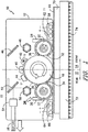
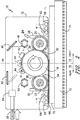
- FIGS. 1 and 2 show an exemplary embodiment of an additive manufacturing system 10, depicted as cross-section of a direct metal electrophotography machine (DME), for printing a three-dimensional part having a mobile housing 12 defining a front housing section 14 and rear housing section 16.
- DME direct metal electrophotography machine
- the exemplary additive manufacturing system 10 of FIGS. 1 and 2 includes a photoreceptor drum 18, having a drum outer surface 19, positioned within a mobile housing 12.
- a photoreceptor drum 18 is shown as being centrally disposed within the mobile housing 12, any suitable configuration can be utilized in accordance with the present description.
- the mobile housing 12 is positioned adjacent to a workpart 70, such that the drum outer surface 19 of the photoreceptor drum 18 is facing the printable surface 71 of the workpart 70.
- the workpart 70 is constructed from an electrically conducting material, such as a metal, so as to allow electrical biasing thereof.
- the workpart 70 can be constructed of a metal alloy, including superalloys of aluminum, iron, nickel, titanium, cobalt, chromium or mixtures thereof.
- a charging electrode 40 is positioned to apply electrostatic charge to the outer surface 19 of the photoreceptor drum 18 during an additive manufacturing process. Although shown as being centrally located within the housing 12 on the opposite side of the photoreceptor drum 18 from the workpart 70, the charging electrode 40 can be positioned in any suitable location within the housing 12 in accordance with the present disclosure. Generally, the charging electrode 40 projects an electrostatic charge onto the outer surface 19 of the photoreceptor drum 18 and/or any other revolving photosensitive drums or belts which are capable of holding an electrostatic charge on its surface. Thus, during printing, the outer surface 19 of the photoreceptor drum 18 is electrostatically charged after rotating by the charging electrode 40.
- the charging electrode 40 has a length that is at least as long as the length of the photoreceptor drum 18 so as to charge the entire outer surface 19 of the photoreceptor drum 18.
- the charging electrode 40 is a corona wire positioned parallel to the axis of the photoreceptor drum 18 to project an electrostatic charge thereon. It is noted that this process can be operated in the absence of light (i.e., without any lighting within the housing 12).
- An AC bias is also applied to the photoreceptor drum 18 to remove any residual charges left by previous layers.
- the photoreceptor drum 18 also has a DC bias, applied from the charging electrode 40, on the drum surface 19 to ensure a uniform negative potential thereon.
- the photoreceptor drum outer surface 19 can have a silicon coating with the photoconductive layer having three layers including, from the outermost inward, a Charge Transport Layer (CTL), Charge Generation Layer (CGL), and barrier or oxidizing layer formed on the underlying aluminum substrate.
- CTL Charge Transport Layer
- CGL Charge Generation Layer
- barrier or oxidizing layer formed on the underlying aluminum substrate.
- the CTL is a clear layer approximately 20 microns thick, which allows light to pass through to the CGL and controls charge acceptance to the photoreceptor drum outer surface 19.
- the CGL is about 0.1 to 1 micron thick and allows the flow of ions.
- the barrier layer bonds the photoconductive layer to the aluminum substrate.
- a laterally stationary platform 72 is disposed outside the mobile housing 12 adjacent the workpart 70, and can have at least one charged transfer electrode 74 in electrical communication with the laterally stationary platform 72.
- the photoreceptor drum 18 passes near the workpart 70, which is positively charged by transfer electrodes 74 on the back side of the platform 72, to pull the powder particles from the photoreceptor drum 18 to the workpart 70 and form a print layer 66, 68 according to the pattern on the outer surface 19.
- a controller circuit 56 performs multiple operations for the exemplary embodiment.
- the controller circuit 56 can provide motion commands for traversing the mobile housing 12 about the workpart 70 to position the DME 10 in accordance with a data stream from a print file (e.g., from a user's computer and/or other controller).
- the controller circuit 56 can also selectively reflect at least one laser diode 54 emission onto the photoreceptor drum 18 to expose a layer definition portion 51 of the outer surface 19 while the photoreceptor drum 18 rotates in opposing front and rear rotational directions.
- the laser diode(s) 54 can be directed to rotating polygonal scanning mirrors 48, 50, that direct the laser beam 55 through a system of lenses and mirrors onto the photoreceptor drum 18.
- a stream of model data from the controller circuit 56 turns the laser on and off to selectively irradiate the photoreceptor drum 18 surface 19 in those areas that do not correspond with the build layer cross section. Interaction of the laser 55 radiation with the photo reactive surface 19 enables local photoconductivity of the drum and permits surface static discharge of the areas where transfer of powder to the build layer is not desired. This process retains static charge of the drum surface 19 in those areas corresponding to the build cross section so that it may be subsequently used to lift and transfer powder to the drum surface 19 for application onto the workpart 70 as a build layer 68.
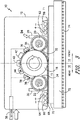
- exposure can also be performed using a front light emitting diode (LED) array 76 and rear light emitting diode (LED) array 78 spanning the width of the photoreceptor drum 18, each array being controlled by the controller circuit 56.
- LED light emitting diode
- LED rear light emitting diode
- the controller circuit 56 also simultaneously rotates a front charged powder roller 20 and a rear charged powder roller 22 in counter rotational directions, respectively synchronized with and counter to the front and rear rotational directions of the photoreceptor drum 18, thereby presenting a developed portion of charged powder onto the layer definition of the photoreceptor drum 18 and subsequently transferring the developed portion onto the workpart 70 as respective metal print layers 66, 68.
- the photoreceptor drum outer surface 19 with the layer definition is exposed to powder particles from the front and rear powder feed 28, 30 depending on the rotational direction of the photoreceptor drum 18.
- the powder particles are given a negative charge, and are electrostatically attracted to the photoreceptor drum layer definition, i.e. the areas touched by the laser. Because like charges repel, the negatively charged powder will not attach to the drum where the negative charge remains.
- the front and rear powder rollers 20, 22 can also apply a DC bias on the photoreceptor drum outer surface 19 to ensure a uniform negative potential.
- the front and rear powder cartridges 28, 30 can include metal materials, such as superalloys of aluminum, iron, nickel, titanium, cobalt, chromium or mixtures thereof, for formation and depositing of metal print layers 66, 68 of the same composition.
- the controller circuit 56 also can control fusing operations of front and rear microwave emitters 58, 60 disposed inside the mobile housing 12, for fusing the respective metal print layers 66, 68 to the workpart 70. Additionally, the controller circuit 56 can control operation of front and rear induction coils 62, 64 disposed inside the mobile housing, for heating the workpart using thermal radiation, though any suitable heat supply can be utilized. During forward direction motion (see Fig.
- front microwave emitters 58 and/or front induction coils 62 pre-heat the workpart 70 to prepare the surface for transferring the developed layer definition and acts to reduce the propensity of cracking and thermal distortion while rear microwave emitters 60 and/or rear induction coils 64 sinter the current developed layer definition to bind to the workpart 70.
- rearward direction motion see Fig. 1
- the front and rear microwave emitters 58, 60 can operate at frequencies of about 100 MHz to about 300 GHz, or any frequency suitable for coupling with the powder and/or workpart 70. That is, the microwave emitters 58, 60 can emit electromagnetic radiation having a wavelength of about 100 MHz to about 300 GHz.
- the controller circuit 56 may include suitable computer-readable instructions that, when implemented, configure the controller circuit 56 to perform various different functions, such as receiving, transmitting and/or executing control signals using computer logic.
- a computer generally includes a processor(s) and a memory.
- the processor(s) can be any known processing device.
- Memory can include any suitable computer-readable medium or media, including, but not limited to, RAM, ROM, hard drives, flash drives, or other memory devices.
- Memory stores information accessible by processor(s), including instructions that can be executed by processor(s).
- the instructions can be any set of instructions that when executed by the processor(s), cause the processor(s) to provide desired functionality.
- the instructions can be software instructions rendered in a computer-readable form. When software is used, any suitable programming, scripting, or other type of language or combinations of languages may be used to implement the teachings contained herein.
- the instructions can be implemented by hard-wired logic or other circuitry, including, but not limited to application-specific circuits.
- Memory can also include data that may be retrieved, manipulated, or stored by processor(s). For instance, after receiving the DME 10 layer definition, memory can store the information. Additionally, memory can store parameters for various other sources.
- the computing device can include a network interface for accessing information over a network.
- the network can include a combination of networks, such as Wi-Fi network, LAN, WAN, the Internet, cellular network, and/or other suitable network and can include any number of wired or wireless communication links.
- the computing device could communicate through a wired or wireless network with the DME 10.
- a cleaning operation of the DME 10 additive manufacturing system can include front and rear powder skimmers 36, 38 disposed adjacent the front and rear charged powder rollers 20, 22 for cleaning excess powder from the photoreceptor drum 18.
- the front and rear powder skimmers 36, 38 can also include front and rear adjustable layer cutting blades 32, 34.
- the electrically neutral adjustable layer cutting blades 32, 34 clean any excess powder from the photoreceptor drum 18 and deposits the powder back into the respective powder cartridge 28, 30.
- the laterally stationary platform 72 drops by the layer thickness blade setting on the adjustable layer cutting blades 32, 34 and the mobile print head housing 12 begins to traverse in the opposite direction for the next layer. This operation repeats until the workpart is complete.
- Additional structures in the DME 10 front housing section 14 can include at least one fixed mirror 46 and at least one front scanning mirror 48 for reflection of the laser beam, and at least one front discharge lamp 42 for discharging the photoreceptor drum outer surface 19.
- Additional structures in the DME 10 rear housing section 16 can include at least one side selector mirror 52 and at least one rear scanning mirror 50 for reflection of the laser beam, and at least one rear discharge lamp 44 for discharging the photoreceptor drum outer surface 19.
- the DME 10 additive manufacturing system is sizeable to any length without affecting functionality and multiple print heads can installed in a single mobile housing 12. Multiple mobile housings 12 can be used to build the same part on a single workpart 70.
- the DME 10 additive manufacturing system deposits directly onto the workpart only the quantity and layers of build material required to build the part, with minimal waste. That is, after printing utilizing the DME 10 additive manufacturing system, there is little-to-no excess powder to remove from the printed surface and very little post processing of the part.
- the DME 10 additive manufacturing system also reduces and/or eliminates thermal stresses through the process via layerwise heating, and prints in two dimensions (2-D linear fusing). Thus, there is no need for thermal cycles to relieve stress in the workpart following printing using the DME 10 additive manufacturing system.
- a method for printing a three-dimensional part involves charging an outer surface of a rotating photoreceptor drum with an electrostatic charge; neutralizing the electrostatic charge on a portion of the outer surface of the rotating photoreceptor drum surface to form a layer definition corresponding to the neutralized portion; then transferring a plurality of charged metal powder particles onto the outer surface of the rotating photoreceptor drum corresponding to the neutralized portion; and transferring the charged metal powder particles from the outer surface of the rotating photoreceptor drum onto a workpart to form a metal print layer.
- the method can use a metal workpart positioned on an electrically charged, stationary platform wherein the rotating photoreceptor drum rolls over the workpart to transfer the charged metal powder particles from the outer surface of the rotating photoreceptor drum onto the workpart. Additionally, the method can involve fusing the metal print layer to the workpart using electromagnetic radiation having wavelengths of about 100 MHz to about 300 GHz. The printing method can also preheat the workpart, using thermal radiation for example, prior to transferring the charged metal powder particles from the outer surface of the rotating photoreceptor drum onto the workpart.
- the printing method can neutralize the electrostatic charge by exposing the rotating photoreceptor drum outer surface to a layer definition using at least one laser beam.
- the layer definition can be provided by a controller circuit.
- the charged metal powder particles can then be delivered from at least one charged powder roller onto the outer surface of the photoreceptor drum.
- any excess powder can be cleaned from the outer surface of the photoreceptor drum using at least one electrically neutral adjustable powder skimmer blade, and then depositing the excess powder back into the at least one charged powder roller.
- any remaining charge can be discharged from the photoreceptor drum outer surface using at least one discharge lamp and then re-charge the outer surface of the photoreceptor drum.
- a method for printing a three-dimensional part which involves positioning a metal workpart on a stationary platform; electrically charging the platform; preheating the metal workpart; rolling a rotating photoreceptor drum across the preheated metal workpart to transfer a plurality of charged metal powder particles from an outer surface of the rotating photoreceptor drum onto an outer surface of the workpart to form a metal print layer; and fusing the metal print layer to the workpart.
- the metal print layer can be fused to the workpart using electromagnetic radiation having wavelengths of about 100 MHz to about 300 GHz and the workpart can be preheated using thermal radiation.
- this method can involve charging the outer surface of the rotating photoreceptor drum with an electrostatic charge; neutralizing the electrostatic charge on a portion of the outer surface of the rotating photoreceptor drum surface to form a layer definition corresponding to the neutralized portion; and developing the layer definition with charged metal powder particles such that the charged metal powder particles are positioned on the outer surface of the rotating photoreceptor drum corresponding to the neutralized portion.
- the electrostatic charge can be neutralized by exposing the rotating photoreceptor drum outer surface to a layer definition using at least one laser beam.
- the layer definition can be provided by a controller circuit.
- the charged metal powder particles can be delivered from at least one charged powder roller onto the outer surface of the photoreceptor drum. After delivering the charged metal powder particles to the outer surface of the photoreceptor drum, excess powder can be cleaned from the outer surface of the photoreceptor drum using at least one electrically neutral adjustable powder skimmer blade and then depositing the excess powder back into the at least one charged powder roller.
- the rotating photoreceptor drum is rolled across the preheated metal workpart in a first direction, then the rotating photoreceptor drum is rolled across the preheated metal workpart in a second direction to transfer a second plurality of charged metal powder particles from the outer surface of the rotating photoreceptor drum onto the outer surface of the workpart to form a second metal print layer, then the second metal print layer is fused onto the workpart.
Landscapes
- Engineering & Computer Science (AREA)
- Manufacturing & Machinery (AREA)
- Chemical & Material Sciences (AREA)
- Materials Engineering (AREA)
- Health & Medical Sciences (AREA)
- General Health & Medical Sciences (AREA)
- Toxicology (AREA)
- Physics & Mathematics (AREA)
- Plasma & Fusion (AREA)
- Life Sciences & Earth Sciences (AREA)
- Sustainable Development (AREA)
- Automation & Control Theory (AREA)
- Optics & Photonics (AREA)
- General Physics & Mathematics (AREA)
- Mechanical Engineering (AREA)
- Powder Metallurgy (AREA)
- Combination Of More Than One Step In Electrophotography (AREA)
- Discharging, Photosensitive Material Shape In Electrophotography (AREA)
Abstract
Description
- The present subject matter relates generally to additive manufacturing systems and methods for building three-dimensional (3D) parts. In particular, the present disclosure relates to systems and processes for building 3D parts with direct metal electrophotography-based systems (DME) and/or ionography-based systems using metallic build materials.
- Additive manufacturing systems are used to build 3D parts from digital representations of the 3D parts (e.g., AMF and STL format files) using one or more additive manufacturing techniques. Examples of commercially available additive manufacturing techniques include extrusion-based techniques, ink jetting, selective laser sintering, powder/binder jetting, electron-beam melting, direct metal laser melting (DMLM), and stereolithographic processes. For each of these techniques, the digital representation of the 3D part is initially sliced into multiple horizontal (X-Y) layers. For each sliced layer, a tool path is then generated, which provides instructions for the particular additive manufacturing system to form the given layer.
- Current powder bed DMLM machines are fraught with limitations, especially those preventing large-size scalable systems, the limitations including but not limited to speed, powder volume, trapped powder, and thermal stresses. Speed limitations include recoating and laser scan times that are too slow. Current processes are essentially 1-D (point melting) repeated in X-Y space and then repeated in Z space. Typical layers require 300 seconds of laser time followed by 10 seconds of recoat time. Powder volume limitations exist because every nook and cranny of the build cube must be filled with powder requiring large volumes of powder charges which must be dealt with during and after build. For large area builds, this powder charge could be thousands of pounds. Also, trapped powder limitations occur because closed volumes are impossible to build as the powder cannot be evacuated. The current requirement to evacuate powder also limits design freedom. And, current DMLM machines impose large thermal stresses on parts resulting from rapid build material solidification thereby creating geometrical distortions and sometimes cracking in the parent material. In addition, the entire platform must be stress relieved prior to cut-off which is difficult for large parts due to the heavy loads and size limitations of commonly accessible furnaces.
- In two-dimensional (2D) printing, electrophotography (i.e., xerography) is a popular technology for creating 2D images on planar substrates, such as printing paper. Electrophotography systems include a conductive support drum coated with a photoconductive material layer, where latent electrostatic images are formed by charging and then image-wise exposing the photoconductive layer by an optical source. The latent electrostatic images are then moved to a developing station where toner is applied to charged areas of the photoconductive insulator to form visible images. The formed toner images are then transferred to substrates (e.g., printing paper) and affixed to the substrates with heat or pressure.
- However, a need exists for improved printing techniques for 3D printing, particularly with metal build materials.
- Aspects and advantages of the invention will be set forth in part in the following description, or may be obvious from the description, or may be learned through practice of the invention.
- An additive manufacturing system is generally provided for printing a three-dimensional part. In one embodiment, the additive manufacturing system includes a mobile housing defining a front housing section and rear housing section; a photoreceptor drum defining a drum outer surface; a charging electrode positioned to apply electrostatic charge to the photoreceptor drum outer surface; a laterally stationary platform disposed outside the mobile housing adjacent the workpart, the laterally stationary platform comprising at least one charged transfer electrode; a controller circuit for traversing the mobile housing about the workpart while selectively applying at least one laser diode emission onto the photoreceptor drum to expose a layer definition on the photoreceptor drum outer surface, the controller circuit simultaneously rotating a front charged powder roller and a rear charged powder roller in counter rotational directions, respectively synchronized with and counter to the front and rear rotational directions of the photoreceptor drum, thereby presenting a developed portion of charged powder onto the layer definition of the photoreceptor drum and subsequently transferring said developed portion onto the workpart as respective metal print layers; front and rear microwave emitters disposed inside the mobile housing for fusing the respective metal print layers; and front and rear induction coils disposed inside the mobile housing for heating the workpart.
- These and other features, aspects and advantages of the present invention will become better understood with reference to the following description and appended claims. The accompanying drawings, which are incorporated in and constitute a part of this specification, illustrate embodiments of the invention and, together with the description, serve to explain the principles of the invention.
- A full and enabling disclosure of the present invention, including the best mode thereof, directed to one of ordinary skill in the art, is set forth in the specification, which makes reference to the appended figures, in which:
-
FIG. 1 is a schematic of a mirrored DME 3D printer as it moves in the rearward direction; -
FIG. 2 is a schematic of a mirrored DME 3D printer as it moves in the frontward direction; and -
FIG. 3 is a schematic of an LED array DME 3D printer using light emitting diode arrays. - Reference will now be made in detail to present embodiments of the invention, one or more examples of which are illustrated in the accompanying drawings. The detailed description uses numerical and letter designations to refer to features in the drawings. Like or similar designations in the drawings and description have been used to refer to like or similar parts of the invention.
- Referring to the drawings,
FIGS. 1 and2 show an exemplary embodiment of anadditive manufacturing system 10, depicted as cross-section of a direct metal electrophotography machine (DME), for printing a three-dimensional part having amobile housing 12 defining afront housing section 14 andrear housing section 16. - The exemplary
additive manufacturing system 10 ofFIGS. 1 and2 includes aphotoreceptor drum 18, having a drumouter surface 19, positioned within amobile housing 12. Although thephotoreceptor drum 18 is shown as being centrally disposed within themobile housing 12, any suitable configuration can be utilized in accordance with the present description. - The
mobile housing 12 is positioned adjacent to aworkpart 70, such that the drumouter surface 19 of thephotoreceptor drum 18 is facing theprintable surface 71 of theworkpart 70. Generally, theworkpart 70 is constructed from an electrically conducting material, such as a metal, so as to allow electrical biasing thereof. For example, theworkpart 70 can be constructed of a metal alloy, including superalloys of aluminum, iron, nickel, titanium, cobalt, chromium or mixtures thereof. - A
charging electrode 40 is positioned to apply electrostatic charge to theouter surface 19 of thephotoreceptor drum 18 during an additive manufacturing process. Although shown as being centrally located within thehousing 12 on the opposite side of thephotoreceptor drum 18 from theworkpart 70, thecharging electrode 40 can be positioned in any suitable location within thehousing 12 in accordance with the present disclosure. Generally, thecharging electrode 40 projects an electrostatic charge onto theouter surface 19 of thephotoreceptor drum 18 and/or any other revolving photosensitive drums or belts which are capable of holding an electrostatic charge on its surface. Thus, during printing, theouter surface 19 of thephotoreceptor drum 18 is electrostatically charged after rotating by thecharging electrode 40. Generally, thecharging electrode 40 has a length that is at least as long as the length of thephotoreceptor drum 18 so as to charge the entireouter surface 19 of thephotoreceptor drum 18. In one embodiment, thecharging electrode 40 is a corona wire positioned parallel to the axis of thephotoreceptor drum 18 to project an electrostatic charge thereon. It is noted that this process can be operated in the absence of light (i.e., without any lighting within the housing 12). - An AC bias is also applied to the
photoreceptor drum 18 to remove any residual charges left by previous layers. Thephotoreceptor drum 18 also has a DC bias, applied from thecharging electrode 40, on thedrum surface 19 to ensure a uniform negative potential thereon. - The photoreceptor drum
outer surface 19 can have a silicon coating with the photoconductive layer having three layers including, from the outermost inward, a Charge Transport Layer (CTL), Charge Generation Layer (CGL), and barrier or oxidizing layer formed on the underlying aluminum substrate. The CTL is a clear layer approximately 20 microns thick, which allows light to pass through to the CGL and controls charge acceptance to the photoreceptor drumouter surface 19. The CGL is about 0.1 to 1 micron thick and allows the flow of ions. The barrier layer bonds the photoconductive layer to the aluminum substrate. - A laterally
stationary platform 72 is disposed outside themobile housing 12 adjacent theworkpart 70, and can have at least one chargedtransfer electrode 74 in electrical communication with the laterallystationary platform 72. Thephotoreceptor drum 18 passes near theworkpart 70, which is positively charged bytransfer electrodes 74 on the back side of theplatform 72, to pull the powder particles from thephotoreceptor drum 18 to theworkpart 70 and form aprint layer outer surface 19. - A
controller circuit 56 performs multiple operations for the exemplary embodiment. Thecontroller circuit 56 can provide motion commands for traversing themobile housing 12 about theworkpart 70 to position theDME 10 in accordance with a data stream from a print file (e.g., from a user's computer and/or other controller). Thecontroller circuit 56 can also selectively reflect at least onelaser diode 54 emission onto thephotoreceptor drum 18 to expose alayer definition portion 51 of theouter surface 19 while thephotoreceptor drum 18 rotates in opposing front and rear rotational directions. The laser diode(s) 54 can be directed to rotatingpolygonal scanning mirrors laser beam 55 through a system of lenses and mirrors onto thephotoreceptor drum 18. Thephotoreceptor drum 18 continues to rotate during the sweep and the angle of sweep compensates for this motion. A stream of model data from thecontroller circuit 56 turns the laser on and off to selectively irradiate thephotoreceptor drum 18surface 19 in those areas that do not correspond with the build layer cross section. Interaction of thelaser 55 radiation with the photoreactive surface 19 enables local photoconductivity of the drum and permits surface static discharge of the areas where transfer of powder to the build layer is not desired. This process retains static charge of thedrum surface 19 in those areas corresponding to the build cross section so that it may be subsequently used to lift and transfer powder to thedrum surface 19 for application onto theworkpart 70 as abuild layer 68. - As shown in
FIG. 3 , exposure can also be performed using a front light emitting diode (LED)array 76 and rear light emitting diode (LED)array 78 spanning the width of thephotoreceptor drum 18, each array being controlled by thecontroller circuit 56. - The
controller circuit 56 also simultaneously rotates a front chargedpowder roller 20 and a rear chargedpowder roller 22 in counter rotational directions, respectively synchronized with and counter to the front and rear rotational directions of thephotoreceptor drum 18, thereby presenting a developed portion of charged powder onto the layer definition of thephotoreceptor drum 18 and subsequently transferring the developed portion onto theworkpart 70 as respective metal print layers 66, 68. The photoreceptor drumouter surface 19 with the layer definition is exposed to powder particles from the front andrear powder feed photoreceptor drum 18. The powder particles are given a negative charge, and are electrostatically attracted to the photoreceptor drum layer definition, i.e. the areas touched by the laser. Because like charges repel, the negatively charged powder will not attach to the drum where the negative charge remains. The front andrear powder rollers outer surface 19 to ensure a uniform negative potential. - The front and
rear powder cartridges - The
controller circuit 56 also can control fusing operations of front andrear microwave emitters mobile housing 12, for fusing the respective metal print layers 66, 68 to theworkpart 70. Additionally, thecontroller circuit 56 can control operation of front and rear induction coils 62, 64 disposed inside the mobile housing, for heating the workpart using thermal radiation, though any suitable heat supply can be utilized. During forward direction motion (seeFig. 2 ) of themobile housing 12,front microwave emitters 58 and/or front induction coils 62 pre-heat theworkpart 70 to prepare the surface for transferring the developed layer definition and acts to reduce the propensity of cracking and thermal distortion whilerear microwave emitters 60 and/or rear induction coils 64 sinter the current developed layer definition to bind to theworkpart 70. During rearward direction motion (seeFig. 1 ) of themobile housing 12, the front and rear fusing operations of the microwave emitters and induction coils are reversed. The front andrear microwave emitters workpart 70. That is, themicrowave emitters - The
controller circuit 56 may include suitable computer-readable instructions that, when implemented, configure thecontroller circuit 56 to perform various different functions, such as receiving, transmitting and/or executing control signals using computer logic. - A computer generally includes a processor(s) and a memory. The processor(s) can be any known processing device. Memory can include any suitable computer-readable medium or media, including, but not limited to, RAM, ROM, hard drives, flash drives, or other memory devices. Memory stores information accessible by processor(s), including instructions that can be executed by processor(s). The instructions can be any set of instructions that when executed by the processor(s), cause the processor(s) to provide desired functionality. For instance, the instructions can be software instructions rendered in a computer-readable form. When software is used, any suitable programming, scripting, or other type of language or combinations of languages may be used to implement the teachings contained herein. Alternatively, the instructions can be implemented by hard-wired logic or other circuitry, including, but not limited to application-specific circuits.
- Memory can also include data that may be retrieved, manipulated, or stored by processor(s). For instance, after receiving the
DME 10 layer definition, memory can store the information. Additionally, memory can store parameters for various other sources. - The computing device can include a network interface for accessing information over a network. The network can include a combination of networks, such as Wi-Fi network, LAN, WAN, the Internet, cellular network, and/or other suitable network and can include any number of wired or wireless communication links. For instance, the computing device could communicate through a wired or wireless network with the
DME 10. - A cleaning operation of the
DME 10 additive manufacturing system can include front andrear powder skimmers powder rollers photoreceptor drum 18. The front andrear powder skimmers layer cutting blades layer cutting blades photoreceptor drum 18 and deposits the powder back into therespective powder cartridge stationary platform 72 drops by the layer thickness blade setting on the adjustablelayer cutting blades print head housing 12 begins to traverse in the opposite direction for the next layer. This operation repeats until the workpart is complete. - Additional structures in the
DME 10front housing section 14 can include at least one fixedmirror 46 and at least onefront scanning mirror 48 for reflection of the laser beam, and at least onefront discharge lamp 42 for discharging the photoreceptor drumouter surface 19. Additional structures in theDME 10rear housing section 16 can include at least oneside selector mirror 52 and at least onerear scanning mirror 50 for reflection of the laser beam, and at least onerear discharge lamp 44 for discharging the photoreceptor drumouter surface 19. - The
DME 10 additive manufacturing system is sizeable to any length without affecting functionality and multiple print heads can installed in a singlemobile housing 12. Multiplemobile housings 12 can be used to build the same part on asingle workpart 70. - The
DME 10 additive manufacturing system deposits directly onto the workpart only the quantity and layers of build material required to build the part, with minimal waste. That is, after printing utilizing theDME 10 additive manufacturing system, there is little-to-no excess powder to remove from the printed surface and very little post processing of the part. - The
DME 10 additive manufacturing system also reduces and/or eliminates thermal stresses through the process via layerwise heating, and prints in two dimensions (2-D linear fusing). Thus, there is no need for thermal cycles to relieve stress in the workpart following printing using theDME 10 additive manufacturing system. - In one embodiment, a method for printing a three-dimensional part involves charging an outer surface of a rotating photoreceptor drum with an electrostatic charge; neutralizing the electrostatic charge on a portion of the outer surface of the rotating photoreceptor drum surface to form a layer definition corresponding to the neutralized portion; then transferring a plurality of charged metal powder particles onto the outer surface of the rotating photoreceptor drum corresponding to the neutralized portion; and transferring the charged metal powder particles from the outer surface of the rotating photoreceptor drum onto a workpart to form a metal print layer. The method can use a metal workpart positioned on an electrically charged, stationary platform wherein the rotating photoreceptor drum rolls over the workpart to transfer the charged metal powder particles from the outer surface of the rotating photoreceptor drum onto the workpart. Additionally, the method can involve fusing the metal print layer to the workpart using electromagnetic radiation having wavelengths of about 100 MHz to about 300 GHz. The printing method can also preheat the workpart, using thermal radiation for example, prior to transferring the charged metal powder particles from the outer surface of the rotating photoreceptor drum onto the workpart.
- In one embodiment, the printing method can neutralize the electrostatic charge by exposing the rotating photoreceptor drum outer surface to a layer definition using at least one laser beam. The layer definition can be provided by a controller circuit. The charged metal powder particles can then be delivered from at least one charged powder roller onto the outer surface of the photoreceptor drum. Then, after delivering the charged metal powder particles to the outer surface of the photoreceptor drum, any excess powder can be cleaned from the outer surface of the photoreceptor drum using at least one electrically neutral adjustable powder skimmer blade, and then depositing the excess powder back into the at least one charged powder roller. Then, any remaining charge can be discharged from the photoreceptor drum outer surface using at least one discharge lamp and then re-charge the outer surface of the photoreceptor drum.
- A method is also generally provided for printing a three-dimensional part, which involves positioning a metal workpart on a stationary platform; electrically charging the platform; preheating the metal workpart; rolling a rotating photoreceptor drum across the preheated metal workpart to transfer a plurality of charged metal powder particles from an outer surface of the rotating photoreceptor drum onto an outer surface of the workpart to form a metal print layer; and fusing the metal print layer to the workpart. In this method, the metal print layer can be fused to the workpart using electromagnetic radiation having wavelengths of about 100 MHz to about 300 GHz and the workpart can be preheated using thermal radiation. Additionally, this method can involve charging the outer surface of the rotating photoreceptor drum with an electrostatic charge; neutralizing the electrostatic charge on a portion of the outer surface of the rotating photoreceptor drum surface to form a layer definition corresponding to the neutralized portion; and developing the layer definition with charged metal powder particles such that the charged metal powder particles are positioned on the outer surface of the rotating photoreceptor drum corresponding to the neutralized portion. The electrostatic charge can be neutralized by exposing the rotating photoreceptor drum outer surface to a layer definition using at least one laser beam. The layer definition can be provided by a controller circuit.
- In one embodiment of the method, the charged metal powder particles can be delivered from at least one charged powder roller onto the outer surface of the photoreceptor drum. After delivering the charged metal powder particles to the outer surface of the photoreceptor drum, excess powder can be cleaned from the outer surface of the photoreceptor drum using at least one electrically neutral adjustable powder skimmer blade and then depositing the excess powder back into the at least one charged powder roller.
- In such an embodiment, the rotating photoreceptor drum is rolled across the preheated metal workpart in a first direction, then the rotating photoreceptor drum is rolled across the preheated metal workpart in a second direction to transfer a second plurality of charged metal powder particles from the outer surface of the rotating photoreceptor drum onto the outer surface of the workpart to form a second metal print layer, then the second metal print layer is fused onto the workpart.
- This written description uses examples to disclose the invention, including the best mode, and also to enable any person skilled in the art to practice the invention, including making and using any devices or systems and performing any incorporated methods. The patentable scope of the invention is defined by the claims, and may include other examples that occur to those skilled in the art. Such other examples are intended to be within the scope of the claims if they include structural elements that do not differ from the literal language of the claims, or if they include equivalent structural elements with insubstantial differences from the literal languages of the claims.
- Various aspects and embodiments of the present invention are defined by the following clauses:
- 1. An additive manufacturing system for printing a three-dimensional part, the additive manufacturing system comprising:
- a mobile housing defining a front housing section and rear housing section;
- a photoreceptor drum defining a drum outer surface;
- a charging electrode positioned to apply electrostatic charge to the photoreceptor drum outer surface;
- a laterally stationary platform disposed outside the mobile housing adjacent the workpart, the laterally stationary platform comprising at least one charged transfer electrode;
- a controller circuit for traversing the mobile housing about the workpart while selectively applying at least one laser diode emission onto the photoreceptor drum to expose a layer definition on the photoreceptor drum outer surface, the controller circuit simultaneously rotating a front charged powder roller and a rear charged powder roller in counter rotational directions, respectively synchronized with and counter to the front and rear rotational directions of the photoreceptor drum, thereby presenting a developed portion of charged powder onto the layer definition of the photoreceptor drum and subsequently transferring said developed portion onto the workpart as respective metal print layers;
- front and rear microwave emitters disposed inside the mobile housing for fusing the respective metal print layers; and
- front and rear induction coils disposed inside the mobile housing for heating the workpart.
- 2. The additive manufacturing system of clause 1, wherein the front housing section comprises a front powder skimmer disposed adjacent the front charged powder roller for cleaning excess powder.
- 3. The additive manufacturing system of clause 2, wherein the front powder skimmer comprises a front adjustable layer cutting blade.
- 4. The additive manufacturing system of clause 1, wherein the front housing section comprises at least one fixed mirror and at least one front scanning mirror.
- 5. The additive manufacturing system of clause 1, wherein the front housing section comprises at least one front discharge lamp for discharging the photoreceptor outer surface.
- 6. The additive manufacturing system of clause 1, wherein the rear housing section comprises a rear powder skimmer disposed adjacent the rear charged powder roller for cleaning excess powder.
- 7. The additive manufacturing system of clause 6, wherein the rear powder skimmer comprises a rear adjustable layer cutting blade.
- 8. The additive manufacturing system of clause 1, wherein the rear housing section comprises at least one side selector mirror and at least one rear scanning mirror.
- 9. The additive manufacturing system of clause 1, wherein the rear housing section comprises at least one rear discharge lamp for discharging the photoreceptor outer surface.
- 10. The additive manufacturing system of clause 1, wherein the front and rear microwave emitters operate at a frequency in the range of about 100 MHz to 100 GHz.
- 11. The additive manufacturing system of clause 1, wherein the metal print layers comprise superalloys of aluminum, iron, nickel, titanium, cobalt, chromium, or mixtures thereof.
- 12. An additive manufacturing system for printing a three-dimensional part, the additive manufacturing system comprising:
- a mobile housing defining a front housing section and rear housing section;
- a photoreceptor drum defining a drum outer surface, the photoreceptor drum centrally disposed in the mobile housing adjacent a workpart;
- a charging electrode centrally disposed in the mobile housing to apply electrostatic charge to the photoreceptor drum outer surface;
- a laterally stationary platform disposed outside the mobile housing adjacent the workpart, the laterally stationary platform comprising at least one charged transfer electrode;
- a controller circuit for traversing the mobile housing about the workpart while selectively energizing and directing at least one laser diode in a laser diode array onto the photoreceptor drum to expose a layer definition on the photoreceptor drum outer surface while the photoreceptor drum rotates in opposing front and
- rear rotational directions, the controller circuit simultaneously rotating a front charged powder roller and a rear charged powder roller in counter rotational directions, respectively, synchronized with and counter to the front and rear rotational directions of the photoreceptor drum, thereby producing a developed portion of charged powder onto the layer definition of the photoreceptor drum and subsequently transferring said developed portion onto the workpart as respective print layers;
- front and rear microwave emitters disposed inside the mobile housing for fusing the respective print layers, and
- front and rear induction coils disposed inside the mobile housing for heating the workpart.
- 13. The additive manufacturing system of
clause 12, wherein the front housing section comprises a front powder skimmer disposed adjacent the front charged powder roller for cleaning excess powder. - 14. The additive manufacturing system of clause 13, wherein the front powder skimmer comprises a front adjustable layer cutting blade.
- 15. The additive manufacturing system of
clause 12, wherein the front housing section comprises at least one front discharge lamp for discharging the photoreceptor outer surface. - 16. The additive manufacturing system of
clause 12, wherein the rear housing section comprises a rear powder skimmer disposed adjacent the rear charged powder roller for cleaning excess powder, said rear powder skimmer comprising a rear adjustable layer cutting blade. - 17. The additive manufacturing system of
clause 12, wherein the rear housing section comprises at least one rear discharge lamp for discharging the photoreceptor outer surface. - 18. The additive manufacturing system of
clause 12, wherein the front and rear microwave emitters operate at a frequency in the range of about 100 MHz to 100 GHz. - 19. The additive manufacturing system of
clause 12, wherein the metal print layers comprise superalloys of aluminum, iron, nickel, titanium, cobalt, chromium, or mixtures thereof.
Claims (10)
- An additive manufacturing system (10) for printing a three-dimensional part, the additive manufacturing system (10) comprising:a mobile housing (10) defining a front housing section (14) and rear housing section (16);a photoreceptor drum (18) defining a drum outer surface (19);a charging electrode (40) positioned to apply electrostatic charge to the photoreceptor drum outer surface (19);a laterally stationary platform (72) disposed outside the mobile housing (10) adjacent the workpart (70), the laterally stationary platform (72) comprising at least one charged transfer electrode (74);a controller circuit (56) for traversing the mobile housing (10) about the workpart (70) while selectively applying at least one laser diode (54) emission onto the photoreceptor drum (18) to expose a layer definition on the photoreceptor drum outer surface (19), the controller circuit (56) simultaneously rotating a front charged powder roller (20) and a rear charged powder roller (22) in counter rotational directions, respectively synchronized with and counter to the front and rear rotational directions of the photoreceptor drum (18), thereby presenting a developed portion of charged powder onto the layer definition of the photoreceptor drum (18) and subsequently transferring said developed portion onto the workpart (70) as respective metal print layers (66,68);front and rear microwave emitters (58,60) disposed inside the mobile housing (10) for fusing the respective metal print layers (66,68); andfront and rear induction coils (62,64) disposed inside the mobile housing (10) for heating the workpart (70).
- The additive manufacturing system (10) of claim 1, wherein the front housing section (14) comprises;
a front powder skimmer (36) disposed adjacent the front charged powder roller (20) for cleaning excess powder, wherein the front powder skimmer (36) comprises a front adjustable layer cutting blade (32), and
at least one fixed mirror (46), at least one front scanning mirror (48), and at least one front discharge lamp (42) for discharging the photoreceptor outer surface (19). - The additive manufacturing system (10) of claim 1, wherein the rear housing section (16) comprises;
a rear powder skimmer (22) disposed adjacent the rear charged powder roller (22) for cleaning excess powder, wherein the rear powder skimmer (22) comprises a rear adjustable layer cutting blade (34), and
at least one side selector mirror (52), at least one rear scanning mirror (50), and at least one rear discharge lamp (44) for discharging the photoreceptor outer surface (19). - The additive manufacturing system (10) of claim 1, wherein the front and rear microwave emitters (58,60) operate at a frequency in the range of about 100 MHz to 100 GHz.
- The additive manufacturing system (10) of claim 1, wherein the metal print layers (66,68) comprise superalloys of aluminum, iron, nickel, titanium, cobalt, chromium, or mixtures thereof.
- An additive manufacturing system (10) for printing a three-dimensional part, the additive manufacturing system (10) comprising:a mobile housing (12) defining a front housing section (14) and rear housing section (16);a photoreceptor drum (18) defining a drum outer surface (19), the photoreceptor drum (18) centrally disposed in the mobile housing (12) adjacent a workpart (70);a charging electrode (40) centrally disposed in the mobile housing (12) to apply electrostatic charge to the photoreceptor drum outer surface (19);a laterally stationary platform (72) disposed outside the mobile housing (12) adjacent the workpart (70), the laterally stationary platform (72) comprising at least one charged transfer electrode (74);a controller circuit (56) for traversing the mobile housing (12) about the workpart (70) while selectively energizing and directing at least one laser diode in a laser diode array (76,78) onto the photoreceptor drum (18) to expose a layer definition on the photoreceptor drum outer surface (19) while the photoreceptor drum (18) rotates in opposing front and rear rotational directions, the controller circuit (56) simultaneously rotating a front charged powder roller (20) and a rear charged powder roller (22) in counter rotational directions, respectively, synchronized with and counter to the front and rear rotational directions of the photoreceptor drum (18), thereby producing a developed portion of charged powder onto the layer definition of the photoreceptor drum (18) and subsequently transferring said developed portion onto the workpart (70) as respective print layers (66,68);front and rear microwave emitters (58,60) disposed inside the mobile housing (12) for fusing the respective print layers (66,68), andfront and rear induction coils (62,64) disposed inside the mobile housing (12) for heating the workpart (70).
- The additive manufacturing system (10) of claim 6, wherein the front housing section (14) comprises;
a front powder skimmer (36) disposed adjacent the front charged powder roller (20) for cleaning excess powder, wherein the front powder skimmer (36) comprises a front adjustable layer cutting blade (32), and
at least one front discharge lamp (42) for discharging the photoreceptor outer surface (19). - The additive manufacturing system (10) of claim 6, wherein the rear housing section (16) comprises;
a rear powder skimmer (38) disposed adjacent the rear charged powder roller (30) for cleaning excess powder, said rear powder skimmer (38) comprising a rear adjustable layer cutting blade (34), and
at least one rear discharge lamp (44) for discharging the photoreceptor outer surface (19). - The additive manufacturing system (10) of claim 6, wherein the front and rear microwave emitters (58,60) operate at a frequency in the range of about 100 MHz to 100 GHz.
- The additive manufacturing system (10) of claim 6, wherein the metal print layers (66,68) comprise superalloys of aluminum, iron, nickel, titanium, cobalt, chromium, or mixtures thereof.
Applications Claiming Priority (1)
| Application Number | Priority Date | Filing Date | Title |
|---|---|---|---|
| US14/956,942 US9566647B1 (en) | 2015-12-02 | 2015-12-02 | Direct metal electrophotography additive manufacturing machine |
Publications (2)
| Publication Number | Publication Date |
|---|---|
| EP3176647A1 true EP3176647A1 (en) | 2017-06-07 |
| EP3176647B1 EP3176647B1 (en) | 2018-10-03 |
Family
ID=57680047
Family Applications (1)
| Application Number | Title | Priority Date | Filing Date |
|---|---|---|---|
| EP16201014.4A Not-in-force EP3176647B1 (en) | 2015-12-02 | 2016-11-29 | Direct metal electrophotography additive manufacturing machine |
Country Status (6)
| Country | Link |
|---|---|
| US (1) | US9566647B1 (en) |
| EP (1) | EP3176647B1 (en) |
| JP (1) | JP6475685B2 (en) |
| CN (1) | CN106825562B (en) |
| BR (1) | BR102016028245A2 (en) |
| CA (1) | CA2949037C (en) |
Families Citing this family (7)
| Publication number | Priority date | Publication date | Assignee | Title |
|---|---|---|---|---|
| CN107708970A (en) | 2015-06-19 | 2018-02-16 | 应用材料公司 | Selective Powder Deposition in Additive Manufacturing |
| US10150255B2 (en) | 2015-12-02 | 2018-12-11 | General Electric Company | Direct metal electrophotography additive manufacturing methods |
| CN106825571B (en) * | 2017-03-31 | 2018-03-23 | 杨沛恩 | A kind of coaxial powder feeding apparatus for 3D printing metal works |
| CN107052339A (en) * | 2017-03-31 | 2017-08-18 | 杨沛恩 | A kind of coaxial powder feeding apparatus for 3D printing metal works |
| US10682703B2 (en) * | 2017-11-07 | 2020-06-16 | Aaron Roni Shafir | Systems and methods for delivering materials for printing three dimensional (3D) objects |
| CN117259785B (en) * | 2023-10-20 | 2025-11-04 | 浙江工业大学 | Methods and systems for SLM additive manufacturing of homogeneous materials |
| CN119217719B (en) * | 2024-11-28 | 2025-02-25 | 江苏微众快速制造科技有限公司 | Machining system for 3D printing of engine blisk |
Citations (3)
| Publication number | Priority date | Publication date | Assignee | Title |
|---|---|---|---|---|
| WO2007073205A1 (en) * | 2005-12-20 | 2007-06-28 | Sinvent As | Method and apparatus for consolidation in layers |
| US20130077996A1 (en) * | 2011-09-23 | 2013-03-28 | Stratasys, Inc. | Electrophotography-based additive manufacturing system with reciprocating operation |
| WO2015091826A1 (en) * | 2013-12-20 | 2015-06-25 | Dominique Paetz | Additive manufacturing apparatus and method for operating the same |
Family Cites Families (12)
| Publication number | Priority date | Publication date | Assignee | Title |
|---|---|---|---|---|
| JPS54144203A (en) | 1978-05-01 | 1979-11-10 | Fuji Yakuhin Kogyo Kk | Method of making flat printing plate |
| JP4324120B2 (en) | 2005-02-18 | 2009-09-02 | キヤノン株式会社 | Magnetic toner |
| JP2013076997A (en) | 2011-09-15 | 2013-04-25 | Ricoh Co Ltd | Toner for electrophotographic image formation, production method of toner for electrophotographic image formation, image forming method, and process cartridge |
| US8488994B2 (en) | 2011-09-23 | 2013-07-16 | Stratasys, Inc. | Electrophotography-based additive manufacturing system with transfer-medium service loops |
| CN104057083B (en) * | 2013-03-22 | 2016-02-24 | 通用电气公司 | For the manufacture of the method for part taking high melting point metal materials as base material |
| US9144940B2 (en) | 2013-07-17 | 2015-09-29 | Stratasys, Inc. | Method for printing 3D parts and support structures with electrophotography-based additive manufacturing |
| US9029058B2 (en) | 2013-07-17 | 2015-05-12 | Stratasys, Inc. | Soluble support material for electrophotography-based additive manufacturing |
| KR101774462B1 (en) | 2013-07-17 | 2017-09-04 | 스트래터시스,인코포레이티드 | Semi-crystalline consumable materials for electrophotography-based additive manufacturing system |
| US9523934B2 (en) | 2013-07-17 | 2016-12-20 | Stratasys, Inc. | Engineering-grade consumable materials for electrophotography-based additive manufacturing |
| US20150024317A1 (en) | 2013-07-17 | 2015-01-22 | Stratasys, Inc. | High-Performance Consumable Materials for Electrophotography-Based Additive Manufacturing |
| US9023566B2 (en) | 2013-07-17 | 2015-05-05 | Stratasys, Inc. | ABS part material for electrophotography-based additive manufacturing |
| US20150273582A1 (en) * | 2014-04-01 | 2015-10-01 | Stratasys, Inc. | System and Method for Printing Three-Dimensional Parts with Magnetic Support Media |
-
2015
- 2015-12-02 US US14/956,942 patent/US9566647B1/en not_active Expired - Fee Related
-
2016
- 2016-11-17 CA CA2949037A patent/CA2949037C/en active Active
- 2016-11-24 JP JP2016227401A patent/JP6475685B2/en not_active Expired - Fee Related
- 2016-11-29 EP EP16201014.4A patent/EP3176647B1/en not_active Not-in-force
- 2016-12-01 BR BR102016028245A patent/BR102016028245A2/en not_active Application Discontinuation
- 2016-12-02 CN CN201611095656.1A patent/CN106825562B/en not_active Expired - Fee Related
Patent Citations (3)
| Publication number | Priority date | Publication date | Assignee | Title |
|---|---|---|---|---|
| WO2007073205A1 (en) * | 2005-12-20 | 2007-06-28 | Sinvent As | Method and apparatus for consolidation in layers |
| US20130077996A1 (en) * | 2011-09-23 | 2013-03-28 | Stratasys, Inc. | Electrophotography-based additive manufacturing system with reciprocating operation |
| WO2015091826A1 (en) * | 2013-12-20 | 2015-06-25 | Dominique Paetz | Additive manufacturing apparatus and method for operating the same |
Also Published As
| Publication number | Publication date |
|---|---|
| US9566647B1 (en) | 2017-02-14 |
| JP6475685B2 (en) | 2019-02-27 |
| CN106825562A (en) | 2017-06-13 |
| JP2017115237A (en) | 2017-06-29 |
| CA2949037A1 (en) | 2017-06-02 |
| EP3176647B1 (en) | 2018-10-03 |
| CA2949037C (en) | 2019-03-19 |
| CN106825562B (en) | 2019-11-19 |
| BR102016028245A2 (en) | 2017-06-06 |
Similar Documents
| Publication | Publication Date | Title |
|---|---|---|
| EP3176648B1 (en) | Direct metal electrophotography additive manufacturing methods | |
| EP3176647B1 (en) | Direct metal electrophotography additive manufacturing machine | |
| US10105902B2 (en) | Electrophotography-based additive manufacturing with part molding | |
| EP1735133B1 (en) | Apparatus and method for three dimensional printing using imaged layers | |
| US8879957B2 (en) | Electrophotography-based additive manufacturing system with reciprocating operation | |
| US11590695B2 (en) | Photocuring printing system and method | |
| CA3009454A1 (en) | Building with cylindrical layers in additive manufacturing | |
| US20170291362A1 (en) | Printing 3d parts with controlled surface finish | |
| WO2011065920A1 (en) | Process for building three-dimensional objects | |
| US10112379B2 (en) | Large format electrophotographic 3D printer | |
| US9308691B2 (en) | Device and method for producing a three dimensional object | |
| US20190204769A1 (en) | Height control in selective deposition based additive manufacturing of parts | |
| US20220227040A1 (en) | Selective deposition-based additive manufacturing device and method of printing 3d parts with semi-crystalline materials | |
| EP3993988A1 (en) | Selective layer deposition based additive manufacturing system using laser nip heating | |
| US20250065559A1 (en) | Additive manufacturing system and method with smooth surface | |
| US11161309B2 (en) | Electrophotography-based 3D printing with improved layer uniformity | |
| US11203150B2 (en) | Layer orientation in selective deposition based additive manufacturing of parts | |
| WO2023192591A1 (en) | Additive manufacturing materials and methods with improved color |
Legal Events
| Date | Code | Title | Description |
|---|---|---|---|
| AK | Designated contracting states |
Kind code of ref document: A1 Designated state(s): AL AT BE BG CH CY CZ DE DK EE ES FI FR GB GR HR HU IE IS IT LI LT LU LV MC MK MT NL NO PL PT RO RS SE SI SK SM TR |
|
| AX | Request for extension of the european patent |
Extension state: BA ME |
|
| PUAI | Public reference made under article 153(3) epc to a published international application that has entered the european phase |
Free format text: ORIGINAL CODE: 0009012 |
|
| 17P | Request for examination filed |
Effective date: 20171207 |
|
| RBV | Designated contracting states (corrected) |
Designated state(s): AL AT BE BG CH CY CZ DE DK EE ES FI FR GB GR HR HU IE IS IT LI LT LU LV MC MK MT NL NO PL PT RO RS SE SI SK SM TR |
|
| GRAP | Despatch of communication of intention to grant a patent |
Free format text: ORIGINAL CODE: EPIDOSNIGR1 |
|
| INTG | Intention to grant announced |
Effective date: 20180504 |
|
| GRAS | Grant fee paid |
Free format text: ORIGINAL CODE: EPIDOSNIGR3 |
|
| GRAA | (expected) grant |
Free format text: ORIGINAL CODE: 0009210 |
|
| AK | Designated contracting states |
Kind code of ref document: B1 Designated state(s): AL AT BE BG CH CY CZ DE DK EE ES FI FR GB GR HR HU IE IS IT LI LT LU LV MC MK MT NL NO PL PT RO RS SE SI SK SM TR |
|
| REG | Reference to a national code |
Ref country code: GB Ref legal event code: FG4D |
|
| REG | Reference to a national code |
Ref country code: CH Ref legal event code: EP Ref country code: AT Ref legal event code: REF Ref document number: 1049269 Country of ref document: AT Kind code of ref document: T Effective date: 20181015 |
|
| REG | Reference to a national code |
Ref country code: IE Ref legal event code: FG4D Ref country code: DE Ref legal event code: R096 Ref document number: 602016006210 Country of ref document: DE |
|
| REG | Reference to a national code |
Ref country code: NL Ref legal event code: MP Effective date: 20181003 |
|
| REG | Reference to a national code |
Ref country code: LT Ref legal event code: MG4D |
|
| REG | Reference to a national code |
Ref country code: AT Ref legal event code: MK05 Ref document number: 1049269 Country of ref document: AT Kind code of ref document: T Effective date: 20181003 |
|
| PG25 | Lapsed in a contracting state [announced via postgrant information from national office to epo] |
Ref country code: NL Free format text: LAPSE BECAUSE OF FAILURE TO SUBMIT A TRANSLATION OF THE DESCRIPTION OR TO PAY THE FEE WITHIN THE PRESCRIBED TIME-LIMIT Effective date: 20181003 |
|
| PG25 | Lapsed in a contracting state [announced via postgrant information from national office to epo] |
Ref country code: ES Free format text: LAPSE BECAUSE OF FAILURE TO SUBMIT A TRANSLATION OF THE DESCRIPTION OR TO PAY THE FEE WITHIN THE PRESCRIBED TIME-LIMIT Effective date: 20181003 Ref country code: CZ Free format text: LAPSE BECAUSE OF FAILURE TO SUBMIT A TRANSLATION OF THE DESCRIPTION OR TO PAY THE FEE WITHIN THE PRESCRIBED TIME-LIMIT Effective date: 20181003 Ref country code: LT Free format text: LAPSE BECAUSE OF FAILURE TO SUBMIT A TRANSLATION OF THE DESCRIPTION OR TO PAY THE FEE WITHIN THE PRESCRIBED TIME-LIMIT Effective date: 20181003 Ref country code: AT Free format text: LAPSE BECAUSE OF FAILURE TO SUBMIT A TRANSLATION OF THE DESCRIPTION OR TO PAY THE FEE WITHIN THE PRESCRIBED TIME-LIMIT Effective date: 20181003 Ref country code: IS Free format text: LAPSE BECAUSE OF FAILURE TO SUBMIT A TRANSLATION OF THE DESCRIPTION OR TO PAY THE FEE WITHIN THE PRESCRIBED TIME-LIMIT Effective date: 20190203 Ref country code: NO Free format text: LAPSE BECAUSE OF FAILURE TO SUBMIT A TRANSLATION OF THE DESCRIPTION OR TO PAY THE FEE WITHIN THE PRESCRIBED TIME-LIMIT Effective date: 20190103 Ref country code: FI Free format text: LAPSE BECAUSE OF FAILURE TO SUBMIT A TRANSLATION OF THE DESCRIPTION OR TO PAY THE FEE WITHIN THE PRESCRIBED TIME-LIMIT Effective date: 20181003 Ref country code: PL Free format text: LAPSE BECAUSE OF FAILURE TO SUBMIT A TRANSLATION OF THE DESCRIPTION OR TO PAY THE FEE WITHIN THE PRESCRIBED TIME-LIMIT Effective date: 20181003 Ref country code: BG Free format text: LAPSE BECAUSE OF FAILURE TO SUBMIT A TRANSLATION OF THE DESCRIPTION OR TO PAY THE FEE WITHIN THE PRESCRIBED TIME-LIMIT Effective date: 20190103 Ref country code: HR Free format text: LAPSE BECAUSE OF FAILURE TO SUBMIT A TRANSLATION OF THE DESCRIPTION OR TO PAY THE FEE WITHIN THE PRESCRIBED TIME-LIMIT Effective date: 20181003 Ref country code: LV Free format text: LAPSE BECAUSE OF FAILURE TO SUBMIT A TRANSLATION OF THE DESCRIPTION OR TO PAY THE FEE WITHIN THE PRESCRIBED TIME-LIMIT Effective date: 20181003 |
|
| PG25 | Lapsed in a contracting state [announced via postgrant information from national office to epo] |
Ref country code: RS Free format text: LAPSE BECAUSE OF FAILURE TO SUBMIT A TRANSLATION OF THE DESCRIPTION OR TO PAY THE FEE WITHIN THE PRESCRIBED TIME-LIMIT Effective date: 20181003 Ref country code: AL Free format text: LAPSE BECAUSE OF FAILURE TO SUBMIT A TRANSLATION OF THE DESCRIPTION OR TO PAY THE FEE WITHIN THE PRESCRIBED TIME-LIMIT Effective date: 20181003 Ref country code: SE Free format text: LAPSE BECAUSE OF FAILURE TO SUBMIT A TRANSLATION OF THE DESCRIPTION OR TO PAY THE FEE WITHIN THE PRESCRIBED TIME-LIMIT Effective date: 20181003 Ref country code: PT Free format text: LAPSE BECAUSE OF FAILURE TO SUBMIT A TRANSLATION OF THE DESCRIPTION OR TO PAY THE FEE WITHIN THE PRESCRIBED TIME-LIMIT Effective date: 20190203 Ref country code: GR Free format text: LAPSE BECAUSE OF FAILURE TO SUBMIT A TRANSLATION OF THE DESCRIPTION OR TO PAY THE FEE WITHIN THE PRESCRIBED TIME-LIMIT Effective date: 20190104 |
|
| REG | Reference to a national code |
Ref country code: DE Ref legal event code: R097 Ref document number: 602016006210 Country of ref document: DE |
|
| PG25 | Lapsed in a contracting state [announced via postgrant information from national office to epo] |
Ref country code: DK Free format text: LAPSE BECAUSE OF FAILURE TO SUBMIT A TRANSLATION OF THE DESCRIPTION OR TO PAY THE FEE WITHIN THE PRESCRIBED TIME-LIMIT Effective date: 20181003 Ref country code: IT Free format text: LAPSE BECAUSE OF FAILURE TO SUBMIT A TRANSLATION OF THE DESCRIPTION OR TO PAY THE FEE WITHIN THE PRESCRIBED TIME-LIMIT Effective date: 20181003 Ref country code: LU Free format text: LAPSE BECAUSE OF NON-PAYMENT OF DUE FEES Effective date: 20181129 |
|
| PLBE | No opposition filed within time limit |
Free format text: ORIGINAL CODE: 0009261 |
|
| STAA | Information on the status of an ep patent application or granted ep patent |
Free format text: STATUS: NO OPPOSITION FILED WITHIN TIME LIMIT |
|
| REG | Reference to a national code |
Ref country code: BE Ref legal event code: MM Effective date: 20181130 |
|
| REG | Reference to a national code |
Ref country code: IE Ref legal event code: MM4A |
|
| PG25 | Lapsed in a contracting state [announced via postgrant information from national office to epo] |
Ref country code: SK Free format text: LAPSE BECAUSE OF FAILURE TO SUBMIT A TRANSLATION OF THE DESCRIPTION OR TO PAY THE FEE WITHIN THE PRESCRIBED TIME-LIMIT Effective date: 20181003 Ref country code: SM Free format text: LAPSE BECAUSE OF FAILURE TO SUBMIT A TRANSLATION OF THE DESCRIPTION OR TO PAY THE FEE WITHIN THE PRESCRIBED TIME-LIMIT Effective date: 20181003 Ref country code: EE Free format text: LAPSE BECAUSE OF FAILURE TO SUBMIT A TRANSLATION OF THE DESCRIPTION OR TO PAY THE FEE WITHIN THE PRESCRIBED TIME-LIMIT Effective date: 20181003 Ref country code: RO Free format text: LAPSE BECAUSE OF FAILURE TO SUBMIT A TRANSLATION OF THE DESCRIPTION OR TO PAY THE FEE WITHIN THE PRESCRIBED TIME-LIMIT Effective date: 20181003 Ref country code: MC Free format text: LAPSE BECAUSE OF FAILURE TO SUBMIT A TRANSLATION OF THE DESCRIPTION OR TO PAY THE FEE WITHIN THE PRESCRIBED TIME-LIMIT Effective date: 20181003 |
|
| 26N | No opposition filed |
Effective date: 20190704 |
|
| PG25 | Lapsed in a contracting state [announced via postgrant information from national office to epo] |
Ref country code: SI Free format text: LAPSE BECAUSE OF FAILURE TO SUBMIT A TRANSLATION OF THE DESCRIPTION OR TO PAY THE FEE WITHIN THE PRESCRIBED TIME-LIMIT Effective date: 20181003 Ref country code: IE Free format text: LAPSE BECAUSE OF NON-PAYMENT OF DUE FEES Effective date: 20181129 |
|
| PG25 | Lapsed in a contracting state [announced via postgrant information from national office to epo] |
Ref country code: BE Free format text: LAPSE BECAUSE OF NON-PAYMENT OF DUE FEES Effective date: 20181130 |
|
| PG25 | Lapsed in a contracting state [announced via postgrant information from national office to epo] |
Ref country code: MT Free format text: LAPSE BECAUSE OF NON-PAYMENT OF DUE FEES Effective date: 20181129 |
|
| PG25 | Lapsed in a contracting state [announced via postgrant information from national office to epo] |
Ref country code: TR Free format text: LAPSE BECAUSE OF FAILURE TO SUBMIT A TRANSLATION OF THE DESCRIPTION OR TO PAY THE FEE WITHIN THE PRESCRIBED TIME-LIMIT Effective date: 20181003 |
|
| PG25 | Lapsed in a contracting state [announced via postgrant information from national office to epo] |
Ref country code: HU Free format text: LAPSE BECAUSE OF FAILURE TO SUBMIT A TRANSLATION OF THE DESCRIPTION OR TO PAY THE FEE WITHIN THE PRESCRIBED TIME-LIMIT; INVALID AB INITIO Effective date: 20161129 Ref country code: MK Free format text: LAPSE BECAUSE OF NON-PAYMENT OF DUE FEES Effective date: 20181003 Ref country code: CY Free format text: LAPSE BECAUSE OF FAILURE TO SUBMIT A TRANSLATION OF THE DESCRIPTION OR TO PAY THE FEE WITHIN THE PRESCRIBED TIME-LIMIT Effective date: 20181003 |
|
| REG | Reference to a national code |
Ref country code: CH Ref legal event code: PL |
|
| PG25 | Lapsed in a contracting state [announced via postgrant information from national office to epo] |
Ref country code: CH Free format text: LAPSE BECAUSE OF NON-PAYMENT OF DUE FEES Effective date: 20191130 Ref country code: LI Free format text: LAPSE BECAUSE OF NON-PAYMENT OF DUE FEES Effective date: 20191130 |
|
| PGFP | Annual fee paid to national office [announced via postgrant information from national office to epo] |
Ref country code: FR Payment date: 20221021 Year of fee payment: 7 |
|
| PGFP | Annual fee paid to national office [announced via postgrant information from national office to epo] |
Ref country code: GB Payment date: 20221021 Year of fee payment: 7 Ref country code: DE Payment date: 20220616 Year of fee payment: 7 |
|
| REG | Reference to a national code |
Ref country code: GB Ref legal event code: 732E Free format text: REGISTERED BETWEEN 20231102 AND 20231108 |
|
| REG | Reference to a national code |
Ref country code: DE Ref legal event code: R082 Ref document number: 602016006210 Country of ref document: DE Ref country code: DE Ref legal event code: R081 Ref document number: 602016006210 Country of ref document: DE Owner name: GENERAL ELECTRIC RENOVABLES ESPANA, S.L., ES Free format text: FORMER OWNER: GENERAL ELECTRIC COMPANY, SCHENECTADY, NY, US |
|
| REG | Reference to a national code |
Ref country code: DE Ref legal event code: R119 Ref document number: 602016006210 Country of ref document: DE |
|
| GBPC | Gb: european patent ceased through non-payment of renewal fee |
Effective date: 20231129 |
|
| PG25 | Lapsed in a contracting state [announced via postgrant information from national office to epo] |
Ref country code: DE Free format text: LAPSE BECAUSE OF NON-PAYMENT OF DUE FEES Effective date: 20240601 |
|
| PG25 | Lapsed in a contracting state [announced via postgrant information from national office to epo] |
Ref country code: GB Free format text: LAPSE BECAUSE OF NON-PAYMENT OF DUE FEES Effective date: 20231129 |
|
| PG25 | Lapsed in a contracting state [announced via postgrant information from national office to epo] |
Ref country code: FR Free format text: LAPSE BECAUSE OF NON-PAYMENT OF DUE FEES Effective date: 20231130 |
|
| PG25 | Lapsed in a contracting state [announced via postgrant information from national office to epo] |
Ref country code: GB Free format text: LAPSE BECAUSE OF NON-PAYMENT OF DUE FEES Effective date: 20231129 Ref country code: FR Free format text: LAPSE BECAUSE OF NON-PAYMENT OF DUE FEES Effective date: 20231130 Ref country code: DE Free format text: LAPSE BECAUSE OF NON-PAYMENT OF DUE FEES Effective date: 20240601 |