EP3175989A1 - Ink jet head and printer - Google Patents
Ink jet head and printer Download PDFInfo
- Publication number
- EP3175989A1 EP3175989A1 EP15827276.5A EP15827276A EP3175989A1 EP 3175989 A1 EP3175989 A1 EP 3175989A1 EP 15827276 A EP15827276 A EP 15827276A EP 3175989 A1 EP3175989 A1 EP 3175989A1
- Authority
- EP
- European Patent Office
- Prior art keywords
- actuator substrate
- piezoelectric actuator
- printed circuit
- flexible printed
- inkjet head
- Prior art date
- Legal status (The legal status is an assumption and is not a legal conclusion. Google has not performed a legal analysis and makes no representation as to the accuracy of the status listed.)
- Granted
Links
Images





Classifications
-
- B—PERFORMING OPERATIONS; TRANSPORTING
- B41—PRINTING; LINING MACHINES; TYPEWRITERS; STAMPS
- B41J—TYPEWRITERS; SELECTIVE PRINTING MECHANISMS, i.e. MECHANISMS PRINTING OTHERWISE THAN FROM A FORME; CORRECTION OF TYPOGRAPHICAL ERRORS
- B41J2/00—Typewriters or selective printing mechanisms characterised by the printing or marking process for which they are designed
- B41J2/005—Typewriters or selective printing mechanisms characterised by the printing or marking process for which they are designed characterised by bringing liquid or particles selectively into contact with a printing material
- B41J2/01—Ink jet
- B41J2/135—Nozzles
- B41J2/14—Structure thereof only for on-demand ink jet heads
- B41J2/14201—Structure of print heads with piezoelectric elements
- B41J2/14233—Structure of print heads with piezoelectric elements of film type, deformed by bending and disposed on a diaphragm
-
- B—PERFORMING OPERATIONS; TRANSPORTING
- B41—PRINTING; LINING MACHINES; TYPEWRITERS; STAMPS
- B41J—TYPEWRITERS; SELECTIVE PRINTING MECHANISMS, i.e. MECHANISMS PRINTING OTHERWISE THAN FROM A FORME; CORRECTION OF TYPOGRAPHICAL ERRORS
- B41J2/00—Typewriters or selective printing mechanisms characterised by the printing or marking process for which they are designed
- B41J2/005—Typewriters or selective printing mechanisms characterised by the printing or marking process for which they are designed characterised by bringing liquid or particles selectively into contact with a printing material
- B41J2/01—Ink jet
- B41J2/015—Ink jet characterised by the jet generation process
- B41J2/04—Ink jet characterised by the jet generation process generating single droplets or particles on demand
- B41J2/045—Ink jet characterised by the jet generation process generating single droplets or particles on demand by pressure, e.g. electromechanical transducers
- B41J2/04501—Control methods or devices therefor, e.g. driver circuits, control circuits
- B41J2/04533—Control methods or devices therefor, e.g. driver circuits, control circuits controlling a head having several actuators per chamber
-
- B—PERFORMING OPERATIONS; TRANSPORTING
- B41—PRINTING; LINING MACHINES; TYPEWRITERS; STAMPS
- B41J—TYPEWRITERS; SELECTIVE PRINTING MECHANISMS, i.e. MECHANISMS PRINTING OTHERWISE THAN FROM A FORME; CORRECTION OF TYPOGRAPHICAL ERRORS
- B41J2/00—Typewriters or selective printing mechanisms characterised by the printing or marking process for which they are designed
- B41J2/005—Typewriters or selective printing mechanisms characterised by the printing or marking process for which they are designed characterised by bringing liquid or particles selectively into contact with a printing material
- B41J2/01—Ink jet
- B41J2/135—Nozzles
- B41J2/14—Structure thereof only for on-demand ink jet heads
- B41J2/14201—Structure of print heads with piezoelectric elements
- B41J2/14209—Structure of print heads with piezoelectric elements of finger type, chamber walls consisting integrally of piezoelectric material
-
- B—PERFORMING OPERATIONS; TRANSPORTING
- B41—PRINTING; LINING MACHINES; TYPEWRITERS; STAMPS
- B41J—TYPEWRITERS; SELECTIVE PRINTING MECHANISMS, i.e. MECHANISMS PRINTING OTHERWISE THAN FROM A FORME; CORRECTION OF TYPOGRAPHICAL ERRORS
- B41J2/00—Typewriters or selective printing mechanisms characterised by the printing or marking process for which they are designed
- B41J2/005—Typewriters or selective printing mechanisms characterised by the printing or marking process for which they are designed characterised by bringing liquid or particles selectively into contact with a printing material
- B41J2/01—Ink jet
- B41J2/135—Nozzles
- B41J2/16—Production of nozzles
- B41J2/1607—Production of print heads with piezoelectric elements
- B41J2/161—Production of print heads with piezoelectric elements of film type, deformed by bending and disposed on a diaphragm
-
- B—PERFORMING OPERATIONS; TRANSPORTING
- B41—PRINTING; LINING MACHINES; TYPEWRITERS; STAMPS
- B41J—TYPEWRITERS; SELECTIVE PRINTING MECHANISMS, i.e. MECHANISMS PRINTING OTHERWISE THAN FROM A FORME; CORRECTION OF TYPOGRAPHICAL ERRORS
- B41J2/00—Typewriters or selective printing mechanisms characterised by the printing or marking process for which they are designed
- B41J2/005—Typewriters or selective printing mechanisms characterised by the printing or marking process for which they are designed characterised by bringing liquid or particles selectively into contact with a printing material
- B41J2/01—Ink jet
- B41J2/135—Nozzles
- B41J2/16—Production of nozzles
- B41J2/1621—Manufacturing processes
- B41J2/1623—Manufacturing processes bonding and adhesion
-
- B—PERFORMING OPERATIONS; TRANSPORTING
- B41—PRINTING; LINING MACHINES; TYPEWRITERS; STAMPS
- B41J—TYPEWRITERS; SELECTIVE PRINTING MECHANISMS, i.e. MECHANISMS PRINTING OTHERWISE THAN FROM A FORME; CORRECTION OF TYPOGRAPHICAL ERRORS
- B41J2/00—Typewriters or selective printing mechanisms characterised by the printing or marking process for which they are designed
- B41J2/005—Typewriters or selective printing mechanisms characterised by the printing or marking process for which they are designed characterised by bringing liquid or particles selectively into contact with a printing material
- B41J2/01—Ink jet
- B41J2/135—Nozzles
- B41J2/16—Production of nozzles
- B41J2/1621—Manufacturing processes
- B41J2/1626—Manufacturing processes etching
-
- B—PERFORMING OPERATIONS; TRANSPORTING
- B41—PRINTING; LINING MACHINES; TYPEWRITERS; STAMPS
- B41J—TYPEWRITERS; SELECTIVE PRINTING MECHANISMS, i.e. MECHANISMS PRINTING OTHERWISE THAN FROM A FORME; CORRECTION OF TYPOGRAPHICAL ERRORS
- B41J2/00—Typewriters or selective printing mechanisms characterised by the printing or marking process for which they are designed
- B41J2/005—Typewriters or selective printing mechanisms characterised by the printing or marking process for which they are designed characterised by bringing liquid or particles selectively into contact with a printing material
- B41J2/01—Ink jet
- B41J2/135—Nozzles
- B41J2/16—Production of nozzles
- B41J2/1621—Manufacturing processes
- B41J2/1632—Manufacturing processes machining
-
- B—PERFORMING OPERATIONS; TRANSPORTING
- B41—PRINTING; LINING MACHINES; TYPEWRITERS; STAMPS
- B41J—TYPEWRITERS; SELECTIVE PRINTING MECHANISMS, i.e. MECHANISMS PRINTING OTHERWISE THAN FROM A FORME; CORRECTION OF TYPOGRAPHICAL ERRORS
- B41J2/00—Typewriters or selective printing mechanisms characterised by the printing or marking process for which they are designed
- B41J2/005—Typewriters or selective printing mechanisms characterised by the printing or marking process for which they are designed characterised by bringing liquid or particles selectively into contact with a printing material
- B41J2/01—Ink jet
- B41J2/135—Nozzles
- B41J2/16—Production of nozzles
- B41J2/1621—Manufacturing processes
- B41J2/164—Manufacturing processes thin film formation
- B41J2/1642—Manufacturing processes thin film formation thin film formation by CVD [chemical vapor deposition]
-
- B—PERFORMING OPERATIONS; TRANSPORTING
- B41—PRINTING; LINING MACHINES; TYPEWRITERS; STAMPS
- B41J—TYPEWRITERS; SELECTIVE PRINTING MECHANISMS, i.e. MECHANISMS PRINTING OTHERWISE THAN FROM A FORME; CORRECTION OF TYPOGRAPHICAL ERRORS
- B41J2/00—Typewriters or selective printing mechanisms characterised by the printing or marking process for which they are designed
- B41J2/005—Typewriters or selective printing mechanisms characterised by the printing or marking process for which they are designed characterised by bringing liquid or particles selectively into contact with a printing material
- B41J2/01—Ink jet
- B41J2/015—Ink jet characterised by the jet generation process
- B41J2/04—Ink jet characterised by the jet generation process generating single droplets or particles on demand
- B41J2/045—Ink jet characterised by the jet generation process generating single droplets or particles on demand by pressure, e.g. electromechanical transducers
- B41J2/04501—Control methods or devices therefor, e.g. driver circuits, control circuits
- B41J2/04568—Control according to number of actuators used simultaneously
-
- B—PERFORMING OPERATIONS; TRANSPORTING
- B41—PRINTING; LINING MACHINES; TYPEWRITERS; STAMPS
- B41J—TYPEWRITERS; SELECTIVE PRINTING MECHANISMS, i.e. MECHANISMS PRINTING OTHERWISE THAN FROM A FORME; CORRECTION OF TYPOGRAPHICAL ERRORS
- B41J2/00—Typewriters or selective printing mechanisms characterised by the printing or marking process for which they are designed
- B41J2/005—Typewriters or selective printing mechanisms characterised by the printing or marking process for which they are designed characterised by bringing liquid or particles selectively into contact with a printing material
- B41J2/01—Ink jet
- B41J2/135—Nozzles
- B41J2/14—Structure thereof only for on-demand ink jet heads
- B41J2/1433—Structure of nozzle plates
-
- B—PERFORMING OPERATIONS; TRANSPORTING
- B41—PRINTING; LINING MACHINES; TYPEWRITERS; STAMPS
- B41J—TYPEWRITERS; SELECTIVE PRINTING MECHANISMS, i.e. MECHANISMS PRINTING OTHERWISE THAN FROM A FORME; CORRECTION OF TYPOGRAPHICAL ERRORS
- B41J2/00—Typewriters or selective printing mechanisms characterised by the printing or marking process for which they are designed
- B41J2/005—Typewriters or selective printing mechanisms characterised by the printing or marking process for which they are designed characterised by bringing liquid or particles selectively into contact with a printing material
- B41J2/01—Ink jet
- B41J2/135—Nozzles
- B41J2/14—Structure thereof only for on-demand ink jet heads
- B41J2/14201—Structure of print heads with piezoelectric elements
- B41J2/14233—Structure of print heads with piezoelectric elements of film type, deformed by bending and disposed on a diaphragm
- B41J2002/14258—Multi layer thin film type piezoelectric element
-
- B—PERFORMING OPERATIONS; TRANSPORTING
- B41—PRINTING; LINING MACHINES; TYPEWRITERS; STAMPS
- B41J—TYPEWRITERS; SELECTIVE PRINTING MECHANISMS, i.e. MECHANISMS PRINTING OTHERWISE THAN FROM A FORME; CORRECTION OF TYPOGRAPHICAL ERRORS
- B41J2/00—Typewriters or selective printing mechanisms characterised by the printing or marking process for which they are designed
- B41J2/005—Typewriters or selective printing mechanisms characterised by the printing or marking process for which they are designed characterised by bringing liquid or particles selectively into contact with a printing material
- B41J2/01—Ink jet
- B41J2/135—Nozzles
- B41J2/14—Structure thereof only for on-demand ink jet heads
- B41J2/14201—Structure of print heads with piezoelectric elements
- B41J2/14233—Structure of print heads with piezoelectric elements of film type, deformed by bending and disposed on a diaphragm
- B41J2002/14266—Sheet-like thin film type piezoelectric element
-
- B—PERFORMING OPERATIONS; TRANSPORTING
- B41—PRINTING; LINING MACHINES; TYPEWRITERS; STAMPS
- B41J—TYPEWRITERS; SELECTIVE PRINTING MECHANISMS, i.e. MECHANISMS PRINTING OTHERWISE THAN FROM A FORME; CORRECTION OF TYPOGRAPHICAL ERRORS
- B41J2/00—Typewriters or selective printing mechanisms characterised by the printing or marking process for which they are designed
- B41J2/005—Typewriters or selective printing mechanisms characterised by the printing or marking process for which they are designed characterised by bringing liquid or particles selectively into contact with a printing material
- B41J2/01—Ink jet
- B41J2/135—Nozzles
- B41J2/14—Structure thereof only for on-demand ink jet heads
- B41J2002/14411—Groove in the nozzle plate
-
- B—PERFORMING OPERATIONS; TRANSPORTING
- B41—PRINTING; LINING MACHINES; TYPEWRITERS; STAMPS
- B41J—TYPEWRITERS; SELECTIVE PRINTING MECHANISMS, i.e. MECHANISMS PRINTING OTHERWISE THAN FROM A FORME; CORRECTION OF TYPOGRAPHICAL ERRORS
- B41J2/00—Typewriters or selective printing mechanisms characterised by the printing or marking process for which they are designed
- B41J2/005—Typewriters or selective printing mechanisms characterised by the printing or marking process for which they are designed characterised by bringing liquid or particles selectively into contact with a printing material
- B41J2/01—Ink jet
- B41J2/135—Nozzles
- B41J2/14—Structure thereof only for on-demand ink jet heads
- B41J2002/14419—Manifold
-
- B—PERFORMING OPERATIONS; TRANSPORTING
- B41—PRINTING; LINING MACHINES; TYPEWRITERS; STAMPS
- B41J—TYPEWRITERS; SELECTIVE PRINTING MECHANISMS, i.e. MECHANISMS PRINTING OTHERWISE THAN FROM A FORME; CORRECTION OF TYPOGRAPHICAL ERRORS
- B41J2/00—Typewriters or selective printing mechanisms characterised by the printing or marking process for which they are designed
- B41J2/005—Typewriters or selective printing mechanisms characterised by the printing or marking process for which they are designed characterised by bringing liquid or particles selectively into contact with a printing material
- B41J2/01—Ink jet
- B41J2/135—Nozzles
- B41J2/14—Structure thereof only for on-demand ink jet heads
- B41J2002/14459—Matrix arrangement of the pressure chambers
-
- B—PERFORMING OPERATIONS; TRANSPORTING
- B41—PRINTING; LINING MACHINES; TYPEWRITERS; STAMPS
- B41J—TYPEWRITERS; SELECTIVE PRINTING MECHANISMS, i.e. MECHANISMS PRINTING OTHERWISE THAN FROM A FORME; CORRECTION OF TYPOGRAPHICAL ERRORS
- B41J2/00—Typewriters or selective printing mechanisms characterised by the printing or marking process for which they are designed
- B41J2/005—Typewriters or selective printing mechanisms characterised by the printing or marking process for which they are designed characterised by bringing liquid or particles selectively into contact with a printing material
- B41J2/01—Ink jet
- B41J2/135—Nozzles
- B41J2/14—Structure thereof only for on-demand ink jet heads
- B41J2002/14491—Electrical connection
-
- B—PERFORMING OPERATIONS; TRANSPORTING
- B41—PRINTING; LINING MACHINES; TYPEWRITERS; STAMPS
- B41J—TYPEWRITERS; SELECTIVE PRINTING MECHANISMS, i.e. MECHANISMS PRINTING OTHERWISE THAN FROM A FORME; CORRECTION OF TYPOGRAPHICAL ERRORS
- B41J2202/00—Embodiments of or processes related to ink-jet or thermal heads
- B41J2202/01—Embodiments of or processes related to ink-jet heads
- B41J2202/18—Electrical connection established using vias
Definitions
- the present invention relates to an inkjet head and a printer.
- a piezo-type inkjet head for example, Patent Literature 1
- This type of inkjet head has a passage member in which a passage for ink is formed, a piezoelectric actuator substrate superimposed on the passage member, and a flexible printed circuit covering the surface of the piezoelectric actuator substrate on the side opposite to the passage member.
- the passage member has a nozzle for ejecting ink and a pressurizing chamber which is communicated with the nozzle and is opened on the opposite side to the opening direction of the nozzle.
- the piezoelectric actuator substrate closes the pressurizing chamber, bends into the pressurizing chamber due to an inverse piezoelectric effect when voltage is applied, and gives a pressure to the ink in the pressurizing chamber. Due to this, the ink is ejected from the nozzle.
- the flexible printed circuit electrically mediates between the piezoelectric actuator substrate and a driver driving and controlling the piezoelectric actuator substrate.
- Patent Literature 1 Japanese Patent Publication No. 2010-105317A
- the piezoelectric actuator substrate and the flexible printed circuit covering this are liable to dynamically interfere.
- the load of the flexible printed circuit is liable to be added to the piezoelectric actuator substrate, and this load is liable to exert an effect upon deflection by the inverse piezoelectric effect in the piezoelectric actuator substrate.
- the flexible printed circuit is liable to vibrate due to the operation of the piezoelectric actuator substrate and strange noise unpleasant to the user is liable to be generated.
- an inkjet head capable of reducing interference between a piezoelectric actuator substrate and a flexible printed circuit.
- An inkjet head has a passage member having a nozzle and a pressurizing chamber which is communicated with the nozzle and is positioned on the opposite side to the side at which the nozzle is opened, a piezoelectric actuator substrate which is superimposed on the passage member so as to cover the pressurizing chamber, and a flexible printed circuit which faces the piezoelectric actuator substrate from the side opposite to the passage member.
- the piezoelectric actuator substrate has an insulation layer which is exposed on the flexible printed circuit side.
- the insulation layer has a via hole opened toward the flexible printed circuit and has a projection portion which projects to the flexible printed circuit side at the edge part of the via hole.
- a printer is provided with the above inkjet head, a scanning portion which makes media and the inkjet head move relative to each other and a control part which controls the inkjet head.
- FIG. 1 is a perspective view substantially showing principal parts of a printer 1 according to an embodiment of the present invention.
- the printer 1 is an inkjet printer. More specifically, for example, the printer 1 is a piezo-head type, serial head type, and off-carriage type color printer. Note that, the printer 1 may realize a colored image by inks of a suitable number of colors. In the present embodiment, however, the color image is realized by inks of four colors (black, yellow, magenta, and cyan).
- the printer 1 for example has conveying portions 3 which convey media (for example paper) 101 to a conveyance direction indicated by an arrow y1, a head 5 which ejects ink drops toward the media 101 which are being conveyed, a scanning portion 7 which makes the head 5 reciprocally move in a sub-scanning direction (arrow y2) which is perpendicular to the conveyance direction of the media 101, ink cartridges 9 for supplying inks to the head 5, and a control part 11 which controls the operation of the printer 1 including an ejection operation of inks from the head 5.
- conveying portions 3 which convey media (for example paper) 101 to a conveyance direction indicated by an arrow y1
- a head 5 which ejects ink drops toward the media 101 which are being conveyed
- a scanning portion 7 which makes the head 5 reciprocally move in a sub-scanning direction (arrow y2) which is perpendicular to the conveyance direction of the media 101
- ink cartridges 9 for supplying inks to the
- Ink drops are ejected from the head 5 to a medium 101 repeatedly within a range broadened to main scanning direction perpendicular to the sub-scanning direction while the scanning portion 7 is making the head 5 reciprocally move. By doing this, a belt-like two-dimensional image is formed on the medium 101. Further, by intermittent conveyance of the medium 101 by the conveying portions 3, the belt-like two-dimensional images are connected and a continuous two-dimensional image is formed on the medium 101.
- the conveying portions 3 for example convey a plurality of media 101 from a not shown supply stack one by one to a not shown delivery stack.
- the conveying portions 3 may be given a known suitable configuration.
- FIG. 1 exemplifies conveying portions 3 wherein the conveyance path is made to straight path and having rollers 13 abutting against the media 101, motors 15 rotating the rollers 13, and drivers 17 giving driving electrical power to the motors 15.
- the scanning portion 7 may be given a known suitable configuration.
- the scanning portion 7 has a not shown guide rail which supports a not shown carriage on which the head 5 is mounted so that the carriage can be guided in the sub-scanning direction, a not shown belt fixed to the carriage, a not shown pulley over which the belt is bridged, a motor 19 rotating the pulley, and a driver 21 giving driving electrical power to the motor 19.
- the ink cartridges 9 are provided in a place different from that for the head 5 (so that the ink cartridges 9 will not move together with the head 5) .
- the ink cartridges 9 are connected through flexible tubes to the head 5.
- a plurality of (four in the present embodiment) ink cartridges 9 are provided corresponding to the number of colors of ink ejected by the head 5.
- the control part 11 includes for example a CPU, ROM, RAM, and external memory device.
- the control part 11 outputs control signals to the drivers 17 of the conveying portions 3, the driver 21 of the scanning portion 7, and a driver (which will be explained later) of the head 5 and controls operations of the conveying portions 3, scanning portion 7, and head 5.
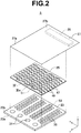
- FIG. 2 is a disassembled perspective view showing a portion of the head 5. Note that, the lower part on the drawing (negative side of the z-direction) in FIG. 2 is the media 101 side.
- the head 5 has a passage member 23 configuring passages of inks, a piezoelectric actuator substrate 25 which generates driving power for ejecting inks from the passage member 23, an FPC (flexible printed circuit) 27 which is electrically connected to the piezoelectric actuator substrate 25, and a driver IC 29 for performing driving and controlling the piezoelectric actuator substrate 25 through the FPC 27.
- a passage member 23 configuring passages of inks
- a piezoelectric actuator substrate 25 which generates driving power for ejecting inks from the passage member 23
- an FPC (flexible printed circuit) 27 which is electrically connected to the piezoelectric actuator substrate 25
- a driver IC 29 for performing driving and controlling the piezoelectric actuator substrate 25 through the FPC 27.
- the passage member 23 is for example substantially formed in a thin rectangular plate state and has a first major surface 23a facing the media 101 and a second major surface 23b of the back surface of the same. At the first major surface 23a, for ejecting ink drops, a plurality of nozzles which will be explained later are opened. Further, at the end part of the second major surface 23b, an ink supply port 31 to which the ink is supplied is formed for each color.
- the piezoelectric actuator substrate 25 is for example formed in a substantially thin rectangular plate state and is superimposed on the second major surface 23b of the passage member 23.
- the piezoelectric actuator substrate 25 is for example formed to a size large enough to cover the majority of the second major surface 23b (portion excluding region of arrangement for the plurality of ink supply ports 31).
- the FPC 27 for example has a facing portion 27a covering the piezoelectric actuator substrate 25 and an extension part 27b which extends outward from the facing portion 27a toward the outside of the piezoelectric actuator substrate 25.
- the extension part 27b may be provided in either of the main scanning direction or sub-scanning direction as well.
- the driver IC 29 is for example mounted on the extension part 27b. Note that, the driver IC 29 may be arranged at a suitable position by bending the FPC 27. Further, two extension parts may be provided on the FPC 27, and a driver IC 29 may be provided on each of these two extension parts (two driver ICs 29 may be provided in total).
- FIG. 3A is an enlarged plan view showing the passage member 23 and piezoelectric actuator substrate 25 in a region corresponding to the region IIIa in FIG. 2
- FIG. 3B is a cross-sectional view taken along the IIIb-IIIb line in FIG. 3A .
- the passage member 23 has a plurality of nozzles 33 opened in the first major surface 23a. Further, the passage member 23 has a plurality of pressurizing chambers 35 (see FIG. 2 as well) which are communicated with the plurality of nozzles 33 and are opened at the second major surface 23b side and has a common passage 37 ( FIG. 3B ) for supplying inks from the ink supply ports 31 to the plurality of pressurizing chambers 35.
- the concrete shapes may be suitably set.
- the planar shape of a pressurizing chamber 35 may also be roughly rectangular with a nozzle 33 connected to the center of a short side.
- the planar shape of a pressurizing chamber 35 may also be diamond shape with a nozzle 33 connected to a corner portion or may be an oval or elliptical shape with a nozzle 33 connected to a semicircular shape end part.
- the passage member 23 is for example configured by stacking a plurality of plate-shaped members 39 in the z-direction.
- the plurality of plate-shaped members 39 is formed with via holes or grooves which become the passages.
- the plurality of plate-shaped members 39 are for example made of a metal. Note that, the plate-shaped member 39 configuring the first major surface 23a may be configured by a resin, while the other plate-shaped members 39 may be configured by a metal and so on.
- the piezoelectric actuator substrate 25 is for example configured by a unimorph type piezoelectric actuator substrate and is configured by, from the passage member 23 side, an elastic body 41, a common electrode 43, a piezoelectric body 45, and a plurality of individual electrodes 47 (see FIG. 2 as well) stacked in that order. Note that, all of them are formed in layer shapes (plate shapes).
- the elastic body 41 configures the upper surfaces of the plurality of pressurizing chambers 35.
- the piezoelectric body 45 contracts in the surface direction according to the inverse piezoelectric effect. Due to this, the elastic body 41 warps to the pressurizing chamber 35 side. By utilization of this action, pressure is given to the inks in the pressurizing chambers 35, and ink drops are ejected from the nozzles 33.
- the elastic body 41, common electrode 43, and piezoelectric body 45 are provided over the plurality of pressurizing chambers 35 as a whole.
- an individual electrode 47 is provided for each pressurizing chamber 35.
- a reference potential is given to the common electrode 43.
- a potential (driving signal) which is different from that for the common electrode 43 is selectively given. Due to this, the ink drops are selectively ejected from the plurality of nozzles 33.
- Each of the plurality of individual electrodes 47 has an electrode body 47a which is superimposed over substantially the entirety of the pressurizing chamber 35 and is for applying voltage to the piezoelectric body 45 and has a leadout electrode 47b for connection with the FPC 27.
- the electrode body 47a is for example given a shape roughly the same as (resembling) the planar shape of the pressurizing chamber 35. In the present embodiment, the electrode body 47a is rectangular and is smaller than the pressurizing chamber 35.
- the leadout electrode 47b extends outward from the electrode body 47a to a suitable direction. For example, the leadout electrode 47b extends outward to the side opposite to the nozzle 33 with respect to the electrode body 47a and up to the position where it is not superimposed on the pressurizing chamber 35.
- the portion corresponding to one nozzle 33 (substantially a region of arrangement of a pressurizing chamber 35 and an individual electrode 47 when viewed by a plan view) will be sometimes referred to as an "ejection element 49".
- the plurality of ejection elements 49 are arranged in the main scanning direction and sub-scanning direction. Specifically, for example, this is as follows.
- Each of the plurality of ejection elements 49 is arranged so that the direction in which the nozzle 33 is arranged with respect to the pressurizing chamber 35 and in which the leadout electrode 47b extends with respect to the electrode body 47a is matched with the sub-scanning direction (x-direction).
- the plurality of ejection elements 49 are given the same orientations as each other. Between the ejection element rows 51 which are adjacent to each other, orientations of the nozzles 33 (leadout electrodes 47b) are made inverse to each other. Further, they are arranged offset from each other in the scanning direction by a size half of the ejection element 49 in the main scanning direction.
- Two ejection element rows 51 with the nozzle 33 sides facing each other correspond to one ink.
- eight ejection element rows 51 in total are provided corresponding to four colors. Note that, the number of the ejection element rows 51 may be different for each color. For example, the number of ejection element rows 51 may be made larger for black ink.
- a plurality of pressurizing chambers 35 are arranged in the main scanning direction (y-direction) to configure a pressurizing chamber row 53 ( FIG. 2 ) and the plurality of pressurizing chamber rows 53 are aligned in the sub scanning direction (x-direction).
- the common passage 37 is connected to the ink supply ports 31 and extends along the ejection element rows 51 (see FIG. 9 though it is a view of a modification).
- the driver IC 29 shown in FIG. 2 is electrically connected through the FPC 27 to the plurality of individual electrodes 47 and common electrode 43.
- data of the amount of ink to be ejected is input from the control part 11 for all nozzles 33 at each predetermined driving period.
- the driver IC 29 for example gives a reference potential to the common electrode 43 and selectively outputs driving signals having a predetermined waveform to the plurality of individual electrodes 47 based on the input data.
- FIG. 4 is a cross-sectional view taken along the IV-IV line in FIG. 2 for the plate-shaped member 39 in the uppermost layer of the passage member 23, piezoelectric actuator substrate 25, and FPC 27.
- the FPC 27 has an insulating base film 55, conductor pattern 57 formed on the base film 55, and an insulation film 59 covering the conductor pattern 57. Further, the facing portion 27a of the FPC 27 is arranged so as to make the insulation film 59 side face the piezoelectric actuator substrate 25 side.
- the base film 55 is for example made of a flexible resin film.
- the thickness of the base film 55 is for example about 20 ⁇ m to 200 ⁇ m.
- the conductor pattern 57 is for example made of metal such as copper.
- the thickness of the conductor pattern 57 is for example about 5 ⁇ m to 20 ⁇ m.
- the insulation film 59 is for example made of a solder resist.
- the solder resist is for example made of a thermosetting epoxy resin containing a pigment or the like.
- the thickness of the insulation film 59 is for example made thicker than the thickness of the conductor pattern 57 by about 5 ⁇ m to 20 ⁇ m.
- the conductor pattern 57 for example includes a plurality of interconnects 61 and not shown plurality of pads for connecting the driver IC 29 and the individual electrodes 47 and includes a not shown one or plurality of interconnects and a plurality of pads 63 for connecting the driver IC 29 and the common electrode 43.
- the plurality of interconnects 61 extend concurrently (for example in parallel) to each other along the ejection element rows 51 so that they are superimposed on the ejection element rows 51 (pressurizing chamber rows 53) and are bent outward and head toward the leadout electrodes 47b in order from the interconnect 61 which is positioned on the outside (lateral side) .
- pads are connected to the front ends thereof.
- the pads and the leadout electrodes 47b are joined by not shown bumps (however, similar to the bumps 65 explained later).
- the plurality of pads 63 are provided on the tips or middles of a not shown plurality of interconnects extending from the driver IC 29 and are joined to the connection patterns 67 of the piezoelectric actuator substrate 25 by the plurality of bumps 65.
- the thicknesses of the bumps 65 are for example about 5 ⁇ m to 20 ⁇ m.
- the plurality of pads 63 are for example positioned on the periphery of the facing portion 27a of the FPC 27 (the periphery of piezoelectric actuator substrate 25) . More specifically, the plurality of pads 63 are arranged along the edge parts in the edge parts on the two sides of the sub-scanning direction (x-direction) of the piezoelectric actuator substrate 25 as understood from the positions of the plurality of connection patterns 67 in FIG. 2 . Note, the plurality of pads 63 may be arranged along the edge parts in one, three, or four edge parts of the piezoelectric actuator substrate 25 as well.
- one interconnect may be connected to a suitable number of pads 63. Further, this one or a plurality of interconnects may be arranged at suitable positions in accordance with the positions of the plurality of pads 63. For example, in the present embodiment, the plurality of pads 63 are positioned at the edge parts of the facing portion 27a, therefore one or a plurality of interconnects may extend along the edge parts of the facing portion 27a.
- a bump 65 shown in FIG. 4 may be formed by a suitable material having conductivity.
- the bump 65 is comprised of a resin (for example thermosetting resin) containing particles made of metal (for example Ag).
- the insulation film 59 covers the plurality of interconnects 61 and not shown one or plurality of interconnects which are connected to the plurality of pads 63. Due to this, short-circuiting of the plurality of interconnects 61 etc. due to adhesion of the conductive material are reduced. Note that, at the insulation film 59, a not shown plurality of pads of the FPC 27, which are joined to the plurality of individual electrodes 47, and the plurality of pads 63 are exposed. Further, the insulation film 59 has a broadness large enough to be superimposed over at least a portion of the pressurizing chambers 35.
- the piezoelectric actuator substrate 25 in addition to the configuration explained with reference to FIGS. 3A and 3B , has a plurality of via conductors 69 which are arranged in the plurality of via holes 45h formed in the piezoelectric body 45 and are connected to the common electrode 45 and has the plurality of connection patterns 67 explained above which are connected to the plurality of via conductors 69. Accordingly, by connection of the connection patterns 67 to the FPC 27 by the bumps 65, the common electrode 43 is electrically connected to the driver IC 29.
- the plurality of via conductors 69 (plurality of via holes 45h) and plurality of connection patterns 67 are for example positioned at the two edge parts of the piezoelectric actuator substrate 25.
- the plurality of connection patterns 67 may be positioned at one, three, or four edge parts of the region for arrangement of the plurality of individual electrodes 47 as well.
- the connection patterns 67 are for example formed so as to extend from the positions on the via conductors 69 to directions along the edge parts of the piezoelectric actuator substrate 25 (y-direction) and are joined to the pads 63 by the bumps 65 at positions which are different from the positions on the via conductors 69.
- connection patterns 67 are for example comprised of the same conductive material as that for the individual electrodes 47 and have the same thickness as the individual electrodes 47. Note that, they may be configured by stacking a plurality of conductive layers as well. Further, the connection patterns 67 and the individual electrodes 47 may be comprised of materials which are different from each other and may be given thicknesses which are different from each other.
- the planar shapes of the connection patterns 67 may be made suitable ones. For example, the areas may be made broader in a pad state at the portions connected to the via conductors 69 and/or the portions connected to the bumps 65.
- the via conductors 69 may be formed by the same conductive material as that for the connection patterns 67 and/or common electrode 43 etc. or may be comprised of a different material.
- the planar shapes of the via conductors 69 (via holes 45h) may be made suitable shapes, for example, circles.
- the leadout electrodes 47b of the individual electrodes 47 and not shown pads of the FPC 27 are joined by not shown bumps. Further, the connection patterns 67 and the pads 63 of the FPC 27 are joined by the bumps 65. Due to this, the piezoelectric actuator substrate 25 and the facing portion 27a of the FPC 27 are fastened. Accordingly, the piezoelectric actuator substrate 25 and the facing portion 27a face each other in for example a state where the bumps 65 function as spacers.
- the insulation film 59 of the FPC 27 faces the electrode bodies 47a of the individual electrodes 47 and portions of the connection patterns 67 (tops of the via conductors 69 and peripheral portions thereof) at a very small interval or contacts the latter with a relatively low pressure.
- the size of the very small interval is for example 20 ⁇ m or less, or 10 ⁇ m or less.
- such a state is for example realized by joining the FPC 27 to the piezoelectric actuator substrate 25 like in the following way.
- an uncured material which will form the bumps for example, a thermosetting resin containing metal particles
- the FPC 27 is coated on the piezoelectric actuator substrate 25, and the FPC 27 is pressed against the piezoelectric actuator substrate 25.
- the material which will form the bumps is crushed (deforms) and thus the insulation film 59 contacts or approaches the piezoelectric actuator substrate 25.
- the material which will form the bumps is thermally cured.
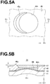
- FIG. 5A is a plan view near a via hole 45h of the piezoelectric body 45.
- FIG. 5B is a cross-sectional view of the piezoelectric actuator substrate 25 taken along the Vb-Vb line in FIG. 5A .
- connection pattern 67 enters into the upper part of the via hole 45h.
- the connection pattern 67 may be defined including this portion entered into the upper part of the via hole 45h or may be defined using the surface of the piezoelectric body 45 on the FPC 27 side as the standard (the portion entered into the upper part of the via hole 45h may be grasped as a portion of the via conductor 69 as well). Below, for convenience of the explanation, this will be explained according to the former definition.
- the piezoelectric body 45 has a projection portion 45p which projects to the FPC 27 side at the edge part of each via hole 45h.
- the height H1 ( FIG. 5B ) of the projection portion 45p from the flat surface of the piezoelectric body 45 is for example larger than the thickness of the individual electrode 47 and the thickness of a portion of the connection pattern 67 on the piezoelectric body 45 (the portion other than a portion on the via conductor 69).
- the top face of the projection portion 45p (the vertex or ridgeline having an extremely small area is also regarded as one type of top face) is positioned nearer to the FPC 27 side than the surface of the individual electrode 47 on the FPC 27 side. Further, the projection portion 45p penetrates through the connection pattern 67 and its top face is exposed to the FPC 27 side. Then, the top face of the projection portion 45p contacts the FPC 27 (insulation film 59) or faces the latter at a very small interval.
- the height of the projection portion 45p may be suitably set. As one example, this is 5 ⁇ m to 10 ⁇ m.
- the projection portion 45p is formed so as to extend along the edge part of the via hole 45h. Its length is for example 1/3 the circumference to 2/3 the circumference of the edge part of the via hole 45h.
- FIG. 5A exemplifies a case where the length of the projection portion 45p is about a half circumference of the edge part of the via hole 45h.
- the connection pattern 67 when viewed by a plan view, extends from the position superimposed on the via conductor 69 to the outside of the via conductor 69 through a portion in the edge part of the via hole 45h where the projection portion 45p is not formed.
- the cross-sectional shape and width etc. of the projection portion 45p may be suitably set.
- the cross-sectional shape is triangular, but may be a dome shape as well.
- the common electrode 43 and elastic body 41 are recessed to the via hole 45h side at the region at which they are superimposed over a via hole 45h. Accordingly, at the surface of the piezoelectric actuator substrate 25 (elastic body 41) on the passage member 23 side (negative side of z-direction), in the region superimposed over the via hole 45h, a recessed portion 41r is formed. The depth etc. of the recessed portion 41r may be suitably set.
- FIG. 6 is a flow chart showing an example of the procedure of the method of production of the piezoelectric actuator substrate 25.
- FIG. 7A to FIG. 7C are cross-sectional views corresponding to FIG. 5B for explaining the method of production of the piezoelectric actuator substrate. Note that, the states of the materials configuring the parts and shapes of the parts change along with the advance of the manufacturing process. However, for convenience of explanation, the same notations will be sometimes attached before and after the change.
- Steps ST1 to ST3 show the manufacturing procedure of the piezoelectric body 45.
- a ceramic green sheet which will form the piezoelectric body 45 is formed on a tape 71 ( FIG. 7A ) by tape casting.
- the tape 71, and green sheet which will form the piezoelectric body 45 are pressed in the lamination direction to adjust the shape of the green sheet.
- step ST3 as shown in FIG. 7A , by punching process (punching), the holes which will form the via holes 45h are formed in the green sheet which will form the piezoelectric body 45a.
- edge parts of holes which will form the via holes 45h are turned up (burrs and rollovers occur) in the punching direction.
- the punching is for example carried out in the direction from the green sheet side which will form the piezoelectric body 45 to the tape 71 side. Note, the inverse direction to that is also possible.
- Steps ST4 to ST6 which are carried out separately from steps ST1 to ST3 show the manufacturing procedure of the elastic body 41 and common electrode 43.
- a ceramic green sheet which will form the elastic body 41 is formed on a not shown tape by tape casting.
- the tape and the green sheet which will form the elastic body 41 are pressed in the lamination direction to adjust the shape of the green sheet.
- a conductive paste which will form the common electrode 43 is coated on the green sheet which will form the elastic body 41 by screen printing or the like.
- the green sheet which will form the piezoelectric body 45 and a laminate configured by the green sheet which will form the elastic body 41 and by the conductive paste which will form the common electrode 43 are adhered to each other.
- the side opposite to the direction where the edge part of the hole which will form the via hole 45h is turned up is made the common electrode 43 side (see FIG. 7B ).
- a conductive paste 79 which will form the via conductors 69 is filled by screen printing in the holes which will become the via holes 45h. That is, a printing plate 75 is placed over the piezoelectric body 45, a squeegee 77 is moved to the direction indicated by the arrow y11 while pressing the squeegee 77 against the printing plate 75, and the conductive paste 79 on the printing plate 75 is pushed to the piezoelectric body 45 side above the holes which will become the via holes 45h. At this time, the portions of the green sheet 45 other than the via holes 45h are covered by the tape 71. Therefore, in order to selectively print the conductive paste 79 at the via hole 45h portions, it is also possible to perform printing without using screen printing plate, metal mask, and so on.
- the turned up states of the portions (right side on the drawing sheet) which are turned up to the opposite side to the movement direction of the squeegee 77 are corrected.
- the turned up states are not corrected by the squeegee 77 or even if partially corrected the turned up states are remain.
- the portions (burrs) in which the turned up states are not corrected and remain configure the projection portions 45p.
- the holes which form the via holes 45h are circular, the turned up portions covering about half the circumference of the edge parts of the holes are not corrected and become the projection portions 45p.
- the green sheet which will form the elastic body 41, the conductive paste which will form the common electrode 43, and the green sheet which will form the piezoelectric body 45 are pressed in the lamination direction to adjust the shapes. Beneath the portions which will form the projection portions 45p (beneath the rollovers) at the green sheet which will form the piezoelectric body 45, conductive paste which will form the via conductors 69 is arranged. Therefore, in the portions which will form the projection portions 45p, the turned up states are not corrected or even if partially corrected the turned up states remain.
- the thickness of the conductive paste which will form the via conductors 69 is thinner than the thickness of the green sheet which will form the piezoelectric body 45 or the total thickness of the green sheet which will form the piezoelectric body 45 and the tape 71, therefore the conductive paste which will form the common electrode 43 and the green sheet which will form the elastic body 41 warp to the hole side which will form the via holes 45h and thus the recessed portions 41r are formed.
- step ST10 degreasing and firing are carried out. Note that, it is also possible to omit the degreasing. Note that, the tape 71 is peeled off before the degreasing.
- connection patterns 67 are for example formed by printing the conductive paste and firing it.
- the formation of the conductor patterns may be carried out by forming a metal film in predetermined patterns by a vapor deposition process through a mask or by etching after forming a metal film on the entire surface by a vapor deposition process. Note that, at the time of formation of the conductor patterns, patterning is carried out so that conductor patterns (connection patterns 67) are not formed on the projection portions 45p.
- the conductor patterns are formed by printing, it is also possible to keep the upper parts of the projection portions 45p from being printed by making the printing thickness thinner than the heights of the projection portions 45p. Further, it is also possible to utilize the fact that the general shapes of the projection portions 45p are tapered shapes and therefore it is hard for the metal film to adhere onto the projection portions 45p.
- the head 5 has the passage member 23 having the nozzles 33 and the pressurizing chambers 35 which are communicated with the nozzles 33 and are opened on the side opposite to the side where the nozzles 33 are opened, the piezoelectric actuator substrate 25 which is superimposed on the passage member 23 so as to close the pressurizing chambers 35, and the FPC 27 which faces the piezoelectric actuator substrate 25 from the side opposite to the passage member 23.
- the passage member 23 use may be made of one further having a plate-shaped member 39 so as to close the pressurizing chambers 35 on the side where the pressurizing chambers 35 are opened.
- the piezoelectric actuator substrate 25 has the piezoelectric body 45 which is exposed to the FPC 27 side.
- the piezoelectric body 45 has the via holes 45h which are opened toward the FPC 27 and has the projection portions 45p at the edge parts of the via holes 45h which project to the FPC 27 side.
- the projection portions 45p become spacers, so contact of the FPC 27 to the piezoelectric actuator substrate 25 is suppressed.
- the influence of the load of the FPC 27 exerted upon the operation of the piezoelectric actuator substrate 25 is reduced.
- abnormal noise in the head 5 due to the vibration of the FPC 27 due to the operation of the piezoelectric actuator substrate 25 is suppressed.
- dynamic interference between the FPC 27 and the piezoelectric actuator substrate 25 is reduced by the projection portions 45p.
- the projection portions 45p contribute also to suppression of too much crushing of the bumps 65 when joining the FPC 27 and the piezoelectric actuator substrate 25.
- the vibration on the pressurizing chambers 35 in the operation of the piezoelectric actuator substrate 25 is easily transmitted to the FPC 27 in a case where the interval between the individual electrodes 47 and the FPC 27 is the very small interval of 20 ⁇ m or less.
- the projection portions 45p it can be made harder for vibration of the FPC 27 to occur. That is, the projection portions 45p more effectively act in a case where the interval between the surfaces of the individual electrodes 47 which face the FPC 27 and the FPC 27 is 20 ⁇ m or less, further preferably 10 ⁇ m.
- the piezoelectric actuator substrate 25 further has the piezoelectric body 45 and the individual electrodes 47 which are superimposed on the FPC 27 side of the piezoelectric body 45 while avoiding the projection portions 45p.
- the top faces of the projection portions 45p are positioned nearer to the FPC 27 side than the surfaces of the individual electrodes 47 which face the FPC 27.
- the projection portions 45p have sufficient height. Therefore, the interference between the FPC 27 and the piezoelectric actuator substrate 25 which was explained above can be more reliably reduced. Further, the individual electrodes 47 are portions which are positioned on the pressurizing chambers 35 and vibrate, therefore the interference between the FPC 27 and the piezoelectric actuator substrate 25 can be more effectively reduced.
- the piezoelectric actuator substrate 25 further has the via conductors 69 which are arranged in the via holes 45h and connect the conductor layers (common electrode 43 and connection patterns 67) which are arranged at front and back sides of the piezoelectric body 45 to each other.
- the via holes 45h are formed so as to electrically connect the front and the back sides of the piezoelectric body 45 and are not ones (the ones are included in the invention of the present application as well) provided only for forming the projection portions 45p for reducing the interference between the FPC 27 and the piezoelectric actuator substrate 25. Accordingly, the configuration of the piezoelectric actuator substrate 25 is simple, and the method of production is simplified.
- the projection portions 45p are formed over 1/3 the circumference to 2/3 the circumference of the edge parts of the via holes 45h.
- connection patterns 67 can extend from the positions on the via holes 45h to the outside of the via holes 45h through the positions at which the projection portions 45p are not arranged. Therefore, compared with a case where the projection portions are formed over the entire circumferences of the via holes 45h (this case is included in the invention of the present application as well), electrical connection can be reliably established.
- the surface of the piezoelectric actuator substrate 25 which is joined to the passage member 23 is recessed at the regions superimposed over the via holes 45h (the recessed portions 41r are formed).
- FIG. 8 is a cross-sectional view corresponding to FIG. 5B and shows a modification of the cross-sectional structure around a projection portion 45p.
- a connection pattern 67 covers the projection portion 45p.
- the thickness of the portion on the projection portion 45p is for example substantially equal to the thickness of the portion in the connection pattern 67 which is located on the flat surface of the piezoelectric body 45 and to the thickness of the individual electrode 47.
- the top face of the portion on the projection portion 45p is positioned nearer to the FPC 27 side than the surface of the individual electrode 47 which faces the FPC 27.
- the projection portions 45p and the portions in the connection patterns 67 which are located on the projection portions 45p are made to function as spacers, therefore the dynamic interference between the FPC 27 and the piezoelectric actuator substrate 25 can be reduced.
- the portions of the connection patterns 67 which are located on the projection portions 45p also function as spacers, therefore the spacers can be easily made thicker.
- the heights of the projection portions 45p can be made lower. For example, even when the heights of the projection portions 45p are smaller than the thicknesses of the individual electrodes 47, the top faces of the connection patterns 67 which are located on the projection portions 45p are positioned nearer to the FPC 27 side than the surfaces of the individual electrodes 47, so contact between the FPC 27 and the individual electrodes 47 can be suppressed.
- connection patterns 67 in a configuration like in the embodiments where the projection portions 45p are not covered by the connection patterns 67, compared with the modification, for example, the possibility of unintended electrical connection between the piezoelectric actuator substrate 25 and the FPC 27 can be reduced.
- FIG. 9 is a plan view showing a modification of the positions of arrangement of the connection patterns 67 (via holes 45h, projection portions 45p, via conductors 69, pads 63, and bumps 65).
- connection patterns 67 are provided between the ejection element rows 51 (for example on the leadout electrode 47b side) in addition to or in place of the edge parts of the piezoelectric actuator substrate 25. More specifically, for example, the connection patterns 67 extend along the ejection element rows 51. Further, a plurality of connection patterns 67 are arranged along the ejection element rows 51. Further, although not particularly shown, the plurality of connection patterns 67 are provided in two or more rows corresponding to the provision of two or more sets (three sets in the example of FIG. 2 ) each consisting of two ejection element rows 51 in which the leadout electrodes 47b are made to face each other.
- the via holes 45h and via conductors 69 are positioned at the end parts on the positive side of the y-direction of the connection patterns 67
- the pads 63 and bumps 65 are positioned at the end parts on the negative side of the y-direction of the connection patterns 67
- the projection portions 45p are positioned at the edge parts on the positive side of the y-direction of the via holes 45h.
- the not shown interconnects of the FPC 27 which are connected to the pads 63 for example extend along the ejection element rows 51.
- the projection portions 45p which function as the spacers between the FPC 27 and the upper surface of the piezoelectric actuator substrate 25 are not only positioned on the periphery of the piezoelectric actuator substrate 25, but are also positioned between the ejection elements 49, therefore the interference between the FPC 27 and the piezoelectric actuator substrate 25 can be more reliably reduced.
- the aspect of providing the connection patterns 67 only on the periphery as in the embodiments is advantageous for reducing the size of the piezoelectric actuator substrate 25.
- the piezoelectric body 45 is one example of the insulation layer
- the individual electrodes 47 are examples of the external electrodes
- the common electrode 43 is one example of the internal electrode
- the common electrode 43 and connection patterns 67 are examples of the front and back conductive layers of the piezoelectric body.
- the number of layers of the piezoelectric body 45 may be set to two or more as well.
- the piezoelectric actuator substrate 25 is comprised of, for example, from the passage member 23 side, the elastic body 41, common electrode 43, piezoelectric body 45, plurality of individual electrodes 47, piezoelectric body 45, common electrode 43, piezoelectric body 45, and plurality of individual electrodes 47 laminated in that order. That is, in this configuration, between the common electrodes 43 and the plurality of individual electrodes 47 which are alternately arranged, three layers of the piezoelectric body 45 are arranged.
- the plurality of individual electrodes 47 and the plurality of individual electrodes 47 in another layer are individually electrically connected by the via conductors 69 which are arranged in the via holes 45h.
- the plurality of individual electrodes 47, in both layers, are arranged in the same way as shown in FIG. 2 .
- the via holes 45h and via conductors 69 are arranged in the leadout electrodes 47b at positions where they are not superimposed over the pressurizing chambers 35.
- the common electrode 43 which is arranged between the two layers each consisting of the plurality of individual electrodes 47 is arranged while avoiding the via conductors 69 which electrically connect the plurality of individual electrodes 47. Further, the two layers of common electrode 43 are electrically connected by the via conductors 69 arranged in the via holes 45h.
- the projection portion 45p projecting to the FPC 27 side is arranged in the edge part of the via hole 45h which is arranged at each leadout electrode 47b.
- the electrode body 47a which is arranged on the pressurizing chamber 35 is arranged so as to avoid the projection portion 45p. Therefore, it becomes harder to cause interference between the FPC 27 which is pushed upward by the projection portion 45p and the electrode body 47a.
- the electrode body 47a is one example of the external electrode.
- the printer is not limited to the serial head type and off-carriage type.
- the printer may be a line head type and/or on-carriage type as well.
- the piezoelectric actuator substrate is not limited to a unimorph type and for example may be a bimorph type as well.
- the configurations of the portions other than the inkjet head in the printer may be suitable configurations other than the exemplified configurations.
- the media are not limited to paper either and may be media made of metal or resin.
- the insulation layer exposed on the flexible board side and having via holes formed therein is not limited to the piezoelectric body and for example may be a reinforcing layer which covers the piezoelectric body and reinforces the piezoelectric actuator substrate.
- the via holes are not limited to ones for arranging via conductors and for example may be dedicated holes which are formed for forming the projection portions or may be openings in the above-explained reinforcing layer which are formed on the pressurizing chambers so that the bending of the piezoelectric body to the pressurizing chambers are not obstructed.
- connection patterns shown in the embodiments may be connected to each other to form a single connection pattern as well.
Landscapes
- Engineering & Computer Science (AREA)
- Manufacturing & Machinery (AREA)
- Particle Formation And Scattering Control In Inkjet Printers (AREA)
Description
- The present invention relates to an inkjet head and a printer.
- Known in the art is a piezo-type inkjet head (for example, Patent Literature 1) . This type of inkjet head has a passage member in which a passage for ink is formed, a piezoelectric actuator substrate superimposed on the passage member, and a flexible printed circuit covering the surface of the piezoelectric actuator substrate on the side opposite to the passage member. The passage member has a nozzle for ejecting ink and a pressurizing chamber which is communicated with the nozzle and is opened on the opposite side to the opening direction of the nozzle. The piezoelectric actuator substrate closes the pressurizing chamber, bends into the pressurizing chamber due to an inverse piezoelectric effect when voltage is applied, and gives a pressure to the ink in the pressurizing chamber. Due to this, the ink is ejected from the nozzle. The flexible printed circuit electrically mediates between the piezoelectric actuator substrate and a driver driving and controlling the piezoelectric actuator substrate.
-
Patent Literature 1. Japanese Patent Publication No.2010-105317A - In the configuration as described above, the piezoelectric actuator substrate and the flexible printed circuit covering this are liable to dynamically interfere. For example, the load of the flexible printed circuit is liable to be added to the piezoelectric actuator substrate, and this load is liable to exert an effect upon deflection by the inverse piezoelectric effect in the piezoelectric actuator substrate. Further, for example, the flexible printed circuit is liable to vibrate due to the operation of the piezoelectric actuator substrate and strange noise unpleasant to the user is liable to be generated.
- Accordingly, desirably there is provided an inkjet head capable of reducing interference between a piezoelectric actuator substrate and a flexible printed circuit.
- An inkjet head according to one aspect of the present invention has a passage member having a nozzle and a pressurizing chamber which is communicated with the nozzle and is positioned on the opposite side to the side at which the nozzle is opened, a piezoelectric actuator substrate which is superimposed on the passage member so as to cover the pressurizing chamber, and a flexible printed circuit which faces the piezoelectric actuator substrate from the side opposite to the passage member. The piezoelectric actuator substrate has an insulation layer which is exposed on the flexible printed circuit side. The insulation layer has a via hole opened toward the flexible printed circuit and has a projection portion which projects to the flexible printed circuit side at the edge part of the via hole.
- A printer according to an aspect of the present invention is provided with the above inkjet head, a scanning portion which makes media and the inkjet head move relative to each other and a control part which controls the inkjet head.
- According to the above configuration, interference between the piezoelectric actuator substrate and the flexible printed circuit can be reduced.
-
- [
FIG. 1 ] A perspective view substantially showing principal parts of a printer according to an embodiment of the present invention. - [
FIG. 2 ] A disassembled perspective view substantially showing a portion of an inkjet head of the printer inFIG. 1 . - [
FIGS. 3A and 3B] FIG. 3A is a plan view in a region IIIa inFIG. 2 , andFIG. 3B is a cross-sectional view taken along the IIIb-IIIb line inFIG. 3A . - [
FIG. 4 ] A cross-sectional view taken along the IV-IV line inFIG. 2 . - [
FIGS. 5A and 5B] FIG. 5A is a plan view near a via hole of a piezoelectric body, andFIG. 5B is a cross-sectional view of a piezoelectric actuator substrate taken along the Vb-Vb line inFIG. 5A . - [
FIG. 6 ] A flow chart showing a procedure of a method of production of the piezoelectric actuator substrate. - [
FIGS. 7A to 7C] FIG. 7A to FIG. 7C are cross-sectional views for explaining the method of production of the piezoelectric actuator substrate. - [
FIG. 8 ] A cross-sectional view showing a modification of the piezoelectric actuator substrate. - [
FIG. 9 ] A plan view showing another modification of the piezoelectric actuator substrate. -
FIG. 1 is a perspective view substantially showing principal parts of aprinter 1 according to an embodiment of the present invention. - The
printer 1 is an inkjet printer. More specifically, for example, theprinter 1 is a piezo-head type, serial head type, and off-carriage type color printer. Note that, theprinter 1 may realize a colored image by inks of a suitable number of colors. In the present embodiment, however, the color image is realized by inks of four colors (black, yellow, magenta, and cyan). - The
printer 1 for example has conveyingportions 3 which convey media (for example paper) 101 to a conveyance direction indicated by an arrow y1, ahead 5 which ejects ink drops toward themedia 101 which are being conveyed, ascanning portion 7 which makes thehead 5 reciprocally move in a sub-scanning direction (arrow y2) which is perpendicular to the conveyance direction of themedia 101, ink cartridges 9 for supplying inks to thehead 5, and acontrol part 11 which controls the operation of theprinter 1 including an ejection operation of inks from thehead 5. - Ink drops are ejected from the
head 5 to amedium 101 repeatedly within a range broadened to main scanning direction perpendicular to the sub-scanning direction while thescanning portion 7 is making thehead 5 reciprocally move. By doing this, a belt-like two-dimensional image is formed on themedium 101. Further, by intermittent conveyance of themedium 101 by the conveyingportions 3, the belt-like two-dimensional images are connected and a continuous two-dimensional image is formed on themedium 101. - The conveying
portions 3 for example convey a plurality ofmedia 101 from a not shown supply stack one by one to a not shown delivery stack. The conveyingportions 3 may be given a known suitable configuration.FIG. 1 exemplifies conveyingportions 3 wherein the conveyance path is made to straight path and havingrollers 13 abutting against themedia 101,motors 15 rotating therollers 13, anddrivers 17 giving driving electrical power to themotors 15. - The
scanning portion 7 may be given a known suitable configuration. For example, thescanning portion 7 has a not shown guide rail which supports a not shown carriage on which thehead 5 is mounted so that the carriage can be guided in the sub-scanning direction, a not shown belt fixed to the carriage, a not shown pulley over which the belt is bridged, amotor 19 rotating the pulley, and adriver 21 giving driving electrical power to themotor 19. - The ink cartridges 9 are provided in a place different from that for the head 5 (so that the ink cartridges 9 will not move together with the head 5) . The ink cartridges 9 are connected through flexible tubes to the
head 5. A plurality of (four in the present embodiment) ink cartridges 9 are provided corresponding to the number of colors of ink ejected by thehead 5. - The
control part 11 includes for example a CPU, ROM, RAM, and external memory device. Thecontrol part 11 outputs control signals to thedrivers 17 of the conveyingportions 3, thedriver 21 of thescanning portion 7, and a driver (which will be explained later) of thehead 5 and controls operations of the conveyingportions 3,scanning portion 7, andhead 5. -
FIG. 2 is a disassembled perspective view showing a portion of thehead 5. Note that, the lower part on the drawing (negative side of the z-direction) inFIG. 2 is themedia 101 side. - The
head 5 has apassage member 23 configuring passages of inks, apiezoelectric actuator substrate 25 which generates driving power for ejecting inks from thepassage member 23, an FPC (flexible printed circuit) 27 which is electrically connected to thepiezoelectric actuator substrate 25, and adriver IC 29 for performing driving and controlling thepiezoelectric actuator substrate 25 through theFPC 27. - The
passage member 23 is for example substantially formed in a thin rectangular plate state and has a firstmajor surface 23a facing themedia 101 and a secondmajor surface 23b of the back surface of the same. At the firstmajor surface 23a, for ejecting ink drops, a plurality of nozzles which will be explained later are opened. Further, at the end part of the secondmajor surface 23b, anink supply port 31 to which the ink is supplied is formed for each color. - The
piezoelectric actuator substrate 25 is for example formed in a substantially thin rectangular plate state and is superimposed on the secondmajor surface 23b of thepassage member 23. Thepiezoelectric actuator substrate 25 is for example formed to a size large enough to cover the majority of the secondmajor surface 23b (portion excluding region of arrangement for the plurality of ink supply ports 31). - The
FPC 27 for example has a facingportion 27a covering thepiezoelectric actuator substrate 25 and anextension part 27b which extends outward from the facingportion 27a toward the outside of thepiezoelectric actuator substrate 25. Note that, theextension part 27b may be provided in either of the main scanning direction or sub-scanning direction as well. - The
driver IC 29 is for example mounted on theextension part 27b. Note that, thedriver IC 29 may be arranged at a suitable position by bending theFPC 27. Further, two extension parts may be provided on theFPC 27, and adriver IC 29 may be provided on each of these two extension parts (twodriver ICs 29 may be provided in total). -
FIG. 3A is an enlarged plan view showing thepassage member 23 andpiezoelectric actuator substrate 25 in a region corresponding to the region IIIa inFIG. 2 , andFIG. 3B is a cross-sectional view taken along the IIIb-IIIb line inFIG. 3A . - As already explained, the
passage member 23 has a plurality ofnozzles 33 opened in the firstmajor surface 23a. Further, thepassage member 23 has a plurality of pressurizing chambers 35 (seeFIG. 2 as well) which are communicated with the plurality ofnozzles 33 and are opened at the secondmajor surface 23b side and has a common passage 37 (FIG. 3B ) for supplying inks from theink supply ports 31 to the plurality of pressurizingchambers 35. - Note that, the concrete shapes may be suitably set. For example, as shown in the present embodiment, the planar shape of a pressurizing
chamber 35 may also be roughly rectangular with anozzle 33 connected to the center of a short side. Further, for example, the planar shape of a pressurizingchamber 35 may also be diamond shape with anozzle 33 connected to a corner portion or may be an oval or elliptical shape with anozzle 33 connected to a semicircular shape end part. - The
passage member 23 is for example configured by stacking a plurality of plate-shapedmembers 39 in the z-direction. The plurality of plate-shapedmembers 39 is formed with via holes or grooves which become the passages. The plurality of plate-shapedmembers 39 are for example made of a metal. Note that, the plate-shapedmember 39 configuring the firstmajor surface 23a may be configured by a resin, while the other plate-shapedmembers 39 may be configured by a metal and so on. - The
piezoelectric actuator substrate 25 is for example configured by a unimorph type piezoelectric actuator substrate and is configured by, from thepassage member 23 side, anelastic body 41, acommon electrode 43, apiezoelectric body 45, and a plurality of individual electrodes 47 (seeFIG. 2 as well) stacked in that order. Note that, all of them are formed in layer shapes (plate shapes). - The
elastic body 41 configures the upper surfaces of the plurality of pressurizingchambers 35. When voltage is applied between theindividual electrodes 47 and thecommon electrode 43, thepiezoelectric body 45 contracts in the surface direction according to the inverse piezoelectric effect. Due to this, theelastic body 41 warps to the pressurizingchamber 35 side. By utilization of this action, pressure is given to the inks in the pressurizingchambers 35, and ink drops are ejected from thenozzles 33. - The
elastic body 41,common electrode 43, andpiezoelectric body 45 are provided over the plurality of pressurizingchambers 35 as a whole. On the other hand, anindividual electrode 47 is provided for each pressurizingchamber 35. To thecommon electrode 43, for example, a reference potential is given. To the plurality ofindividual electrodes 47, a potential (driving signal) which is different from that for thecommon electrode 43 is selectively given. Due to this, the ink drops are selectively ejected from the plurality ofnozzles 33. - Each of the plurality of
individual electrodes 47 has anelectrode body 47a which is superimposed over substantially the entirety of the pressurizingchamber 35 and is for applying voltage to thepiezoelectric body 45 and has aleadout electrode 47b for connection with theFPC 27. Theelectrode body 47a is for example given a shape roughly the same as (resembling) the planar shape of the pressurizingchamber 35. In the present embodiment, theelectrode body 47a is rectangular and is smaller than the pressurizingchamber 35. Theleadout electrode 47b extends outward from theelectrode body 47a to a suitable direction. For example, theleadout electrode 47b extends outward to the side opposite to thenozzle 33 with respect to theelectrode body 47a and up to the position where it is not superimposed on the pressurizingchamber 35. - Note that, below, in the
passage member 23 andpiezoelectric actuator substrate 25 shown inFIGS. 3A and 3B , the portion corresponding to one nozzle 33 (substantially a region of arrangement of a pressurizingchamber 35 and anindividual electrode 47 when viewed by a plan view) will be sometimes referred to as an "ejection element 49". - As shown in
FIG. 2 , the plurality ofejection elements 49 are arranged in the main scanning direction and sub-scanning direction. Specifically, for example, this is as follows. - Each of the plurality of
ejection elements 49 is arranged so that the direction in which thenozzle 33 is arranged with respect to the pressurizingchamber 35 and in which theleadout electrode 47b extends with respect to theelectrode body 47a is matched with the sub-scanning direction (x-direction). - In the row of ejection elements 49 (ejection element row 51) configured by arrangement of a plurality of
ejection elements 49 in the main scanning direction (y-direction), the plurality ofejection elements 49 are given the same orientations as each other. Between theejection element rows 51 which are adjacent to each other, orientations of the nozzles 33 (leadout electrodes 47b) are made inverse to each other. Further, they are arranged offset from each other in the scanning direction by a size half of theejection element 49 in the main scanning direction. - Two
ejection element rows 51 with thenozzle 33 sides facing each other correspond to one ink. In the present embodiment, eightejection element rows 51 in total are provided corresponding to four colors. Note that, the number of theejection element rows 51 may be different for each color. For example, the number ofejection element rows 51 may be made larger for black ink. - Note that, as apparent from the fact that a plurality of
ejection elements 49 configure a plurality ofejection element rows 51, a plurality of pressurizingchambers 35 are arranged in the main scanning direction (y-direction) to configure a pressurizing chamber row 53 (FIG. 2 ) and the plurality of pressurizingchamber rows 53 are aligned in the sub scanning direction (x-direction). - The
common passage 37 is connected to theink supply ports 31 and extends along the ejection element rows 51 (seeFIG. 9 though it is a view of a modification). - The
driver IC 29 shown inFIG. 2 is electrically connected through theFPC 27 to the plurality ofindividual electrodes 47 andcommon electrode 43. To thedriver IC 29, for example, data of the amount of ink to be ejected is input from thecontrol part 11 for allnozzles 33 at each predetermined driving period. Thedriver IC 29 for example gives a reference potential to thecommon electrode 43 and selectively outputs driving signals having a predetermined waveform to the plurality ofindividual electrodes 47 based on the input data. Further, thedriver IC 29, for example, based on the input data, outputs one of a plurality of driving vibrations which are prepared in advance in the driving period or sets the number of times of outputting the driving signal. -
FIG. 4 is a cross-sectional view taken along the IV-IV line inFIG. 2 for the plate-shapedmember 39 in the uppermost layer of thepassage member 23,piezoelectric actuator substrate 25, andFPC 27. - The
FPC 27 has an insulatingbase film 55,conductor pattern 57 formed on thebase film 55, and aninsulation film 59 covering theconductor pattern 57. Further, the facingportion 27a of theFPC 27 is arranged so as to make theinsulation film 59 side face thepiezoelectric actuator substrate 25 side. - The
base film 55 is for example made of a flexible resin film. The thickness of thebase film 55 is for example about 20 µm to 200 µm. Theconductor pattern 57 is for example made of metal such as copper. The thickness of theconductor pattern 57 is for example about 5 µm to 20 µm. Theinsulation film 59 is for example made of a solder resist. The solder resist is for example made of a thermosetting epoxy resin containing a pigment or the like. The thickness of theinsulation film 59 is for example made thicker than the thickness of theconductor pattern 57 by about 5 µm to 20 µm. - The
conductor pattern 57 for example includes a plurality ofinterconnects 61 and not shown plurality of pads for connecting thedriver IC 29 and theindividual electrodes 47 and includes a not shown one or plurality of interconnects and a plurality ofpads 63 for connecting thedriver IC 29 and thecommon electrode 43. - The plurality of
interconnects 61, for example, although not particularly shown, extend concurrently (for example in parallel) to each other along theejection element rows 51 so that they are superimposed on the ejection element rows 51 (pressurizing chamber rows 53) and are bent outward and head toward theleadout electrodes 47b in order from theinterconnect 61 which is positioned on the outside (lateral side) . To the front ends thereof, not shown pads are connected. The pads and theleadout electrodes 47b are joined by not shown bumps (however, similar to thebumps 65 explained later). - The plurality of
pads 63 are provided on the tips or middles of a not shown plurality of interconnects extending from thedriver IC 29 and are joined to theconnection patterns 67 of thepiezoelectric actuator substrate 25 by the plurality ofbumps 65. The thicknesses of thebumps 65 are for example about 5 µm to 20 µm. - The plurality of pads 63 (and plurality of bumps 65) are for example positioned on the periphery of the facing
portion 27a of the FPC 27 (the periphery of piezoelectric actuator substrate 25) . More specifically, the plurality ofpads 63 are arranged along the edge parts in the edge parts on the two sides of the sub-scanning direction (x-direction) of thepiezoelectric actuator substrate 25 as understood from the positions of the plurality ofconnection patterns 67 inFIG. 2 . Note, the plurality ofpads 63 may be arranged along the edge parts in one, three, or four edge parts of thepiezoelectric actuator substrate 25 as well. - Among the not shown interconnects connecting the
driver IC 29 and the plurality ofpads 63, one interconnect may be connected to a suitable number ofpads 63. Further, this one or a plurality of interconnects may be arranged at suitable positions in accordance with the positions of the plurality ofpads 63. For example, in the present embodiment, the plurality ofpads 63 are positioned at the edge parts of the facingportion 27a, therefore one or a plurality of interconnects may extend along the edge parts of the facingportion 27a. - A
bump 65 shown inFIG. 4 may be formed by a suitable material having conductivity. For example, thebump 65 is comprised of a resin (for example thermosetting resin) containing particles made of metal (for example Ag). - The
insulation film 59 covers the plurality ofinterconnects 61 and not shown one or plurality of interconnects which are connected to the plurality ofpads 63. Due to this, short-circuiting of the plurality ofinterconnects 61 etc. due to adhesion of the conductive material are reduced. Note that, at theinsulation film 59, a not shown plurality of pads of theFPC 27, which are joined to the plurality ofindividual electrodes 47, and the plurality ofpads 63 are exposed. Further, theinsulation film 59 has a broadness large enough to be superimposed over at least a portion of the pressurizingchambers 35. - The
piezoelectric actuator substrate 25, in addition to the configuration explained with reference toFIGS. 3A and 3B , has a plurality of viaconductors 69 which are arranged in the plurality of viaholes 45h formed in thepiezoelectric body 45 and are connected to thecommon electrode 45 and has the plurality ofconnection patterns 67 explained above which are connected to the plurality of viaconductors 69. Accordingly, by connection of theconnection patterns 67 to theFPC 27 by thebumps 65, thecommon electrode 43 is electrically connected to thedriver IC 29. - As shown in
FIG. 2 andFIG. 4 , the plurality of via conductors 69 (plurality of viaholes 45h) and plurality ofconnection patterns 67 are for example positioned at the two edge parts of thepiezoelectric actuator substrate 25. Note that, as described in the explanation of the plurality ofpads 63, the plurality ofconnection patterns 67 may be positioned at one, three, or four edge parts of the region for arrangement of the plurality ofindividual electrodes 47 as well. Theconnection patterns 67 are for example formed so as to extend from the positions on the viaconductors 69 to directions along the edge parts of the piezoelectric actuator substrate 25 (y-direction) and are joined to thepads 63 by thebumps 65 at positions which are different from the positions on the viaconductors 69. - The
connection patterns 67 are for example comprised of the same conductive material as that for theindividual electrodes 47 and have the same thickness as theindividual electrodes 47. Note that, they may be configured by stacking a plurality of conductive layers as well. Further, theconnection patterns 67 and theindividual electrodes 47 may be comprised of materials which are different from each other and may be given thicknesses which are different from each other. The planar shapes of theconnection patterns 67 may be made suitable ones. For example, the areas may be made broader in a pad state at the portions connected to the viaconductors 69 and/or the portions connected to thebumps 65. - The via
conductors 69 may be formed by the same conductive material as that for theconnection patterns 67 and/orcommon electrode 43 etc. or may be comprised of a different material. The planar shapes of the via conductors 69 (viaholes 45h) may be made suitable shapes, for example, circles. - As explained above, the
leadout electrodes 47b of theindividual electrodes 47 and not shown pads of theFPC 27 are joined by not shown bumps. Further, theconnection patterns 67 and thepads 63 of theFPC 27 are joined by thebumps 65. Due to this, thepiezoelectric actuator substrate 25 and the facingportion 27a of theFPC 27 are fastened. Accordingly, thepiezoelectric actuator substrate 25 and the facingportion 27a face each other in for example a state where thebumps 65 function as spacers. - Specifically, for example, the
insulation film 59 of theFPC 27 faces theelectrode bodies 47a of theindividual electrodes 47 and portions of the connection patterns 67 (tops of the viaconductors 69 and peripheral portions thereof) at a very small interval or contacts the latter with a relatively low pressure. The size of the very small interval is for example 20 µm or less, or 10 µm or less. - Note that, such a state is for example realized by joining the
FPC 27 to thepiezoelectric actuator substrate 25 like in the following way. First, on theleadout electrodes 47b andconnection patterns 67, an uncured material which will form the bumps (for example, a thermosetting resin containing metal particles) is coated. Next, theFPC 27 is coated on thepiezoelectric actuator substrate 25, and theFPC 27 is pressed against thepiezoelectric actuator substrate 25. At this time, the material which will form the bumps is crushed (deforms) and thus theinsulation film 59 contacts or approaches thepiezoelectric actuator substrate 25. After that, the material which will form the bumps is thermally cured. -
FIG. 5A is a plan view near a viahole 45h of thepiezoelectric body 45.FIG. 5B is a cross-sectional view of thepiezoelectric actuator substrate 25 taken along the Vb-Vb line inFIG. 5A . - Note that, in
FIG. 5B , the material which configures theconnection pattern 67 enters into the upper part of the viahole 45h. Theconnection pattern 67 may be defined including this portion entered into the upper part of the viahole 45h or may be defined using the surface of thepiezoelectric body 45 on theFPC 27 side as the standard (the portion entered into the upper part of the viahole 45h may be grasped as a portion of the viaconductor 69 as well). Below, for convenience of the explanation, this will be explained according to the former definition. - As shown in
FIG. 4 ,FIG. 5A, and FIG. 5B , thepiezoelectric body 45 has aprojection portion 45p which projects to theFPC 27 side at the edge part of each viahole 45h. The height H1 (FIG. 5B ) of theprojection portion 45p from the flat surface of thepiezoelectric body 45 is for example larger than the thickness of theindividual electrode 47 and the thickness of a portion of theconnection pattern 67 on the piezoelectric body 45 (the portion other than a portion on the via conductor 69). Accordingly, the top face of theprojection portion 45p (the vertex or ridgeline having an extremely small area is also regarded as one type of top face) is positioned nearer to theFPC 27 side than the surface of theindividual electrode 47 on theFPC 27 side. Further, theprojection portion 45p penetrates through theconnection pattern 67 and its top face is exposed to theFPC 27 side. Then, the top face of theprojection portion 45p contacts the FPC 27 (insulation film 59) or faces the latter at a very small interval. The height of theprojection portion 45p may be suitably set. As one example, this is 5 µm to 10 µm. - As shown in
FIG. 5A , theprojection portion 45p is formed so as to extend along the edge part of the viahole 45h. Its length is for example 1/3 the circumference to 2/3 the circumference of the edge part of the viahole 45h.FIG. 5A exemplifies a case where the length of theprojection portion 45p is about a half circumference of the edge part of the viahole 45h. Theconnection pattern 67, when viewed by a plan view, extends from the position superimposed on the viaconductor 69 to the outside of the viaconductor 69 through a portion in the edge part of the viahole 45h where theprojection portion 45p is not formed. The cross-sectional shape and width etc. of theprojection portion 45p may be suitably set. InFIG. 5B , the cross-sectional shape is triangular, but may be a dome shape as well. - The
common electrode 43 andelastic body 41 are recessed to the viahole 45h side at the region at which they are superimposed over a viahole 45h. Accordingly, at the surface of the piezoelectric actuator substrate 25 (elastic body 41) on thepassage member 23 side (negative side of z-direction), in the region superimposed over the viahole 45h, a recessedportion 41r is formed. The depth etc. of the recessedportion 41r may be suitably set. -
FIG. 6 is a flow chart showing an example of the procedure of the method of production of thepiezoelectric actuator substrate 25.FIG. 7A to FIG. 7C are cross-sectional views corresponding toFIG. 5B for explaining the method of production of the piezoelectric actuator substrate. Note that, the states of the materials configuring the parts and shapes of the parts change along with the advance of the manufacturing process. However, for convenience of explanation, the same notations will be sometimes attached before and after the change. - Steps ST1 to ST3 show the manufacturing procedure of the
piezoelectric body 45. At step ST1, a ceramic green sheet which will form thepiezoelectric body 45 is formed on a tape 71 (FIG. 7A ) by tape casting. At step ST2, thetape 71, and green sheet which will form thepiezoelectric body 45 are pressed in the lamination direction to adjust the shape of the green sheet. - At step ST3, as shown in
FIG. 7A , by punching process (punching), the holes which will form the viaholes 45h are formed in the green sheet which will form the piezoelectric body 45a. At this time, in the green sheet which will form thepiezoelectric body 45 and thetape 71, edge parts of holes which will form the viaholes 45h are turned up (burrs and rollovers occur) in the punching direction. Note that, the punching is for example carried out in the direction from the green sheet side which will form thepiezoelectric body 45 to thetape 71 side. Note, the inverse direction to that is also possible. - Steps ST4 to ST6 which are carried out separately from steps ST1 to ST3 show the manufacturing procedure of the
elastic body 41 andcommon electrode 43. At step ST4, a ceramic green sheet which will form theelastic body 41 is formed on a not shown tape by tape casting. At step ST5, the tape and the green sheet which will form theelastic body 41 are pressed in the lamination direction to adjust the shape of the green sheet. At step ST6, a conductive paste which will form thecommon electrode 43 is coated on the green sheet which will form theelastic body 41 by screen printing or the like. - At step ST7, the green sheet which will form the
piezoelectric body 45 and a laminate configured by the green sheet which will form theelastic body 41 and by the conductive paste which will form thecommon electrode 43 are adhered to each other. At this time, in the green sheet which will form thepiezoelectric body 45, the side opposite to the direction where the edge part of the hole which will form the viahole 45h is turned up is made thecommon electrode 43 side (seeFIG. 7B ). - At step ST8, as shown in
FIG. 7B , aconductive paste 79 which will form the viaconductors 69 is filled by screen printing in the holes which will become the viaholes 45h. That is, aprinting plate 75 is placed over thepiezoelectric body 45, asqueegee 77 is moved to the direction indicated by the arrow y11 while pressing thesqueegee 77 against theprinting plate 75, and theconductive paste 79 on theprinting plate 75 is pushed to thepiezoelectric body 45 side above the holes which will become the viaholes 45h. At this time, the portions of thegreen sheet 45 other than the via holes 45h are covered by thetape 71. Therefore, in order to selectively print theconductive paste 79 at the viahole 45h portions, it is also possible to perform printing without using screen printing plate, metal mask, and so on. - At this time, as shown in
FIG. 7C , at the edge parts of the holes which will form the viaholes 45h, the turned up states of the portions (right side on the drawing sheet) which are turned up to the opposite side to the movement direction of thesqueegee 77 are corrected. On the other hand, at the portions which are turned up to the movement direction of thesqueegee 77 , the turned up states are not corrected by thesqueegee 77 or even if partially corrected the turned up states are remain. Further, the portions (burrs) in which the turned up states are not corrected and remain configure theprojection portions 45p. In the case where the holes which form the viaholes 45h are circular, the turned up portions covering about half the circumference of the edge parts of the holes are not corrected and become theprojection portions 45p. - At step ST9, the green sheet which will form the
elastic body 41, the conductive paste which will form thecommon electrode 43, and the green sheet which will form thepiezoelectric body 45 are pressed in the lamination direction to adjust the shapes. Beneath the portions which will form theprojection portions 45p (beneath the rollovers) at the green sheet which will form thepiezoelectric body 45, conductive paste which will form the viaconductors 69 is arranged. Therefore, in the portions which will form theprojection portions 45p, the turned up states are not corrected or even if partially corrected the turned up states remain. Further, the thickness of the conductive paste which will form the viaconductors 69 is thinner than the thickness of the green sheet which will form thepiezoelectric body 45 or the total thickness of the green sheet which will form thepiezoelectric body 45 and thetape 71, therefore the conductive paste which will form thecommon electrode 43 and the green sheet which will form theelastic body 41 warp to the hole side which will form the viaholes 45h and thus the recessedportions 41r are formed. - At step ST10, degreasing and firing are carried out. Note that, it is also possible to omit the degreasing. Note that, the
tape 71 is peeled off before the degreasing. - At step ST11, the
individual electrodes 47,connection patterns 67, and other conductor patterns of thepiezoelectric actuator substrate 25 on theFPC 27 side are formed. The conductor patterns are for example formed by printing the conductive paste and firing it. Other than the above description, the formation of the conductor patterns may be carried out by forming a metal film in predetermined patterns by a vapor deposition process through a mask or by etching after forming a metal film on the entire surface by a vapor deposition process. Note that, at the time of formation of the conductor patterns, patterning is carried out so that conductor patterns (connection patterns 67) are not formed on theprojection portions 45p. When the conductor patterns are formed by printing, it is also possible to keep the upper parts of theprojection portions 45p from being printed by making the printing thickness thinner than the heights of theprojection portions 45p. Further, it is also possible to utilize the fact that the general shapes of theprojection portions 45p are tapered shapes and therefore it is hard for the metal film to adhere onto theprojection portions 45p. - As described above, in the present embodiment, the
head 5 has thepassage member 23 having thenozzles 33 and the pressurizingchambers 35 which are communicated with thenozzles 33 and are opened on the side opposite to the side where thenozzles 33 are opened, thepiezoelectric actuator substrate 25 which is superimposed on thepassage member 23 so as to close the pressurizingchambers 35, and theFPC 27 which faces thepiezoelectric actuator substrate 25 from the side opposite to thepassage member 23. As thepassage member 23, use may be made of one further having a plate-shapedmember 39 so as to close the pressurizingchambers 35 on the side where the pressurizingchambers 35 are opened. By arranging the pressurizingchambers 35 on the secondmajor surface 23b side in thepassage member 23, the pressure generated at thepiezoelectric actuator substrate 25 which is arranged so as to cover the pressurizingchambers 35 is transmitted to the pressurizingchambers 35 through the plate-shapedmember 39 on the pressurizingchambers 35. Due to such a configuration, for example, the possibility of the solvent etc. of the ink exerting an influence upon the reliability of thepiezoelectric actuator substrate 25 can be reduced. Thepiezoelectric actuator substrate 25 has thepiezoelectric body 45 which is exposed to theFPC 27 side. Thepiezoelectric body 45 has the via holes 45h which are opened toward theFPC 27 and has theprojection portions 45p at the edge parts of the via holes 45h which project to theFPC 27 side. - Accordingly, the
projection portions 45p become spacers, so contact of theFPC 27 to thepiezoelectric actuator substrate 25 is suppressed. As a result, for example, the influence of the load of theFPC 27 exerted upon the operation of thepiezoelectric actuator substrate 25 is reduced. Further, for example, it becomes easier for air to enter into the space between thepiezoelectric actuator substrate 25 and theFPC 27, therefore it is difficult that negative pressure is generated between theFPC 27 and thepiezoelectric actuator substrate 25 when thepiezoelectric actuator substrate 25 bends to the pressurizingchamber 35 side, so the influence of the negative pressure exerted upon the operation of thepiezoelectric actuator substrate 25 is reduced. Further, for example, abnormal noise in thehead 5 due to the vibration of theFPC 27 due to the operation of thepiezoelectric actuator substrate 25 is suppressed. In this way, dynamic interference between theFPC 27 and thepiezoelectric actuator substrate 25 is reduced by theprojection portions 45p. Further, for example, theprojection portions 45p contribute also to suppression of too much crushing of thebumps 65 when joining theFPC 27 and thepiezoelectric actuator substrate 25. - Vibration of the
FPC 27 due to the operation of thepiezoelectric actuator substrate 25 more easily occur when the interval of thepiezoelectric actuator substrate 25 and theFPC 27 becomes very small. The vibration on the pressurizingchambers 35 in the operation of thepiezoelectric actuator substrate 25 is easily transmitted to theFPC 27 in a case where the interval between theindividual electrodes 47 and theFPC 27 is the very small interval of 20 µm or less. In such a case, by arranging theprojection portions 45p, it can be made harder for vibration of theFPC 27 to occur. That is, theprojection portions 45p more effectively act in a case where the interval between the surfaces of theindividual electrodes 47 which face theFPC 27 and theFPC 27 is 20 µm or less, further preferably 10 µm. - Only formation of the
projection portions 45p at the edge parts of the via holes 45h of thepiezoelectric body 45 is performed, therefore there is no increase of the number of members etc. and the configuration is simple. Further, it is also possible to form theprojection portions 45p by utilizing the turned up portions (burrs) occurring when forming the viaholes 45h, so the manufacturing process is simplified. Usually, such burrs are considered undesirable. However, in the present embodiment, these are utilized for reduction of interference between theFPC 27 and thepiezoelectric actuator substrate 25 and so on, therefore the present embodiment is epoch-making. - Further, in the present embodiment, the
piezoelectric actuator substrate 25 further has thepiezoelectric body 45 and theindividual electrodes 47 which are superimposed on theFPC 27 side of thepiezoelectric body 45 while avoiding theprojection portions 45p. The top faces of theprojection portions 45p are positioned nearer to theFPC 27 side than the surfaces of theindividual electrodes 47 which face theFPC 27. - That is, the
projection portions 45p have sufficient height. Therefore, the interference between theFPC 27 and thepiezoelectric actuator substrate 25 which was explained above can be more reliably reduced. Further, theindividual electrodes 47 are portions which are positioned on the pressurizingchambers 35 and vibrate, therefore the interference between theFPC 27 and thepiezoelectric actuator substrate 25 can be more effectively reduced. - Further, in the present embodiment, the
piezoelectric actuator substrate 25 further has the viaconductors 69 which are arranged in the viaholes 45h and connect the conductor layers (common electrode 43 and connection patterns 67) which are arranged at front and back sides of thepiezoelectric body 45 to each other. - That is, the via
holes 45h are formed so as to electrically connect the front and the back sides of thepiezoelectric body 45 and are not ones (the ones are included in the invention of the present application as well) provided only for forming theprojection portions 45p for reducing the interference between theFPC 27 and thepiezoelectric actuator substrate 25. Accordingly, the configuration of thepiezoelectric actuator substrate 25 is simple, and the method of production is simplified. - Further, in the present embodiment, the
projection portions 45p are formed over 1/3 the circumference to 2/3 the circumference of the edge parts of the viaholes 45h. - Accordingly, for example, compared with a case where the projection portions are formed in pin shapes (this case is included in the invention of the present application as well), contact of the
projection portions 45p with theFPC 27 with a high pressure is suppressed. As a result, breakage of theFPC 27 is suppressed. On the other hand, theconnection patterns 67 can extend from the positions on the viaholes 45h to the outside of the via holes 45h through the positions at which theprojection portions 45p are not arranged. Therefore, compared with a case where the projection portions are formed over the entire circumferences of the viaholes 45h (this case is included in the invention of the present application as well), electrical connection can be reliably established. - Further, in the present embodiment, the surface of the
piezoelectric actuator substrate 25 which is joined to thepassage member 23 is recessed at the regions superimposed over the viaholes 45h (the recessedportions 41r are formed). - Accordingly, for example, when adhering the
piezoelectric actuator substrate 25 and thepassage member 23 to each other, excessive adhesive can be made to retreat to the recessedportions 41r. As a result, high precision adhesion is realized, therefore manufacturing variations in performance of thehead 5 are reduced. - Below, modifications will be explained with reference to
FIG. 8 andFIG. 9 . -
FIG. 8 is a cross-sectional view corresponding toFIG. 5B and shows a modification of the cross-sectional structure around aprojection portion 45p. - In this modification, a
connection pattern 67 covers theprojection portion 45p. In theconnection pattern 67, the thickness of the portion on theprojection portion 45p is for example substantially equal to the thickness of the portion in theconnection pattern 67 which is located on the flat surface of thepiezoelectric body 45 and to the thickness of theindividual electrode 47. Further, in theconnection pattern 67, the top face of the portion on theprojection portion 45p is positioned nearer to theFPC 27 side than the surface of theindividual electrode 47 which faces theFPC 27. - According to the configuration like in this modification as well, in the same way as the embodiments, the
projection portions 45p and the portions in theconnection patterns 67 which are located on theprojection portions 45p are made to function as spacers, therefore the dynamic interference between theFPC 27 and thepiezoelectric actuator substrate 25 can be reduced. - Further, in this modification, compared with the above embodiments, for example, in addition to the
projection portions 45p, the portions of theconnection patterns 67 which are located on theprojection portions 45p also function as spacers, therefore the spacers can be easily made thicker. From another viewpoint, the heights of theprojection portions 45p can be made lower. For example, even when the heights of theprojection portions 45p are smaller than the thicknesses of theindividual electrodes 47, the top faces of theconnection patterns 67 which are located on theprojection portions 45p are positioned nearer to theFPC 27 side than the surfaces of theindividual electrodes 47, so contact between theFPC 27 and theindividual electrodes 47 can be suppressed. - Note that, in a configuration like in the embodiments where the
projection portions 45p are not covered by theconnection patterns 67, compared with the modification, for example, the possibility of unintended electrical connection between thepiezoelectric actuator substrate 25 and theFPC 27 can be reduced. -
FIG. 9 is a plan view showing a modification of the positions of arrangement of the connection patterns 67 (viaholes 45h,projection portions 45p, viaconductors 69,pads 63, and bumps 65). - In this modification, the
connection patterns 67 are provided between the ejection element rows 51 (for example on theleadout electrode 47b side) in addition to or in place of the edge parts of thepiezoelectric actuator substrate 25. More specifically, for example, theconnection patterns 67 extend along theejection element rows 51. Further, a plurality ofconnection patterns 67 are arranged along theejection element rows 51. Further, although not particularly shown, the plurality ofconnection patterns 67 are provided in two or more rows corresponding to the provision of two or more sets (three sets in the example ofFIG. 2 ) each consisting of twoejection element rows 51 in which theleadout electrodes 47b are made to face each other. - Note that, although not particularly shown, in the same way as the embodiments, the via
holes 45h and viaconductors 69 are positioned at the end parts on the positive side of the y-direction of theconnection patterns 67, thepads 63 and bumps 65 are positioned at the end parts on the negative side of the y-direction of theconnection patterns 67, and theprojection portions 45p are positioned at the edge parts on the positive side of the y-direction of the viaholes 45h. The not shown interconnects of theFPC 27 which are connected to thepads 63 for example extend along theejection element rows 51. - According to this modification, the
projection portions 45p which function as the spacers between theFPC 27 and the upper surface of the piezoelectric actuator substrate 25 (individual electrodes 47 etc.) are not only positioned on the periphery of thepiezoelectric actuator substrate 25, but are also positioned between theejection elements 49, therefore the interference between theFPC 27 and thepiezoelectric actuator substrate 25 can be more reliably reduced. Note that, the aspect of providing theconnection patterns 67 only on the periphery as in the embodiments is advantageous for reducing the size of thepiezoelectric actuator substrate 25. - Note that, in the above embodiments, the
piezoelectric body 45 is one example of the insulation layer, theindividual electrodes 47 are examples of the external electrodes, thecommon electrode 43 is one example of the internal electrode, and thecommon electrode 43 andconnection patterns 67 are examples of the front and back conductive layers of the piezoelectric body. - Further, as another modification, the number of layers of the
piezoelectric body 45 may be set to two or more as well. In that case, thepiezoelectric actuator substrate 25 is comprised of, for example, from thepassage member 23 side, theelastic body 41,common electrode 43,piezoelectric body 45, plurality ofindividual electrodes 47,piezoelectric body 45,common electrode 43,piezoelectric body 45, and plurality ofindividual electrodes 47 laminated in that order. That is, in this configuration, between thecommon electrodes 43 and the plurality ofindividual electrodes 47 which are alternately arranged, three layers of thepiezoelectric body 45 are arranged. - The plurality of
individual electrodes 47 and the plurality ofindividual electrodes 47 in another layer are individually electrically connected by the viaconductors 69 which are arranged in the viaholes 45h. The plurality ofindividual electrodes 47, in both layers, are arranged in the same way as shown inFIG. 2 . The via holes 45h and viaconductors 69 are arranged in theleadout electrodes 47b at positions where they are not superimposed over the pressurizingchambers 35. Thecommon electrode 43 which is arranged between the two layers each consisting of the plurality ofindividual electrodes 47 is arranged while avoiding the viaconductors 69 which electrically connect the plurality ofindividual electrodes 47. Further, the two layers ofcommon electrode 43 are electrically connected by the viaconductors 69 arranged in the viaholes 45h. - According to such configuration, it becomes possible to give the reference potential and a potential (driving signal) different from the reference potential to the
common electrodes 43 and theindividual electrodes 47 which are arranged on the pressurizingchambers 35, therefore the ink drops can be selectively ejected from the plurality ofnozzles 33. - In the edge part of the via
hole 45h which is arranged at eachleadout electrode 47b, theprojection portion 45p projecting to theFPC 27 side is arranged. Theelectrode body 47a which is arranged on the pressurizingchamber 35 is arranged so as to avoid theprojection portion 45p. Therefore, it becomes harder to cause interference between theFPC 27 which is pushed upward by theprojection portion 45p and theelectrode body 47a. Note that, in this case, theelectrode body 47a is one example of the external electrode. - The present invention is not limited to the above embodiments and modifications and may be executed in various ways.
- For example, the printer (inkjet head) is not limited to the serial head type and off-carriage type. For example, the printer may be a line head type and/or on-carriage type as well. The piezoelectric actuator substrate is not limited to a unimorph type and for example may be a bimorph type as well. The configurations of the portions other than the inkjet head in the printer (for example conveying portion of media) may be suitable configurations other than the exemplified configurations. The media are not limited to paper either and may be media made of metal or resin.
- The insulation layer exposed on the flexible board side and having via holes formed therein is not limited to the piezoelectric body and for example may be a reinforcing layer which covers the piezoelectric body and reinforces the piezoelectric actuator substrate. The via holes are not limited to ones for arranging via conductors and for example may be dedicated holes which are formed for forming the projection portions or may be openings in the above-explained reinforcing layer which are formed on the pressurizing chambers so that the bending of the piezoelectric body to the pressurizing chambers are not obstructed.
- The plurality of connection patterns shown in the embodiments may be connected to each other to form a single connection pattern as well.
- 5... head, 23... passage member, 25... piezoelectric actuator substrate, 27... FPC (flexible printed circuit), 33... nozzle, 35... pressurizing chamber, 45... piezoelectric body (insulation film), 45h... via hole, and 45p... projection portion.
Claims (9)
- An inkjet head comprising:a passage member having a nozzle and a pressurizing chamber which is communicated with the nozzle and is positioned on the opposite side to the side at which the nozzle is opened,a piezoelectric actuator substrate which is superimposed on the passage member so as to cover the pressurizing chamber, anda flexible printed circuit which faces the piezoelectric actuator substrate from the side opposite to the passage member, whereinthe piezoelectric actuator substrate has an insulation layer which is exposed on the flexible printed circuit side, andthe insulation layer has a via hole opened toward the flexible printed circuit and has a projection portion which projects to the flexible printed circuit side at the edge part of the via hole.
- The inkjet head as set forth in claim 1, wherein:the piezoelectric actuator substrate further comprisesa piezoelectric body as the insulation layer andan external electrode superimposed on the flexible printed circuit side of the piezoelectric body while avoiding the projection portion, anda top face of the projection portion is positioned nearer to the flexible printed circuit side than the surface of the external electrode which faces the flexible printed circuit.
- The inkjet head as set forth in claim 1, wherein:the piezoelectric actuator substrate further comprisesa piezoelectric body as the insulation layer,an external electrode superimposed on the flexible printed circuit side of the piezoelectric body while avoiding the projection portion anda connection pattern superimposed on the flexible printed circuit side of the piezoelectric body while avoiding the external electrode and connected through the bump to the flexible printed circuit, andthe connection pattern has a portion covering the projection portion, and a top face of this portion is positioned nearer to the flexible printed circuit side than the surface of the external electrode which faces the flexible printed circuit.
- The inkjet head as set forth in any one of claims 1 to 3, wherein the piezoelectric actuator substrate further has a via conductor which is arranged in the via hole and connects conductor layers which are arranged on a front and back of the insulation layer with each other.
- The inkjet head as set forth in any one of claims 1 to 4, wherein the projection portion is formed over 1/3 the circumference or more and 2/3 the circumference or less of the edge part of the via hole.
- The inkjet head as set forth in claim 1, wherein:the piezoelectric actuator substrate further comprisesa piezoelectric body as the insulation layer,an internal electrode which is superimposed on the passage member side of the piezoelectric body,a via conductor which is arranged in the via hole and is connected to the internal electrode, anda connection pattern which is superimposed on the flexible printed circuit side of the piezoelectric body and is connected to the via conductor,the projection portion is formed over 1/3 the circumference or more and 2/3 the circumference or less of the edge part of the via hole andthe connection pattern, when viewed by a plan view, extends from position superimposed on the via conductor to the outside of the via conductor through at least a portion in the edge part of the via hole at which the projection portion is not formed.
- The inkjet head as set forth in claim 2 or 3, further comprising a portion where the surface of the external electrode facing the flexible printed circuit and the flexible printed circuit are arranged at an interval of not more than 20 µm.
- The inkjet head as set forth in any one of claims 1 to 7, wherein a surface of the piezoelectric actuator substrate which is bonded to the passage member is formed with a region in a recessed shape superimposed with the via hole.
- A printer comprisingthe inkjet head as set forth in any one of claims 1 to 8,a scanning portion which makes media and the inkjet head move relative to each other, anda control part which controls the inkjet head.
Applications Claiming Priority (2)
| Application Number | Priority Date | Filing Date | Title |
|---|---|---|---|
| JP2014154759 | 2014-07-30 | ||
| PCT/JP2015/071448 WO2016017665A1 (en) | 2014-07-30 | 2015-07-29 | Ink jet head and printer |
Publications (3)
| Publication Number | Publication Date |
|---|---|
| EP3175989A1 true EP3175989A1 (en) | 2017-06-07 |
| EP3175989A4 EP3175989A4 (en) | 2018-04-25 |
| EP3175989B1 EP3175989B1 (en) | 2019-08-28 |
Family
ID=55217563
Family Applications (1)
| Application Number | Title | Priority Date | Filing Date |
|---|---|---|---|
| EP15827276.5A Active EP3175989B1 (en) | 2014-07-30 | 2015-07-29 | Ink jet head and printer |
Country Status (4)
| Country | Link |
|---|---|
| US (1) | US10086611B2 (en) |
| EP (1) | EP3175989B1 (en) |
| JP (1) | JP5993106B2 (en) |
| WO (1) | WO2016017665A1 (en) |
Families Citing this family (1)
| Publication number | Priority date | Publication date | Assignee | Title |
|---|---|---|---|---|
| JP6059394B2 (en) * | 2016-08-18 | 2017-01-11 | 京セラ株式会社 | Piezoelectric actuator substrate, liquid ejection head using the same, and recording apparatus |
Family Cites Families (12)
| Publication number | Priority date | Publication date | Assignee | Title |
|---|---|---|---|---|
| EP0800920B1 (en) * | 1996-04-10 | 2002-02-06 | Seiko Epson Corporation | Ink jet recording head |
| JP4362996B2 (en) | 2001-08-22 | 2009-11-11 | 富士ゼロックス株式会社 | Piezoelectric / electrostrictive actuator having lattice arrangement and manufacturing method thereof |
| JP4408608B2 (en) * | 2002-06-24 | 2010-02-03 | 株式会社リコー | Head drive control device and image recording device |
| US7311380B2 (en) * | 2002-09-26 | 2007-12-25 | Brother Kogyo Kabushiki Kaisha | Inkjet head |
| JP4569866B2 (en) | 2004-09-30 | 2010-10-27 | 富士フイルム株式会社 | Liquid ejection head and image forming apparatus |
| DE602005024499D1 (en) * | 2004-11-12 | 2010-12-16 | Brother Ind Ltd | Piezoelectric actuator, method for producing a piezoelectric actuator, and liquid transport device |
| US7527364B2 (en) * | 2005-07-28 | 2009-05-05 | Brother Kogyo Kabushiki Kaisha | Printer, liquid discharging head, and flexible flat cable of liquid discharging head |
| JP5012043B2 (en) | 2007-01-25 | 2012-08-29 | 富士ゼロックス株式会社 | Droplet discharge head and inkjet recording apparatus |
| JP5187141B2 (en) | 2008-10-31 | 2013-04-24 | ブラザー工業株式会社 | Flexible wiring member manufacturing method, flexible wiring member, piezoelectric actuator unit manufacturing method, and piezoelectric actuator unit |
| US8297742B2 (en) | 2010-03-19 | 2012-10-30 | Fujifilm Corporation | Bonded circuits and seals in a printing device |
| JP2012131180A (en) | 2010-12-23 | 2012-07-12 | Ricoh Co Ltd | Droplet discharge head and droplet discharge device |
| JP6149453B2 (en) | 2013-03-26 | 2017-06-21 | セイコーエプソン株式会社 | Liquid ejecting head, liquid ejecting apparatus, and method of manufacturing liquid ejecting head |
-
2015
- 2015-07-29 EP EP15827276.5A patent/EP3175989B1/en active Active
- 2015-07-29 WO PCT/JP2015/071448 patent/WO2016017665A1/en not_active Ceased
- 2015-07-29 US US15/112,112 patent/US10086611B2/en active Active
- 2015-07-29 JP JP2016504228A patent/JP5993106B2/en active Active
Also Published As
| Publication number | Publication date |
|---|---|
| EP3175989B1 (en) | 2019-08-28 |
| JP5993106B2 (en) | 2016-09-14 |
| JPWO2016017665A1 (en) | 2017-04-27 |
| WO2016017665A1 (en) | 2016-02-04 |
| EP3175989A4 (en) | 2018-04-25 |
| US10086611B2 (en) | 2018-10-02 |
| US20170320324A1 (en) | 2017-11-09 |
Similar Documents
| Publication | Publication Date | Title |
|---|---|---|
| JP2012091510A (en) | Liquid ejection head and recorder using the same | |
| EP2769846B1 (en) | Liquid ejection apparatus and connection method for flexible wiring board | |
| WO2001042017A1 (en) | Ink-jet head and printer | |
| JPWO2001042017A1 (en) | Inkjet head and printing device | |
| US20090211790A1 (en) | Connecting structure and connecting method, liquid ejection head and method of manufacturing same | |
| US9156259B2 (en) | Liquid ejecting head and liquid ejecting apparatus | |
| US8814328B2 (en) | Polymer film as an interstitial fill for PZT printhead fabrication | |
| US9969160B2 (en) | Piezoelectric substrate, assembly, liquid discharge head, and recording device, each using piezoelectric substrate | |
| EP3175989B1 (en) | Ink jet head and printer | |
| EP3175988B1 (en) | Inkjet head and printer | |
| JP5997219B2 (en) | Piezoelectric actuator substrate, liquid ejection head using the same, and recording apparatus | |
| JP5360109B2 (en) | Droplet ejection device, piezoelectric actuator, and manufacturing method of droplet ejection device | |
| JP2006205670A (en) | Inkjet head | |
| JP5776461B2 (en) | Inkjet head, inkjet recording apparatus, and inkjet head manufacturing method | |
| JP2009056756A (en) | Actuator unit manufacturing method, actuator unit, and liquid jet head using the same | |
| JP4193890B2 (en) | Inkjet head | |
| JP6363515B2 (en) | Liquid discharge head and recording apparatus | |
| EP4570504A1 (en) | Liquid ejection head | |
| JP5206072B2 (en) | Droplet discharge head | |
| JP6059394B2 (en) | Piezoelectric actuator substrate, liquid ejection head using the same, and recording apparatus | |
| JP2007196433A (en) | Ink jet head manufacturing method and wiring member manufacturing method | |
| JP2009241436A (en) | Liquid droplet ejection head and wiring unit | |
| JP2006224311A (en) | Droplet discharge head and droplet discharge apparatus | |
| JP2017132202A (en) | Ink jet head and printer | |
| JP2017132200A (en) | Ink jet head and printer |
Legal Events
| Date | Code | Title | Description |
|---|---|---|---|
| STAA | Information on the status of an ep patent application or granted ep patent |
Free format text: STATUS: THE INTERNATIONAL PUBLICATION HAS BEEN MADE |
|
| 17P | Request for examination filed |
Effective date: 20161012 |
|
| AK | Designated contracting states |
Kind code of ref document: A1 Designated state(s): AL AT BE BG CH CY CZ DE DK EE ES FI FR GB GR HR HU IE IS IT LI LT LU LV MC MK MT NL NO PL PT RO RS SE SI SK SM TR |
|
| AX | Request for extension of the european patent |
Extension state: BA ME |
|
| PUAI | Public reference made under article 153(3) epc to a published international application that has entered the european phase |
Free format text: ORIGINAL CODE: 0009012 |
|
| STAA | Information on the status of an ep patent application or granted ep patent |
Free format text: STATUS: REQUEST FOR EXAMINATION WAS MADE |
|
| DAV | Request for validation of the european patent (deleted) | ||
| DAX | Request for extension of the european patent (deleted) | ||
| A4 | Supplementary search report drawn up and despatched |
Effective date: 20180327 |
|
| RIC1 | Information provided on ipc code assigned before grant |
Ipc: B41J 2/14 20060101AFI20180321BHEP Ipc: B41J 2/045 20060101ALI20180321BHEP Ipc: B41J 2/16 20060101ALI20180321BHEP |
|
| GRAP | Despatch of communication of intention to grant a patent |
Free format text: ORIGINAL CODE: EPIDOSNIGR1 |
|
| STAA | Information on the status of an ep patent application or granted ep patent |
Free format text: STATUS: GRANT OF PATENT IS INTENDED |
|
| INTG | Intention to grant announced |
Effective date: 20190318 |
|
| GRAS | Grant fee paid |
Free format text: ORIGINAL CODE: EPIDOSNIGR3 |
|
| GRAA | (expected) grant |
Free format text: ORIGINAL CODE: 0009210 |
|
| STAA | Information on the status of an ep patent application or granted ep patent |
Free format text: STATUS: THE PATENT HAS BEEN GRANTED |
|
| AK | Designated contracting states |
Kind code of ref document: B1 Designated state(s): AL AT BE BG CH CY CZ DE DK EE ES FI FR GB GR HR HU IE IS IT LI LT LU LV MC MK MT NL NO PL PT RO RS SE SI SK SM TR |
|
| REG | Reference to a national code |
Ref country code: GB Ref legal event code: FG4D |
|
| REG | Reference to a national code |
Ref country code: CH Ref legal event code: EP |
|
| REG | Reference to a national code |
Ref country code: AT Ref legal event code: REF Ref document number: 1171907 Country of ref document: AT Kind code of ref document: T Effective date: 20190915 |
|
| REG | Reference to a national code |
Ref country code: IE Ref legal event code: FG4D |
|
| REG | Reference to a national code |
Ref country code: DE Ref legal event code: R096 Ref document number: 602015036882 Country of ref document: DE |
|
| REG | Reference to a national code |
Ref country code: NL Ref legal event code: MP Effective date: 20190828 |
|
| REG | Reference to a national code |
Ref country code: LT Ref legal event code: MG4D |
|
| PG25 | Lapsed in a contracting state [announced via postgrant information from national office to epo] |
Ref country code: HR Free format text: LAPSE BECAUSE OF FAILURE TO SUBMIT A TRANSLATION OF THE DESCRIPTION OR TO PAY THE FEE WITHIN THE PRESCRIBED TIME-LIMIT Effective date: 20190828 Ref country code: NL Free format text: LAPSE BECAUSE OF FAILURE TO SUBMIT A TRANSLATION OF THE DESCRIPTION OR TO PAY THE FEE WITHIN THE PRESCRIBED TIME-LIMIT Effective date: 20190828 Ref country code: PT Free format text: LAPSE BECAUSE OF FAILURE TO SUBMIT A TRANSLATION OF THE DESCRIPTION OR TO PAY THE FEE WITHIN THE PRESCRIBED TIME-LIMIT Effective date: 20191230 Ref country code: LT Free format text: LAPSE BECAUSE OF FAILURE TO SUBMIT A TRANSLATION OF THE DESCRIPTION OR TO PAY THE FEE WITHIN THE PRESCRIBED TIME-LIMIT Effective date: 20190828 Ref country code: NO Free format text: LAPSE BECAUSE OF FAILURE TO SUBMIT A TRANSLATION OF THE DESCRIPTION OR TO PAY THE FEE WITHIN THE PRESCRIBED TIME-LIMIT Effective date: 20191128 Ref country code: FI Free format text: LAPSE BECAUSE OF FAILURE TO SUBMIT A TRANSLATION OF THE DESCRIPTION OR TO PAY THE FEE WITHIN THE PRESCRIBED TIME-LIMIT Effective date: 20190828 Ref country code: SE Free format text: LAPSE BECAUSE OF FAILURE TO SUBMIT A TRANSLATION OF THE DESCRIPTION OR TO PAY THE FEE WITHIN THE PRESCRIBED TIME-LIMIT Effective date: 20190828 Ref country code: BG Free format text: LAPSE BECAUSE OF FAILURE TO SUBMIT A TRANSLATION OF THE DESCRIPTION OR TO PAY THE FEE WITHIN THE PRESCRIBED TIME-LIMIT Effective date: 20191128 |
|
| PG25 | Lapsed in a contracting state [announced via postgrant information from national office to epo] |
Ref country code: RS Free format text: LAPSE BECAUSE OF FAILURE TO SUBMIT A TRANSLATION OF THE DESCRIPTION OR TO PAY THE FEE WITHIN THE PRESCRIBED TIME-LIMIT Effective date: 20190828 Ref country code: LV Free format text: LAPSE BECAUSE OF FAILURE TO SUBMIT A TRANSLATION OF THE DESCRIPTION OR TO PAY THE FEE WITHIN THE PRESCRIBED TIME-LIMIT Effective date: 20190828 Ref country code: AL Free format text: LAPSE BECAUSE OF FAILURE TO SUBMIT A TRANSLATION OF THE DESCRIPTION OR TO PAY THE FEE WITHIN THE PRESCRIBED TIME-LIMIT Effective date: 20190828 Ref country code: GR Free format text: LAPSE BECAUSE OF FAILURE TO SUBMIT A TRANSLATION OF THE DESCRIPTION OR TO PAY THE FEE WITHIN THE PRESCRIBED TIME-LIMIT Effective date: 20191129 Ref country code: IS Free format text: LAPSE BECAUSE OF FAILURE TO SUBMIT A TRANSLATION OF THE DESCRIPTION OR TO PAY THE FEE WITHIN THE PRESCRIBED TIME-LIMIT Effective date: 20191228 |
|
| REG | Reference to a national code |
Ref country code: AT Ref legal event code: MK05 Ref document number: 1171907 Country of ref document: AT Kind code of ref document: T Effective date: 20190828 |
|
| PG25 | Lapsed in a contracting state [announced via postgrant information from national office to epo] |
Ref country code: TR Free format text: LAPSE BECAUSE OF FAILURE TO SUBMIT A TRANSLATION OF THE DESCRIPTION OR TO PAY THE FEE WITHIN THE PRESCRIBED TIME-LIMIT Effective date: 20190828 |
|
| PG25 | Lapsed in a contracting state [announced via postgrant information from national office to epo] |
Ref country code: AT Free format text: LAPSE BECAUSE OF FAILURE TO SUBMIT A TRANSLATION OF THE DESCRIPTION OR TO PAY THE FEE WITHIN THE PRESCRIBED TIME-LIMIT Effective date: 20190828 Ref country code: PL Free format text: LAPSE BECAUSE OF FAILURE TO SUBMIT A TRANSLATION OF THE DESCRIPTION OR TO PAY THE FEE WITHIN THE PRESCRIBED TIME-LIMIT Effective date: 20190828 Ref country code: RO Free format text: LAPSE BECAUSE OF FAILURE TO SUBMIT A TRANSLATION OF THE DESCRIPTION OR TO PAY THE FEE WITHIN THE PRESCRIBED TIME-LIMIT Effective date: 20190828 Ref country code: IT Free format text: LAPSE BECAUSE OF FAILURE TO SUBMIT A TRANSLATION OF THE DESCRIPTION OR TO PAY THE FEE WITHIN THE PRESCRIBED TIME-LIMIT Effective date: 20190828 Ref country code: EE Free format text: LAPSE BECAUSE OF FAILURE TO SUBMIT A TRANSLATION OF THE DESCRIPTION OR TO PAY THE FEE WITHIN THE PRESCRIBED TIME-LIMIT Effective date: 20190828 Ref country code: DK Free format text: LAPSE BECAUSE OF FAILURE TO SUBMIT A TRANSLATION OF THE DESCRIPTION OR TO PAY THE FEE WITHIN THE PRESCRIBED TIME-LIMIT Effective date: 20190828 |
|
| PG25 | Lapsed in a contracting state [announced via postgrant information from national office to epo] |
Ref country code: IS Free format text: LAPSE BECAUSE OF FAILURE TO SUBMIT A TRANSLATION OF THE DESCRIPTION OR TO PAY THE FEE WITHIN THE PRESCRIBED TIME-LIMIT Effective date: 20200224 Ref country code: SM Free format text: LAPSE BECAUSE OF FAILURE TO SUBMIT A TRANSLATION OF THE DESCRIPTION OR TO PAY THE FEE WITHIN THE PRESCRIBED TIME-LIMIT Effective date: 20190828 Ref country code: CZ Free format text: LAPSE BECAUSE OF FAILURE TO SUBMIT A TRANSLATION OF THE DESCRIPTION OR TO PAY THE FEE WITHIN THE PRESCRIBED TIME-LIMIT Effective date: 20190828 Ref country code: SK Free format text: LAPSE BECAUSE OF FAILURE TO SUBMIT A TRANSLATION OF THE DESCRIPTION OR TO PAY THE FEE WITHIN THE PRESCRIBED TIME-LIMIT Effective date: 20190828 |
|
| REG | Reference to a national code |
Ref country code: DE Ref legal event code: R097 Ref document number: 602015036882 Country of ref document: DE |
|
| PLBE | No opposition filed within time limit |
Free format text: ORIGINAL CODE: 0009261 |
|
| STAA | Information on the status of an ep patent application or granted ep patent |
Free format text: STATUS: NO OPPOSITION FILED WITHIN TIME LIMIT |
|
| PG2D | Information on lapse in contracting state deleted |
Ref country code: IS |
|
| 26N | No opposition filed |
Effective date: 20200603 |
|
| PG25 | Lapsed in a contracting state [announced via postgrant information from national office to epo] |
Ref country code: SI Free format text: LAPSE BECAUSE OF FAILURE TO SUBMIT A TRANSLATION OF THE DESCRIPTION OR TO PAY THE FEE WITHIN THE PRESCRIBED TIME-LIMIT Effective date: 20190828 |
|
| PG25 | Lapsed in a contracting state [announced via postgrant information from national office to epo] |
Ref country code: ES Free format text: LAPSE BECAUSE OF FAILURE TO SUBMIT A TRANSLATION OF THE DESCRIPTION OR TO PAY THE FEE WITHIN THE PRESCRIBED TIME-LIMIT Effective date: 20190828 |
|
| PG25 | Lapsed in a contracting state [announced via postgrant information from national office to epo] |
Ref country code: MC Free format text: LAPSE BECAUSE OF FAILURE TO SUBMIT A TRANSLATION OF THE DESCRIPTION OR TO PAY THE FEE WITHIN THE PRESCRIBED TIME-LIMIT Effective date: 20190828 |
|
| REG | Reference to a national code |
Ref country code: CH Ref legal event code: PL |
|
| REG | Reference to a national code |
Ref country code: BE Ref legal event code: MM Effective date: 20200731 |
|
| PG25 | Lapsed in a contracting state [announced via postgrant information from national office to epo] |
Ref country code: CH Free format text: LAPSE BECAUSE OF NON-PAYMENT OF DUE FEES Effective date: 20200731 Ref country code: FR Free format text: LAPSE BECAUSE OF NON-PAYMENT OF DUE FEES Effective date: 20200731 Ref country code: LU Free format text: LAPSE BECAUSE OF NON-PAYMENT OF DUE FEES Effective date: 20200729 Ref country code: LI Free format text: LAPSE BECAUSE OF NON-PAYMENT OF DUE FEES Effective date: 20200731 |
|
| PG25 | Lapsed in a contracting state [announced via postgrant information from national office to epo] |
Ref country code: BE Free format text: LAPSE BECAUSE OF NON-PAYMENT OF DUE FEES Effective date: 20200731 |
|
| PG25 | Lapsed in a contracting state [announced via postgrant information from national office to epo] |
Ref country code: IE Free format text: LAPSE BECAUSE OF NON-PAYMENT OF DUE FEES Effective date: 20200729 |
|
| PG25 | Lapsed in a contracting state [announced via postgrant information from national office to epo] |
Ref country code: MT Free format text: LAPSE BECAUSE OF FAILURE TO SUBMIT A TRANSLATION OF THE DESCRIPTION OR TO PAY THE FEE WITHIN THE PRESCRIBED TIME-LIMIT Effective date: 20190828 Ref country code: CY Free format text: LAPSE BECAUSE OF FAILURE TO SUBMIT A TRANSLATION OF THE DESCRIPTION OR TO PAY THE FEE WITHIN THE PRESCRIBED TIME-LIMIT Effective date: 20190828 |
|
| PG25 | Lapsed in a contracting state [announced via postgrant information from national office to epo] |
Ref country code: MK Free format text: LAPSE BECAUSE OF FAILURE TO SUBMIT A TRANSLATION OF THE DESCRIPTION OR TO PAY THE FEE WITHIN THE PRESCRIBED TIME-LIMIT Effective date: 20190828 |
|
| P01 | Opt-out of the competence of the unified patent court (upc) registered |
Effective date: 20230508 |
|
| PGFP | Annual fee paid to national office [announced via postgrant information from national office to epo] |
Ref country code: GB Payment date: 20250605 Year of fee payment: 11 |
|
| PGFP | Annual fee paid to national office [announced via postgrant information from national office to epo] |
Ref country code: DE Payment date: 20250604 Year of fee payment: 11 |