EP3173910A1 - Display device with touch screen panel - Google Patents
Display device with touch screen panel Download PDFInfo
- Publication number
- EP3173910A1 EP3173910A1 EP16194030.9A EP16194030A EP3173910A1 EP 3173910 A1 EP3173910 A1 EP 3173910A1 EP 16194030 A EP16194030 A EP 16194030A EP 3173910 A1 EP3173910 A1 EP 3173910A1
- Authority
- EP
- European Patent Office
- Prior art keywords
- dummy pattern
- light shielding
- panel
- area
- disposed
- Prior art date
- Legal status (The legal status is an assumption and is not a legal conclusion. Google has not performed a legal analysis and makes no representation as to the accuracy of the status listed.)
- Granted
Links
Images






Classifications
-
- G—PHYSICS
- G06—COMPUTING OR CALCULATING; COUNTING
- G06F—ELECTRIC DIGITAL DATA PROCESSING
- G06F3/00—Input arrangements for transferring data to be processed into a form capable of being handled by the computer; Output arrangements for transferring data from processing unit to output unit, e.g. interface arrangements
- G06F3/01—Input arrangements or combined input and output arrangements for interaction between user and computer
- G06F3/03—Arrangements for converting the position or the displacement of a member into a coded form
- G06F3/041—Digitisers, e.g. for touch screens or touch pads, characterised by the transducing means
- G06F3/0412—Digitisers structurally integrated in a display
-
- G—PHYSICS
- G06—COMPUTING OR CALCULATING; COUNTING
- G06F—ELECTRIC DIGITAL DATA PROCESSING
- G06F3/00—Input arrangements for transferring data to be processed into a form capable of being handled by the computer; Output arrangements for transferring data from processing unit to output unit, e.g. interface arrangements
- G06F3/01—Input arrangements or combined input and output arrangements for interaction between user and computer
- G06F3/03—Arrangements for converting the position or the displacement of a member into a coded form
- G06F3/041—Digitisers, e.g. for touch screens or touch pads, characterised by the transducing means
- G06F3/044—Digitisers, e.g. for touch screens or touch pads, characterised by the transducing means by capacitive means
- G06F3/0446—Digitisers, e.g. for touch screens or touch pads, characterised by the transducing means by capacitive means using a grid-like structure of electrodes in at least two directions, e.g. using row and column electrodes
-
- G—PHYSICS
- G06—COMPUTING OR CALCULATING; COUNTING
- G06F—ELECTRIC DIGITAL DATA PROCESSING
- G06F3/00—Input arrangements for transferring data to be processed into a form capable of being handled by the computer; Output arrangements for transferring data from processing unit to output unit, e.g. interface arrangements
- G06F3/01—Input arrangements or combined input and output arrangements for interaction between user and computer
- G06F3/03—Arrangements for converting the position or the displacement of a member into a coded form
- G06F3/041—Digitisers, e.g. for touch screens or touch pads, characterised by the transducing means
-
- G—PHYSICS
- G02—OPTICS
- G02F—OPTICAL DEVICES OR ARRANGEMENTS FOR THE CONTROL OF LIGHT BY MODIFICATION OF THE OPTICAL PROPERTIES OF THE MEDIA OF THE ELEMENTS INVOLVED THEREIN; NON-LINEAR OPTICS; FREQUENCY-CHANGING OF LIGHT; OPTICAL LOGIC ELEMENTS; OPTICAL ANALOGUE/DIGITAL CONVERTERS
- G02F1/00—Devices or arrangements for the control of the intensity, colour, phase, polarisation or direction of light arriving from an independent light source, e.g. switching, gating or modulating; Non-linear optics
- G02F1/01—Devices or arrangements for the control of the intensity, colour, phase, polarisation or direction of light arriving from an independent light source, e.g. switching, gating or modulating; Non-linear optics for the control of the intensity, phase, polarisation or colour
- G02F1/13—Devices or arrangements for the control of the intensity, colour, phase, polarisation or direction of light arriving from an independent light source, e.g. switching, gating or modulating; Non-linear optics for the control of the intensity, phase, polarisation or colour based on liquid crystals, e.g. single liquid crystal display cells
- G02F1/133—Constructional arrangements; Operation of liquid crystal cells; Circuit arrangements
- G02F1/1333—Constructional arrangements; Manufacturing methods
- G02F1/1335—Structural association of cells with optical devices, e.g. polarisers or reflectors
- G02F1/133509—Filters, e.g. light shielding masks
-
- G—PHYSICS
- G02—OPTICS
- G02F—OPTICAL DEVICES OR ARRANGEMENTS FOR THE CONTROL OF LIGHT BY MODIFICATION OF THE OPTICAL PROPERTIES OF THE MEDIA OF THE ELEMENTS INVOLVED THEREIN; NON-LINEAR OPTICS; FREQUENCY-CHANGING OF LIGHT; OPTICAL LOGIC ELEMENTS; OPTICAL ANALOGUE/DIGITAL CONVERTERS
- G02F1/00—Devices or arrangements for the control of the intensity, colour, phase, polarisation or direction of light arriving from an independent light source, e.g. switching, gating or modulating; Non-linear optics
- G02F1/01—Devices or arrangements for the control of the intensity, colour, phase, polarisation or direction of light arriving from an independent light source, e.g. switching, gating or modulating; Non-linear optics for the control of the intensity, phase, polarisation or colour
- G02F1/13—Devices or arrangements for the control of the intensity, colour, phase, polarisation or direction of light arriving from an independent light source, e.g. switching, gating or modulating; Non-linear optics for the control of the intensity, phase, polarisation or colour based on liquid crystals, e.g. single liquid crystal display cells
- G02F1/133—Constructional arrangements; Operation of liquid crystal cells; Circuit arrangements
- G02F1/1333—Constructional arrangements; Manufacturing methods
- G02F1/1335—Structural association of cells with optical devices, e.g. polarisers or reflectors
- G02F1/133509—Filters, e.g. light shielding masks
- G02F1/133512—Light shielding layers, e.g. black matrix
-
- G—PHYSICS
- G02—OPTICS
- G02F—OPTICAL DEVICES OR ARRANGEMENTS FOR THE CONTROL OF LIGHT BY MODIFICATION OF THE OPTICAL PROPERTIES OF THE MEDIA OF THE ELEMENTS INVOLVED THEREIN; NON-LINEAR OPTICS; FREQUENCY-CHANGING OF LIGHT; OPTICAL LOGIC ELEMENTS; OPTICAL ANALOGUE/DIGITAL CONVERTERS
- G02F1/00—Devices or arrangements for the control of the intensity, colour, phase, polarisation or direction of light arriving from an independent light source, e.g. switching, gating or modulating; Non-linear optics
- G02F1/01—Devices or arrangements for the control of the intensity, colour, phase, polarisation or direction of light arriving from an independent light source, e.g. switching, gating or modulating; Non-linear optics for the control of the intensity, phase, polarisation or colour
- G02F1/13—Devices or arrangements for the control of the intensity, colour, phase, polarisation or direction of light arriving from an independent light source, e.g. switching, gating or modulating; Non-linear optics for the control of the intensity, phase, polarisation or colour based on liquid crystals, e.g. single liquid crystal display cells
- G02F1/133—Constructional arrangements; Operation of liquid crystal cells; Circuit arrangements
- G02F1/136—Liquid crystal cells structurally associated with a semi-conducting layer or substrate, e.g. cells forming part of an integrated circuit
- G02F1/1362—Active matrix addressed cells
- G02F1/136209—Light shielding layers, e.g. black matrix, incorporated in the active matrix substrate, e.g. structurally associated with the switching element
-
- G—PHYSICS
- G06—COMPUTING OR CALCULATING; COUNTING
- G06F—ELECTRIC DIGITAL DATA PROCESSING
- G06F3/00—Input arrangements for transferring data to be processed into a form capable of being handled by the computer; Output arrangements for transferring data from processing unit to output unit, e.g. interface arrangements
- G06F3/01—Input arrangements or combined input and output arrangements for interaction between user and computer
- G06F3/03—Arrangements for converting the position or the displacement of a member into a coded form
- G06F3/041—Digitisers, e.g. for touch screens or touch pads, characterised by the transducing means
- G06F3/044—Digitisers, e.g. for touch screens or touch pads, characterised by the transducing means by capacitive means
-
- H—ELECTRICITY
- H10—SEMICONDUCTOR DEVICES; ELECTRIC SOLID-STATE DEVICES NOT OTHERWISE PROVIDED FOR
- H10K—ORGANIC ELECTRIC SOLID-STATE DEVICES
- H10K59/00—Integrated devices, or assemblies of multiple devices, comprising at least one organic light-emitting element covered by group H10K50/00
- H10K59/40—OLEDs integrated with touch screens
-
- G—PHYSICS
- G02—OPTICS
- G02F—OPTICAL DEVICES OR ARRANGEMENTS FOR THE CONTROL OF LIGHT BY MODIFICATION OF THE OPTICAL PROPERTIES OF THE MEDIA OF THE ELEMENTS INVOLVED THEREIN; NON-LINEAR OPTICS; FREQUENCY-CHANGING OF LIGHT; OPTICAL LOGIC ELEMENTS; OPTICAL ANALOGUE/DIGITAL CONVERTERS
- G02F1/00—Devices or arrangements for the control of the intensity, colour, phase, polarisation or direction of light arriving from an independent light source, e.g. switching, gating or modulating; Non-linear optics
- G02F1/01—Devices or arrangements for the control of the intensity, colour, phase, polarisation or direction of light arriving from an independent light source, e.g. switching, gating or modulating; Non-linear optics for the control of the intensity, phase, polarisation or colour
- G02F1/13—Devices or arrangements for the control of the intensity, colour, phase, polarisation or direction of light arriving from an independent light source, e.g. switching, gating or modulating; Non-linear optics for the control of the intensity, phase, polarisation or colour based on liquid crystals, e.g. single liquid crystal display cells
- G02F1/133—Constructional arrangements; Operation of liquid crystal cells; Circuit arrangements
- G02F1/1333—Constructional arrangements; Manufacturing methods
- G02F1/13338—Input devices, e.g. touch panels
-
- G—PHYSICS
- G02—OPTICS
- G02F—OPTICAL DEVICES OR ARRANGEMENTS FOR THE CONTROL OF LIGHT BY MODIFICATION OF THE OPTICAL PROPERTIES OF THE MEDIA OF THE ELEMENTS INVOLVED THEREIN; NON-LINEAR OPTICS; FREQUENCY-CHANGING OF LIGHT; OPTICAL LOGIC ELEMENTS; OPTICAL ANALOGUE/DIGITAL CONVERTERS
- G02F2201/00—Constructional arrangements not provided for in groups G02F1/00 - G02F7/00
- G02F2201/46—Fixing elements
-
- G—PHYSICS
- G02—OPTICS
- G02F—OPTICAL DEVICES OR ARRANGEMENTS FOR THE CONTROL OF LIGHT BY MODIFICATION OF THE OPTICAL PROPERTIES OF THE MEDIA OF THE ELEMENTS INVOLVED THEREIN; NON-LINEAR OPTICS; FREQUENCY-CHANGING OF LIGHT; OPTICAL LOGIC ELEMENTS; OPTICAL ANALOGUE/DIGITAL CONVERTERS
- G02F2202/00—Materials and properties
- G02F2202/28—Adhesive materials or arrangements
-
- G—PHYSICS
- G06—COMPUTING OR CALCULATING; COUNTING
- G06F—ELECTRIC DIGITAL DATA PROCESSING
- G06F2203/00—Indexing scheme relating to G06F3/00 - G06F3/048
- G06F2203/041—Indexing scheme relating to G06F3/041 - G06F3/045
- G06F2203/04107—Shielding in digitiser, i.e. guard or shielding arrangements, mostly for capacitive touchscreens, e.g. driven shields, driven grounds
-
- H—ELECTRICITY
- H10—SEMICONDUCTOR DEVICES; ELECTRIC SOLID-STATE DEVICES NOT OTHERWISE PROVIDED FOR
- H10K—ORGANIC ELECTRIC SOLID-STATE DEVICES
- H10K59/00—Integrated devices, or assemblies of multiple devices, comprising at least one organic light-emitting element covered by group H10K50/00
- H10K59/10—OLED displays
- H10K59/12—Active-matrix OLED [AMOLED] displays
-
- H—ELECTRICITY
- H10—SEMICONDUCTOR DEVICES; ELECTRIC SOLID-STATE DEVICES NOT OTHERWISE PROVIDED FOR
- H10K—ORGANIC ELECTRIC SOLID-STATE DEVICES
- H10K59/00—Integrated devices, or assemblies of multiple devices, comprising at least one organic light-emitting element covered by group H10K50/00
- H10K59/10—OLED displays
- H10K59/17—Passive-matrix OLED displays
Definitions
- the present disclosure relates to a display device with a touch screen panel, and more particularly to a display device with a touch screen panel for preventing a light leakage from being generated in a touch area due to a coupling of the touch screen panel and the display device.
- Touch screen panels are classified into a resistive type, a capacitive type, an electromagnetic type, etc. based on a method for sensing a touched portion.
- the resistive touch screen panel determines a touched position by a voltage gradient based on changes of resistance in a state where a DC voltage is applied to metal electrodes formed, or located, on an upper plate or a lower plate.
- the capacitive touch screen panel senses a touched position based on changes in capacitance generated in an upper plate or a lower plate when the user touches an equipotential conductive film formed, or located, on the upper or lower plate.
- the electromagnetic touch screen panel senses a touched portion by reading an LC value induced when an electronic pen touches a conductive film.
- an optical touch screen panel, an ultrasonic touch screen panel, etc. are known.
- the capacitive touch screen panel may be subdivided into a self-capacitive touch screen panel and a mutual capacitive touch screen panel.
- the self-capacitive touch screen panel forms a plurality of independent patterns in a touch area of the touch screen panel and measures changes in a capacitance of each independent pattern, thereby determining whether or not a touch operation is performed.
- the mutual capacitive touch screen panel crosses X-axis electrode lines (for example, driving electrode lines) and Y-axis electrode lines (for example, sensing electrode lines) in a touch electrode formation area of the touch screen panel to form a matrix, applies a driving pulse to the X-axis electrode lines, and senses changes in voltages generated in sensing nodes defined as crossings of the X-axis electrode lines and the Y-axis electrode lines through the Y-axis electrode lines, thereby determining whether or not a touch operation is performed.
- X-axis electrode lines for example, driving electrode lines
- Y-axis electrode lines for example, sensing electrode lines
- a related art display device (hereinafter simply referred to as "a display device with a touch screen panel") including a capacitive touch screen panel is described below with reference to FIGS. 1 to 2B .
- FIG. 1 is a plan view of a related art display device with a touch screen panel.
- FIG. 2A is a plan view schematically showing an active area, a touch area, and a visible area of FIG. 1
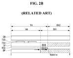
- FIG. 2B is a cross-sectional view schematically showing a cross section of FIG. 1 .
- a related art display device with a touch screen panel includes a display panel DP, a touch screen panel TP disposed on the display panel DP, and a cover window CW attached to the touch screen panel TP using an optically clear adhesive.
- the display panel DP includes an active area AA, on which information is displayed, and a first light shielding area BA1 positioned outside the active area AA.
- Display elements may be disposed in the active area AA, and lines used to supply various signals to the display elements and a display driver may be disposed in the first light shielding area BA1.
- the display panel DP may use a panel of a flat panel display, such as a liquid crystal display (LCD), an organic light emitting diode (OLED) display, a field emission display (FED), a plasma display panel (PDP), and electrophoresis display (EPD).
- LCD liquid crystal display
- OLED organic light emitting diode
- FED field emission display
- PDP plasma display panel
- EPD electrophoresis display
- the touch screen panel TP includes a touch area TA and a second light shielding area BA2 positioned outside the touch area TA.
- the touch area TA includes first touch electrodes TS1 to TS5 and second touch electrodes RS1 to RS6 which are disposed to cross each other.
- the second light shielding area BA2 includes first and second routing wires TW1 to TW5 and RW1 to RW6 for transmitting and receiving signals to and from the first and second touch electrodes TS 1 to TS5 and RS1 to RS6.
- the second light shielding area BA2 includes also first and second touch pads TP 1 to TP5 and RP 1 to RP6 which are connected to the first and second routing wires TW1 to TW5 and RW1 to RW6 and transmit and receive signals to and from the outside.
- bubbles may be generated in a contact portion of the display panel DP and the touch screen panel TP.
- FIG. 2B when the bubbles are generated in the contact portion, light generated in the active area AA of the display panel DP may be leaked into the first light shielding area BA1 of the display panel DP and may be upwardly emitted from an end of the touch area TA of the touch screen panel TP. If the bubble is not generated, the light may be shielded by the first light shielding area BA1 of the display panel DP.
- the related art display device with the touch screen panel leaks light into the light shielding area, which has to shield light, a boundary between the active area AA, on which information is displayed, and the first light shielding area BA1, on which the information is not displayed, is not clear and is blurred. As a result, the related art display device with the touch screen panel had a problem of bad display quality.
- the present disclosure provides a display device with a panel preventing light generated in a display panel from being leaked into a shielding area even when bubbles are generated in a contact portion of the display panel and a panel due to a bad adhesion.
- a display device with a panel comprising a display panel including an active area, on which information is displayed, and a first light shielding area positioned outside the active area and a panel disposed on the display panel, the panel including a first panel area having a size wider than the active area, a second light shielding area positioned outside the first panel area, and a third light shielding area ranging from a start position of the first light shielding area to a start position of the second light shielding area, wherein at least one dummy pattern is disposed in the third light shielding area of the panel.
- the at least one dummy pattern may include a first dummy pattern disposed in the third light shielding area on one surface of the panel.
- the at least one dummy pattern may include a second dummy pattern disposed in the third light shielding area on another surface of the panel.
- the panel has an upper surface and a lower surface, wherein the lower surface faces the display panel.
- the at least one dummy pattern may be disposed on one of the upper surface and the lower surface of the panel.
- the at least one dummy pattern may comprise a first dummy pattern and a second dummy pattern.
- the first dummy pattern may be on the lower surface of the panel.
- the second dummy pattern may be on an upper surface of the panel.
- the first dummy pattern and the second dummy pattern may be disposed to at least partially overlap each other. At least one of the first dummy pattern and the second dummy pattern may comprise a pattern with a plurality of unconnected areas.
- the first dummy pattern may be disposed in the third light shielding area as a continuous area, the second dummy pattern disposed in the third light shielding area as a pattern with a plurality of unconnected areas, with the second dummy pattern overlapping the first dummy pattern.
- the first and second dummy pattern may be disposed in the third light shielding are, the first and second dummy pattern are disposed as pattern with a plurality of unconnected areas, and the first dummy pattern and the second dummy pattern are disposed so that their respective areas are alternately disposed.
- the second dummy pattern may be disposed in the third light shielding area as a continuous area, the first dummy pattern is disposed in the third light shielding area as a pattern with a plurality of unconnected areas, and the first dummy pattern overlaps the second dummy pattern.
- the panel is a touch screen panel and the first panel area is a touch area.
- the display device with a touch screen panel may comprise a display panel including an active area, on which information is displayed, and a first light shielding area positioned adjacent to and outside of the active area.
- the touch screen panel overlaps the active area.
- the touch screen panel may at least partially overlap the active area.
- the touch screen panel includes a touch area having a size wider than the active area.
- the touch screen panel may include a touch area that extends beyond the active area.
- the second light shielding area may be positioned adjacent to and outside of the touch area.
- the third light shielding area may be considered to be positioned in the area that extends beyond the active area.
- the third light shielding area may overlap the first light shielding area.
- the third light shielding area may overlap the first light shielding area that neighbours the active area.
- the third light shielding area may not be overlapped by the second light shielding area.
- the third light shielding area may be positioned in a plane between the plane of the first light shielding area and the second light shielding area.
- the display device with the touch screen panel disposes the dummy pattern in the third light shielding area of the touch screen panel, in which the first light shielding area of the display panel and the second light shielding area of the touch screen panel do not overlap each other, thereby preventing a light leakage resulting from a bubble, which may be generated in a contact portion of the display panel and the touch screen panel, and improving display quality.
- some bubbles may be formed when laminating adhesive layers with a substrate.
- the term adjacent may be considered to mean next to and in contact with. Thus if one member is adjacent to another the members are side by side, for example, in relation to the first light shielding area and the active area.
- a display device with a touch screen panel according to a first embodiment of the invention is described with reference to FIGS. 3 to 5 .
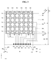
- FIG. 3 is a plan view of a display device with a touch screen panel according to a first embodiment of the invention.
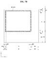
- FIG. 4A is a plan view schematically showing an example of a dummy pattern disposed in a third light shielding area shown in FIG. 3
- FIG. 4B is a plan view schematically showing another example of a dummy pattern disposed in a third light shielding area shown in FIG. 3 .
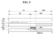
- FIG. 5 is a cross-sectional view schematically showing a portion of FIG. 3 .
- a dummy pattern may be considered to be any pattern of opaque material that is configured to shield light.
- the shielded light may be light that has been diffuse-reflected by one or more bubbles.
- a dummy pattern may function to prevent light from reaching the viewers of the display device through the bubbles.
- the dummy pattern may comprise a metal material.
- the metal material may comprise at least one of Cu, APC (Ag+Pd+Cu), and NiCr.
- a display device with a touch screen panel includes a display panel DP, a touch screen panel TP disposed on the display panel DP, and a cover window CW attached to the touch screen panel TP using an adhesive, for example, an optically clear adhesive.
- the display panel DP includes an active area AA, on which information is displayed, and a first light shielding area BA1 positioned outside the active area AA.
- Display elements may be disposed in the active area AA, and lines used to supply various signals to the display elements and a display driver may be disposed in the first light shielding area BA1.
- the display panel DP may use a panel of a flat panel display, such as a liquid crystal display (LCD), an organic light emitting diode (OLED) display, a field emission display (FED), a plasma display panel (PDP), and electrophoresis display (EPD).
- LCD liquid crystal display
- OLED organic light emitting diode
- FED field emission display
- PDP plasma display panel
- EPD electrophoresis display
- the touch screen panel TP includes a touch area TA, a second light shielding area BA2, and a third light shielding area BA3.
- the touch area TA includes first touch electrodes TS1 to TS5 and second touch electrodes RS1 to RS6 which are disposed to cross each other.
- the first touch electrodes TS1 to TS5 may be formed, or located, on one surface of the touch screen panel TP, and the second touch electrodes RS1 to RS6 may be formed, or located, on the other surface of the touch screen panel TP.
- the first touch electrodes TS1 to TS5 and the second touch electrodes RS1 to RS6 may be formed, or located, on one of both surfaces of the touch screen panel TP.
- an insulating pattern is disposed at crossings of the first touch electrodes TS 1 to TS5 and the second touch electrodes RS1 to RS6 and prevents the first touch electrodes TS 1 to TS5 and the second touch electrodes RS1 to RS6 from contacting each other.
- the second light shielding area BA2 is positioned outside the touch area TA.
- the second light shielding area BA2 includes first and second routing wires TW1 to TW5 and RW1 to RW6 for transmitting and receiving signals to and from the first and second touch electrodes TS1 to TS5 and RS1 to RS6 and first and second touch pads TP1 1 to TP5 and RP1 to RP6 which are connected to the first and second routing wires TW1 to TW5 and RW1 to RW6 and transmit and receive signals to and from the outside.
- the third light shielding area BA3 is an area ranging from a start position of the first light shielding area BA1 of the display panel DP to a start position of the second light shielding area BA2 of the touch screen panel TP.
- At least one first dummy pattern BP1 is disposed on one of an upper surface and a lower surface of the third light shielding area BA3 of the touch screen panel TP and surrounds the active area AA of the display panel DP.
- the first dummy pattern BP1 surrounding the active area AA may be disposed as one pattern in the third light shielding area BA3 on one surface of the touch screen panel TP, or may be divided into a plurality of patterns BP1.
- a plurality of patterns may be considered to be a pattern comprising a plurality of unconnected areas. In other words a pattern comprising a plurality of isolated shapes.
- one pattern may be considered to be a continuous area.
- the first dummy pattern BP1 may include a light shielding material capable of shielding light.
- the display device with the touch screen panel according to the first embodiment of the invention disposes the dummy pattern BP1 in the third light shielding area BA3 of the touch screen panel TP, in which the first light shielding area BA1 of the display panel DP and the second light shielding area BA2 of the touch screen panel TP do not overlap each other, thereby preventing a light leakage resulting from a bubble, which may be generated in a contact portion of the display panel DP and the touch screen panel TP.
- the invention can obtain an improvement in display quality.
- the display device with the touch screen panel according to the first embodiment of the invention when the first dummy pattern BP1 is formed in a plurality of patterns, a small amount of light may be leaked between the plurality of patterns.
- a display device with a touch screen panel according to a second embodiment of the invention is configured such that leaked light is more completely shielded than through a first dummy pattern.
- FIGS. 6 to 8 a display device with a touch screen panel according to a second embodiment of the invention is described with reference to FIGS. 6 to 8 .
- FIG. 6 is a plan view of a display device with a touch screen panel according to a second embodiment of the invention.
- FIG. 7A is a plan view schematically showing an example of a dummy pattern disposed in a third light shielding area shown in FIG. 6
- FIG. 7B is a plan view schematically showing another example of a dummy pattern disposed in a third light shielding area shown in FIG. 6 .
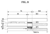
- FIG. 8 is a cross-sectional view schematically showing a portion of FIG. 6 .
- a display device with a touch screen panel includes a display panel DP, a touch screen panel TP disposed on the display panel DP, and a cover window CW attached to the touch screen panel TP using an adhesive, for example, an optically clear adhesive.
- the display panel DP includes an active area AA, on which information is displayed, and a first light shielding area BA1 positioned outside the active area AA.
- Display elements may be disposed in the active area AA, and lines used to supply various signals to the display elements and a display driver may be disposed in the first light shielding area BA1.
- the display panel DP may use a panel of a flat panel display, such as a liquid crystal display (LCD), an organic light emitting diode (OLED) display, a field emission display (FED), a plasma display panel (PDP), and electrophoresis display (EPD).
- LCD liquid crystal display
- OLED organic light emitting diode
- FED field emission display
- PDP plasma display panel
- EPD electrophoresis display
- the touch screen panel TP includes a touch area TA, a second light shielding area BA2, and a third light shielding area BA3.
- the touch area TA includes first touch electrodes TS1 to TS5 and second touch electrodes RS1 to RS6 which are disposed to cross each other.
- the first touch electrodes TS1 to TS5 may be formed, or located, on one surface of the touch screen panel TP, and the second touch electrodes RS1 to RS6 may be formed, or located, on the other surface of the touch screen panel TP.
- the first touch electrodes TS1 to TS5 and the second touch electrodes RS1 to RS6 may be formed, or located, on one of both surfaces of the touch screen panel TP.
- an insulating pattern is disposed at crossings of the first touch electrodes TS1 to TS5 and the second touch electrodes RS1 to RS6 and prevents the first touch electrodes TS1 to TS5 and the second touch electrodes RS1 to RS6 from contacting each other.
- the second light shielding area BA2 is positioned outside the touch area TA.
- the second light shielding area BA2 includes first and second routing wires TW1 to TW5 and RW1 to RW6 for transmitting and receiving signals to and from the first and second touch electrodes TS1 to TS5 and RS1 to RS6 and first and second touch pads TP1 to TP5 and RP1 to RP6 which are connected to the first and second routing wires TW1 to TW5 and RW1 to RW6 and transmit and receive signals to and from the outside.
- the third light shielding area BA3 is an area ranging from a start position of the first light shielding area BA1 of the display panel DP to a start position of the second light shielding area BA2 of the touch screen panel TP.
- At least one first dummy pattern BP1 is disposed on a lower surface of the third light shielding area BA3 of the touch screen panel TP and surrounds the active area AA of the display panel DP.
- the first dummy pattern BP1 surrounding the active area AA may be disposed as one pattern in the third light shielding area BA3 on the lower surface of the touch screen panel TP, or may be divided into a plurality of patterns.
- At least one second dummy pattern BP2 is disposed on an upper surface of the third light shielding area BA3 of the touch screen panel TP and surrounds the active area AA of the display panel DP.
- the second dummy pattern BP2 surrounding the active area AA may be disposed as one pattern in the third light shielding area BA3 on the upper surface of the touch screen panel TP, or the second dummy pattern BP2 may be divided into a plurality of patterns BP2.
- the first dummy pattern BP1 and the second dummy pattern BP2 may include a light shielding material capable of shielding light.
- One of the first dummy pattern BP1 and the second dummy pattern BP2 may be formed as one pattern, and the other may be formed as a plurality of patterns. Both the first dummy pattern BP1 and the second dummy pattern BP2 may be formed as one pattern or a plurality of patterns.
- the first dummy pattern BP1 and the second dummy pattern BP2 may overlap each other.
- the first dummy pattern BP1 and the second dummy pattern BP2 may be alternately disposed. In this instance, when the first dummy pattern BP1 and the second dummy pattern BP2 are disposed to partially overlap each other, a leakage of light may be shielded more certainly.
- the display device with the touch screen panel according to the second embodiment of the invention disposes the first and second dummy patterns BP1 and BP2 on the upper and lower surfaces of the third light shielding area BA3 of the touch screen panel TP, in which the first light shielding area BA1 of the display panel DP and the second light shielding area BA2 of the touch screen panel TP do not overlap each other, thereby preventing a light leakage resulting from a bubble, which may be generated in a contact portion of the display panel DP and the touch screen panel TP, more efficiently than the first embodiment of the invention.
- the second embodiment of the invention can obtain an improvement in display quality.
- the touch screen panel and the display panel have a rectangular shape.
- the touch screen panel and the display panel may have a circle, an oval, a triangle, and a polygon, etc.
- the touch screen panel according to the embodiments of the invention is applied to the OLED display, the touch screen panel can be interpreted to include a barrier layer or an encapsulation layer.
Landscapes
- Engineering & Computer Science (AREA)
- Physics & Mathematics (AREA)
- Theoretical Computer Science (AREA)
- General Engineering & Computer Science (AREA)
- General Physics & Mathematics (AREA)
- Nonlinear Science (AREA)
- Human Computer Interaction (AREA)
- Crystallography & Structural Chemistry (AREA)
- Optics & Photonics (AREA)
- Chemical & Material Sciences (AREA)
- Mathematical Physics (AREA)
- Microelectronics & Electronic Packaging (AREA)
- Devices For Indicating Variable Information By Combining Individual Elements (AREA)
- Liquid Crystal (AREA)
- Position Input By Displaying (AREA)
Abstract
Description
- The present disclosure relates to a display device with a touch screen panel, and more particularly to a display device with a touch screen panel for preventing a light leakage from being generated in a touch area due to a coupling of the touch screen panel and the display device.
- In recent years, various input devices, such as a keyboard, a mouse, a track ball, a joystick, and a digitizer, have been used to allow users to interface with home appliances or information telecommunication devices. However, when the user makes use of these input devices, user's dissatisfaction increases because the user is required to learn how to use the input devices and the input devices occupy space. Thus, a demand for a convenient and simple input device capable of reducing erroneous operations is increasing. In response to the demand, a touch screen panel was proposed to recognize information when the user inputs the information by directly touching the screen with his or her hand or a pen.
- Touch screen panels are classified into a resistive type, a capacitive type, an electromagnetic type, etc. based on a method for sensing a touched portion. The resistive touch screen panel determines a touched position by a voltage gradient based on changes of resistance in a state where a DC voltage is applied to metal electrodes formed, or located, on an upper plate or a lower plate. The capacitive touch screen panel senses a touched position based on changes in capacitance generated in an upper plate or a lower plate when the user touches an equipotential conductive film formed, or located, on the upper or lower plate. The electromagnetic touch screen panel senses a touched portion by reading an LC value induced when an electronic pen touches a conductive film. In addition, an optical touch screen panel, an ultrasonic touch screen panel, etc. are known.
- The capacitive touch screen panel may be subdivided into a self-capacitive touch screen panel and a mutual capacitive touch screen panel. The self-capacitive touch screen panel forms a plurality of independent patterns in a touch area of the touch screen panel and measures changes in a capacitance of each independent pattern, thereby determining whether or not a touch operation is performed. The mutual capacitive touch screen panel crosses X-axis electrode lines (for example, driving electrode lines) and Y-axis electrode lines (for example, sensing electrode lines) in a touch electrode formation area of the touch screen panel to form a matrix, applies a driving pulse to the X-axis electrode lines, and senses changes in voltages generated in sensing nodes defined as crossings of the X-axis electrode lines and the Y-axis electrode lines through the Y-axis electrode lines, thereby determining whether or not a touch operation is performed.
- A related art display device (hereinafter simply referred to as "a display device with a touch screen panel") including a capacitive touch screen panel is described below with reference to
FIGS. 1 to 2B . -
FIG. 1 is a plan view of a related art display device with a touch screen panel.FIG. 2A is a plan view schematically showing an active area, a touch area, and a visible area ofFIG. 1 , andFIG. 2B is a cross-sectional view schematically showing a cross section ofFIG. 1 . - Referring to
FIGS. 1 to 2B , a related art display device with a touch screen panel includes a display panel DP, a touch screen panel TP disposed on the display panel DP, and a cover window CW attached to the touch screen panel TP using an optically clear adhesive. - The display panel DP includes an active area AA, on which information is displayed, and a first light shielding area BA1 positioned outside the active area AA. Display elements may be disposed in the active area AA, and lines used to supply various signals to the display elements and a display driver may be disposed in the first light shielding area BA1. The display panel DP may use a panel of a flat panel display, such as a liquid crystal display (LCD), an organic light emitting diode (OLED) display, a field emission display (FED), a plasma display panel (PDP), and electrophoresis display (EPD).
- The touch screen panel TP includes a touch area TA and a second light shielding area BA2 positioned outside the touch area TA. The touch area TA includes first touch electrodes TS1 to TS5 and second touch electrodes RS1 to RS6 which are disposed to cross each other. The second light shielding area BA2 includes first and second routing wires TW1 to TW5 and RW1 to RW6 for transmitting and receiving signals to and from the first and second
touch electrodes TS 1 to TS5 and RS1 to RS6. The second light shielding area BA2 includes also first and secondtouch pads TP 1 to TP5 andRP 1 to RP6 which are connected to the first and second routing wires TW1 to TW5 and RW1 to RW6 and transmit and receive signals to and from the outside. - In the related art display device with the touch screen panel, bubbles may be generated in a contact portion of the display panel DP and the touch screen panel TP. As shown in
FIG. 2B , when the bubbles are generated in the contact portion, light generated in the active area AA of the display panel DP may be leaked into the first light shielding area BA1 of the display panel DP and may be upwardly emitted from an end of the touch area TA of the touch screen panel TP. If the bubble is not generated, the light may be shielded by the first light shielding area BA1 of the display panel DP. However, when the bubbles are generated due to a bad adhesion, etc., the light leaked into the first light shielding area BA1 may be upwardly emitted from the end of the touch area TA through the bubbles. Thus, because the related art display device with the touch screen panel leaks light into the light shielding area, which has to shield light, a boundary between the active area AA, on which information is displayed, and the first light shielding area BA1, on which the information is not displayed, is not clear and is blurred. As a result, the related art display device with the touch screen panel had a problem of bad display quality. - The present disclosure provides a display device with a panel preventing light generated in a display panel from being leaked into a shielding area even when bubbles are generated in a contact portion of the display panel and a panel due to a bad adhesion.
- In one aspect, there is provided a display device with a panel comprising a display panel including an active area, on which information is displayed, and a first light shielding area positioned outside the active area and a panel disposed on the display panel, the panel including a first panel area having a size wider than the active area, a second light shielding area positioned outside the first panel area, and a third light shielding area ranging from a start position of the first light shielding area to a start position of the second light shielding area, wherein at least one dummy pattern is disposed in the third light shielding area of the panel.
- The at least one dummy pattern may include a first dummy pattern disposed in the third light shielding area on one surface of the panel.
- The at least one dummy pattern may include a second dummy pattern disposed in the third light shielding area on another surface of the panel.
- The panel has an upper surface and a lower surface, wherein the lower surface faces the display panel.
- The at least one dummy pattern may be disposed on one of the upper surface and the lower surface of the panel.
- The at least one dummy pattern may comprise a first dummy pattern and a second dummy pattern. The first dummy pattern may be on the lower surface of the panel. The second dummy pattern may be on an upper surface of the panel.
- The first dummy pattern and the second dummy pattern may be disposed to at least partially overlap each other. At least one of the first dummy pattern and the second dummy pattern may comprise a pattern with a plurality of unconnected areas.
- The first dummy pattern may be disposed in the third light shielding area as a continuous area, the second dummy pattern disposed in the third light shielding area as a pattern with a plurality of unconnected areas, with the second dummy pattern overlapping the first dummy pattern.
- Optionally, the first and second dummy pattern may be disposed in the third light shielding are, the first and second dummy pattern are disposed as pattern with a plurality of unconnected areas, and the first dummy pattern and the second dummy pattern are disposed so that their respective areas are alternately disposed.
- Optionally, the second dummy pattern may be disposed in the third light shielding area as a continuous area, the first dummy pattern is disposed in the third light shielding area as a pattern with a plurality of unconnected areas, and the first dummy pattern overlaps the second dummy pattern.
- Preferably, the panel is a touch screen panel and the first panel area is a touch area.
- The display device with a touch screen panel may comprise a display panel including an active area, on which information is displayed, and a first light shielding area positioned adjacent to and outside of the active area. The touch screen panel overlaps the active area. In particular, the touch screen panel may at least partially overlap the active area. As noted above, the touch screen panel includes a touch area having a size wider than the active area. In other words, the touch screen panel may include a touch area that extends beyond the active area. The second light shielding area may be positioned adjacent to and outside of the touch area.
- The third light shielding area may be considered to be positioned in the area that extends beyond the active area. The third light shielding area may overlap the first light shielding area. In particular, the third light shielding area may overlap the first light shielding area that neighbours the active area. In turn, the third light shielding area may not be overlapped by the second light shielding area. Overall, the third light shielding area may be positioned in a plane between the plane of the first light shielding area and the second light shielding area.
- The display device with the touch screen panel according to the present disclosure disposes the dummy pattern in the third light shielding area of the touch screen panel, in which the first light shielding area of the display panel and the second light shielding area of the touch screen panel do not overlap each other, thereby preventing a light leakage resulting from a bubble, which may be generated in a contact portion of the display panel and the touch screen panel, and improving display quality.
- The accompanying drawings, which are included to provide a further understanding of the invention and are incorporated in and constitute a part of this specification, illustrate embodiments of the invention and together with the description serve to explain the principles of the invention. In the drawings:
-
FIG. 1 is a plan view of a related art display device with a touch screen panel; -
FIG. 2A is a plan view schematically showing an active area, a first light shielding area, and a second light shielding area ofFIG. 1 ; -
FIG. 2B is a cross-sectional view schematically showing a cross section ofFIG. 1 ; -
FIG. 3 is a plan view of a display device with a touch screen panel according to a first embodiment of the invention; -
FIG. 4A is a plan view schematically showing an example of a dummy pattern disposed in a third light shielding area shown inFIG. 3 ; -
FIG. 4B is a plan view schematically showing another example of a dummy pattern disposed in a third light shielding area shown inFIG. 3 ; -
FIG. 5 is a cross-sectional view schematically showing a portion ofFIG. 3 ; -
FIG. 6 is a plan view of a display device with a touch screen panel according to a second embodiment of the invention; -
FIG. 7A is a plan view schematically showing an example of a dummy pattern disposed in a third light shielding area shown inFIG. 6 ; -
FIG. 7B is a plan view schematically showing another example of a dummy pattern disposed in a third light shielding area shown inFIG. 6 ; and -
FIG. 8 is a cross-sectional view schematically showing a portion ofFIG. 6 . - Reference will now be made in detail to embodiments of the invention, examples of which are illustrated in the accompanying drawings. Wherever possible, the same reference numbers will be used throughout the drawings to refer to the same or like parts. Detailed description of known arts will be omitted if it is determined that the arts can mislead the reader regarding the embodiments of the invention. Names of components used in the following description may be selected in consideration of facility of specification preparation. Thus, the names of the components may be different from names of components used in real products. Many defects appear to the user of display devices as bubbles in the device. For example, a void or gap between two components in a display device may be called a bubble. Accordingly, the term bubble may be used to describe such defects. As an example, some bubbles may be formed when laminating adhesive layers with a substrate. The term adjacent may be considered to mean next to and in contact with. Thus if one member is adjacent to another the members are side by side, for example, in relation to the first light shielding area and the active area.
- A display device with a touch screen panel according to a first embodiment of the invention is described with reference to
FIGS. 3 to 5 . -
FIG. 3 is a plan view of a display device with a touch screen panel according to a first embodiment of the invention.FIG. 4A is a plan view schematically showing an example of a dummy pattern disposed in a third light shielding area shown inFIG. 3 , andFIG. 4B is a plan view schematically showing another example of a dummy pattern disposed in a third light shielding area shown inFIG. 3 .FIG. 5 is a cross-sectional view schematically showing a portion ofFIG. 3 . A dummy pattern may be considered to be any pattern of opaque material that is configured to shield light. The shielded light may be light that has been diffuse-reflected by one or more bubbles. As an example, a dummy pattern may function to prevent light from reaching the viewers of the display device through the bubbles. The dummy pattern may comprise a metal material. The metal material may comprise at least one of Cu, APC (Ag+Pd+Cu), and NiCr. - Referring to
FIGS. 3 to 5 , a display device with a touch screen panel according to a first embodiment of the invention includes a display panel DP, a touch screen panel TP disposed on the display panel DP, and a cover window CW attached to the touch screen panel TP using an adhesive, for example, an optically clear adhesive. - The display panel DP includes an active area AA, on which information is displayed, and a first light shielding area BA1 positioned outside the active area AA. Display elements may be disposed in the active area AA, and lines used to supply various signals to the display elements and a display driver may be disposed in the first light shielding area BA1. The display panel DP may use a panel of a flat panel display, such as a liquid crystal display (LCD), an organic light emitting diode (OLED) display, a field emission display (FED), a plasma display panel (PDP), and electrophoresis display (EPD).
- The touch screen panel TP includes a touch area TA, a second light shielding area BA2, and a third light shielding area BA3.
- The touch area TA includes first touch electrodes TS1 to TS5 and second touch electrodes RS1 to RS6 which are disposed to cross each other.
- The first touch electrodes TS1 to TS5 may be formed, or located, on one surface of the touch screen panel TP, and the second touch electrodes RS1 to RS6 may be formed, or located, on the other surface of the touch screen panel TP. The first touch electrodes TS1 to TS5 and the second touch electrodes RS1 to RS6 may be formed, or located, on one of both surfaces of the touch screen panel TP. In this instance, an insulating pattern is disposed at crossings of the first
touch electrodes TS 1 to TS5 and the second touch electrodes RS1 to RS6 and prevents the firsttouch electrodes TS 1 to TS5 and the second touch electrodes RS1 to RS6 from contacting each other. - The second light shielding area BA2 is positioned outside the touch area TA. The second light shielding area BA2 includes first and second routing wires TW1 to TW5 and RW1 to RW6 for transmitting and receiving signals to and from the first and second touch electrodes TS1 to TS5 and RS1 to RS6 and first and second
touch pads TP1 1 to TP5 and RP1 to RP6 which are connected to the first and second routing wires TW1 to TW5 and RW1 to RW6 and transmit and receive signals to and from the outside.
The third light shielding area BA3 is an area ranging from a start position of the first light shielding area BA1 of the display panel DP to a start position of the second light shielding area BA2 of the touch screen panel TP. At least one first dummy pattern BP1 is disposed on one of an upper surface and a lower surface of the third light shielding area BA3 of the touch screen panel TP and surrounds the active area AA of the display panel DP. For example, the first dummy pattern BP1 surrounding the active area AA may be disposed as one pattern in the third light shielding area BA3 on one surface of the touch screen panel TP, or may be divided into a plurality of patterns BP1. A plurality of patterns may be considered to be a pattern comprising a plurality of unconnected areas. In other words a pattern comprising a plurality of isolated shapes. Relatedly, one pattern may be considered to be a continuous area. - The first dummy pattern BP1 may include a light shielding material capable of shielding light.
- Accordingly, the display device with the touch screen panel according to the first embodiment of the invention disposes the dummy pattern BP1 in the third light shielding area BA3 of the touch screen panel TP, in which the first light shielding area BA1 of the display panel DP and the second light shielding area BA2 of the touch screen panel TP do not overlap each other, thereby preventing a light leakage resulting from a bubble, which may be generated in a contact portion of the display panel DP and the touch screen panel TP. Hence, the invention can obtain an improvement in display quality.
- However, in the display device with the touch screen panel according to the first embodiment of the invention, when the first dummy pattern BP1 is formed in a plurality of patterns, a small amount of light may be leaked between the plurality of patterns.
- A display device with a touch screen panel according to a second embodiment of the invention is configured such that leaked light is more completely shielded than through a first dummy pattern.
- Next, a display device with a touch screen panel according to a second embodiment of the invention is described with reference to
FIGS. 6 to 8 . -
FIG. 6 is a plan view of a display device with a touch screen panel according to a second embodiment of the invention.FIG. 7A is a plan view schematically showing an example of a dummy pattern disposed in a third light shielding area shown inFIG. 6 , andFIG. 7B is a plan view schematically showing another example of a dummy pattern disposed in a third light shielding area shown inFIG. 6 .FIG. 8 is a cross-sectional view schematically showing a portion ofFIG. 6 . - Referring to
FIGS. 6 to 8 , a display device with a touch screen panel according to a second embodiment of the invention includes a display panel DP, a touch screen panel TP disposed on the display panel DP, and a cover window CW attached to the touch screen panel TP using an adhesive, for example, an optically clear adhesive. - The display panel DP includes an active area AA, on which information is displayed, and a first light shielding area BA1 positioned outside the active area AA. Display elements may be disposed in the active area AA, and lines used to supply various signals to the display elements and a display driver may be disposed in the first light shielding area BA1. The display panel DP may use a panel of a flat panel display, such as a liquid crystal display (LCD), an organic light emitting diode (OLED) display, a field emission display (FED), a plasma display panel (PDP), and electrophoresis display (EPD).
- The touch screen panel TP includes a touch area TA, a second light shielding area BA2, and a third light shielding area BA3.
- The touch area TA includes first touch electrodes TS1 to TS5 and second touch electrodes RS1 to RS6 which are disposed to cross each other.
- The first touch electrodes TS1 to TS5 may be formed, or located, on one surface of the touch screen panel TP, and the second touch electrodes RS1 to RS6 may be formed, or located, on the other surface of the touch screen panel TP. The first touch electrodes TS1 to TS5 and the second touch electrodes RS1 to RS6 may be formed, or located, on one of both surfaces of the touch screen panel TP. In this instance, an insulating pattern is disposed at crossings of the first touch electrodes TS1 to TS5 and the second touch electrodes RS1 to RS6 and prevents the first touch electrodes TS1 to TS5 and the second touch electrodes RS1 to RS6 from contacting each other.
- The second light shielding area BA2 is positioned outside the touch area TA. The second light shielding area BA2 includes first and second routing wires TW1 to TW5 and RW1 to RW6 for transmitting and receiving signals to and from the first and second touch electrodes TS1 to TS5 and RS1 to RS6 and first and second touch pads TP1 to TP5 and RP1 to RP6 which are connected to the first and second routing wires TW1 to TW5 and RW1 to RW6 and transmit and receive signals to and from the outside.
- The third light shielding area BA3 is an area ranging from a start position of the first light shielding area BA1 of the display panel DP to a start position of the second light shielding area BA2 of the touch screen panel TP.
- At least one first dummy pattern BP1 is disposed on a lower surface of the third light shielding area BA3 of the touch screen panel TP and surrounds the active area AA of the display panel DP. For example, the first dummy pattern BP1 surrounding the active area AA may be disposed as one pattern in the third light shielding area BA3 on the lower surface of the touch screen panel TP, or may be divided into a plurality of patterns.
- Further, at least one second dummy pattern BP2 is disposed on an upper surface of the third light shielding area BA3 of the touch screen panel TP and surrounds the active area AA of the display panel DP. For example, the second dummy pattern BP2 surrounding the active area AA may be disposed as one pattern in the third light shielding area BA3 on the upper surface of the touch screen panel TP, or the second dummy pattern BP2 may be divided into a plurality of patterns BP2.
- The first dummy pattern BP1 and the second dummy pattern BP2 may include a light shielding material capable of shielding light.
- One of the first dummy pattern BP1 and the second dummy pattern BP2 may be formed as one pattern, and the other may be formed as a plurality of patterns. Both the first dummy pattern BP1 and the second dummy pattern BP2 may be formed as one pattern or a plurality of patterns.
- When the first dummy pattern BP1 and the second dummy pattern BP2 are disposed in the third light shielding area BA3 as one pattern, the first dummy pattern BP1 and the second dummy pattern BP2 may overlap each other. When the first dummy pattern BP1 and the second dummy pattern BP2 are disposed in the third light shielding area BA3 as a plurality of patterns, the first dummy pattern BP1 and the second dummy pattern BP2 may be alternately disposed. In this instance, when the first dummy pattern BP1 and the second dummy pattern BP2 are disposed to partially overlap each other, a leakage of light may be shielded more certainly.
- The display device with the touch screen panel according to the second embodiment of the invention disposes the first and second dummy patterns BP1 and BP2 on the upper and lower surfaces of the third light shielding area BA3 of the touch screen panel TP, in which the first light shielding area BA1 of the display panel DP and the second light shielding area BA2 of the touch screen panel TP do not overlap each other, thereby preventing a light leakage resulting from a bubble, which may be generated in a contact portion of the display panel DP and the touch screen panel TP, more efficiently than the first embodiment of the invention. Hence, the second embodiment of the invention can obtain an improvement in display quality.
- Although embodiments have been described with reference to a number of illustrative embodiments thereof, it should be understood that numerous other modifications and embodiments can be devised by those skilled in the art that will fall within the scope of the principles of this disclosure. For example, the embodiments of the invention described and illustrated that the touch screen panel and the display panel have a rectangular shape. However, the touch screen panel and the display panel may have a circle, an oval, a triangle, and a polygon, etc. Further, when the touch screen panel according to the embodiments of the invention is applied to the OLED display, the touch screen panel can be interpreted to include a barrier layer or an encapsulation layer. Thus, various variations and modifications are possible in the component parts and/or arrangements of the subject combination arrangement within the scope of the appended claims.
- The following is a list of exemplary aspects of the present invention:
-
Aspect 1. A display device with a touch screen panel comprising:- a display panel including an active area, on which information is displayed, and a first light shielding area positioned outside the active area; and
- a touch screen panel disposed on the display panel, the touch screen panel including a touch area having a size wider than the active area, a second light shielding area positioned outside the touch area, and a third light shielding area ranging from a start position of the first light shielding area to a start position of the second light shielding area,
- wherein at least one dummy pattern is disposed in the third light shielding area of the touch screen panel.
-
Aspect 2. The display device with the touch screen panel ofaspect 1, wherein the at least one dummy pattern includes a first dummy pattern disposed in the third light shielding area on one surface of the touch screen panel. -
Aspect 3. The display device with the touch screen panel ofaspect 2, wherein the first dummy pattern is disposed in the third light shielding area as one pattern or a plurality of patterns. -
Aspect 4. The display device with the touch screen panel ofaspect 2, wherein the at least one dummy pattern includes a second dummy pattern disposed in the third light shielding area on another surface of the touch screen panel. -
Aspect 5. The display device with the touch screen panel ofaspect 3, wherein the at least one dummy pattern includes a second dummy pattern disposed in the third light shielding area on another surface of the touch screen panel. -
Aspect 6. The display device with the touch screen panel ofaspect 4, wherein the second dummy pattern is disposed in the third light shielding area as one pattern or a plurality of patterns. - Aspect 7. The display device with the touch screen panel of
aspect 5, wherein the second dummy pattern is disposed in the third light shielding area as one pattern or a plurality of patterns. - Aspect 8. The display device with the touch screen panel of
aspect 6, wherein when the first dummy pattern is disposed in the third light shielding area as one pattern and the second dummy pattern is disposed in the third light shielding area as the plurality of patterns, the second dummy patterns overlap the first dummy pattern. - Aspect 9. The display device with the touch screen panel of aspect 7, wherein when the first and second dummy patterns are disposed in the third light shielding area as the plurality of patterns, respectively, the first dummy pattern and the second dummy pattern are alternately disposed.
-
Aspect 10. The display device with the touch screen panel ofaspect 5, wherein when the second dummy pattern is disposed in the third light shielding area as one pattern and the first dummy patterns are disposed in the third light shielding area as the plurality of patterns, the first dummy patterns overlap the second dummy pattern.
Claims (12)
- A display device with a panel comprising:a display panel including an active area (AA), on which information is displayed, and a first light shielding area (BA1) positioned outside of the active area (AA); anda panel disposed on the display panel, the panel including a first panel area having a size wider than the active area (AA), a second light shielding area (BA2) positioned outside the first panel area, and a third light shielding area (BS3) ranging from a start position of the first light shielding area to a start position of the second light shielding area,wherein at least one dummy pattern (BP1,2) is disposed in the third light shielding area (BS3) of the panel.
- The display device of claim 1, wherein the at least one dummy pattern includes a first dummy pattern (BP1) disposed in the third light shielding area (BS3) on one surface of the panel.
- The display device of claim 2, wherein the at least one dummy pattern includes a second dummy pattern (BP2) disposed in the third light shielding area (BS3) on another surface of the panel.
- The display device according to any preceding claim, wherein the panel has an upper surface and a lower surface, wherein the lower surface faces the display panel, and the at least one dummy pattern is disposed on one of the upper surface and the lower surface of the panel.
- The display device according to any preceding claim, wherein the panel has an upper surface and a lower surface, wherein the lower surface faces the display panel, wherein the at least one dummy pattern comprises a first dummy pattern (BP1) disposed on the lower surface of the panel.
- The display device of claims 2, 3 or 5, wherein the at least one dummy pattern further comprises a second dummy pattern (BP2) disposed on the upper surface of the panel.
- The display device of claims 3 or 6, wherein the first dummy pattern (BP1) and the second dummy pattern (BP2) are disposed to at least partially overlap each other.
- The display device of claims 3, 6 or 7, wherein at least one of the first dummy pattern (BP1) and the second dummy pattern (BP2) comprises a pattern with a plurality of unconnected areas.
- The display device of claim 3 or claims 6 to 8, wherein the first dummy pattern (BP1) is disposed in the third light shielding area (BS3) as a continuous area, the second dummy pattern (BP2) is disposed in the third light shielding area (BS3) as a pattern with a plurality of unconnected areas, and the second dummy pattern (BP2) overlaps the first dummy pattern (BP1).
- The display device of claim 3 or claims 6 to 8, wherein the first (BP1) and second dummy pattern (BP2) are disposed in the third light shielding area (BS3), the first (BP1) and second dummy pattern (BP2) are disposed as patterns with a plurality of unconnected areas; and the first dummy pattern (BP1) and the second dummy pattern (BP2) are disposed so that their respective areas are alternately disposed.
- The display device of claim 3 or claims 6 to 8, wherein the second dummy pattern (BP2) is disposed in the third light shielding area (BS3) as a continuous area, the first dummy pattern (BP1) is disposed in the third light shielding area (BS3) as a pattern with a plurality of unconnected areas, and the first dummy pattern (BP1) overlaps the second dummy pattern (BP2).
- The display device of any one of the preceding claims, wherein the panel is a touch screen panel (TP) and the first panel area is a touch area (TA).
Applications Claiming Priority (1)
| Application Number | Priority Date | Filing Date | Title |
|---|---|---|---|
| KR1020150167478A KR102507338B1 (en) | 2015-11-27 | 2015-11-27 | Display device with touch screen panel |
Publications (2)
| Publication Number | Publication Date |
|---|---|
| EP3173910A1 true EP3173910A1 (en) | 2017-05-31 |
| EP3173910B1 EP3173910B1 (en) | 2018-03-21 |
Family
ID=57136798
Family Applications (1)
| Application Number | Title | Priority Date | Filing Date |
|---|---|---|---|
| EP16194030.9A Active EP3173910B1 (en) | 2015-11-27 | 2016-10-14 | Display device with touch screen panel |
Country Status (4)
| Country | Link |
|---|---|
| US (1) | US10416818B2 (en) |
| EP (1) | EP3173910B1 (en) |
| KR (1) | KR102507338B1 (en) |
| CN (1) | CN107037908B (en) |
Families Citing this family (1)
| Publication number | Priority date | Publication date | Assignee | Title |
|---|---|---|---|---|
| CN117280895B (en) * | 2022-04-21 | 2025-02-11 | 京东方科技集团股份有限公司 | Luminescent substrate and preparation method thereof, and luminescent device |
Citations (3)
| Publication number | Priority date | Publication date | Assignee | Title |
|---|---|---|---|---|
| US20130038542A1 (en) * | 2011-08-11 | 2013-02-14 | Lg Display Co., Ltd. | Display Device Integrated with Touch Panel |
| US20140225843A1 (en) * | 2013-02-08 | 2014-08-14 | Acer Incorporated | Touch panel |
| US20150114815A1 (en) * | 2013-10-26 | 2015-04-30 | Tpk Touch Systems (Xiamen) Inc. | Touch panel and method for manufacturing the same |
Family Cites Families (12)
| Publication number | Priority date | Publication date | Assignee | Title |
|---|---|---|---|---|
| CN100435013C (en) * | 1997-06-17 | 2008-11-19 | 精工爱普生株式会社 | Electro-optic device substrates, electro-optic devices, electronic devices and projection display equipment |
| TW353157B (en) * | 1998-06-25 | 1999-02-21 | United Microelectronics Corp | Double faced mask |
| JP5337061B2 (en) * | 2009-02-20 | 2013-11-06 | セイコーインスツル株式会社 | Touch panel and display device including the same |
| KR101048931B1 (en) * | 2010-04-01 | 2011-07-12 | 삼성모바일디스플레이주식회사 | Touch screen panel |
| KR101113467B1 (en) * | 2010-04-01 | 2012-02-29 | 삼성모바일디스플레이주식회사 | Touch Screen Panel |
| KR101785043B1 (en) | 2010-12-29 | 2017-10-13 | 엘지디스플레이 주식회사 | Touch type organic electro luminescent device |
| CN102955603B (en) * | 2011-08-17 | 2016-05-25 | 宸鸿科技(厦门)有限公司 | Contact panel and manufacture method thereof |
| JP6136184B2 (en) * | 2012-10-16 | 2017-05-31 | 大日本印刷株式会社 | Front protective plate for display device with wiring, and display device |
| CN104781764B (en) * | 2012-10-29 | 2017-07-18 | 夏普株式会社 | Touch panel |
| CN103336607A (en) * | 2013-06-14 | 2013-10-02 | 业成光电(深圳)有限公司 | Touch display panel |
| KR20150000383A (en) | 2013-06-24 | 2015-01-02 | (주)티메이 | Touch Screen Panel and Touch Screen Panel Assembly |
| KR102174088B1 (en) * | 2014-01-08 | 2020-11-05 | 삼성디스플레이 주식회사 | Display panel, method of manufacturing the display panel and display apparatus |
-
2015
- 2015-11-27 KR KR1020150167478A patent/KR102507338B1/en active Active
-
2016
- 2016-10-14 EP EP16194030.9A patent/EP3173910B1/en active Active
- 2016-11-10 US US15/348,519 patent/US10416818B2/en active Active
- 2016-11-15 CN CN201611004912.1A patent/CN107037908B/en active Active
Patent Citations (3)
| Publication number | Priority date | Publication date | Assignee | Title |
|---|---|---|---|---|
| US20130038542A1 (en) * | 2011-08-11 | 2013-02-14 | Lg Display Co., Ltd. | Display Device Integrated with Touch Panel |
| US20140225843A1 (en) * | 2013-02-08 | 2014-08-14 | Acer Incorporated | Touch panel |
| US20150114815A1 (en) * | 2013-10-26 | 2015-04-30 | Tpk Touch Systems (Xiamen) Inc. | Touch panel and method for manufacturing the same |
Also Published As
| Publication number | Publication date |
|---|---|
| CN107037908A (en) | 2017-08-11 |
| KR20170062602A (en) | 2017-06-08 |
| US10416818B2 (en) | 2019-09-17 |
| KR102507338B1 (en) | 2023-03-08 |
| CN107037908B (en) | 2020-04-28 |
| EP3173910B1 (en) | 2018-03-21 |
| US20170153729A1 (en) | 2017-06-01 |
Similar Documents
| Publication | Publication Date | Title |
|---|---|---|
| JP5563417B2 (en) | Display device with touch panel | |
| CN107545235B (en) | display device | |
| CN107179847B (en) | Detection devices, display devices and electronic equipment | |
| KR100628265B1 (en) | Resistive Touch Panel | |
| KR100837738B1 (en) | Electronic device and touch panel placement method | |
| KR101868473B1 (en) | Display Device Integrated with Touch Screen | |
| US9395854B2 (en) | Touch sensing panel | |
| JP6506992B2 (en) | Detection device and display device | |
| JP2012084025A (en) | Display device with touch panel | |
| JP6539190B2 (en) | Touch detection device and display device with touch detection function | |
| KR102175699B1 (en) | Touch panel | |
| CN105677126B (en) | Display panel and display device | |
| US9419612B2 (en) | Touch panel | |
| KR20150092668A (en) | Touch window | |
| JP5805797B2 (en) | Display device | |
| TW201535194A (en) | Line spacing in mesh designs for touch sensors | |
| KR20170086758A (en) | Touch panel and display device having the same | |
| KR101318446B1 (en) | Electrostatic capacitive type touch-sensitive panel for display device | |
| KR102262553B1 (en) | Touch panel | |
| EP3173910B1 (en) | Display device with touch screen panel | |
| KR20130021588A (en) | Electrostatic capacity type touch screen panel | |
| CN104142767B (en) | Contact panel | |
| CN205091725U (en) | Input apparatus | |
| JP2012230471A (en) | Touch panel | |
| KR102237811B1 (en) | Touch panel |
Legal Events
| Date | Code | Title | Description |
|---|---|---|---|
| PUAI | Public reference made under article 153(3) epc to a published international application that has entered the european phase |
Free format text: ORIGINAL CODE: 0009012 |
|
| AK | Designated contracting states |
Kind code of ref document: A1 Designated state(s): AL AT BE BG CH CY CZ DE DK EE ES FI FR GB GR HR HU IE IS IT LI LT LU LV MC MK MT NL NO PL PT RO RS SE SI SK SM TR |
|
| AX | Request for extension of the european patent |
Extension state: BA ME |
|
| 17P | Request for examination filed |
Effective date: 20170621 |
|
| RBV | Designated contracting states (corrected) |
Designated state(s): AL AT BE BG CH CY CZ DE DK EE ES FI FR GB GR HR HU IE IS IT LI LT LU LV MC MK MT NL NO PL PT RO RS SE SI SK SM TR |
|
| GRAP | Despatch of communication of intention to grant a patent |
Free format text: ORIGINAL CODE: EPIDOSNIGR1 |
|
| INTG | Intention to grant announced |
Effective date: 20171020 |
|
| GRAS | Grant fee paid |
Free format text: ORIGINAL CODE: EPIDOSNIGR3 |
|
| GRAA | (expected) grant |
Free format text: ORIGINAL CODE: 0009210 |
|
| AK | Designated contracting states |
Kind code of ref document: B1 Designated state(s): AL AT BE BG CH CY CZ DE DK EE ES FI FR GB GR HR HU IE IS IT LI LT LU LV MC MK MT NL NO PL PT RO RS SE SI SK SM TR |
|
| REG | Reference to a national code |
Ref country code: GB Ref legal event code: FG4D |
|
| REG | Reference to a national code |
Ref country code: CH Ref legal event code: EP |
|
| REG | Reference to a national code |
Ref country code: AT Ref legal event code: REF Ref document number: 981774 Country of ref document: AT Kind code of ref document: T Effective date: 20180415 |
|
| REG | Reference to a national code |
Ref country code: IE Ref legal event code: FG4D |
|
| REG | Reference to a national code |
Ref country code: DE Ref legal event code: R096 Ref document number: 602016002139 Country of ref document: DE |
|
| REG | Reference to a national code |
Ref country code: NL Ref legal event code: FP |
|
| PG25 | Lapsed in a contracting state [announced via postgrant information from national office to epo] |
Ref country code: CY Free format text: LAPSE BECAUSE OF FAILURE TO SUBMIT A TRANSLATION OF THE DESCRIPTION OR TO PAY THE FEE WITHIN THE PRESCRIBED TIME-LIMIT Effective date: 20180321 Ref country code: LT Free format text: LAPSE BECAUSE OF FAILURE TO SUBMIT A TRANSLATION OF THE DESCRIPTION OR TO PAY THE FEE WITHIN THE PRESCRIBED TIME-LIMIT Effective date: 20180321 Ref country code: HR Free format text: LAPSE BECAUSE OF FAILURE TO SUBMIT A TRANSLATION OF THE DESCRIPTION OR TO PAY THE FEE WITHIN THE PRESCRIBED TIME-LIMIT Effective date: 20180321 Ref country code: NO Free format text: LAPSE BECAUSE OF FAILURE TO SUBMIT A TRANSLATION OF THE DESCRIPTION OR TO PAY THE FEE WITHIN THE PRESCRIBED TIME-LIMIT Effective date: 20180621 Ref country code: FI Free format text: LAPSE BECAUSE OF FAILURE TO SUBMIT A TRANSLATION OF THE DESCRIPTION OR TO PAY THE FEE WITHIN THE PRESCRIBED TIME-LIMIT Effective date: 20180321 |
|
| REG | Reference to a national code |
Ref country code: LT Ref legal event code: MG4D |
|
| REG | Reference to a national code |
Ref country code: AT Ref legal event code: MK05 Ref document number: 981774 Country of ref document: AT Kind code of ref document: T Effective date: 20180321 |
|
| PG25 | Lapsed in a contracting state [announced via postgrant information from national office to epo] |
Ref country code: RS Free format text: LAPSE BECAUSE OF FAILURE TO SUBMIT A TRANSLATION OF THE DESCRIPTION OR TO PAY THE FEE WITHIN THE PRESCRIBED TIME-LIMIT Effective date: 20180321 Ref country code: LV Free format text: LAPSE BECAUSE OF FAILURE TO SUBMIT A TRANSLATION OF THE DESCRIPTION OR TO PAY THE FEE WITHIN THE PRESCRIBED TIME-LIMIT Effective date: 20180321 Ref country code: SE Free format text: LAPSE BECAUSE OF FAILURE TO SUBMIT A TRANSLATION OF THE DESCRIPTION OR TO PAY THE FEE WITHIN THE PRESCRIBED TIME-LIMIT Effective date: 20180321 Ref country code: GR Free format text: LAPSE BECAUSE OF FAILURE TO SUBMIT A TRANSLATION OF THE DESCRIPTION OR TO PAY THE FEE WITHIN THE PRESCRIBED TIME-LIMIT Effective date: 20180622 Ref country code: BG Free format text: LAPSE BECAUSE OF FAILURE TO SUBMIT A TRANSLATION OF THE DESCRIPTION OR TO PAY THE FEE WITHIN THE PRESCRIBED TIME-LIMIT Effective date: 20180621 |
|
| REG | Reference to a national code |
Ref country code: FR Ref legal event code: PLFP Year of fee payment: 3 |
|
| PG25 | Lapsed in a contracting state [announced via postgrant information from national office to epo] |
Ref country code: ES Free format text: LAPSE BECAUSE OF FAILURE TO SUBMIT A TRANSLATION OF THE DESCRIPTION OR TO PAY THE FEE WITHIN THE PRESCRIBED TIME-LIMIT Effective date: 20180321 Ref country code: RO Free format text: LAPSE BECAUSE OF FAILURE TO SUBMIT A TRANSLATION OF THE DESCRIPTION OR TO PAY THE FEE WITHIN THE PRESCRIBED TIME-LIMIT Effective date: 20180321 Ref country code: AL Free format text: LAPSE BECAUSE OF FAILURE TO SUBMIT A TRANSLATION OF THE DESCRIPTION OR TO PAY THE FEE WITHIN THE PRESCRIBED TIME-LIMIT Effective date: 20180321 Ref country code: IT Free format text: LAPSE BECAUSE OF FAILURE TO SUBMIT A TRANSLATION OF THE DESCRIPTION OR TO PAY THE FEE WITHIN THE PRESCRIBED TIME-LIMIT Effective date: 20180321 Ref country code: PL Free format text: LAPSE BECAUSE OF FAILURE TO SUBMIT A TRANSLATION OF THE DESCRIPTION OR TO PAY THE FEE WITHIN THE PRESCRIBED TIME-LIMIT Effective date: 20180321 Ref country code: EE Free format text: LAPSE BECAUSE OF FAILURE TO SUBMIT A TRANSLATION OF THE DESCRIPTION OR TO PAY THE FEE WITHIN THE PRESCRIBED TIME-LIMIT Effective date: 20180321 |
|
| PG25 | Lapsed in a contracting state [announced via postgrant information from national office to epo] |
Ref country code: CZ Free format text: LAPSE BECAUSE OF FAILURE TO SUBMIT A TRANSLATION OF THE DESCRIPTION OR TO PAY THE FEE WITHIN THE PRESCRIBED TIME-LIMIT Effective date: 20180321 Ref country code: AT Free format text: LAPSE BECAUSE OF FAILURE TO SUBMIT A TRANSLATION OF THE DESCRIPTION OR TO PAY THE FEE WITHIN THE PRESCRIBED TIME-LIMIT Effective date: 20180321 Ref country code: SK Free format text: LAPSE BECAUSE OF FAILURE TO SUBMIT A TRANSLATION OF THE DESCRIPTION OR TO PAY THE FEE WITHIN THE PRESCRIBED TIME-LIMIT Effective date: 20180321 Ref country code: SM Free format text: LAPSE BECAUSE OF FAILURE TO SUBMIT A TRANSLATION OF THE DESCRIPTION OR TO PAY THE FEE WITHIN THE PRESCRIBED TIME-LIMIT Effective date: 20180321 |
|
| PG25 | Lapsed in a contracting state [announced via postgrant information from national office to epo] |
Ref country code: PT Free format text: LAPSE BECAUSE OF FAILURE TO SUBMIT A TRANSLATION OF THE DESCRIPTION OR TO PAY THE FEE WITHIN THE PRESCRIBED TIME-LIMIT Effective date: 20180723 |
|
| REG | Reference to a national code |
Ref country code: DE Ref legal event code: R097 Ref document number: 602016002139 Country of ref document: DE |
|
| PLBE | No opposition filed within time limit |
Free format text: ORIGINAL CODE: 0009261 |
|
| STAA | Information on the status of an ep patent application or granted ep patent |
Free format text: STATUS: NO OPPOSITION FILED WITHIN TIME LIMIT |
|
| PG25 | Lapsed in a contracting state [announced via postgrant information from national office to epo] |
Ref country code: DK Free format text: LAPSE BECAUSE OF FAILURE TO SUBMIT A TRANSLATION OF THE DESCRIPTION OR TO PAY THE FEE WITHIN THE PRESCRIBED TIME-LIMIT Effective date: 20180321 |
|
| 26N | No opposition filed |
Effective date: 20190102 |
|
| PG25 | Lapsed in a contracting state [announced via postgrant information from national office to epo] |
Ref country code: SI Free format text: LAPSE BECAUSE OF FAILURE TO SUBMIT A TRANSLATION OF THE DESCRIPTION OR TO PAY THE FEE WITHIN THE PRESCRIBED TIME-LIMIT Effective date: 20180321 |
|
| REG | Reference to a national code |
Ref country code: BE Ref legal event code: MM Effective date: 20181031 |
|
| PG25 | Lapsed in a contracting state [announced via postgrant information from national office to epo] |
Ref country code: LU Free format text: LAPSE BECAUSE OF NON-PAYMENT OF DUE FEES Effective date: 20181014 Ref country code: MC Free format text: LAPSE BECAUSE OF FAILURE TO SUBMIT A TRANSLATION OF THE DESCRIPTION OR TO PAY THE FEE WITHIN THE PRESCRIBED TIME-LIMIT Effective date: 20180321 |
|
| REG | Reference to a national code |
Ref country code: IE Ref legal event code: MM4A |
|
| PG25 | Lapsed in a contracting state [announced via postgrant information from national office to epo] |
Ref country code: BE Free format text: LAPSE BECAUSE OF NON-PAYMENT OF DUE FEES Effective date: 20181031 |
|
| PG25 | Lapsed in a contracting state [announced via postgrant information from national office to epo] |
Ref country code: IE Free format text: LAPSE BECAUSE OF NON-PAYMENT OF DUE FEES Effective date: 20181014 |
|
| PG25 | Lapsed in a contracting state [announced via postgrant information from national office to epo] |
Ref country code: MT Free format text: LAPSE BECAUSE OF NON-PAYMENT OF DUE FEES Effective date: 20181014 |
|
| PG25 | Lapsed in a contracting state [announced via postgrant information from national office to epo] |
Ref country code: TR Free format text: LAPSE BECAUSE OF FAILURE TO SUBMIT A TRANSLATION OF THE DESCRIPTION OR TO PAY THE FEE WITHIN THE PRESCRIBED TIME-LIMIT Effective date: 20180321 |
|
| REG | Reference to a national code |
Ref country code: CH Ref legal event code: PL |
|
| PG25 | Lapsed in a contracting state [announced via postgrant information from national office to epo] |
Ref country code: MK Free format text: LAPSE BECAUSE OF NON-PAYMENT OF DUE FEES Effective date: 20180321 Ref country code: HU Free format text: LAPSE BECAUSE OF FAILURE TO SUBMIT A TRANSLATION OF THE DESCRIPTION OR TO PAY THE FEE WITHIN THE PRESCRIBED TIME-LIMIT; INVALID AB INITIO Effective date: 20161014 |
|
| PG25 | Lapsed in a contracting state [announced via postgrant information from national office to epo] |
Ref country code: IS Free format text: LAPSE BECAUSE OF FAILURE TO SUBMIT A TRANSLATION OF THE DESCRIPTION OR TO PAY THE FEE WITHIN THE PRESCRIBED TIME-LIMIT Effective date: 20180721 Ref country code: CH Free format text: LAPSE BECAUSE OF NON-PAYMENT OF DUE FEES Effective date: 20191031 Ref country code: LI Free format text: LAPSE BECAUSE OF NON-PAYMENT OF DUE FEES Effective date: 20191031 |
|
| PGFP | Annual fee paid to national office [announced via postgrant information from national office to epo] |
Ref country code: NL Payment date: 20250821 Year of fee payment: 10 |
|
| PGFP | Annual fee paid to national office [announced via postgrant information from national office to epo] |
Ref country code: GB Payment date: 20250820 Year of fee payment: 10 |
|
| PGFP | Annual fee paid to national office [announced via postgrant information from national office to epo] |
Ref country code: FR Payment date: 20250821 Year of fee payment: 10 |
|
| PGFP | Annual fee paid to national office [announced via postgrant information from national office to epo] |
Ref country code: DE Payment date: 20250820 Year of fee payment: 10 |