EP3173863A1 - Nano capsule liquid crystal layer and liquid crystal display device including the same - Google Patents
Nano capsule liquid crystal layer and liquid crystal display device including the same Download PDFInfo
- Publication number
- EP3173863A1 EP3173863A1 EP16201078.9A EP16201078A EP3173863A1 EP 3173863 A1 EP3173863 A1 EP 3173863A1 EP 16201078 A EP16201078 A EP 16201078A EP 3173863 A1 EP3173863 A1 EP 3173863A1
- Authority
- EP
- European Patent Office
- Prior art keywords
- liquid crystal
- nano capsule
- molecules
- molecule
- crystal layer
- Prior art date
- Legal status (The legal status is an assumption and is not a legal conclusion. Google has not performed a legal analysis and makes no representation as to the accuracy of the status listed.)
- Granted
Links
Images



Classifications
-
- G—PHYSICS
- G02—OPTICS
- G02F—OPTICAL DEVICES OR ARRANGEMENTS FOR THE CONTROL OF LIGHT BY MODIFICATION OF THE OPTICAL PROPERTIES OF THE MEDIA OF THE ELEMENTS INVOLVED THEREIN; NON-LINEAR OPTICS; FREQUENCY-CHANGING OF LIGHT; OPTICAL LOGIC ELEMENTS; OPTICAL ANALOGUE/DIGITAL CONVERTERS
- G02F1/00—Devices or arrangements for the control of the intensity, colour, phase, polarisation or direction of light arriving from an independent light source, e.g. switching, gating or modulating; Non-linear optics
- G02F1/01—Devices or arrangements for the control of the intensity, colour, phase, polarisation or direction of light arriving from an independent light source, e.g. switching, gating or modulating; Non-linear optics for the control of the intensity, phase, polarisation or colour
- G02F1/13—Devices or arrangements for the control of the intensity, colour, phase, polarisation or direction of light arriving from an independent light source, e.g. switching, gating or modulating; Non-linear optics for the control of the intensity, phase, polarisation or colour based on liquid crystals, e.g. single liquid crystal display cells
- G02F1/133—Constructional arrangements; Operation of liquid crystal cells; Circuit arrangements
- G02F1/1333—Constructional arrangements; Manufacturing methods
- G02F1/1334—Constructional arrangements; Manufacturing methods based on polymer dispersed liquid crystals, e.g. microencapsulated liquid crystals
-
- C—CHEMISTRY; METALLURGY
- C09—DYES; PAINTS; POLISHES; NATURAL RESINS; ADHESIVES; COMPOSITIONS NOT OTHERWISE PROVIDED FOR; APPLICATIONS OF MATERIALS NOT OTHERWISE PROVIDED FOR
- C09K—MATERIALS FOR MISCELLANEOUS APPLICATIONS, NOT PROVIDED FOR ELSEWHERE
- C09K19/00—Liquid crystal materials
- C09K19/02—Liquid crystal materials characterised by optical, electrical or physical properties of the components, in general
-
- C—CHEMISTRY; METALLURGY
- C09—DYES; PAINTS; POLISHES; NATURAL RESINS; ADHESIVES; COMPOSITIONS NOT OTHERWISE PROVIDED FOR; APPLICATIONS OF MATERIALS NOT OTHERWISE PROVIDED FOR
- C09K—MATERIALS FOR MISCELLANEOUS APPLICATIONS, NOT PROVIDED FOR ELSEWHERE
- C09K19/00—Liquid crystal materials
- C09K19/52—Liquid crystal materials characterised by components which are not liquid crystals, e.g. additives with special physical aspect: solvents, solid particles
-
- G—PHYSICS
- G02—OPTICS
- G02F—OPTICAL DEVICES OR ARRANGEMENTS FOR THE CONTROL OF LIGHT BY MODIFICATION OF THE OPTICAL PROPERTIES OF THE MEDIA OF THE ELEMENTS INVOLVED THEREIN; NON-LINEAR OPTICS; FREQUENCY-CHANGING OF LIGHT; OPTICAL LOGIC ELEMENTS; OPTICAL ANALOGUE/DIGITAL CONVERTERS
- G02F1/00—Devices or arrangements for the control of the intensity, colour, phase, polarisation or direction of light arriving from an independent light source, e.g. switching, gating or modulating; Non-linear optics
- G02F1/01—Devices or arrangements for the control of the intensity, colour, phase, polarisation or direction of light arriving from an independent light source, e.g. switching, gating or modulating; Non-linear optics for the control of the intensity, phase, polarisation or colour
- G02F1/13—Devices or arrangements for the control of the intensity, colour, phase, polarisation or direction of light arriving from an independent light source, e.g. switching, gating or modulating; Non-linear optics for the control of the intensity, phase, polarisation or colour based on liquid crystals, e.g. single liquid crystal display cells
- G02F1/133—Constructional arrangements; Operation of liquid crystal cells; Circuit arrangements
- G02F1/1333—Constructional arrangements; Manufacturing methods
- G02F1/1335—Structural association of cells with optical devices, e.g. polarisers or reflectors
- G02F1/133528—Polarisers
-
- G—PHYSICS
- G02—OPTICS
- G02F—OPTICAL DEVICES OR ARRANGEMENTS FOR THE CONTROL OF LIGHT BY MODIFICATION OF THE OPTICAL PROPERTIES OF THE MEDIA OF THE ELEMENTS INVOLVED THEREIN; NON-LINEAR OPTICS; FREQUENCY-CHANGING OF LIGHT; OPTICAL LOGIC ELEMENTS; OPTICAL ANALOGUE/DIGITAL CONVERTERS
- G02F1/00—Devices or arrangements for the control of the intensity, colour, phase, polarisation or direction of light arriving from an independent light source, e.g. switching, gating or modulating; Non-linear optics
- G02F1/01—Devices or arrangements for the control of the intensity, colour, phase, polarisation or direction of light arriving from an independent light source, e.g. switching, gating or modulating; Non-linear optics for the control of the intensity, phase, polarisation or colour
- G02F1/13—Devices or arrangements for the control of the intensity, colour, phase, polarisation or direction of light arriving from an independent light source, e.g. switching, gating or modulating; Non-linear optics for the control of the intensity, phase, polarisation or colour based on liquid crystals, e.g. single liquid crystal display cells
- G02F1/133—Constructional arrangements; Operation of liquid crystal cells; Circuit arrangements
- G02F1/1333—Constructional arrangements; Manufacturing methods
- G02F1/1337—Surface-induced orientation of the liquid crystal molecules, e.g. by alignment layers
- G02F1/133703—Surface-induced orientation of the liquid crystal molecules, e.g. by alignment layers by introducing organic surfactant additives into the liquid crystal material
-
- G—PHYSICS
- G02—OPTICS
- G02F—OPTICAL DEVICES OR ARRANGEMENTS FOR THE CONTROL OF LIGHT BY MODIFICATION OF THE OPTICAL PROPERTIES OF THE MEDIA OF THE ELEMENTS INVOLVED THEREIN; NON-LINEAR OPTICS; FREQUENCY-CHANGING OF LIGHT; OPTICAL LOGIC ELEMENTS; OPTICAL ANALOGUE/DIGITAL CONVERTERS
- G02F1/00—Devices or arrangements for the control of the intensity, colour, phase, polarisation or direction of light arriving from an independent light source, e.g. switching, gating or modulating; Non-linear optics
- G02F1/01—Devices or arrangements for the control of the intensity, colour, phase, polarisation or direction of light arriving from an independent light source, e.g. switching, gating or modulating; Non-linear optics for the control of the intensity, phase, polarisation or colour
- G02F1/13—Devices or arrangements for the control of the intensity, colour, phase, polarisation or direction of light arriving from an independent light source, e.g. switching, gating or modulating; Non-linear optics for the control of the intensity, phase, polarisation or colour based on liquid crystals, e.g. single liquid crystal display cells
- G02F1/133—Constructional arrangements; Operation of liquid crystal cells; Circuit arrangements
- G02F1/1333—Constructional arrangements; Manufacturing methods
- G02F1/1343—Electrodes
- G02F1/134309—Electrodes characterised by their geometrical arrangement
-
- G—PHYSICS
- G02—OPTICS
- G02F—OPTICAL DEVICES OR ARRANGEMENTS FOR THE CONTROL OF LIGHT BY MODIFICATION OF THE OPTICAL PROPERTIES OF THE MEDIA OF THE ELEMENTS INVOLVED THEREIN; NON-LINEAR OPTICS; FREQUENCY-CHANGING OF LIGHT; OPTICAL LOGIC ELEMENTS; OPTICAL ANALOGUE/DIGITAL CONVERTERS
- G02F1/00—Devices or arrangements for the control of the intensity, colour, phase, polarisation or direction of light arriving from an independent light source, e.g. switching, gating or modulating; Non-linear optics
- G02F1/01—Devices or arrangements for the control of the intensity, colour, phase, polarisation or direction of light arriving from an independent light source, e.g. switching, gating or modulating; Non-linear optics for the control of the intensity, phase, polarisation or colour
- G02F1/13—Devices or arrangements for the control of the intensity, colour, phase, polarisation or direction of light arriving from an independent light source, e.g. switching, gating or modulating; Non-linear optics for the control of the intensity, phase, polarisation or colour based on liquid crystals, e.g. single liquid crystal display cells
- G02F1/133—Constructional arrangements; Operation of liquid crystal cells; Circuit arrangements
- G02F1/1333—Constructional arrangements; Manufacturing methods
- G02F1/1343—Electrodes
- G02F1/134309—Electrodes characterised by their geometrical arrangement
- G02F1/134363—Electrodes characterised by their geometrical arrangement for applying an electric field parallel to the substrate, i.e. in-plane switching [IPS]
-
- G—PHYSICS
- G02—OPTICS
- G02F—OPTICAL DEVICES OR ARRANGEMENTS FOR THE CONTROL OF LIGHT BY MODIFICATION OF THE OPTICAL PROPERTIES OF THE MEDIA OF THE ELEMENTS INVOLVED THEREIN; NON-LINEAR OPTICS; FREQUENCY-CHANGING OF LIGHT; OPTICAL LOGIC ELEMENTS; OPTICAL ANALOGUE/DIGITAL CONVERTERS
- G02F1/00—Devices or arrangements for the control of the intensity, colour, phase, polarisation or direction of light arriving from an independent light source, e.g. switching, gating or modulating; Non-linear optics
- G02F1/01—Devices or arrangements for the control of the intensity, colour, phase, polarisation or direction of light arriving from an independent light source, e.g. switching, gating or modulating; Non-linear optics for the control of the intensity, phase, polarisation or colour
- G02F1/13—Devices or arrangements for the control of the intensity, colour, phase, polarisation or direction of light arriving from an independent light source, e.g. switching, gating or modulating; Non-linear optics for the control of the intensity, phase, polarisation or colour based on liquid crystals, e.g. single liquid crystal display cells
- G02F1/133—Constructional arrangements; Operation of liquid crystal cells; Circuit arrangements
- G02F1/1333—Constructional arrangements; Manufacturing methods
- G02F1/1335—Structural association of cells with optical devices, e.g. polarisers or reflectors
- G02F1/133528—Polarisers
- G02F1/133531—Polarisers characterised by the arrangement of polariser or analyser axes
-
- G—PHYSICS
- G02—OPTICS
- G02F—OPTICAL DEVICES OR ARRANGEMENTS FOR THE CONTROL OF LIGHT BY MODIFICATION OF THE OPTICAL PROPERTIES OF THE MEDIA OF THE ELEMENTS INVOLVED THEREIN; NON-LINEAR OPTICS; FREQUENCY-CHANGING OF LIGHT; OPTICAL LOGIC ELEMENTS; OPTICAL ANALOGUE/DIGITAL CONVERTERS
- G02F2202/00—Materials and properties
- G02F2202/36—Micro- or nanomaterials
Definitions
- the present invention relates to a liquid crystal display device (LCD).
- LCD liquid crystal display device
- the present invention relates to an LCD including a nano capsule liquid crystal layer.
- LCD liquid crystal display device
- PDP plasma display panel device
- ELD electroluminescent display device
- FED field emission display device
- LCDs are most widely used in the fields of a laptop, monitor, television (TV) because they are excellent in displaying moving images and a high contrast ratio.
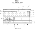
- FIG. 1 is a cross-sectional view illustrating an LCD according to the related art.
- the related art LCD 10 includes a liquid crystal panel having a first substrate 2 and a second substrate 4 attached to each other with a liquid crystal layer 50 therebetween, and a backlight 60.
- a thin film transistor Tr on the first substrate 2 includes a gate electrode 12, a gate insulating layer 13, an active layer 14, ohmic contact layers 15a and 15b, and source and drain electrodes 16 and 17, and is connected to a first electrode 19 in a pixel region 19 through a contact hole formed in an inter-layered insulating film 18.
- a black matrix 32 is below the second substrate 4, and has a lattice shape to surround the pixel region P such that the black matrix 32 shields a non-display element such as the thin film transistor Tr and exposes the first electrode 19.
- a color filter 34 is arranged in the lattice-shaped black matrix 32 corresponding to the pixel region P, and a second electrode is arranged to cover the black matrix 32 and the color filter 34.
- Polarizing plates 20 and 30 each selectively transmitting a predetermined polarized light are attached below the first substrate 2 and on the second substrate 4, respectively.
- a first alignment layer 31a having a surface rubbed in a predetermined direction is between the liquid crystal layer 50 and the first electrode 19
- a second alignment layer 31b having a surface rubbed in a predetermined direction is between the liquid crystal layer 50 and the second electrode 36, and thus initial arrangement state and alignment direction of liquid crystal molecules are uniform.
- a seal pattern 70 is arranged along edge portions of the first and second substrates 2 and 4.
- the backlight 60 as a light source is arranged below the liquid crystal panel to supply light to the liquid crystal panel.
- nematic liquid crystal As the liquid crystal layer for the LCD 10, a nematic liquid crystal, a smectic liquid crystal, a cholesteric liquid crystal or the like is used, and the nematic liquid crystal is mostly used.
- a gap between the two substrates 2 and 4 needs to be maintained after attaching the substrates 2 and 4and injecting the liquid crystal between the substrates 2 and 4, and if a gap between the two substrates changes by an external pressure or impact, display quality may be degraded.
- the present invention is directed to an LCD that substantially obviates one or more of the problems due to limitations and disadvantages of the related art.
- An object of the present invention is to provide an LCD that can reduce a driving voltage to drive a nano capsule liquid crystal layer.
- a nano capsule liquid crystal layer includes a buffer layer ; a plurality of nano capsules disposed in the buffer layer, an inside of each of the nano capsules including: liquid crystal molecules, and additives each having a center molecule and at least two first peripheral molecules connected to the center molecule and spaced apart from each other, and that are mixed with the liquid crystal molecules, wherein the first peripheral molecules have the same phase as the liquid crystal molecules.
- the center molecule has a linear structure, plate structure, or three-dimensional structure.
- the first peripheral molecules are located in different directions, and the additives have a three-dimensional structure.
- each of the additives further includes a second peripheral molecule that is connected to the center molecule and has a phase different from the first peripheral molecules.
- the center molecule has a dendrimer structure, and the first and second peripheral molecules are connected with ends of the dendrimer.
- each of the additives further includes a connection molecule connecting the center molecule with each of the first and second peripheral molecules.
- each of the additives further includes a connection molecule connecting the center molecule with each of the first peripheral molecules.
- a wt% of the additives is 0.01 to 25 to the liquid crystal molecules.
- a liquid crystal display device may include a substrate; first and second electrodes spaced apart from each other on the substrate; a nano capsule liquid crystal layer according to one or more embodiments described herein that is on the first and second electrodes; and first and second polarizing plates having first and second polarization axes, respectively, perpendicular to each other, the first polarizing plate below the substrate, the second polarizing plate on the nano capsule liquid crystal layer.
- a liquid crystal display device in another aspect, includes a substrate, first and second electrodes spaced apart from each other on the substrate, a nano capsule liquid crystal layer that is on the first and second electrodes and includes liquid crystal molecules filling an inside of a nano capsule, additives that each includes a center molecule and at least two first peripheral molecules connected with the center line and spaced apart from each other and that are mixed with the liquid crystal molecules in the nano capsule, and a buffer layer in which the nano capsules are spread, and first and second polarizing plates having first and second polarization axes, respectively, perpendicular to each other, the first polarizing plate below the substrate, the second polarizing plate on the nano capsule liquid crystal layer, wherein the first peripheral molecule has the same phase as the liquid crystal molecule.
- FIG. 2 is a cross-sectional view illustrating an LCD according to an embodiment of the present invention.
- the LCD 100 of the embodiment includes a substrate 101, first and second electrodes 120 and 130 on the substrate 101, a nano capsule liquid crystal layer 140 on the first and second electrodes 120 and 130, and first and second polarizing plates 159 and 160 that are below the substrate 101 and on the nano capsule liquid crystal layer 140, respectively.
- the nano capsule liquid crystal layer 140 is formed with nano capsules 142 that are dispersed in a buffer layer 143, and the nano capsule 142 has a size less than wavelengths of a visible light and is filled with liquid crystal molecules 141 randomly arranged.
- the nano capsule liquid crystal layer 140 may be formed in a film type over the first and second electrodes 120 and 130.
- the LCD 100 of this embodiment can be manufactured with one substrate 101, and thus the LCD of light weight and thin profile can be achieved, and production cost can be reduced.
- the nano capsule liquid crystal layer 140 does not have the problem of the related art that the gap between the related art two substrates goes awry or changes by an external pressure or impact.
- the nano capsule liquid crystal layer 140 can be effectively applied to a flexible LCD.
- the nano capsule liquid crystal layer 140 has an optical isotropy when an electric filed is not applied.
- the nano capsule liquid crystal layer 140 has an optical property that when an electric field is applied, the liquid crystal molecules 141 in the nano capsule 142 are aligned in a direction of the electric field and birefringence of a light incident on the nano capsule liquid crystal layer 140 is produced.
- the nano capsule liquid crystal layer 140 can form an optical axis according to an applied electric field, and by controlling an optical property using this, a light can be transmitted.
- the first polarizing plate 159 produces a polarization of a light to be incident on the nano capsule liquid crystal layer 140 from the backlight 170.
- the second polarizing plate 160 blocks a light that is incident on the nano capsule liquid crystal layer 140 and then passes through the nano capsule liquid crystal layer 140 without polarization by a birefringence effect of the nano capsule liquid crystal layer 140.
- a polarization axis of the first polarizing plate 159 and a polarization axis of the second polarizing plate 160 are perpendicular to each other. For example, if the polarization axis of the first polarizing plate 159 has a 0 or 90 degrees angle, the polarization axis of the second polarization plate 160 has a 90 or 0 degrees angle.
- the nano capsule liquid crystal layer 140 passes through a light entering it through the first polarizing plate 159, and thus the LCD 100 displays a black state.
- a light entering the first polarizing plate 159 from the backlight 170 is selectively transmitted at a specific angle while passing through the first polarization plate 159, then the light entering the nano capsule liquid crystal layer 140 is transmitted through the nano capsule liquid crystal layer 140 with a scattering phenomenon hardly happening and then reaches the second polarizing plate 160.
- a light passing through the first polarization plate 159 having the polarization axis of, for example, 0 degrees angle enters the second polarization plate 160 having the polarization axis of, for example, 90 degrees angle, thus this light is blocked by the second polarizing plate 160 perpendicular in polarizing axis to the first polarizing plate 159, and thus the LCD 100 displays the black state.
- the LCD 100 of this embodiment can display the black state using the optical property of the nano capsule liquid crystal layer 140 and thus does not require an alignment of a liquid crystal additionally.
- the LCD 100 of this embodiment can eliminate processes of printing and rubbing an alignment layer that the related art LCD necessarily requires.
- the nano capsule liquid crystal layer 140 rotates a polarization axis of a light entering the nano capsule liquid crystal layer 140 through the first polarization plate 159 by 90 degrees angle, and thus the LCD 100 displays a white state.
- a light entering the nano capsule liquid crystal layer 140 through the first polarizing plate 159 changes in polarization by the birefringence effect of the nano capsule liquid crystal layer 140.
- a retardation, ⁇ n*d, of the nano capsule liquid crystal layer 140 meets a ⁇ /2 condition of a light incident thereon, a polarization axis of the incident light is rotated by 90 degrees angle, thus this light is not absorbed by the second polarizing plate 160 perpendicular in polarization axis to the first polarizing plate 159 and passes through the second polarizing plate 160, and thus the LCD 100 displays the white state.
- the nano capsule 142 As a size of the nano capsule 142 increases, a light scattering may happen between the nano capsules 142 or liquid crystal molecules 141 and thus a full black state is not displayed in an off state of no electric field being applied. Accordingly, the nano capsule 142 preferably has a size less than wavelengths of a visible light.
- liquid crystal molecules 141 are located in the nano capsule 142, an attraction force between the liquid crystal molecules 141 and an attraction force between the liquid crystal molecule 141 and the nano capsule 142 are strong, and thus a driving voltage to drive the nano capsule liquid crystal layer 140 is much greater than that of the related art LCD (10 of FIG. 1 ).
- an attraction force between the liquid crystal molecules 141 and an attraction force between the liquid crystal molecule 141 and the nano capsule 142 can be reduced.
- a physical property of the liquid crystal including the liquid crystal molecules 141 may change, and a driving available temperature (Tni) of the nano capsule liquid crystal layer 140 may be lowered.
- a reliability and a driving property of the LCD 100 may be degraded, and particularly, a display quality at a high temperature may be degraded.
- FIG. 3 is a view illustrating a nano capsule according to an embodiment of the present invention
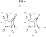
- FIG. 4 is a view illustrating additives in the nano capsule of FIG. 3
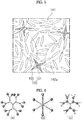
- FIG. 5 is a view illustrating a portion in the nano capsule of FIG. 3 .
- the nano capsule 142 includes liquid crystal molecules 141 filling the inside of the nano capsule 142, and additives 150 mixed with the liquid crystal molecules 141.
- the nano capsule 142 has a nano size less than wavelengths of a visible light.
- the nano capsule 142 may be made of one selected from a transparent silicon material group consisting a silicon nitride (SiNx) or silicon oxide (SiO 2 ), or one selected from a transparent polymer group consisting of polystyrene, poly ethylene poly urethane, poly chloride vinyl, poly methyl methane acrylate, poly carbonate epoxy resin, and poly vinyl acrylate.
- the liquid crystal molecules 141 are arranged randomly in the nano capsule 142, and may be made of a nematic liquid crystal, smectic liquid crystal, or cholesteric liquid crystal.
- the additive 150 includes a center molecule 151 and at least two first peripheral molecules 155 that each are connected to the center molecule 151 and are spaced apart from each other.
- the first peripheral molecule 155 has the same phase and property as the liquid crystal molecule 141.
- the first peripheral molecule 155 is easily mixed with the liquid crystal molecule 141, and a physical property of the liquid crystal including the first peripheral molecule 155 and its adjacent liquid crystal molecule 141 does not change.
- the center molecule 151 functions to support the first peripheral molecule 155. Since the center molecule 151 does not contact the liquid crystal molecule 141 by the first peripheral molecule 155, it is uniformly mixed with the liquid crystal molecule 141 and behaves like the same material.
- center molecule 151 may have a linear structure, plate structure, or three-dimensional structure.
- the first peripheral molecules 155 connected to the center molecule 151 are located in different directions so that the additive 150 can have a three-dimensional structure.
- the peripheral molecules 155 of the additive 150 breaks random arrangement of the liquid crystal molecules 141 around the first peripheral molecules 155 and makes the liquid crystal molecules 141 around the first peripheral molecules 155 arranged regularly in an arrangement direction of the first peripheral molecules 155 such that the liquid crystal molecules 141 forms a shape of a virtual sphere 142a in the nano capsule 142.
- the neighboring virtual spheres 142a overlap each other and spare the liquid crystal molecules 141 included therein.
- the virtual sphere 142a formed by the first peripheral molecules 155 can show an effect like forming the nano capsule 142 in a small size.
- the nano capsule 142 is divided into virtual spheres 142a having a size less than that of the nano capsule 142, a light scattering between the nano capsules 142 or between the liquid crystal molecules 141 can be prevented, and a full black can be displayed in an off state of no electric field being not applied.
- the first peripheral molecule 155 has the same phase and property as the liquid crystal molecule 141, the physical property of the liquid crystal molecule 141 can be prevented from changing, and a phenomenon of the driving available temperature (Tni) of the nano capsule liquid crystal layer 140 being lowered can be prevented.
- Table 1 shows a driving available temperature (Tni) and a refractive index variant ( ⁇ n) of the nano capsule liquid crystal layer 140 according to wt% of the additives 150 to the liquid crystal molecules 141.
- Tni driving available temperature
- ⁇ n refractive index variant
- the driving available temperature (Tni) and the refractive index variant ( ⁇ n) does not change much.
- wt% of the additives 150 is preferably 0.01 to 25 wt% to the liquid crystal molecules 141.
- the size of the additive 150 is 2nm to 100nm, which is greater than the liquid crystal molecule 141 and is less than the nano capsule 142.
- the additive 150 may include the center molecule 151 and first peripheral molecules 155 connected to the center molecule 151.
- the additive 150 may include the center molecule 151 and first and second peripheral molecules 155 and 157 connected to the center molecule 151.
- the second peripheral molecule 157 has a property different from the liquid crystal molecule 141, and the first peripheral molecule 155 may be made of an organic material and the second peripheral molecule 157 may be made of an inorganic material.
- the additive 150 includes the center molecule 151 and the first and second peripheral molecules 155 and 157, since the second peripheral molecules 157 has a phase and a property different from the liquid crystal molecule 141, and the fluidity of the liquid crystal molecules 141 can increase.
- the liquid crystal molecule 141 can be made fluid by a repulsive force between the second peripheral molecule 157 and the liquid crystal molecule 141.
- the liquid crystal molecules 141 When the fluidity of the liquid crystal molecules 141 increase, the liquid crystal molecules 141 can be rotated rapidly in an on state of an electric field being applied, and a response speed can be improved.
- the additive 150 may further include connection molecules 153 connecting the center molecule 151 with the first peripheral molecules 155 or the first and second peripheral molecules.
- a dendrimer structure is formed by the combination of the center molecule 151 and the connection molecules 153, and the center molecule 151 is connected indirectly with the peripheral molecules through the connection molecules 153.
- the center molecule 151 may has a dendrimer structure, and in this case, ends of the dendrimer of the center molecule 151 are combined with the respective peripheral molecules and the center molecule 151 is connected directly with the peripheral molecules.
- the first peripheral molecule 155 can make its adjacent liquid crystal molecule 141 arranged regularly in a direction to the first peripheral molecule 155.
- FIG. 6 is a view illustrating examples of a molecule having a dendrimer structure.
- a molecule of a dendrimer structure has a form (a), (b), or (c) in which a unit structure of a tree branch shape are spread from a center.
- FIGs. 7(a) and 7(b) are SSQMA and SSQOG, respectively, as examples of a center molecule.
- each of the SSQMA and SSQOG has a three-dimensional structure of a cube, and includes a dendrimer extending from corners of the cube.
- the first peripheral molecules 155 or the first and second peripheral molecules 155 and 157 are combined with the respective ends of the dendrimer of each of the SSQMA and SSQOG, and thus the additive 150 of the embodiment is finally formed.
- FIG. 8 is a graph illustrating an effect according to an embodiment of the present invention.
Landscapes
- Physics & Mathematics (AREA)
- Nonlinear Science (AREA)
- Chemical & Material Sciences (AREA)
- Crystallography & Structural Chemistry (AREA)
- General Physics & Mathematics (AREA)
- Mathematical Physics (AREA)
- Optics & Photonics (AREA)
- Dispersion Chemistry (AREA)
- Geometry (AREA)
- Spectroscopy & Molecular Physics (AREA)
- Organic Chemistry (AREA)
- Materials Engineering (AREA)
- Engineering & Computer Science (AREA)
- Liquid Crystal (AREA)
Abstract
Description
- The present application claims the priority benefit of Korean Patent Application No.
10-2015-0169521 - The present invention relates to a liquid crystal display device (LCD). In particular, the present invention relates to an LCD including a nano capsule liquid crystal layer.
- With the advancement of information society, the display field of displaying electric information signals has been rapidly advanced. Accordingly, as flat display devices having advantages of thin profile, light weight and low power consumption, a liquid crystal display device (LCD), a plasma display panel device (PDP), an electroluminescent display device (ELD), a field emission display device (FED) and the like have been introduced and have rapidly replaced a conventional cathode ray tube (CRT).
- Among the flat display devices, LCDs are most widely used in the fields of a laptop, monitor, television (TV) because they are excellent in displaying moving images and a high contrast ratio.
-
FIG. 1 is a cross-sectional view illustrating an LCD according to the related art. - Referring to
FIG. 1 , therelated art LCD 10 includes a liquid crystal panel having afirst substrate 2 and asecond substrate 4 attached to each other with aliquid crystal layer 50 therebetween, and abacklight 60. - In detail, a thin film transistor Tr on the
first substrate 2 includes agate electrode 12, agate insulating layer 13, anactive layer 14,ohmic contact layers drain electrodes first electrode 19 in apixel region 19 through a contact hole formed in an inter-layeredinsulating film 18. - Further, a
black matrix 32 is below thesecond substrate 4, and has a lattice shape to surround the pixel region P such that theblack matrix 32 shields a non-display element such as the thin film transistor Tr and exposes thefirst electrode 19. - Further, a
color filter 34 is arranged in the lattice-shapedblack matrix 32 corresponding to the pixel region P, and a second electrode is arranged to cover theblack matrix 32 and thecolor filter 34. - Polarizing
plates first substrate 2 and on thesecond substrate 4, respectively. - Further, a
first alignment layer 31a having a surface rubbed in a predetermined direction is between theliquid crystal layer 50 and thefirst electrode 19, and asecond alignment layer 31b having a surface rubbed in a predetermined direction is between theliquid crystal layer 50 and thesecond electrode 36, and thus initial arrangement state and alignment direction of liquid crystal molecules are uniform. - Further, to prevent a leakage of the
liquid crystal layer 50, aseal pattern 70 is arranged along edge portions of the first andsecond substrates - Since the
LCD 10 is not self-luminescent, thebacklight 60 as a light source is arranged below the liquid crystal panel to supply light to the liquid crystal panel. - As the liquid crystal layer for the
LCD 10, a nematic liquid crystal, a smectic liquid crystal, a cholesteric liquid crystal or the like is used, and the nematic liquid crystal is mostly used. - However, in the
related art LCD 10, there is an disadvantage that an alignment process when attaching the twosubstrates substrates - Further, processes of printing and rubbing the
alignment layers - Further, a gap between the two
substrates substrates 2 and 4and injecting the liquid crystal between thesubstrates - Accordingly, the present invention is directed to an LCD that substantially obviates one or more of the problems due to limitations and disadvantages of the related art.
- An object of the present invention is to provide an LCD that can reduce a driving voltage to drive a nano capsule liquid crystal layer.
- Additional features and advantages of the disclosure will be set forth in the description which follows, and in part will be apparent from the description, or may be learned by practice of the disclosure. The advantages of the disclosure will be realized and attained by the structure particularly pointed out in the written description and claims as well as the appended drawings.
- To achieve these and other advantages, and in accordance with the purpose of the present invention, as embodied and broadly described herein, a nano capsule liquid crystal layer includes a buffer layer ; a plurality of nano capsules disposed in the buffer layer, an inside of each of the nano capsules including: liquid crystal molecules, and additives each having a center molecule and at least two first peripheral molecules connected to the center molecule and spaced apart from each other, and that are mixed with the liquid crystal molecules, wherein the first peripheral molecules have the same phase as the liquid crystal molecules.
- In one or more embodiments, the center molecule has a linear structure, plate structure, or three-dimensional structure.
- In one or more embodiments, the first peripheral molecules are located in different directions, and the additives have a three-dimensional structure.
- In one or more embodiments, each of the additives further includes a second peripheral molecule that is connected to the center molecule and has a phase different from the first peripheral molecules.
- In one or more embodiments, the center molecule has a dendrimer structure, and the first and second peripheral molecules are connected with ends of the dendrimer.
- In one or more embodiments, each of the additives further includes a connection molecule connecting the center molecule with each of the first and second peripheral molecules.
- In one or more embodiments, each of the additives further includes a connection molecule connecting the center molecule with each of the first peripheral molecules.
- In one or more embodiments, a wt% of the additives is 0.01 to 25 to the liquid crystal molecules.
- A liquid crystal display device according to various embodiments may include a substrate; first and second electrodes spaced apart from each other on the substrate; a nano capsule liquid crystal layer according to one or more embodiments described herein that is on the first and second electrodes; and first and second polarizing plates having first and second polarization axes, respectively, perpendicular to each other, the first polarizing plate below the substrate, the second polarizing plate on the nano capsule liquid crystal layer.
- In another aspect, a liquid crystal display device includes a substrate, first and second electrodes spaced apart from each other on the substrate, a nano capsule liquid crystal layer that is on the first and second electrodes and includes liquid crystal molecules filling an inside of a nano capsule, additives that each includes a center molecule and at least two first peripheral molecules connected with the center line and spaced apart from each other and that are mixed with the liquid crystal molecules in the nano capsule, and a buffer layer in which the nano capsules are spread, and first and second polarizing plates having first and second polarization axes, respectively, perpendicular to each other, the first polarizing plate below the substrate, the second polarizing plate on the nano capsule liquid crystal layer, wherein the first peripheral molecule has the same phase as the liquid crystal molecule.
- It is to be understood that both the foregoing general description and the following detailed description are exemplary and explanatory and are intended to provide further explanation of the invention as claimed.
- The accompanying drawings, which are included to provide a further understanding of the disclosure and are incorporated in and constitute a part of this specification, illustrate embodiments of the disclosure and together with the description serve to explain the principles of the disclosure. In the drawings:
-
FIG. 1 is a cross-sectional view illustrating an LCD according to the related art; -
FIG. 2 is a cross-sectional view illustrating an LCD according to an embodiment of the present invention; -
FIG. 3 is a view illustrating a nano capsule according to an embodiment of the present invention; -
FIG. 4 is a view illustrating additives in the nano capsule ofFIG. 3 ; -
FIG. 5 is a view illustrating a portion in the nano capsule ofFIG. 3 ; -
FIG. 6 is a view illustrating examples of a molecule having a dendrimer structure; -
FIG. 7 is a view illustrating examples of a center molecule of an additive; and -
FIG. 8 is a graph illustrating an effect according to an embodiment of the present invention. - Reference will now be made in detail to embodiments, examples of which are illustrated in the accompanying drawings. The same or like reference numbers may be used throughout the drawings to refer to the same or like parts.
-
FIG. 2 is a cross-sectional view illustrating an LCD according to an embodiment of the present invention. - Referring to
FIG. 2 , theLCD 100 of the embodiment includes asubstrate 101, first andsecond electrodes substrate 101, a nano capsuleliquid crystal layer 140 on the first andsecond electrodes plates substrate 101 and on the nano capsuleliquid crystal layer 140, respectively. - The nano capsule
liquid crystal layer 140 is formed withnano capsules 142 that are dispersed in abuffer layer 143, and thenano capsule 142 has a size less than wavelengths of a visible light and is filled withliquid crystal molecules 141 randomly arranged. - The nano capsule
liquid crystal layer 140 may be formed in a film type over the first andsecond electrodes - Accordingly, unlike the related art LCD using two substrates, the
LCD 100 of this embodiment can be manufactured with onesubstrate 101, and thus the LCD of light weight and thin profile can be achieved, and production cost can be reduced. - Further, the nano capsule
liquid crystal layer 140 does not have the problem of the related art that the gap between the related art two substrates goes awry or changes by an external pressure or impact. Thus, when forming thesubstrate 101 using a flexible material such as a plastic, the nano capsuleliquid crystal layer 140 can be effectively applied to a flexible LCD. - Further, the nano capsule
liquid crystal layer 140 has an optical isotropy when an electric filed is not applied. However, the nano capsuleliquid crystal layer 140 has an optical property that when an electric field is applied, theliquid crystal molecules 141 in thenano capsule 142 are aligned in a direction of the electric field and birefringence of a light incident on the nano capsuleliquid crystal layer 140 is produced. - Accordingly, the nano capsule
liquid crystal layer 140 can form an optical axis according to an applied electric field, and by controlling an optical property using this, a light can be transmitted. - Further, the first polarizing
plate 159 produces a polarization of a light to be incident on the nano capsuleliquid crystal layer 140 from thebacklight 170. The second polarizingplate 160 blocks a light that is incident on the nano capsuleliquid crystal layer 140 and then passes through the nano capsuleliquid crystal layer 140 without polarization by a birefringence effect of the nano capsuleliquid crystal layer 140. - A polarization axis of the first polarizing
plate 159 and a polarization axis of the second polarizingplate 160 are perpendicular to each other. For example, if the polarization axis of the first polarizingplate 159 has a 0 or 90 degrees angle, the polarization axis of thesecond polarization plate 160 has a 90 or 0 degrees angle. - A principle of operating the
LCD 100 including the nano capsuleliquid crystal layer 140 is explained below. - First, when an electric field is not induced between the first and
second electrodes liquid crystal layer 140 passes through a light entering it through the firstpolarizing plate 159, and thus theLCD 100 displays a black state. - In other words, in the off state with no electric field being applied, a light entering the first
polarizing plate 159 from thebacklight 170 is selectively transmitted at a specific angle while passing through thefirst polarization plate 159, then the light entering the nano capsuleliquid crystal layer 140 is transmitted through the nano capsuleliquid crystal layer 140 with a scattering phenomenon hardly happening and then reaches the secondpolarizing plate 160. - Finally, a light passing through the
first polarization plate 159 having the polarization axis of, for example, 0 degrees angle enters thesecond polarization plate 160 having the polarization axis of, for example, 90 degrees angle, thus this light is blocked by the secondpolarizing plate 160 perpendicular in polarizing axis to the firstpolarizing plate 159, and thus theLCD 100 displays the black state. - As described above, unlike the related art LCD requiring that a pair of alignment layers are arranged on a pair of substrates opposing to each other, respectively, and a liquid crystal is injected between the substrates and is align to have predetermined pitch and direction, the
LCD 100 of this embodiment can display the black state using the optical property of the nano capsuleliquid crystal layer 140 and thus does not require an alignment of a liquid crystal additionally. - Accordingly, the
LCD 100 of this embodiment can eliminate processes of printing and rubbing an alignment layer that the related art LCD necessarily requires. - When an electric field is induced between the first and
second electrodes liquid crystal layer 140 rotates a polarization axis of a light entering the nano capsuleliquid crystal layer 140 through thefirst polarization plate 159 by 90 degrees angle, and thus theLCD 100 displays a white state. - In detail, in the on state with the electric field being induced, since the
liquid crystal molecules 141 in thenano capsule 142 are arranged in parallel with a direction of the electric field, a birefringence effect by the alignment of theliquid crystal molecules 141 is produced. - In this case, a light entering the nano capsule
liquid crystal layer 140 through the firstpolarizing plate 159 changes in polarization by the birefringence effect of the nano capsuleliquid crystal layer 140. When a retardation, Δn*d, of the nano capsuleliquid crystal layer 140 meets a λ/2 condition of a light incident thereon, a polarization axis of the incident light is rotated by 90 degrees angle, thus this light is not absorbed by the secondpolarizing plate 160 perpendicular in polarization axis to the firstpolarizing plate 159 and passes through the secondpolarizing plate 160, and thus theLCD 100 displays the white state. - As a size of the
nano capsule 142 increases, a light scattering may happen between thenano capsules 142 orliquid crystal molecules 141 and thus a full black state is not displayed in an off state of no electric field being applied. Accordingly, thenano capsule 142 preferably has a size less than wavelengths of a visible light. - Further, since the
liquid crystal molecules 141 are located in thenano capsule 142, an attraction force between theliquid crystal molecules 141 and an attraction force between theliquid crystal molecule 141 and thenano capsule 142 are strong, and thus a driving voltage to drive the nano capsuleliquid crystal layer 140 is much greater than that of the related art LCD (10 ofFIG. 1 ). - To reduce the driving voltage, by adding impurities into the
nano capsule 142, an attraction force between theliquid crystal molecules 141 and an attraction force between theliquid crystal molecule 141 and thenano capsule 142 can be reduced. - However, because of the added impurities, a physical property of the liquid crystal including the
liquid crystal molecules 141 may change, and a driving available temperature (Tni) of the nano capsuleliquid crystal layer 140 may be lowered. - Accordingly, a reliability and a driving property of the
LCD 100 may be degraded, and particularly, a display quality at a high temperature may be degraded. -
FIG. 3 is a view illustrating a nano capsule according to an embodiment of the present invention,FIG. 4 is a view illustrating additives in the nano capsule ofFIG. 3 , andFIG. 5 is a view illustrating a portion in the nano capsule ofFIG. 3 . - Referring to
FIG. 3 , thenano capsule 142 includesliquid crystal molecules 141 filling the inside of thenano capsule 142, andadditives 150 mixed with theliquid crystal molecules 141. - In detail, the
nano capsule 142 has a nano size less than wavelengths of a visible light. Thenano capsule 142 may be made of one selected from a transparent silicon material group consisting a silicon nitride (SiNx) or silicon oxide (SiO2), or one selected from a transparent polymer group consisting of polystyrene, poly ethylene poly urethane, poly chloride vinyl, poly methyl methane acrylate, poly carbonate epoxy resin, and poly vinyl acrylate. - The
liquid crystal molecules 141 are arranged randomly in thenano capsule 142, and may be made of a nematic liquid crystal, smectic liquid crystal, or cholesteric liquid crystal. - Referring to
FIG. 4 , the additive 150 includes acenter molecule 151 and at least two firstperipheral molecules 155 that each are connected to thecenter molecule 151 and are spaced apart from each other. - The first
peripheral molecule 155 has the same phase and property as theliquid crystal molecule 141. - Accordingly, the first
peripheral molecule 155 is easily mixed with theliquid crystal molecule 141, and a physical property of the liquid crystal including the firstperipheral molecule 155 and its adjacentliquid crystal molecule 141 does not change. - The
center molecule 151 functions to support the firstperipheral molecule 155. Since thecenter molecule 151 does not contact theliquid crystal molecule 141 by the firstperipheral molecule 155, it is uniformly mixed with theliquid crystal molecule 141 and behaves like the same material. - Further, the
center molecule 151 may have a linear structure, plate structure, or three-dimensional structure. The firstperipheral molecules 155 connected to thecenter molecule 151 are located in different directions so that the additive 150 can have a three-dimensional structure. - Accordingly, referring to
FIG. 5 , theperipheral molecules 155 of the additive 150 breaks random arrangement of theliquid crystal molecules 141 around the firstperipheral molecules 155 and makes theliquid crystal molecules 141 around the firstperipheral molecules 155 arranged regularly in an arrangement direction of the firstperipheral molecules 155 such that theliquid crystal molecules 141 forms a shape of avirtual sphere 142a in thenano capsule 142. - In this case, the neighboring
virtual spheres 142a overlap each other and spare theliquid crystal molecules 141 included therein. - The
virtual sphere 142a formed by the firstperipheral molecules 155 can show an effect like forming thenano capsule 142 in a small size. - In other words, since the
nano capsule 142 is divided intovirtual spheres 142a having a size less than that of thenano capsule 142, a light scattering between thenano capsules 142 or between theliquid crystal molecules 141 can be prevented, and a full black can be displayed in an off state of no electric field being not applied. - Further, by not reducing a size of the
nano capsule 142 and filling it with theliquid crystal molecules 141 but forming thevirtual spheres 142a in thenano capsule 142 having a predetermined size, an effect like size reduction is shown. Accordingly, an attraction force between theliquid crystal molecules 141 and an attraction force between thenano capsule 142 and theliquid crystal molecule 141 are not strong, and thus a driving voltage to drive the nano capsuleliquid crystal layer 140 does not rise. - Further, since the first
peripheral molecule 155 has the same phase and property as theliquid crystal molecule 141, the physical property of theliquid crystal molecule 141 can be prevented from changing, and a phenomenon of the driving available temperature (Tni) of the nano capsuleliquid crystal layer 140 being lowered can be prevented. - Table 1 shows a driving available temperature (Tni) and a refractive index variant (Δn) of the nano capsule
liquid crystal layer 140 according to wt% of theadditives 150 to theliquid crystal molecules 141.[Table 1] 0.0 wt% 0.1 wt% 1 wt% 1.25 wt% 1.5wt% Tni(°C) 89.9 89.9 89.9 89.4 88.7 Δn 0.2493 0.2492 0.2491 0.2471 0.2450 - Referring to Table 1, in a case of adding the
additives 150 with a certain amount (0.1 wt%, 1 wt%, 1.25wt%, and 2.5wt%) compared with a case of adding noadditives 150, the driving available temperature (Tni) and the refractive index variant (Δn) does not change much. - However, when the
additives 150 are contained greater than theliquid crystal molecules 141 in thenano capsule 142, a fluidity of theliquid crystal molecules 141 is reduced and a driving efficiency is reduced. Accordingly, wt% of theadditives 150 is preferably 0.01 to 25 wt% to theliquid crystal molecules 141. - The size of the additive 150 is 2nm to 100nm, which is greater than the
liquid crystal molecule 141 and is less than thenano capsule 142. - Referring to
FIG. 4(a) , the additive 150 may include thecenter molecule 151 and firstperipheral molecules 155 connected to thecenter molecule 151. Alternatively, referring toFIG. 4(b) , the additive 150 may include thecenter molecule 151 and first and secondperipheral molecules center molecule 151. - The second
peripheral molecule 157 has a property different from theliquid crystal molecule 141, and the firstperipheral molecule 155 may be made of an organic material and the secondperipheral molecule 157 may be made of an inorganic material. - Particularly, in the case that the additive 150 includes the
center molecule 151 and the first and secondperipheral molecules peripheral molecules 157 has a phase and a property different from theliquid crystal molecule 141, and the fluidity of theliquid crystal molecules 141 can increase. - In other words, since the second
peripheral molecules 157 are not easily mixed with theliquid crystal molecules 141, theliquid crystal molecule 141 can be made fluid by a repulsive force between the secondperipheral molecule 157 and theliquid crystal molecule 141. - When the fluidity of the
liquid crystal molecules 141 increase, theliquid crystal molecules 141 can be rotated rapidly in an on state of an electric field being applied, and a response speed can be improved. - Further, referring to
FIGs. 4(a) and 4(b) , the additive 150 may further includeconnection molecules 153 connecting thecenter molecule 151 with the firstperipheral molecules 155 or the first and second peripheral molecules. - In other words, a dendrimer structure is formed by the combination of the
center molecule 151 and theconnection molecules 153, and thecenter molecule 151 is connected indirectly with the peripheral molecules through theconnection molecules 153. - Alternatively, the
center molecule 151 may has a dendrimer structure, and in this case, ends of the dendrimer of thecenter molecule 151 are combined with the respective peripheral molecules and thecenter molecule 151 is connected directly with the peripheral molecules. - By adjusting a length of the
connection molecule 143 or the dendrimer, or adjusting a size of the firstperipheral molecule 155, the firstperipheral molecule 155 can make its adjacentliquid crystal molecule 141 arranged regularly in a direction to the firstperipheral molecule 155. -
FIG. 6 is a view illustrating examples of a molecule having a dendrimer structure. - Referring to
FIG. 6 , a molecule of a dendrimer structure has a form (a), (b), or (c) in which a unit structure of a tree branch shape are spread from a center. -
FIGs. 7(a) and 7(b) are SSQMA and SSQOG, respectively, as examples of a center molecule. - In detail, each of the SSQMA and SSQOG has a three-dimensional structure of a cube, and includes a dendrimer extending from corners of the cube.
- Accordingly, the first
peripheral molecules 155 or the first and secondperipheral molecules additive 150 of the embodiment is finally formed. -
FIG. 8 is a graph illustrating an effect according to an embodiment of the present invention. - Referring to
FIG. 8 , compared with a case (a) that a nano capsule is filled only with liquid crystal molecules, in a case (b) that additives are added, a driving property is improved, and a black level and a contrast ratio are improved, and an efficiency is improved.
Claims (9)
- A nano capsule liquid crystal layer (140), comprising:a buffer layer (143);a plurality of nano capsules (142) disposed in the buffer layer (143), an inside of each of the nano capsules (142) including:liquid crystal molecules (141), andadditives (150) each having a center molecule (151) and at least two first peripheral molecules (155) connected to the center molecule (151) and spaced apart from each other, and that are mixed with the liquid crystal molecules (141),wherein the first peripheral molecules (155) have the same phase as the liquid crystal molecules (141).
- The nano capsule liquid crystal layer (140) of claim 1, wherein the center molecule (151) has a linear structure, plate structure, or three-dimensional structure.
- The nano capsule liquid crystal layer (140) of claim 2, wherein the first peripheral molecules (155) are located in different directions, and the additives (150) have a three-dimensional structure.
- The nano capsule liquid crystal layer (140) of any one of claims 1 to 3, wherein each of the additives (150) further includes a second peripheral molecule (157) that is connected to the center molecule (151) and has a phase different from the first peripheral molecules (155).
- The nano capsule liquid crystal layer (140) of claim 4, wherein the center molecule (151) has a dendrimer structure, and the first and second peripheral molecules (155, 157) are connected with ends of the dendrimer.
- The nano capsule liquid crystal layer (140) of claim 4 or 5, wherein each of the additives (150) further includes a connection molecule (153) connecting the center molecule (151) with each of the first and second peripheral molecules (155, 157).
- The nano capsule liquid crystal layer (140) of claim 1, wherein each of the additives (150) further includes a connection molecule (153) connecting the center molecule (151) with each of the first peripheral molecules (155).
- The nano capsule liquid crystal layer (140) of claim 1, wherein a wt% of the additives (150), is 0.01 to 25 to the liquid crystal molecules (141).
- A liquid crystal display device (100), comprising:a substrate (101);first and second electrodes (120, 130) spaced apart from each other on the substrate (101);a nano capsule liquid crystal layer (140) according to any one of claims 1 to 8 that is on the first and second electrodes (120, 130); andfirst and second polarizing plates (159, 160) having first and second polarization axes, respectively, perpendicular to each other, the first polarizing plate (159) below the substrate (101), the second polarizing plate (160) on the nano capsule liquid crystal layer (140).
Applications Claiming Priority (1)
| Application Number | Priority Date | Filing Date | Title |
|---|---|---|---|
| KR1020150169521A KR102227240B1 (en) | 2015-11-30 | 2015-11-30 | Nano capsule liquid crystal and liquid crystal display device having the same |
Publications (2)
| Publication Number | Publication Date |
|---|---|
| EP3173863A1 true EP3173863A1 (en) | 2017-05-31 |
| EP3173863B1 EP3173863B1 (en) | 2020-06-10 |
Family
ID=57421754
Family Applications (1)
| Application Number | Title | Priority Date | Filing Date |
|---|---|---|---|
| EP16201078.9A Active EP3173863B1 (en) | 2015-11-30 | 2016-11-29 | Nano capsule liquid crystal layer and liquid crystal display device including the same |
Country Status (5)
| Country | Link |
|---|---|
| US (1) | US10018867B2 (en) |
| EP (1) | EP3173863B1 (en) |
| KR (1) | KR102227240B1 (en) |
| CN (1) | CN106908981B (en) |
| TW (1) | TWI634368B (en) |
Families Citing this family (2)
| Publication number | Priority date | Publication date | Assignee | Title |
|---|---|---|---|---|
| KR102496683B1 (en) | 2017-10-11 | 2023-02-07 | 삼성디스플레이 주식회사 | Display panel and display device comprising the display panel |
| US10845600B2 (en) | 2018-04-24 | 2020-11-24 | Samsung Electronics Co., Ltd. | Controllable modifiable shader layer for head mountable display |
Citations (3)
| Publication number | Priority date | Publication date | Assignee | Title |
|---|---|---|---|---|
| US20020001052A1 (en) * | 2000-04-05 | 2002-01-03 | Kornfield Julia A. | Polymers for control of orientation and stability of liquid crystals |
| US20120162596A1 (en) * | 2010-12-22 | 2012-06-28 | Photon Dynamics, Inc. | Encapsulated Polymer Network Liquid Crystal Material, Device and Applications |
| US20150109547A1 (en) * | 2013-10-23 | 2015-04-23 | Lg Display Co., Ltd. | Liquid crystal display including nanocapsule layer |
Family Cites Families (12)
| Publication number | Priority date | Publication date | Assignee | Title |
|---|---|---|---|---|
| US6203723B1 (en) * | 1998-03-12 | 2001-03-20 | Ying Yen Hsu | Microencapsulated liquid crystal having multidomains induced by the polymer network and method |
| US20030214690A1 (en) * | 2001-11-26 | 2003-11-20 | Escuti Michael J. | Holographic polymer photonic crystal |
| WO2005059637A1 (en) * | 2003-12-18 | 2005-06-30 | Sharp Kabushiki Kaisha | Display device |
| JP4142019B2 (en) | 2004-01-20 | 2008-08-27 | シャープ株式会社 | Display element and display device |
| US7817333B2 (en) | 2007-02-06 | 2010-10-19 | Photon Dynamics, Inc. | Modulator with improved sensitivity and life time |
| KR20120046532A (en) | 2010-11-02 | 2012-05-10 | 한국생명공학연구원 | Anti-biofouling ssq/peg network and method for preparing the same |
| US8988642B2 (en) * | 2010-11-09 | 2015-03-24 | Samsung Display Co., Ltd. | Liquid crystal display devices and methods of manufacturing liquid crystal display devices |
| US9006345B2 (en) * | 2011-03-25 | 2015-04-14 | The Trustees Of Columbia University In The City Of New York | Heterotrifunctional molecules and methods for the synthesis of dendrimeric materials |
| CN102929045B (en) * | 2012-10-08 | 2016-03-16 | 京东方科技集团股份有限公司 | High polymer dispersed liquid crystal panel and preparation method thereof, liquid crystal indicator |
| EP2933677B1 (en) * | 2012-12-14 | 2019-02-13 | LG Chem, Ltd. | Liquid crystal element |
| US9366920B2 (en) * | 2013-01-02 | 2016-06-14 | Lg Display Co., Ltd. | Liquid crystal display device and fabricating method thereof |
| KR102016958B1 (en) | 2013-01-02 | 2019-09-02 | 엘지디스플레이 주식회사 | Liquid crystal display and method for fabricating the same |
-
2015
- 2015-11-30 KR KR1020150169521A patent/KR102227240B1/en active Active
-
2016
- 2016-11-25 TW TW105138935A patent/TWI634368B/en not_active IP Right Cessation
- 2016-11-28 US US15/361,656 patent/US10018867B2/en active Active
- 2016-11-29 EP EP16201078.9A patent/EP3173863B1/en active Active
- 2016-11-30 CN CN201611080290.0A patent/CN106908981B/en active Active
Patent Citations (3)
| Publication number | Priority date | Publication date | Assignee | Title |
|---|---|---|---|---|
| US20020001052A1 (en) * | 2000-04-05 | 2002-01-03 | Kornfield Julia A. | Polymers for control of orientation and stability of liquid crystals |
| US20120162596A1 (en) * | 2010-12-22 | 2012-06-28 | Photon Dynamics, Inc. | Encapsulated Polymer Network Liquid Crystal Material, Device and Applications |
| US20150109547A1 (en) * | 2013-10-23 | 2015-04-23 | Lg Display Co., Ltd. | Liquid crystal display including nanocapsule layer |
Also Published As
| Publication number | Publication date |
|---|---|
| CN106908981A (en) | 2017-06-30 |
| TWI634368B (en) | 2018-09-01 |
| KR20170064171A (en) | 2017-06-09 |
| CN106908981B (en) | 2020-09-08 |
| EP3173863B1 (en) | 2020-06-10 |
| US20170192265A1 (en) | 2017-07-06 |
| KR102227240B1 (en) | 2021-03-12 |
| TW201728980A (en) | 2017-08-16 |
| US10018867B2 (en) | 2018-07-10 |
Similar Documents
| Publication | Publication Date | Title |
|---|---|---|
| US20160231609A1 (en) | Display device | |
| US20090219466A1 (en) | Electro-Optical Device and Display Device | |
| US20140211136A1 (en) | Liquid crystal display device | |
| KR102016958B1 (en) | Liquid crystal display and method for fabricating the same | |
| EP3173858B1 (en) | Liquid crystal display device | |
| EP3173863B1 (en) | Nano capsule liquid crystal layer and liquid crystal display device including the same | |
| KR101333614B1 (en) | Liquid crystal display device | |
| US9964794B2 (en) | Liquid crystal display device | |
| KR20140088471A (en) | Liquid crystal display and method for fabricating the same | |
| JP4381928B2 (en) | Liquid crystal display | |
| KR20120133927A (en) | Display device and method for manufacturing the same | |
| US7394512B2 (en) | Liquid crystal display device | |
| KR102362436B1 (en) | Liquid crystal display device | |
| US7382427B2 (en) | Liquid crystal display device | |
| US10197839B2 (en) | Liquid crystal display device and method of manufacturing the same | |
| KR102395571B1 (en) | Liquid crystal display device | |
| KR101429902B1 (en) | Liquid Crystal Display Device | |
| KR20160025677A (en) | Array substrate and liquid crystal display device including the same | |
| KR102162891B1 (en) | Liquid crystal composition and liquid crystal display device having the same |
Legal Events
| Date | Code | Title | Description |
|---|---|---|---|
| PUAI | Public reference made under article 153(3) epc to a published international application that has entered the european phase |
Free format text: ORIGINAL CODE: 0009012 |
|
| STAA | Information on the status of an ep patent application or granted ep patent |
Free format text: STATUS: REQUEST FOR EXAMINATION WAS MADE |
|
| 17P | Request for examination filed |
Effective date: 20161129 |
|
| AK | Designated contracting states |
Kind code of ref document: A1 Designated state(s): AL AT BE BG CH CY CZ DE DK EE ES FI FR GB GR HR HU IE IS IT LI LT LU LV MC MK MT NL NO PL PT RO RS SE SI SK SM TR |
|
| AX | Request for extension of the european patent |
Extension state: BA ME |
|
| R17P | Request for examination filed (corrected) |
Effective date: 20161129 |
|
| RBV | Designated contracting states (corrected) |
Designated state(s): AL AT BE BG CH CY CZ DE DK EE ES FI FR GB GR HR HU IE IS IT LI LT LU LV MC MK MT NL NO PL PT RO RS SE SI SK SM TR |
|
| GRAP | Despatch of communication of intention to grant a patent |
Free format text: ORIGINAL CODE: EPIDOSNIGR1 |
|
| STAA | Information on the status of an ep patent application or granted ep patent |
Free format text: STATUS: GRANT OF PATENT IS INTENDED |
|
| RIC1 | Information provided on ipc code assigned before grant |
Ipc: G02F 1/1334 20060101ALI20200217BHEP Ipc: G02F 1/1337 20060101ALI20200217BHEP Ipc: G02F 1/1343 20060101AFI20200217BHEP |
|
| INTG | Intention to grant announced |
Effective date: 20200320 |
|
| GRAS | Grant fee paid |
Free format text: ORIGINAL CODE: EPIDOSNIGR3 |
|
| GRAA | (expected) grant |
Free format text: ORIGINAL CODE: 0009210 |
|
| STAA | Information on the status of an ep patent application or granted ep patent |
Free format text: STATUS: THE PATENT HAS BEEN GRANTED |
|
| AK | Designated contracting states |
Kind code of ref document: B1 Designated state(s): AL AT BE BG CH CY CZ DE DK EE ES FI FR GB GR HR HU IE IS IT LI LT LU LV MC MK MT NL NO PL PT RO RS SE SI SK SM TR |
|
| REG | Reference to a national code |
Ref country code: GB Ref legal event code: FG4D |
|
| REG | Reference to a national code |
Ref country code: CH Ref legal event code: EP Ref country code: AT Ref legal event code: REF Ref document number: 1279652 Country of ref document: AT Kind code of ref document: T Effective date: 20200615 |
|
| REG | Reference to a national code |
Ref country code: DE Ref legal event code: R096 Ref document number: 602016037817 Country of ref document: DE |
|
| REG | Reference to a national code |
Ref country code: IE Ref legal event code: FG4D |
|
| REG | Reference to a national code |
Ref country code: LT Ref legal event code: MG4D |
|
| PG25 | Lapsed in a contracting state [announced via postgrant information from national office to epo] |
Ref country code: SE Free format text: LAPSE BECAUSE OF FAILURE TO SUBMIT A TRANSLATION OF THE DESCRIPTION OR TO PAY THE FEE WITHIN THE PRESCRIBED TIME-LIMIT Effective date: 20200610 Ref country code: LT Free format text: LAPSE BECAUSE OF FAILURE TO SUBMIT A TRANSLATION OF THE DESCRIPTION OR TO PAY THE FEE WITHIN THE PRESCRIBED TIME-LIMIT Effective date: 20200610 Ref country code: NO Free format text: LAPSE BECAUSE OF FAILURE TO SUBMIT A TRANSLATION OF THE DESCRIPTION OR TO PAY THE FEE WITHIN THE PRESCRIBED TIME-LIMIT Effective date: 20200910 Ref country code: GR Free format text: LAPSE BECAUSE OF FAILURE TO SUBMIT A TRANSLATION OF THE DESCRIPTION OR TO PAY THE FEE WITHIN THE PRESCRIBED TIME-LIMIT Effective date: 20200911 Ref country code: FI Free format text: LAPSE BECAUSE OF FAILURE TO SUBMIT A TRANSLATION OF THE DESCRIPTION OR TO PAY THE FEE WITHIN THE PRESCRIBED TIME-LIMIT Effective date: 20200610 |
|
| REG | Reference to a national code |
Ref country code: NL Ref legal event code: MP Effective date: 20200610 |
|
| PG25 | Lapsed in a contracting state [announced via postgrant information from national office to epo] |
Ref country code: HR Free format text: LAPSE BECAUSE OF FAILURE TO SUBMIT A TRANSLATION OF THE DESCRIPTION OR TO PAY THE FEE WITHIN THE PRESCRIBED TIME-LIMIT Effective date: 20200610 Ref country code: LV Free format text: LAPSE BECAUSE OF FAILURE TO SUBMIT A TRANSLATION OF THE DESCRIPTION OR TO PAY THE FEE WITHIN THE PRESCRIBED TIME-LIMIT Effective date: 20200610 Ref country code: BG Free format text: LAPSE BECAUSE OF FAILURE TO SUBMIT A TRANSLATION OF THE DESCRIPTION OR TO PAY THE FEE WITHIN THE PRESCRIBED TIME-LIMIT Effective date: 20200910 Ref country code: RS Free format text: LAPSE BECAUSE OF FAILURE TO SUBMIT A TRANSLATION OF THE DESCRIPTION OR TO PAY THE FEE WITHIN THE PRESCRIBED TIME-LIMIT Effective date: 20200610 |
|
| REG | Reference to a national code |
Ref country code: AT Ref legal event code: MK05 Ref document number: 1279652 Country of ref document: AT Kind code of ref document: T Effective date: 20200610 |
|
| PG25 | Lapsed in a contracting state [announced via postgrant information from national office to epo] |
Ref country code: NL Free format text: LAPSE BECAUSE OF FAILURE TO SUBMIT A TRANSLATION OF THE DESCRIPTION OR TO PAY THE FEE WITHIN THE PRESCRIBED TIME-LIMIT Effective date: 20200610 Ref country code: AL Free format text: LAPSE BECAUSE OF FAILURE TO SUBMIT A TRANSLATION OF THE DESCRIPTION OR TO PAY THE FEE WITHIN THE PRESCRIBED TIME-LIMIT Effective date: 20200610 |
|
| PG25 | Lapsed in a contracting state [announced via postgrant information from national office to epo] |
Ref country code: IT Free format text: LAPSE BECAUSE OF FAILURE TO SUBMIT A TRANSLATION OF THE DESCRIPTION OR TO PAY THE FEE WITHIN THE PRESCRIBED TIME-LIMIT Effective date: 20200610 Ref country code: RO Free format text: LAPSE BECAUSE OF FAILURE TO SUBMIT A TRANSLATION OF THE DESCRIPTION OR TO PAY THE FEE WITHIN THE PRESCRIBED TIME-LIMIT Effective date: 20200610 Ref country code: PT Free format text: LAPSE BECAUSE OF FAILURE TO SUBMIT A TRANSLATION OF THE DESCRIPTION OR TO PAY THE FEE WITHIN THE PRESCRIBED TIME-LIMIT Effective date: 20201012 Ref country code: AT Free format text: LAPSE BECAUSE OF FAILURE TO SUBMIT A TRANSLATION OF THE DESCRIPTION OR TO PAY THE FEE WITHIN THE PRESCRIBED TIME-LIMIT Effective date: 20200610 Ref country code: ES Free format text: LAPSE BECAUSE OF FAILURE TO SUBMIT A TRANSLATION OF THE DESCRIPTION OR TO PAY THE FEE WITHIN THE PRESCRIBED TIME-LIMIT Effective date: 20200610 Ref country code: SM Free format text: LAPSE BECAUSE OF FAILURE TO SUBMIT A TRANSLATION OF THE DESCRIPTION OR TO PAY THE FEE WITHIN THE PRESCRIBED TIME-LIMIT Effective date: 20200610 Ref country code: EE Free format text: LAPSE BECAUSE OF FAILURE TO SUBMIT A TRANSLATION OF THE DESCRIPTION OR TO PAY THE FEE WITHIN THE PRESCRIBED TIME-LIMIT Effective date: 20200610 Ref country code: CZ Free format text: LAPSE BECAUSE OF FAILURE TO SUBMIT A TRANSLATION OF THE DESCRIPTION OR TO PAY THE FEE WITHIN THE PRESCRIBED TIME-LIMIT Effective date: 20200610 |
|
| PG25 | Lapsed in a contracting state [announced via postgrant information from national office to epo] |
Ref country code: SK Free format text: LAPSE BECAUSE OF FAILURE TO SUBMIT A TRANSLATION OF THE DESCRIPTION OR TO PAY THE FEE WITHIN THE PRESCRIBED TIME-LIMIT Effective date: 20200610 Ref country code: PL Free format text: LAPSE BECAUSE OF FAILURE TO SUBMIT A TRANSLATION OF THE DESCRIPTION OR TO PAY THE FEE WITHIN THE PRESCRIBED TIME-LIMIT Effective date: 20200610 Ref country code: IS Free format text: LAPSE BECAUSE OF FAILURE TO SUBMIT A TRANSLATION OF THE DESCRIPTION OR TO PAY THE FEE WITHIN THE PRESCRIBED TIME-LIMIT Effective date: 20201010 |
|
| REG | Reference to a national code |
Ref country code: DE Ref legal event code: R097 Ref document number: 602016037817 Country of ref document: DE |
|
| PLBE | No opposition filed within time limit |
Free format text: ORIGINAL CODE: 0009261 |
|
| STAA | Information on the status of an ep patent application or granted ep patent |
Free format text: STATUS: NO OPPOSITION FILED WITHIN TIME LIMIT |
|
| PG25 | Lapsed in a contracting state [announced via postgrant information from national office to epo] |
Ref country code: DK Free format text: LAPSE BECAUSE OF FAILURE TO SUBMIT A TRANSLATION OF THE DESCRIPTION OR TO PAY THE FEE WITHIN THE PRESCRIBED TIME-LIMIT Effective date: 20200610 |
|
| 26N | No opposition filed |
Effective date: 20210311 |
|
| PG25 | Lapsed in a contracting state [announced via postgrant information from national office to epo] |
Ref country code: SI Free format text: LAPSE BECAUSE OF FAILURE TO SUBMIT A TRANSLATION OF THE DESCRIPTION OR TO PAY THE FEE WITHIN THE PRESCRIBED TIME-LIMIT Effective date: 20200610 |
|
| PG25 | Lapsed in a contracting state [announced via postgrant information from national office to epo] |
Ref country code: MC Free format text: LAPSE BECAUSE OF FAILURE TO SUBMIT A TRANSLATION OF THE DESCRIPTION OR TO PAY THE FEE WITHIN THE PRESCRIBED TIME-LIMIT Effective date: 20200610 |
|
| REG | Reference to a national code |
Ref country code: CH Ref legal event code: PL |
|
| PG25 | Lapsed in a contracting state [announced via postgrant information from national office to epo] |
Ref country code: LU Free format text: LAPSE BECAUSE OF NON-PAYMENT OF DUE FEES Effective date: 20201129 |
|
| REG | Reference to a national code |
Ref country code: BE Ref legal event code: MM Effective date: 20201130 |
|
| PG25 | Lapsed in a contracting state [announced via postgrant information from national office to epo] |
Ref country code: CH Free format text: LAPSE BECAUSE OF NON-PAYMENT OF DUE FEES Effective date: 20201130 Ref country code: LI Free format text: LAPSE BECAUSE OF NON-PAYMENT OF DUE FEES Effective date: 20201130 |
|
| REG | Reference to a national code |
Ref country code: IE Ref legal event code: MM4A |
|
| PG25 | Lapsed in a contracting state [announced via postgrant information from national office to epo] |
Ref country code: IE Free format text: LAPSE BECAUSE OF NON-PAYMENT OF DUE FEES Effective date: 20201129 |
|
| PG25 | Lapsed in a contracting state [announced via postgrant information from national office to epo] |
Ref country code: TR Free format text: LAPSE BECAUSE OF FAILURE TO SUBMIT A TRANSLATION OF THE DESCRIPTION OR TO PAY THE FEE WITHIN THE PRESCRIBED TIME-LIMIT Effective date: 20200610 Ref country code: MT Free format text: LAPSE BECAUSE OF FAILURE TO SUBMIT A TRANSLATION OF THE DESCRIPTION OR TO PAY THE FEE WITHIN THE PRESCRIBED TIME-LIMIT Effective date: 20200610 Ref country code: CY Free format text: LAPSE BECAUSE OF FAILURE TO SUBMIT A TRANSLATION OF THE DESCRIPTION OR TO PAY THE FEE WITHIN THE PRESCRIBED TIME-LIMIT Effective date: 20200610 |
|
| PG25 | Lapsed in a contracting state [announced via postgrant information from national office to epo] |
Ref country code: MK Free format text: LAPSE BECAUSE OF FAILURE TO SUBMIT A TRANSLATION OF THE DESCRIPTION OR TO PAY THE FEE WITHIN THE PRESCRIBED TIME-LIMIT Effective date: 20200610 |
|
| PG25 | Lapsed in a contracting state [announced via postgrant information from national office to epo] |
Ref country code: BE Free format text: LAPSE BECAUSE OF NON-PAYMENT OF DUE FEES Effective date: 20201130 |
|
| PGFP | Annual fee paid to national office [announced via postgrant information from national office to epo] |
Ref country code: GB Payment date: 20250922 Year of fee payment: 10 |
|
| PGFP | Annual fee paid to national office [announced via postgrant information from national office to epo] |
Ref country code: FR Payment date: 20250925 Year of fee payment: 10 |
|
| PGFP | Annual fee paid to national office [announced via postgrant information from national office to epo] |
Ref country code: DE Payment date: 20250922 Year of fee payment: 10 |