EP3172799B1 - Electronically reconfigurable, piecewise-linear, scalable analog monopulse feeding network - Google Patents
Electronically reconfigurable, piecewise-linear, scalable analog monopulse feeding network Download PDFInfo
- Publication number
- EP3172799B1 EP3172799B1 EP15735797.1A EP15735797A EP3172799B1 EP 3172799 B1 EP3172799 B1 EP 3172799B1 EP 15735797 A EP15735797 A EP 15735797A EP 3172799 B1 EP3172799 B1 EP 3172799B1
- Authority
- EP
- European Patent Office
- Prior art keywords
- gain
- phase module
- array
- beam former
- sub
- Prior art date
- Legal status (The legal status is an assumption and is not a legal conclusion. Google has not performed a legal analysis and makes no representation as to the accuracy of the status listed.)
- Active
Links
Images



Classifications
-
- H—ELECTRICITY
- H01—ELECTRIC ELEMENTS
- H01Q—ANTENNAS, i.e. RADIO AERIALS
- H01Q3/00—Arrangements for changing or varying the orientation or the shape of the directional pattern of the waves radiated from an antenna or antenna system
- H01Q3/26—Arrangements for changing or varying the orientation or the shape of the directional pattern of the waves radiated from an antenna or antenna system varying the relative phase or relative amplitude of energisation between two or more active radiating elements; varying the distribution of energy across a radiating aperture
- H01Q3/30—Arrangements for changing or varying the orientation or the shape of the directional pattern of the waves radiated from an antenna or antenna system varying the relative phase or relative amplitude of energisation between two or more active radiating elements; varying the distribution of energy across a radiating aperture varying the relative phase between the radiating elements of an array
- H01Q3/34—Arrangements for changing or varying the orientation or the shape of the directional pattern of the waves radiated from an antenna or antenna system varying the relative phase or relative amplitude of energisation between two or more active radiating elements; varying the distribution of energy across a radiating aperture varying the relative phase between the radiating elements of an array by electrical means
-
- G—PHYSICS
- G01—MEASURING; TESTING
- G01S—RADIO DIRECTION-FINDING; RADIO NAVIGATION; DETERMINING DISTANCE OR VELOCITY BY USE OF RADIO WAVES; LOCATING OR PRESENCE-DETECTING BY USE OF THE REFLECTION OR RERADIATION OF RADIO WAVES; ANALOGOUS ARRANGEMENTS USING OTHER WAVES
- G01S13/00—Systems using the reflection or reradiation of radio waves, e.g. radar systems; Analogous systems using reflection or reradiation of waves whose nature or wavelength is irrelevant or unspecified
- G01S13/02—Systems using reflection of radio waves, e.g. primary radar systems; Analogous systems
- G01S13/06—Systems determining position data of a target
- G01S13/42—Simultaneous measurement of distance and other co-ordinates
- G01S13/44—Monopulse radar, i.e. simultaneous lobing
- G01S13/4463—Monopulse radar, i.e. simultaneous lobing using phased arrays
-
- H—ELECTRICITY
- H01—ELECTRIC ELEMENTS
- H01Q—ANTENNAS, i.e. RADIO AERIALS
- H01Q21/00—Antenna arrays or systems
- H01Q21/06—Arrays of individually energised antenna units similarly polarised and spaced apart
- H01Q21/22—Antenna units of the array energised non-uniformly in amplitude or phase, e.g. tapered array or binomial array
-
- H—ELECTRICITY
- H01—ELECTRIC ELEMENTS
- H01Q—ANTENNAS, i.e. RADIO AERIALS
- H01Q25/00—Antennas or antenna systems providing at least two radiating patterns
- H01Q25/02—Antennas or antenna systems providing at least two radiating patterns providing sum and difference patterns
-
- H—ELECTRICITY
- H01—ELECTRIC ELEMENTS
- H01Q—ANTENNAS, i.e. RADIO AERIALS
- H01Q3/00—Arrangements for changing or varying the orientation or the shape of the directional pattern of the waves radiated from an antenna or antenna system
- H01Q3/26—Arrangements for changing or varying the orientation or the shape of the directional pattern of the waves radiated from an antenna or antenna system varying the relative phase or relative amplitude of energisation between two or more active radiating elements; varying the distribution of energy across a radiating aperture
Definitions
- One or more aspects of embodiments according to the present invention relate to monopulse radar, and more particularly to a system and method for forming a monopulse radar delta beam using piecewise-linear weights.
- Monopulse radar systems illuminate a target and receive the radar return with several different receiving antenna patterns, referred to as a sum beam, and one or more delta beams.
- a delta beam may have an antenna pattern with a null and phase reversal in the center of the pattern, so that the magnitude of the return in the delta beam provides a measure of the magnitude of the misalignment between the line of sight to the target and the center of the delta beam, and the phase of the delta beam return relative to the phase of the sum beam return provides an indication of the direction in which the line of sight to the target is misaligned with the center of the delta beam.
- Two delta beams may be used, one to measure misalignment in azimuth, for example, and one to measure misalignment in elevation.
- a monopulse radar antenna may be an array antenna composed of a number of sub-arrays installed side by side, with a set of array element weights for each beam.
- the sum beam may be formed with a set of weights referred to as the sum weights, and a delta beam may be formed by applying an additional set of weights, referred to as the delta over sum (D/S) weights, so that each weight used in forming the delta beam is the product of a sum weight and a delta over sum weight.
- the delta over sum weights may differ from sub-array to sub-array, resulting in high manufacturing and maintenance costs associated with fabricating and maintaining a large number of distinct parts.
- the sub-arrays are made identical and the delta over sum weights increase linearly across the array, with a single programmable weight per sub-array being the only difference between sub-arrays.
- This approach results in a reduction in manufacturing and maintenance costs, but these benefits are obtained at a cost in performance, e.g., in higher sidelobe levels (SLL).
- a modular constrained feed for low sidelobe array is known from US5216428A .
- An antenna device is known from JP2012175469A .
- Reducing grating lobes due to subarray amplitude tapering is known from US4642645A .
- An array beamformer using unequal power couplers for plural beams is known from US5166690A .
- a Ku Band Linear Phased Array is known from: JABUS BARKER ET AL, "Ku Band Linear Phased Array", MICROWAVE J,, (19771001), vol. 20, no. 10, pages 44 - 46 , XP001387307 [A] 1,3,5,7,8,10-20 * Sections "Antenna Design” and "Subarray Design”; page 44 - page 46.
- a first sub-array 110 of antenna elements and a second sub-array 115 of antenna elements are part of an array, which may include additional sub-arrays.
- Signals received at each antenna element output 122 are amplified and phase shifted by an element gain block 123 and fed to a coupler 125, at a coupler input 124.
- the signal at the coupler input 124 is split, by the coupler 125, into a sum beam contribution, at the output port of the coupler 125, and a delta beam contribution 126, at the coupled port of the coupler 125.
- the sum beam contributions are added in a sub-array sum combiner 130, which may for example be a corporate feed network with multiple 2:1 combiners, to form the output 135 of the sum feed network.
- the amplitude of the i th delta beam contribution 126 is proportional to the coupling coefficient b i in the corresponding coupler 125.
- the delta beam contributions are added in a sub-array delta combiner 145, which may for example be a corporate feed network with multiple 2:1 combiners, to form the output 150 of the delta feed network.
- the delta feed network is the network that has, as inputs, the plurality of coupler inputs 124, and that has a single output, the output 150 of the delta feed network.
- the “sum feed network” is the network that has the plurality of antenna element outputs 122 as inputs and a single output, the output 135 of the sum feed network.
- the delta feed network and the sum feed network both include the couplers, as shared elements.
- terminals of two elements are "connected” if they are directly or indirectly connected. For example, each coupled port 126 is connected to a respective antenna element through a respective coupler 125 and through a respective element gain block 123.
- each gain-phase module 160a, 160b change the amplitude and phase of signals propagating through them, i.e., each gain-phase module includes a gain control that applies a gain to a signal passing through it, increasing or decreasing (if the gain is less than 1) the amplitude of the signal.
- the gain-phase module also includes a phase shifter that may apply a phase change to the signal. In the embodiment of FIG.
- a portion of the signal at the sum input of the analog processor 155 is split off by a power divider 161 (illustrated as a tee) and this portion is processed by a gain-phase module 160a, referred to herein as a cross gain-phase module 160a.
- the remainder of the signal at the sum input of the analog processor 155 forms the signal at an output, referred to as the sum output, of the analog processor 155.
- the signal at the delta input of the analog processor 155 is processed by another gain-phase module 160b, referred to herein as an inline gain-phase module 160b and the outputs of the cross gain-phase module 160a and the inline gain-phase module 160b are added, i.e., combined, in a power combiner referred to as a cross combiner 162, to form the signal at an output of the analog processor 155, referred to as the processor delta output 163.
- the cross gain-phase module 160a and the inline gain-phase module 160b are electronically adjustable, each containing a non-transitory digital storage medium (e.g., volatile or non-volatile random-access memory (RAM), or an array of flip-flops) storing a first digital number, which determines the gain setting of the gain-phase module 160a, 160b, and a second digital number which determines the phase setting of the gain-phase module 160a, 160b.
- a non-transitory digital storage medium e.g., volatile or non-volatile random-access memory (RAM), or an array of flip-flops
- the sum outputs of the analog processors 155, each associated with a sub-array of the array, are, in one embodiment, added in an array sum combiner 164 to form the array sum output 165, and the delta outputs of the analog processors 155 associated with all of the sub-arrays in the array are added in an array delta combiner 170 to form the array delta output 175.
- Each of the array sum combiner 164 and the array delta combiner 170 may for example be a corporate feed network with multiple 2:1 combiners.
- the circuitry connecting the antenna elements of the first sub-array 110 or the second sub-array 115 to the sum output of the corresponding analog processor 155 is referred to herein as the first or second sub-array sum beam former, respectively.
- the circuitry connecting the antenna elements of the first sub-array 110 or the second sub-array 115 to the corresponding processor delta output 163 is referred to herein as the first or second sub-array delta beam former, respectively.
- the circuitry connecting the antenna elements of the first sub-array 110 and of the second sub-array 115 to the array sum output 165 is referred to herein as the sum beam former
- the circuitry connecting the antenna elements of the first sub-array 110 and of the second sub-array 115 to the array delta output 175 is referred to herein as the delta beam former.
- the combination of the sum beam former and the delta beam former is referred to herein as the beam former.
- the signal at the array sum output 165 is a linear combination, i.e., a weighted sum, of the element outputs 122, and the gain from each of the element outputs 122 to the array sum output 165 may be referred to as a sum weight.
- the gain from each of the element outputs 122 to the array delta output 175 may be referred to as a delta weight.
- the delta weights include the gains of the element gain blocks 123, which are used to form and steer the sum beam.
- the delta weights differ from the sum weights as a result of contributions from, e.g., the coupling coefficients b i , the gains of the cross gain-phase modules 160a, and the inline gain-phase modules 160b.
- the ratios of the delta weights to the respective sum weights may be referred to as the delta over sum weights, or D/S weights.
- the couplers 125 are designed so that their respective coupling coefficients increase linearly with position across the sub-array, i.e., so that the gain from the coupler input 124 to the processor delta output 163 differs, for any pair of adjacent antenna elements, by a gain increment, which is the same for each pair of adjacent antenna elements. Consequently the D/S weights also vary linearly, with the gain increment, across the sub-array.
- the gain increment is proportional to the gain of the inline gain-phase module 160b, and it may be positive or negative depending on the phase setting of the inline gain-phase module 160b.
- the inline gain-phase module 160b may have a nominal setting, e.g., a gain setting that is at the midpoint of the range of gain settings available in the inline gain-phase module 160b.
- the gain increment corresponding to the nominal gain setting of the gain-phase module 160b is referred to herein as the nominal gain increment.
- the gain settings of the cross gain-phase modules 160a may be selected to cause the gain to increase linearly across the entire array. In particular, this may be done by selecting the gains of the cross gain-phase modules 160a to increase linearly across the array in the same direction as the direction in which the coupling coefficients increase linearly with position across the sub-array, with the gain of each cross gain-phase module 160a differing from the gain of the cross gain-phase module 160a of an adjacent sub-array by N times the gain increment, where N is the number of elements in each sub-array.
- the gains of the inline gain-phase modules 160b may be set to one, or to a uniform value that is the same for all sub-arrays, or they may be adjusted to compensate for differences between the sub-arrays resulting, for example, from non-uniformity or imperfections in the manufacturing process. For example, if as a result of such imperfections the nominal gain increment of the first sub-array 110 is greater, by some ratio, than the nominal gain increment of the second sub-array 115, the gain of the inline gain-phase module 160b corresponding to the first sub-array 110 may be made less than the gain of the inline gain-phase module 160b corresponding to the second sub-array 115 by the same ratio, to compensate for the imperfections.
- This set of delta over sum weights referred to herein as derivative weights, which increase linearly across the entire array, may be used to form a delta antenna pattern, but it may result in undesirable beam characteristics, e.g., side lobe levels (SLLs) that are higher than desired.
- SLLs side lobe levels
- the gains of the cross gain-phase modules 160a and of the inline gain-phase modules 160b may be selected to form a D/S weight profile across the array that is piecewise linear.
- piecewise linear refers to a function that is composed of at least two linear segments, with at least two of the segments not being colinear, e.g., having a substantially different slope.
- the slope between a pair of segments in the piecewise linear D/S weight profile across the array may differ by at least 2 dB. Referring to FIGs.
- the D/S weights may form a piecewise linear function 205 approximating a desired D/S weighting function 210, which may for example be a Bayliss-Taylor D/S weighting function, known to those of skill in the art as a weighting function producing a low SLL for a given beam width.
- the piecewise linear function 205 may for example be implemented using gains shown in FIG. 2B .
- a first curve 215 shows suitable gains for the cross gain-phase modules 160a and a second curve 220 shows suitable gains for the inline gain-phase modules 160b, for achieving the piecewise-linear weight profile of FIG. 2A .
- a negative gains i.e., a gain less than 0, may be achieved by selecting a phase setting in a cross gain-phase module 160a or an inline gain-phase module 160b that differs by 180 degrees from the phase setting of a corresponding cross gain-phase module 160a or inline gain-phase module 160b with positive gain. It may be advantageous to use a D/S weight profile that is both piecewise linear and continuous, so that the D/S weight for an antenna element at the edge of a first sub-array configured with a slope corresponding to a first gain increment differs from the D/S weight for an adjacent antenna element at the edge of an adjacent sub-array configured with a slope corresponding to a second gain increment, by an amount less than or substantially equal to the larger of the two gain increments.
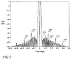
- the side lobe levels of the piecewise linear delta antenna pattern 310 may be a close approximation to that corresponding to 40 dB Bayliss-Taylor weights, with the exception of a small number of lobes, referred to as grating lobes 315, that are higher in the antenna pattern resulting from piecewise linear weights than in the antenna pattern resulting from Bayliss-Taylor weights.
- the antenna patterns illustrated in FIG. 3 are calculated for 128 antenna elements, in 8 sub-arrays (with 16 elements per sub-array), i.e., the piecewise linear weighting function is composed of 8 linear segments.
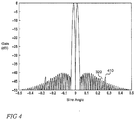
- an antenna pattern 410 resulting from piecewise linear weights formed over an antenna with 128 elements in 16 sub-arrays has significantly attenuated grating lobes compared to the antenna pattern 310 of FIG.3 , resulting from piecewise linear weights formed over an antenna with 128 elements in 8 sub-arrays.
- the sidelobe levels of the antenna pattern 410 of FIG. 4 are at nearly all angles approximately 7.5 dB lower than those for an antenna pattern resulting from derivative weights.
- Embodiments of the present invention may be used to provide two delta signals, e.g., an azimuth delta signal and an elevation delta signal, simultaneously, by processing azimuth arrays and elevation arrays in parallel.
- an analog processor 155 is fabricated as a printed wiring board with a layout as shown.
- the analog processor has a sum input 510 and two delta inputs, an elevation delta input 515, and an azimuth delta input 520.
- the sum input 510 also functions, when the antenna is transmitting, as a transmit output; separation of received and transmitted signals is accomplished by the circulator 525.
- Isolators 530 each of which may be a circulator with a terminated terminal, are used for isolation throughout the circuit.
- Low-noise amplifiers (LNAs) 535 are used to amplify the received signals, and a power amplifier 540, under the control of a control circuit 545, is used to amplify the transmitted signal.
- the analog processor 155 has a sum output 550, an elevation delta output 555, and an azimuth delta output 560.
- the sum output 550 also serves as a transmit input for receiving a signal to be transmitted when the antenna is operating in transmit mode.
- Each gain-phase modules 160a - 160c implemented as monolithic microwave integrated circuits (MMICs) referred to as common leg circuits (CLCs), provide gain and phase control.
- MMICs monolithic microwave integrated circuits
- CLCs common leg circuits
- an LNA 535 amplifies the signal received by the analog processor 155 at the elevation delta input 515
- an inline gain-phase module 160b adjusts the gain and phase of the signal, which then propagates through an isolator 530 to a cross combiner 162.
- the signal at the sum input 510 is amplified by an LNA 535, is split, and propagates through three isolators 530.
- a cross gain-phase module 160a then adjusts the gain and phase of one of these three signals, which then propagates through an isolator 530, to be added to the processed elevation delta signal by the cross combiner 162.
- the azimuth delta signal is processed similarly by a respective LNA 535, respective isolators 530, and a respective inline gain-phase module 160b, and it is combined with a second one of the three sum signals resulting from splitting after the LNA 535 in the sum signal path.
- the third one of the three sum signals resulting from splitting after the LNA 535 in the sum signal path is processed by a sum gain-phase module 160c, and routed to the sum output 550 of the analog processor 155.
Landscapes
- Engineering & Computer Science (AREA)
- Radar, Positioning & Navigation (AREA)
- Remote Sensing (AREA)
- Computer Networks & Wireless Communication (AREA)
- Physics & Mathematics (AREA)
- General Physics & Mathematics (AREA)
- Variable-Direction Aerials And Aerial Arrays (AREA)
Description
- One or more aspects of embodiments according to the present invention relate to monopulse radar, and more particularly to a system and method for forming a monopulse radar delta beam using piecewise-linear weights.
- Monopulse radar systems illuminate a target and receive the radar return with several different receiving antenna patterns, referred to as a sum beam, and one or more delta beams. A delta beam may have an antenna pattern with a null and phase reversal in the center of the pattern, so that the magnitude of the return in the delta beam provides a measure of the magnitude of the misalignment between the line of sight to the target and the center of the delta beam, and the phase of the delta beam return relative to the phase of the sum beam return provides an indication of the direction in which the line of sight to the target is misaligned with the center of the delta beam. Two delta beams may be used, one to measure misalignment in azimuth, for example, and one to measure misalignment in elevation.
- A monopulse radar antenna may be an array antenna composed of a number of sub-arrays installed side by side, with a set of array element weights for each beam. The sum beam may be formed with a set of weights referred to as the sum weights, and a delta beam may be formed by applying an additional set of weights, referred to as the delta over sum (D/S) weights, so that each weight used in forming the delta beam is the product of a sum weight and a delta over sum weight. In related art systems, the delta over sum weights may differ from sub-array to sub-array, resulting in high manufacturing and maintenance costs associated with fabricating and maintaining a large number of distinct parts. In one related art approach, the sub-arrays are made identical and the delta over sum weights increase linearly across the array, with a single programmable weight per sub-array being the only difference between sub-arrays. This approach results in a reduction in manufacturing and maintenance costs, but these benefits are obtained at a cost in performance, e.g., in higher sidelobe levels (SLL).
- Thus, there is a need for a monopulse radar system that provides good performance, and is constructed using identical sub-arrays. A modular constrained feed for low sidelobe array is known from
US5216428A . An antenna device is known fromJP2012175469A US4642645A . An array beamformer using unequal power couplers for plural beams is known fromUS5166690A . A Ku Band Linear Phased Array is known from: JABUS BARKER ET AL, "Ku Band Linear Phased Array", MICROWAVE J,, (19771001), vol. 20, no. 10, pages 44 - 46, XP001387307 [A] 1,3,5,7,8,10-20 * Sections "Antenna Design" and "Subarray Design"; page 44 - page 46. - In accordance with the present invention, there is provided a beam former as defined by
claim 1. - Features, aspects, and embodiments are described in conjunction with the attached drawings, in which:
-
FIG. 1 is a block diagram of an array antenna and beam former according to an embodiment of the present invention; -
FIG. 2A is a graph of Bayliss-Taylor weights and of a piecewise-linear approximation to Bayliss-Taylor weights, according to an embodiment of the present invention; -
FIG. 2B is a graph of gain-phase module gain settings for two sets of gain-phase modules, used to form the piecewise linear weights ofFIG. 2A , in one embodiment of the present invention; -
FIG. 3 is a graph of a delta antenna pattern formed using Bayliss-Taylor weights and a delta antenna pattern formed using a piecewise linear approximation to Bayliss-Taylor weights over 8 sub-arrays, according to an embodiment of the present invention; -
FIG. 4 is a graph of a delta antenna pattern formed using Bayliss-Taylor weights and a delta antenna pattern formed using a piecewise linear approximation to Bayliss-Taylor weights over 16 sub-arrays, according to an embodiment of the present invention; and -
FIG. 5 is a printed wiring board layout of an analog processor according to an embodiment of the present invention. - The detailed description set forth below in connection with the appended drawings is intended as a description of exemplary embodiments of an electronically reconfigurable, piecewise-linear, scalable analog monopulse network provided in accordance with the present invention and is not intended to represent the only forms in which the present invention may be constructed or utilized. The description sets forth the features of the present invention in connection with the illustrated embodiments. It is to be understood, however, that the same or equivalent functions and structures may be accomplished by different embodiments that are also intended to be encompassed within the spirit and scope of the invention. As denoted elsewhere herein, like element numbers are intended to indicate like elements or features.
- Referring to
FIG. 1 , in one embodiment afirst sub-array 110 of antenna elements and asecond sub-array 115 of antenna elements are part of an array, which may include additional sub-arrays, Signals received at eachantenna element output 122 are amplified and phase shifted by anelement gain block 123 and fed to acoupler 125, at acoupler input 124. The signal at thecoupler input 124 is split, by thecoupler 125, into a sum beam contribution, at the output port of thecoupler 125, and adelta beam contribution 126, at the coupled port of thecoupler 125. The sum beam contributions are added in asub-array sum combiner 130, which may for example be a corporate feed network with multiple 2:1 combiners, to form theoutput 135 of the sum feed network. The amplitude of the ithdelta beam contribution 126 is proportional to the coupling coefficient bi in thecorresponding coupler 125. The delta beam contributions are added in asub-array delta combiner 145, which may for example be a corporate feed network with multiple 2:1 combiners, to form theoutput 150 of the delta feed network. - As used herein, the "delta feed network" is the network that has, as inputs, the plurality of
coupler inputs 124, and that has a single output, theoutput 150 of the delta feed network. As used herein, the "sum feed network" is the network that has the plurality ofantenna element outputs 122 as inputs and a single output, theoutput 135 of the sum feed network. Thus, the delta feed network and the sum feed network both include the couplers, as shared elements. As used herein terminals of two elements are "connected" if they are directly or indirectly connected. For example, each coupledport 126 is connected to a respective antenna element through arespective coupler 125 and through a respectiveelement gain block 123. - The
output 135 of the sum feed network and theoutput 150 of the delta feed network are fed into respective inputs of ananalog processor 155, the inputs being referred to herein as the sum input and the delta input, respectively, of theanalog processor 155. Within the analog processor, gain-phase modules FIG. 1 , a portion of the signal at the sum input of theanalog processor 155 is split off by a power divider 161 (illustrated as a tee) and this portion is processed by a gain-phase module 160a, referred to herein as a cross gain-phase module 160a. The remainder of the signal at the sum input of theanalog processor 155 forms the signal at an output, referred to as the sum output, of theanalog processor 155. The signal at the delta input of theanalog processor 155 is processed by another gain-phase module 160b, referred to herein as an inline gain-phase module 160b and the outputs of the cross gain-phase module 160a and the inline gain-phase module 160b are added, i.e., combined, in a power combiner referred to as across combiner 162, to form the signal at an output of theanalog processor 155, referred to as theprocessor delta output 163. In one embodiment the cross gain-phase module 160a and the inline gain-phase module 160b are electronically adjustable, each containing a non-transitory digital storage medium (e.g., volatile or non-volatile random-access memory (RAM), or an array of flip-flops) storing a first digital number, which determines the gain setting of the gain-phase module phase module - The sum outputs of the
analog processors 155, each associated with a sub-array of the array, are, in one embodiment, added in an array sum combiner 164 to form thearray sum output 165, and the delta outputs of theanalog processors 155 associated with all of the sub-arrays in the array are added in an array delta combiner 170 to form thearray delta output 175. Each of the array sum combiner 164 and thearray delta combiner 170 may for example be a corporate feed network with multiple 2:1 combiners. - The circuitry connecting the antenna elements of the
first sub-array 110 or thesecond sub-array 115 to the sum output of the correspondinganalog processor 155 is referred to herein as the first or second sub-array sum beam former, respectively, The circuitry connecting the antenna elements of thefirst sub-array 110 or thesecond sub-array 115 to the correspondingprocessor delta output 163 is referred to herein as the first or second sub-array delta beam former, respectively. The circuitry connecting the antenna elements of thefirst sub-array 110 and of thesecond sub-array 115 to thearray sum output 165 is referred to herein as the sum beam former, and the circuitry connecting the antenna elements of thefirst sub-array 110 and of thesecond sub-array 115 to thearray delta output 175 is referred to herein as the delta beam former. The combination of the sum beam former and the delta beam former is referred to herein as the beam former. - The signal at the
array sum output 165 is a linear combination, i.e., a weighted sum, of theelement outputs 122, and the gain from each of theelement outputs 122 to thearray sum output 165 may be referred to as a sum weight. Similarly, the gain from each of theelement outputs 122 to thearray delta output 175 may be referred to as a delta weight. The delta weights include the gains of theelement gain blocks 123, which are used to form and steer the sum beam. The delta weights differ from the sum weights as a result of contributions from, e.g., the coupling coefficients bi, the gains of the cross gain-phase modules 160a, and the inline gain-phase modules 160b. The ratios of the delta weights to the respective sum weights may be referred to as the delta over sum weights, or D/S weights. - In one embodiment the
couplers 125 are designed so that their respective coupling coefficients increase linearly with position across the sub-array, i.e., so that the gain from thecoupler input 124 to theprocessor delta output 163 differs, for any pair of adjacent antenna elements, by a gain increment, which is the same for each pair of adjacent antenna elements. Consequently the D/S weights also vary linearly, with the gain increment, across the sub-array. The gain increment is proportional to the gain of the inline gain-phase module 160b, and it may be positive or negative depending on the phase setting of the inline gain-phase module 160b. The inline gain-phase module 160b may have a nominal setting, e.g., a gain setting that is at the midpoint of the range of gain settings available in the inline gain-phase module 160b. The gain increment corresponding to the nominal gain setting of the gain-phase module 160b is referred to herein as the nominal gain increment. - If the coupling coefficients of the
couplers 125 increase linearly with position across each sub-array, then the gain settings of the cross gain-phase modules 160a may be selected to cause the gain to increase linearly across the entire array. In particular, this may be done by selecting the gains of the cross gain-phase modules 160a to increase linearly across the array in the same direction as the direction in which the coupling coefficients increase linearly with position across the sub-array, with the gain of each cross gain-phase module 160a differing from the gain of the cross gain-phase module 160a of an adjacent sub-array by N times the gain increment, where N is the number of elements in each sub-array. In this antenna configuration, the gains of the inline gain-phase modules 160b may be set to one, or to a uniform value that is the same for all sub-arrays, or they may be adjusted to compensate for differences between the sub-arrays resulting, for example, from non-uniformity or imperfections in the manufacturing process. For example, if as a result of such imperfections the nominal gain increment of thefirst sub-array 110 is greater, by some ratio, than the nominal gain increment of thesecond sub-array 115, the gain of the inline gain-phase module 160b corresponding to thefirst sub-array 110 may be made less than the gain of the inline gain-phase module 160b corresponding to thesecond sub-array 115 by the same ratio, to compensate for the imperfections. This set of delta over sum weights, referred to herein as derivative weights, which increase linearly across the entire array, may be used to form a delta antenna pattern, but it may result in undesirable beam characteristics, e.g., side lobe levels (SLLs) that are higher than desired. - In one embodiment, the gains of the cross gain-
phase modules 160a and of the inline gain-phase modules 160b may be selected to form a D/S weight profile across the array that is piecewise linear. As used herein, the term piecewise linear refers to a function that is composed of at least two linear segments, with at least two of the segments not being colinear, e.g., having a substantially different slope. In one embodiment, the slope between a pair of segments in the piecewise linear D/S weight profile across the array may differ by at least 2 dB. Referring toFIGs. 2A and 2B , in this embodiment, the D/S weights may form a piecewiselinear function 205 approximating a desired D/S weighting function 210, which may for example be a Bayliss-Taylor D/S weighting function, known to those of skill in the art as a weighting function producing a low SLL for a given beam width. The piecewiselinear function 205 may for example be implemented using gains shown inFIG. 2B . InFIG. 2B , afirst curve 215 shows suitable gains for the cross gain-phase modules 160a and asecond curve 220 shows suitable gains for the inline gain-phase modules 160b, for achieving the piecewise-linear weight profile ofFIG. 2A . A negative gains, i.e., a gain less than 0, may be achieved by selecting a phase setting in a cross gain-phase module 160a or an inline gain-phase module 160b that differs by 180 degrees from the phase setting of a corresponding cross gain-phase module 160a or inline gain-phase module 160b with positive gain. It may be advantageous to use a D/S weight profile that is both piecewise linear and continuous, so that the D/S weight for an antenna element at the edge of a first sub-array configured with a slope corresponding to a first gain increment differs from the D/S weight for an adjacent antenna element at the edge of an adjacent sub-array configured with a slope corresponding to a second gain increment, by an amount less than or substantially equal to the larger of the two gain increments. - Referring to
FIG. 3 , the side lobe levels of the piecewise lineardelta antenna pattern 310 may be a close approximation to that corresponding to 40 dB Bayliss-Taylor weights, with the exception of a small number of lobes, referred to as gratinglobes 315, that are higher in the antenna pattern resulting from piecewise linear weights than in the antenna pattern resulting from Bayliss-Taylor weights. The antenna patterns illustrated inFIG. 3 are calculated for 128 antenna elements, in 8 sub-arrays (with 16 elements per sub-array), i.e., the piecewise linear weighting function is composed of 8 linear segments. - Referring to
FIG. 4 , anantenna pattern 410 resulting from piecewise linear weights formed over an antenna with 128 elements in 16 sub-arrays (with 8 elements per sub-array) has significantly attenuated grating lobes compared to theantenna pattern 310 ofFIG.3 , resulting from piecewise linear weights formed over an antenna with 128 elements in 8 sub-arrays. The sidelobe levels of theantenna pattern 410 ofFIG. 4 , resulting from piecewise linear weights, are at nearly all angles approximately 7.5 dB lower than those for an antenna pattern resulting from derivative weights. - Embodiments of the present invention may be used to provide two delta signals, e.g., an azimuth delta signal and an elevation delta signal, simultaneously, by processing azimuth arrays and elevation arrays in parallel. Referring to
FIG. 5 , in one embodiment ananalog processor 155 is fabricated as a printed wiring board with a layout as shown. The analog processor has asum input 510 and two delta inputs, anelevation delta input 515, and anazimuth delta input 520. In the embodiment ofFIG. 5 , thesum input 510 also functions, when the antenna is transmitting, as a transmit output; separation of received and transmitted signals is accomplished by thecirculator 525.Isolators 530, each of which may be a circulator with a terminated terminal, are used for isolation throughout the circuit. Low-noise amplifiers (LNAs) 535 are used to amplify the received signals, and apower amplifier 540, under the control of acontrol circuit 545, is used to amplify the transmitted signal. Theanalog processor 155 has asum output 550, anelevation delta output 555, and anazimuth delta output 560. Thesum output 550 also serves as a transmit input for receiving a signal to be transmitted when the antenna is operating in transmit mode. - Five gain-
phase modules 160a - 160c, implemented as monolithic microwave integrated circuits (MMICs) referred to as common leg circuits (CLCs), provide gain and phase control. In the elevation delta signal path, anLNA 535 amplifies the signal received by theanalog processor 155 at theelevation delta input 515, and an inline gain-phase module 160b adjusts the gain and phase of the signal, which then propagates through anisolator 530 to across combiner 162. The signal at thesum input 510 is amplified by anLNA 535, is split, and propagates through threeisolators 530. A cross gain-phase module 160a then adjusts the gain and phase of one of these three signals, which then propagates through anisolator 530, to be added to the processed elevation delta signal by thecross combiner 162. The azimuth delta signal is processed similarly by arespective LNA 535,respective isolators 530, and a respective inline gain-phase module 160b, and it is combined with a second one of the three sum signals resulting from splitting after theLNA 535 in the sum signal path. The third one of the three sum signals resulting from splitting after theLNA 535 in the sum signal path is processed by a sum gain-phase module 160c, and routed to thesum output 550 of theanalog processor 155. - Although limited embodiments of an electronically reconfigurable, piecewise-linear, scalable analog monopulse network have been specifically described and illustrated herein, many modifications and variations will be apparent to those skilled in the art. Accordingly, it is to be understood that an electronically reconfigurable, piecewise-linear, scalable analog monopulse network employed according to principles of this invention may be embodied other than as specifically described herein. The invention is defined in the following claims.
Claims (14)
- A beam former for monopulse beam forming in a phased array antenna comprising a first sub-array (110) comprising a first plurality of antenna elements and a second sub-array (115) comprising a second plurality of antenna elements, the beam former comprising:a sum beam former (165) connected to the first plurality of antenna elements and the second plurality of antenna elements, and comprising an array sum output,a first delta sub-array beam former comprising:a first delta feed network connected to the first plurality of antenna elements; anda first inline gain-phase module (160b) connected to an output of the first delta feed network,the first delta sub-array beam former being configured to provide a first plurality of delta over sum, D/S, weights with respect to the sum beam former, the first plurality of D/S weights varying substantially linearly, with a first gain increment, across the first sub-array;a second delta sub-array beam former comprising:a second delta feed network connected to the second plurality of antenna elements; anda second inline gain-phase module (160b) connected to an output of the second delta feed network,the second delta sub-array beam former being configured to provide a second plurality of D/S weights with respect to the sum beam former, the second plurality of D/S weights varying substantially linearly, with a second gain increment, across the second sub-array;the first and second inline gain-phase modules being configured to provide a first gain increment and a second gain increment differing by at least 2 decibels, dB, wherein:the first sub-array and the second sub-array are adjacent sub-arrays of the phased array;the sum beam former comprises a first sub-array sum beam former (130) and a second sub-array sum beam former (130) connected to the first sub-array and the second sub-array respectively; characterized in that,the beam former further comprises:a first cross gain-phase module (160a) connected to an output of the first sub-array sum beam former and to a first cross combiner, the first cross combiner configured to add the output of the first cross gain-phase module and the output of the first inline gain-phase module; anda second cross gain-phase module (160a) connected to an output of the second sub-array sum beam former and to a second cross combiner, the second cross combiner configured to add the output of the second cross gain-phase module and the output of the second inline gain-phase module;the first inline gain-phase module, the second inline gain-phase module, the first cross gain-phase module and the second cross gain-phase module configured to provide:a D/S weight for a first antenna element, differing froma D/S weight for a second antenna element adjacent to the first antenna element in the phased array antennaby an amount less than the first gain increment and less than the second gain increment.
- The beam former of claim 1, wherein the first inline gain-phase module is a monolithic microwave integrated circuit, MMIC, and the second inline gain-phase module is a MMIC.
- The beam former of claim 2, wherein the first cross gain-phase module is a MMIC and the second cross gain-phase module is a MMIC.
- The beam former of claim 2, wherein each of:the first inline gain-phase module;the second inline gain-phase module;the first cross gain-phase module; andthe second cross gain-phase modulecomprises a phase shifter, for applying a phase change to a signal propagating through the gain-phase module.
- The beam former of claim 4, wherein each phase shifter comprises a non-transitory digital storage medium storing a phase setting, the gain-phase module comprising the phase shifter configured to apply a phase change corresponding to the phase setting to a signal propagating through the gain-phase module.
- The beam former of claim 5, wherein the difference between the phase setting of the first inline gain-phase module and the phase setting of the second inline gain-phase module corresponds to substantially 180 degrees of phase.
- The beam former of claim 2, wherein each of:the first inline gain-phase module;the second inline gain-phase module;the first cross gain-phase module; andthe second cross gain-phase modulecomprises a gain control, for applying a gain change to a signal propagating through the gain-phase module.
- The beam former of claim 7 wherein each gain control comprises a non-transitory digital storage medium storing a gain setting, the gain-phase module comprising the gain control being configured to apply a gain change corresponding to the gain setting to a signal propagating through the gain-phase module.
- The beam former of claim 2, wherein:the first inline gain-phase module;the second inline gain-phase module;the first cross gain-phase module; andthe second cross gain-phase moduleare configured to provide a plurality of D/S weights that form a piecewise-linear approximation to a desired weighting function.
- The beam former of claim 2, wherein:the sum beam former comprises a first sum feed network connected to the first plurality of antenna elements; andthe beam former comprises a first analog processor, the first analog processor comprising:the first inline gain-phase module;the first cross gain-phase module;a sum input connected to a first sum feed network;a delta input connected to the first delta feed network;a sum output; anda delta output.
- The beam former of claim 10, wherein the first analog processor comprises:a low-noise amplifier connected to the sum input, and configured to amplify a signal received by the analog processor at the sum input; anda low-noise amplifier connected to the delta input, and configured to amplify a signal received by the analog processor at the delta input.
- The beam former of claim 10, wherein the first analog processor comprises a transmit signal path.
- The beam former of claim 1, wherein the first delta feed network comprises a plurality of couplers, each of the plurality of couplers connected to a respective antenna element of the plurality of antenna elements of the first sub-array.
- The beam former of claim 13, wherein each of the plurality of couplers has a coupling coefficient, the coupling coefficients increasing linearly with the position of corresponding antenna elements in the first sub-array.
Applications Claiming Priority (2)
| Application Number | Priority Date | Filing Date | Title |
|---|---|---|---|
| US14/341,648 US9502766B2 (en) | 2014-07-25 | 2014-07-25 | Electronically reconfigurable, piecewise-linear, scalable analog monopulse network |
| PCT/US2015/036838 WO2016014188A1 (en) | 2014-07-25 | 2015-06-20 | Electronically reconfigurable, piecewise-linear, scalable analog monopulse feeding network |
Publications (2)
| Publication Number | Publication Date |
|---|---|
| EP3172799A1 EP3172799A1 (en) | 2017-05-31 |
| EP3172799B1 true EP3172799B1 (en) | 2019-03-27 |
Family
ID=53525275
Family Applications (1)
| Application Number | Title | Priority Date | Filing Date |
|---|---|---|---|
| EP15735797.1A Active EP3172799B1 (en) | 2014-07-25 | 2015-06-20 | Electronically reconfigurable, piecewise-linear, scalable analog monopulse feeding network |
Country Status (3)
| Country | Link |
|---|---|
| US (1) | US9502766B2 (en) |
| EP (1) | EP3172799B1 (en) |
| WO (1) | WO2016014188A1 (en) |
Families Citing this family (6)
| Publication number | Priority date | Publication date | Assignee | Title |
|---|---|---|---|---|
| US10288715B2 (en) | 2016-09-09 | 2019-05-14 | Raytheon Company | Systems and methods for direction finding using augmented spatial sample covariance matrices |
| US10768265B2 (en) * | 2016-11-09 | 2020-09-08 | Raytheon Company | Systems and methods for direction finding using compressive sensing |
| CN108051782B (en) * | 2017-11-22 | 2021-06-15 | 西南电子技术研究所(中国电子科技集团公司第十研究所) | Large-scale phased array difference beam forming system based on subarray division |
| CN108199152B (en) * | 2017-12-14 | 2020-07-14 | 安徽四创电子股份有限公司 | Design method of large low-sidelobe level array antenna feed network |
| WO2021259203A1 (en) | 2020-06-22 | 2021-12-30 | 正大天晴药业集团股份有限公司 | Preparation method for cdk4/6 inhibitor |
| CN115117626B (en) * | 2021-03-22 | 2024-09-13 | 广州视源电子科技股份有限公司 | Antenna assembly, screen transmitter and screen throwing system |
Family Cites Families (16)
| Publication number | Priority date | Publication date | Assignee | Title |
|---|---|---|---|---|
| US5216428A (en) | 1984-05-16 | 1993-06-01 | Hughes Aircraft Company | Modular constrained feed for low sidelobe array |
| US4642645A (en) | 1985-05-07 | 1987-02-10 | The United States Of America As Represented By The Secretary Of The Air Force | Reducing grating lobes due to subarray amplitude tapering |
| US5017927A (en) * | 1990-02-20 | 1991-05-21 | General Electric Company | Monopulse phased array antenna with plural transmit-receive module phase shifters |
| US5600326A (en) * | 1991-12-16 | 1997-02-04 | Martin Marietta Corp. | Adaptive digital beamforming architecture and algorithm for nulling mainlobe and multiple sidelobe radar jammers while preserving monopulse ratio angle estimation accuracy |
| US5166690A (en) | 1991-12-23 | 1992-11-24 | Raytheon Company | Array beamformer using unequal power couplers for plural beams |
| US5274384A (en) * | 1992-12-28 | 1993-12-28 | General Electric Company | Antenna beamformer |
| US6483478B2 (en) * | 2001-01-31 | 2002-11-19 | Lockheed Martin Corporation | Monopulse array radar with single difference beam for simultaneous azimuth and elevation angle determination |
| US20030184473A1 (en) * | 2002-03-27 | 2003-10-02 | Yu Kai Bor | Adaptive digital sub-array beamforming and deterministic sum and difference beamforming, with jamming cancellation and monopulse ratio preservation |
| US6661366B2 (en) * | 2001-06-15 | 2003-12-09 | Lockheed Martin Corporation | Adaptive digital sub-array beamforming and deterministic sum and difference beamforming, with jamming cancellation and monopulse ratio preservation |
| US6697009B2 (en) * | 2001-06-15 | 2004-02-24 | Lockheed Martin Corporation | Adaptive digital beamforming architecture for target detection and angle estimation in multiple mainlobe and sidelobe jamming |
| US6720910B2 (en) * | 2001-08-16 | 2004-04-13 | Lockheed Martin Corporation | Pri-staggered post-doppler adaptive monopulse processing for detection and location of a moving target in ground clutter |
| US6930637B2 (en) * | 2001-11-15 | 2005-08-16 | Texas Instruments Incorporated | Method and apparatus for high resolution tracking via mono-pulse beam-forming in a communication system |
| US7671789B1 (en) * | 2008-10-03 | 2010-03-02 | Lockheed Martin Corporation | Method and system for target detection and angle estimation based on a radar signal |
| US8427371B2 (en) | 2010-04-09 | 2013-04-23 | Raytheon Company | RF feed network for modular active aperture electronically steered arrays |
| JP5665595B2 (en) | 2011-02-22 | 2015-02-04 | 三菱電機株式会社 | Antenna device |
| US9124361B2 (en) | 2011-10-06 | 2015-09-01 | Raytheon Company | Scalable, analog monopulse network |
-
2014
- 2014-07-25 US US14/341,648 patent/US9502766B2/en active Active
-
2015
- 2015-06-20 EP EP15735797.1A patent/EP3172799B1/en active Active
- 2015-06-20 WO PCT/US2015/036838 patent/WO2016014188A1/en not_active Ceased
Non-Patent Citations (1)
| Title |
|---|
| None * |
Also Published As
| Publication number | Publication date |
|---|---|
| US20160028155A1 (en) | 2016-01-28 |
| WO2016014188A1 (en) | 2016-01-28 |
| EP3172799A1 (en) | 2017-05-31 |
| US9502766B2 (en) | 2016-11-22 |
Similar Documents
| Publication | Publication Date | Title |
|---|---|---|
| US9502766B2 (en) | Electronically reconfigurable, piecewise-linear, scalable analog monopulse network | |
| AU2011238848B2 (en) | An RF feed network for modular active aperture electronically steered arrays | |
| AU2012319035B2 (en) | Scalable, analog monopulse network | |
| EP4135125B1 (en) | Phased array antenna system | |
| US5166690A (en) | Array beamformer using unequal power couplers for plural beams | |
| JP2629057B2 (en) | Self-monitoring and calibration phased array radar | |
| US6356233B1 (en) | Structure for an array antenna, and calibration method therefor | |
| Akbar et al. | Scalable phased array architectures with a reduced number of tunable phase shifters | |
| JP2013529411A5 (en) | ||
| JP2010252188A (en) | Array antenna device | |
| US20160093958A1 (en) | Negative group delay circuit | |
| USH1773H (en) | Ultra-wideband active electronically scanned antenna | |
| Akbar et al. | Design of a scalable phased array antenna with a simplified architecture | |
| JP6185767B2 (en) | Phased array power feeding device and phased array antenna device | |
| KR102010303B1 (en) | Phased array antenna | |
| WO2021106003A1 (en) | Metal waveguide connected antenna array | |
| Duffy et al. | Integrated compensation network for low mutual coupling of planar microstrip antenna arrays | |
| WO2018201223A1 (en) | Reducing beamwidth dispersion and improving pattern quality for antenna arrays | |
| Gresham | ‘An AESA revolution utilizing the disruptive technology of highly-integrated silicon ICs | |
| CN121011855A (en) | Ku-band dual-band common-aperture active phased array transceiver antenna array and antenna system | |
| JP5792669B2 (en) | Array antenna device |
Legal Events
| Date | Code | Title | Description |
|---|---|---|---|
| STAA | Information on the status of an ep patent application or granted ep patent |
Free format text: STATUS: THE INTERNATIONAL PUBLICATION HAS BEEN MADE |
|
| PUAI | Public reference made under article 153(3) epc to a published international application that has entered the european phase |
Free format text: ORIGINAL CODE: 0009012 |
|
| STAA | Information on the status of an ep patent application or granted ep patent |
Free format text: STATUS: REQUEST FOR EXAMINATION WAS MADE |
|
| 17P | Request for examination filed |
Effective date: 20170127 |
|
| AK | Designated contracting states |
Kind code of ref document: A1 Designated state(s): AL AT BE BG CH CY CZ DE DK EE ES FI FR GB GR HR HU IE IS IT LI LT LU LV MC MK MT NL NO PL PT RO RS SE SI SK SM TR |
|
| AX | Request for extension of the european patent |
Extension state: BA ME |
|
| DAV | Request for validation of the european patent (deleted) | ||
| DAX | Request for extension of the european patent (deleted) | ||
| STAA | Information on the status of an ep patent application or granted ep patent |
Free format text: STATUS: EXAMINATION IS IN PROGRESS |
|
| 17Q | First examination report despatched |
Effective date: 20180312 |
|
| GRAP | Despatch of communication of intention to grant a patent |
Free format text: ORIGINAL CODE: EPIDOSNIGR1 |
|
| STAA | Information on the status of an ep patent application or granted ep patent |
Free format text: STATUS: GRANT OF PATENT IS INTENDED |
|
| INTG | Intention to grant announced |
Effective date: 20181011 |
|
| GRAS | Grant fee paid |
Free format text: ORIGINAL CODE: EPIDOSNIGR3 |
|
| GRAA | (expected) grant |
Free format text: ORIGINAL CODE: 0009210 |
|
| STAA | Information on the status of an ep patent application or granted ep patent |
Free format text: STATUS: THE PATENT HAS BEEN GRANTED |
|
| AK | Designated contracting states |
Kind code of ref document: B1 Designated state(s): AL AT BE BG CH CY CZ DE DK EE ES FI FR GB GR HR HU IE IS IT LI LT LU LV MC MK MT NL NO PL PT RO RS SE SI SK SM TR |
|
| REG | Reference to a national code |
Ref country code: GB Ref legal event code: FG4D |
|
| REG | Reference to a national code |
Ref country code: CH Ref legal event code: EP |
|
| REG | Reference to a national code |
Ref country code: AT Ref legal event code: REF Ref document number: 1114142 Country of ref document: AT Kind code of ref document: T Effective date: 20190415 |
|
| REG | Reference to a national code |
Ref country code: IE Ref legal event code: FG4D |
|
| REG | Reference to a national code |
Ref country code: DE Ref legal event code: R096 Ref document number: 602015027152 Country of ref document: DE |
|
| PG25 | Lapsed in a contracting state [announced via postgrant information from national office to epo] |
Ref country code: SE Free format text: LAPSE BECAUSE OF FAILURE TO SUBMIT A TRANSLATION OF THE DESCRIPTION OR TO PAY THE FEE WITHIN THE PRESCRIBED TIME-LIMIT Effective date: 20190327 Ref country code: NO Free format text: LAPSE BECAUSE OF FAILURE TO SUBMIT A TRANSLATION OF THE DESCRIPTION OR TO PAY THE FEE WITHIN THE PRESCRIBED TIME-LIMIT Effective date: 20190627 Ref country code: LT Free format text: LAPSE BECAUSE OF FAILURE TO SUBMIT A TRANSLATION OF THE DESCRIPTION OR TO PAY THE FEE WITHIN THE PRESCRIBED TIME-LIMIT Effective date: 20190327 Ref country code: FI Free format text: LAPSE BECAUSE OF FAILURE TO SUBMIT A TRANSLATION OF THE DESCRIPTION OR TO PAY THE FEE WITHIN THE PRESCRIBED TIME-LIMIT Effective date: 20190327 |
|
| REG | Reference to a national code |
Ref country code: NL Ref legal event code: MP Effective date: 20190327 |
|
| PG25 | Lapsed in a contracting state [announced via postgrant information from national office to epo] |
Ref country code: GR Free format text: LAPSE BECAUSE OF FAILURE TO SUBMIT A TRANSLATION OF THE DESCRIPTION OR TO PAY THE FEE WITHIN THE PRESCRIBED TIME-LIMIT Effective date: 20190628 Ref country code: BG Free format text: LAPSE BECAUSE OF FAILURE TO SUBMIT A TRANSLATION OF THE DESCRIPTION OR TO PAY THE FEE WITHIN THE PRESCRIBED TIME-LIMIT Effective date: 20190627 Ref country code: NL Free format text: LAPSE BECAUSE OF FAILURE TO SUBMIT A TRANSLATION OF THE DESCRIPTION OR TO PAY THE FEE WITHIN THE PRESCRIBED TIME-LIMIT Effective date: 20190327 Ref country code: RS Free format text: LAPSE BECAUSE OF FAILURE TO SUBMIT A TRANSLATION OF THE DESCRIPTION OR TO PAY THE FEE WITHIN THE PRESCRIBED TIME-LIMIT Effective date: 20190327 Ref country code: HR Free format text: LAPSE BECAUSE OF FAILURE TO SUBMIT A TRANSLATION OF THE DESCRIPTION OR TO PAY THE FEE WITHIN THE PRESCRIBED TIME-LIMIT Effective date: 20190327 Ref country code: LV Free format text: LAPSE BECAUSE OF FAILURE TO SUBMIT A TRANSLATION OF THE DESCRIPTION OR TO PAY THE FEE WITHIN THE PRESCRIBED TIME-LIMIT Effective date: 20190327 |
|
| REG | Reference to a national code |
Ref country code: AT Ref legal event code: MK05 Ref document number: 1114142 Country of ref document: AT Kind code of ref document: T Effective date: 20190327 |
|
| PG25 | Lapsed in a contracting state [announced via postgrant information from national office to epo] |
Ref country code: SK Free format text: LAPSE BECAUSE OF FAILURE TO SUBMIT A TRANSLATION OF THE DESCRIPTION OR TO PAY THE FEE WITHIN THE PRESCRIBED TIME-LIMIT Effective date: 20190327 Ref country code: IT Free format text: LAPSE BECAUSE OF FAILURE TO SUBMIT A TRANSLATION OF THE DESCRIPTION OR TO PAY THE FEE WITHIN THE PRESCRIBED TIME-LIMIT Effective date: 20190327 Ref country code: RO Free format text: LAPSE BECAUSE OF FAILURE TO SUBMIT A TRANSLATION OF THE DESCRIPTION OR TO PAY THE FEE WITHIN THE PRESCRIBED TIME-LIMIT Effective date: 20190327 Ref country code: EE Free format text: LAPSE BECAUSE OF FAILURE TO SUBMIT A TRANSLATION OF THE DESCRIPTION OR TO PAY THE FEE WITHIN THE PRESCRIBED TIME-LIMIT Effective date: 20190327 Ref country code: AL Free format text: LAPSE BECAUSE OF FAILURE TO SUBMIT A TRANSLATION OF THE DESCRIPTION OR TO PAY THE FEE WITHIN THE PRESCRIBED TIME-LIMIT Effective date: 20190327 Ref country code: PT Free format text: LAPSE BECAUSE OF FAILURE TO SUBMIT A TRANSLATION OF THE DESCRIPTION OR TO PAY THE FEE WITHIN THE PRESCRIBED TIME-LIMIT Effective date: 20190727 Ref country code: CZ Free format text: LAPSE BECAUSE OF FAILURE TO SUBMIT A TRANSLATION OF THE DESCRIPTION OR TO PAY THE FEE WITHIN THE PRESCRIBED TIME-LIMIT Effective date: 20190327 Ref country code: ES Free format text: LAPSE BECAUSE OF FAILURE TO SUBMIT A TRANSLATION OF THE DESCRIPTION OR TO PAY THE FEE WITHIN THE PRESCRIBED TIME-LIMIT Effective date: 20190327 |
|
| PG25 | Lapsed in a contracting state [announced via postgrant information from national office to epo] |
Ref country code: SM Free format text: LAPSE BECAUSE OF FAILURE TO SUBMIT A TRANSLATION OF THE DESCRIPTION OR TO PAY THE FEE WITHIN THE PRESCRIBED TIME-LIMIT Effective date: 20190327 Ref country code: PL Free format text: LAPSE BECAUSE OF FAILURE TO SUBMIT A TRANSLATION OF THE DESCRIPTION OR TO PAY THE FEE WITHIN THE PRESCRIBED TIME-LIMIT Effective date: 20190327 |
|
| PG25 | Lapsed in a contracting state [announced via postgrant information from national office to epo] |
Ref country code: AT Free format text: LAPSE BECAUSE OF FAILURE TO SUBMIT A TRANSLATION OF THE DESCRIPTION OR TO PAY THE FEE WITHIN THE PRESCRIBED TIME-LIMIT Effective date: 20190327 Ref country code: IS Free format text: LAPSE BECAUSE OF FAILURE TO SUBMIT A TRANSLATION OF THE DESCRIPTION OR TO PAY THE FEE WITHIN THE PRESCRIBED TIME-LIMIT Effective date: 20190727 |
|
| REG | Reference to a national code |
Ref country code: DE Ref legal event code: R097 Ref document number: 602015027152 Country of ref document: DE |
|
| PG25 | Lapsed in a contracting state [announced via postgrant information from national office to epo] |
Ref country code: DK Free format text: LAPSE BECAUSE OF FAILURE TO SUBMIT A TRANSLATION OF THE DESCRIPTION OR TO PAY THE FEE WITHIN THE PRESCRIBED TIME-LIMIT Effective date: 20190327 Ref country code: MC Free format text: LAPSE BECAUSE OF FAILURE TO SUBMIT A TRANSLATION OF THE DESCRIPTION OR TO PAY THE FEE WITHIN THE PRESCRIBED TIME-LIMIT Effective date: 20190327 |
|
| REG | Reference to a national code |
Ref country code: CH Ref legal event code: PL |
|
| PLBE | No opposition filed within time limit |
Free format text: ORIGINAL CODE: 0009261 |
|
| STAA | Information on the status of an ep patent application or granted ep patent |
Free format text: STATUS: NO OPPOSITION FILED WITHIN TIME LIMIT |
|
| PG25 | Lapsed in a contracting state [announced via postgrant information from national office to epo] |
Ref country code: SI Free format text: LAPSE BECAUSE OF FAILURE TO SUBMIT A TRANSLATION OF THE DESCRIPTION OR TO PAY THE FEE WITHIN THE PRESCRIBED TIME-LIMIT Effective date: 20190327 |
|
| 26N | No opposition filed |
Effective date: 20200103 |
|
| REG | Reference to a national code |
Ref country code: BE Ref legal event code: MM Effective date: 20190630 |
|
| PG25 | Lapsed in a contracting state [announced via postgrant information from national office to epo] |
Ref country code: TR Free format text: LAPSE BECAUSE OF FAILURE TO SUBMIT A TRANSLATION OF THE DESCRIPTION OR TO PAY THE FEE WITHIN THE PRESCRIBED TIME-LIMIT Effective date: 20190327 |
|
| PG25 | Lapsed in a contracting state [announced via postgrant information from national office to epo] |
Ref country code: IE Free format text: LAPSE BECAUSE OF NON-PAYMENT OF DUE FEES Effective date: 20190620 |
|
| PG25 | Lapsed in a contracting state [announced via postgrant information from national office to epo] |
Ref country code: BE Free format text: LAPSE BECAUSE OF NON-PAYMENT OF DUE FEES Effective date: 20190630 Ref country code: LU Free format text: LAPSE BECAUSE OF NON-PAYMENT OF DUE FEES Effective date: 20190620 Ref country code: LI Free format text: LAPSE BECAUSE OF NON-PAYMENT OF DUE FEES Effective date: 20190630 Ref country code: CH Free format text: LAPSE BECAUSE OF NON-PAYMENT OF DUE FEES Effective date: 20190630 |
|
| PG25 | Lapsed in a contracting state [announced via postgrant information from national office to epo] |
Ref country code: CY Free format text: LAPSE BECAUSE OF FAILURE TO SUBMIT A TRANSLATION OF THE DESCRIPTION OR TO PAY THE FEE WITHIN THE PRESCRIBED TIME-LIMIT Effective date: 20190327 |
|
| PG25 | Lapsed in a contracting state [announced via postgrant information from national office to epo] |
Ref country code: HU Free format text: LAPSE BECAUSE OF FAILURE TO SUBMIT A TRANSLATION OF THE DESCRIPTION OR TO PAY THE FEE WITHIN THE PRESCRIBED TIME-LIMIT; INVALID AB INITIO Effective date: 20150620 Ref country code: MT Free format text: LAPSE BECAUSE OF FAILURE TO SUBMIT A TRANSLATION OF THE DESCRIPTION OR TO PAY THE FEE WITHIN THE PRESCRIBED TIME-LIMIT Effective date: 20190327 |
|
| PG25 | Lapsed in a contracting state [announced via postgrant information from national office to epo] |
Ref country code: MK Free format text: LAPSE BECAUSE OF FAILURE TO SUBMIT A TRANSLATION OF THE DESCRIPTION OR TO PAY THE FEE WITHIN THE PRESCRIBED TIME-LIMIT Effective date: 20190327 |
|
| P01 | Opt-out of the competence of the unified patent court (upc) registered |
Effective date: 20230530 |
|
| PGFP | Annual fee paid to national office [announced via postgrant information from national office to epo] |
Ref country code: DE Payment date: 20250520 Year of fee payment: 11 |
|
| PGFP | Annual fee paid to national office [announced via postgrant information from national office to epo] |
Ref country code: GB Payment date: 20250520 Year of fee payment: 11 |
|
| PGFP | Annual fee paid to national office [announced via postgrant information from national office to epo] |
Ref country code: FR Payment date: 20250520 Year of fee payment: 11 |