EP3171668A1 - Backlight unit - Google Patents
Backlight unit Download PDFInfo
- Publication number
- EP3171668A1 EP3171668A1 EP16186891.4A EP16186891A EP3171668A1 EP 3171668 A1 EP3171668 A1 EP 3171668A1 EP 16186891 A EP16186891 A EP 16186891A EP 3171668 A1 EP3171668 A1 EP 3171668A1
- Authority
- EP
- European Patent Office
- Prior art keywords
- coil
- core
- light
- transformer
- backlight unit
- Prior art date
- Legal status (The legal status is an assumption and is not a legal conclusion. Google has not performed a legal analysis and makes no representation as to the accuracy of the status listed.)
- Granted
Links
- 239000002184 metal Substances 0.000 claims abstract description 43
- 229910052751 metal Inorganic materials 0.000 claims abstract description 43
- 239000000843 powder Substances 0.000 claims abstract description 31
- 239000000758 substrate Substances 0.000 claims description 57
- XEEYBQQBJWHFJM-UHFFFAOYSA-N Iron Chemical compound [Fe] XEEYBQQBJWHFJM-UHFFFAOYSA-N 0.000 claims description 30
- 239000002923 metal particle Substances 0.000 claims description 20
- PXHVJJICTQNCMI-UHFFFAOYSA-N Nickel Chemical compound [Ni] PXHVJJICTQNCMI-UHFFFAOYSA-N 0.000 claims description 18
- 229910052742 iron Inorganic materials 0.000 claims description 15
- 238000003780 insertion Methods 0.000 claims description 14
- 230000037431 insertion Effects 0.000 claims description 14
- 239000012212 insulator Substances 0.000 claims description 11
- 229910017052 cobalt Inorganic materials 0.000 claims description 9
- 239000010941 cobalt Substances 0.000 claims description 9
- GUTLYIVDDKVIGB-UHFFFAOYSA-N cobalt atom Chemical compound [Co] GUTLYIVDDKVIGB-UHFFFAOYSA-N 0.000 claims description 9
- 229910052759 nickel Inorganic materials 0.000 claims description 9
- 230000004308 accommodation Effects 0.000 description 21
- 230000003287 optical effect Effects 0.000 description 10
- 230000007423 decrease Effects 0.000 description 7
- 239000000463 material Substances 0.000 description 6
- 239000003990 capacitor Substances 0.000 description 5
- 238000009792 diffusion process Methods 0.000 description 5
- 239000004973 liquid crystal related substance Substances 0.000 description 5
- 238000002161 passivation Methods 0.000 description 4
- 230000008878 coupling Effects 0.000 description 3
- 238000010168 coupling process Methods 0.000 description 3
- 238000005859 coupling reaction Methods 0.000 description 3
- 229910000859 α-Fe Inorganic materials 0.000 description 3
- 230000005540 biological transmission Effects 0.000 description 2
- 239000000969 carrier Substances 0.000 description 2
- 230000017525 heat dissipation Effects 0.000 description 2
- 238000000034 method Methods 0.000 description 2
- 229920003229 poly(methyl methacrylate) Polymers 0.000 description 2
- 239000004926 polymethyl methacrylate Substances 0.000 description 2
- 238000004626 scanning electron microscopy Methods 0.000 description 2
- 239000004925 Acrylic resin Substances 0.000 description 1
- 229920000178 Acrylic resin Polymers 0.000 description 1
- OAICVXFJPJFONN-UHFFFAOYSA-N Phosphorus Chemical compound [P] OAICVXFJPJFONN-UHFFFAOYSA-N 0.000 description 1
- 239000003086 colorant Substances 0.000 description 1
- 239000000470 constituent Substances 0.000 description 1
- 230000003247 decreasing effect Effects 0.000 description 1
- 230000000694 effects Effects 0.000 description 1
- 239000011521 glass Substances 0.000 description 1
- 238000012986 modification Methods 0.000 description 1
- 230000004048 modification Effects 0.000 description 1
- 230000035699 permeability Effects 0.000 description 1
- 239000004417 polycarbonate Substances 0.000 description 1
- 229920000515 polycarbonate Polymers 0.000 description 1
- 230000000644 propagated effect Effects 0.000 description 1
- 238000002310 reflectometry Methods 0.000 description 1
- 229910001220 stainless steel Inorganic materials 0.000 description 1
- 239000010935 stainless steel Substances 0.000 description 1
- 238000002834 transmittance Methods 0.000 description 1
- 238000009736 wetting Methods 0.000 description 1
Images






Classifications
-
- G—PHYSICS
- G09—EDUCATION; CRYPTOGRAPHY; DISPLAY; ADVERTISING; SEALS
- G09G—ARRANGEMENTS OR CIRCUITS FOR CONTROL OF INDICATING DEVICES USING STATIC MEANS TO PRESENT VARIABLE INFORMATION
- G09G3/00—Control arrangements or circuits, of interest only in connection with visual indicators other than cathode-ray tubes
- G09G3/20—Control arrangements or circuits, of interest only in connection with visual indicators other than cathode-ray tubes for presentation of an assembly of a number of characters, e.g. a page, by composing the assembly by combination of individual elements arranged in a matrix no fixed position being assigned to or needed to be assigned to the individual characters or partial characters
- G09G3/34—Control arrangements or circuits, of interest only in connection with visual indicators other than cathode-ray tubes for presentation of an assembly of a number of characters, e.g. a page, by composing the assembly by combination of individual elements arranged in a matrix no fixed position being assigned to or needed to be assigned to the individual characters or partial characters by control of light from an independent source
- G09G3/3406—Control of illumination source
- G09G3/3413—Details of control of colour illumination sources
-
- G—PHYSICS
- G09—EDUCATION; CRYPTOGRAPHY; DISPLAY; ADVERTISING; SEALS
- G09G—ARRANGEMENTS OR CIRCUITS FOR CONTROL OF INDICATING DEVICES USING STATIC MEANS TO PRESENT VARIABLE INFORMATION
- G09G3/00—Control arrangements or circuits, of interest only in connection with visual indicators other than cathode-ray tubes
- G09G3/20—Control arrangements or circuits, of interest only in connection with visual indicators other than cathode-ray tubes for presentation of an assembly of a number of characters, e.g. a page, by composing the assembly by combination of individual elements arranged in a matrix no fixed position being assigned to or needed to be assigned to the individual characters or partial characters
- G09G3/34—Control arrangements or circuits, of interest only in connection with visual indicators other than cathode-ray tubes for presentation of an assembly of a number of characters, e.g. a page, by composing the assembly by combination of individual elements arranged in a matrix no fixed position being assigned to or needed to be assigned to the individual characters or partial characters by control of light from an independent source
- G09G3/3406—Control of illumination source
-
- G—PHYSICS
- G02—OPTICS
- G02B—OPTICAL ELEMENTS, SYSTEMS OR APPARATUS
- G02B6/00—Light guides; Structural details of arrangements comprising light guides and other optical elements, e.g. couplings
- G02B6/0001—Light guides; Structural details of arrangements comprising light guides and other optical elements, e.g. couplings specially adapted for lighting devices or systems
- G02B6/0011—Light guides; Structural details of arrangements comprising light guides and other optical elements, e.g. couplings specially adapted for lighting devices or systems the light guides being planar or of plate-like form
- G02B6/0033—Means for improving the coupling-out of light from the light guide
- G02B6/005—Means for improving the coupling-out of light from the light guide provided by one optical element, or plurality thereof, placed on the light output side of the light guide
- G02B6/0055—Reflecting element, sheet or layer
-
- G—PHYSICS
- G02—OPTICS
- G02B—OPTICAL ELEMENTS, SYSTEMS OR APPARATUS
- G02B6/00—Light guides; Structural details of arrangements comprising light guides and other optical elements, e.g. couplings
- G02B6/0001—Light guides; Structural details of arrangements comprising light guides and other optical elements, e.g. couplings specially adapted for lighting devices or systems
- G02B6/0011—Light guides; Structural details of arrangements comprising light guides and other optical elements, e.g. couplings specially adapted for lighting devices or systems the light guides being planar or of plate-like form
- G02B6/0066—Light guides; Structural details of arrangements comprising light guides and other optical elements, e.g. couplings specially adapted for lighting devices or systems the light guides being planar or of plate-like form characterised by the light source being coupled to the light guide
- G02B6/0073—Light emitting diode [LED]
-
- G—PHYSICS
- G02—OPTICS
- G02B—OPTICAL ELEMENTS, SYSTEMS OR APPARATUS
- G02B6/00—Light guides; Structural details of arrangements comprising light guides and other optical elements, e.g. couplings
- G02B6/0001—Light guides; Structural details of arrangements comprising light guides and other optical elements, e.g. couplings specially adapted for lighting devices or systems
- G02B6/0011—Light guides; Structural details of arrangements comprising light guides and other optical elements, e.g. couplings specially adapted for lighting devices or systems the light guides being planar or of plate-like form
- G02B6/0081—Mechanical or electrical aspects of the light guide and light source in the lighting device peculiar to the adaptation to planar light guides, e.g. concerning packaging
- G02B6/0083—Details of electrical connections of light sources to drivers, circuit boards, or the like
-
- G—PHYSICS
- G02—OPTICS
- G02B—OPTICAL ELEMENTS, SYSTEMS OR APPARATUS
- G02B6/00—Light guides; Structural details of arrangements comprising light guides and other optical elements, e.g. couplings
- G02B6/0001—Light guides; Structural details of arrangements comprising light guides and other optical elements, e.g. couplings specially adapted for lighting devices or systems
- G02B6/0011—Light guides; Structural details of arrangements comprising light guides and other optical elements, e.g. couplings specially adapted for lighting devices or systems the light guides being planar or of plate-like form
- G02B6/0081—Mechanical or electrical aspects of the light guide and light source in the lighting device peculiar to the adaptation to planar light guides, e.g. concerning packaging
- G02B6/0086—Positioning aspects
- G02B6/0088—Positioning aspects of the light guide or other optical sheets in the package
-
- H—ELECTRICITY
- H01—ELECTRIC ELEMENTS
- H01F—MAGNETS; INDUCTANCES; TRANSFORMERS; SELECTION OF MATERIALS FOR THEIR MAGNETIC PROPERTIES
- H01F27/00—Details of transformers or inductances, in general
- H01F27/02—Casings
- H01F27/022—Encapsulation
-
- H—ELECTRICITY
- H01—ELECTRIC ELEMENTS
- H01F—MAGNETS; INDUCTANCES; TRANSFORMERS; SELECTION OF MATERIALS FOR THEIR MAGNETIC PROPERTIES
- H01F27/00—Details of transformers or inductances, in general
- H01F27/24—Magnetic cores
- H01F27/255—Magnetic cores made from particles
-
- H—ELECTRICITY
- H01—ELECTRIC ELEMENTS
- H01F—MAGNETS; INDUCTANCES; TRANSFORMERS; SELECTION OF MATERIALS FOR THEIR MAGNETIC PROPERTIES
- H01F27/00—Details of transformers or inductances, in general
- H01F27/28—Coils; Windings; Conductive connections
- H01F27/2804—Printed windings
-
- H—ELECTRICITY
- H01—ELECTRIC ELEMENTS
- H01F—MAGNETS; INDUCTANCES; TRANSFORMERS; SELECTION OF MATERIALS FOR THEIR MAGNETIC PROPERTIES
- H01F27/00—Details of transformers or inductances, in general
- H01F27/28—Coils; Windings; Conductive connections
- H01F27/2823—Wires
-
- H—ELECTRICITY
- H01—ELECTRIC ELEMENTS
- H01F—MAGNETS; INDUCTANCES; TRANSFORMERS; SELECTION OF MATERIALS FOR THEIR MAGNETIC PROPERTIES
- H01F27/00—Details of transformers or inductances, in general
- H01F27/28—Coils; Windings; Conductive connections
- H01F27/30—Fastening or clamping coils, windings, or parts thereof together; Fastening or mounting coils or windings on core, casing, or other support
- H01F27/306—Fastening or mounting coils or windings on core, casing or other support
-
- H—ELECTRICITY
- H05—ELECTRIC TECHNIQUES NOT OTHERWISE PROVIDED FOR
- H05B—ELECTRIC HEATING; ELECTRIC LIGHT SOURCES NOT OTHERWISE PROVIDED FOR; CIRCUIT ARRANGEMENTS FOR ELECTRIC LIGHT SOURCES, IN GENERAL
- H05B45/00—Circuit arrangements for operating light-emitting diodes [LED]
-
- H—ELECTRICITY
- H05—ELECTRIC TECHNIQUES NOT OTHERWISE PROVIDED FOR
- H05B—ELECTRIC HEATING; ELECTRIC LIGHT SOURCES NOT OTHERWISE PROVIDED FOR; CIRCUIT ARRANGEMENTS FOR ELECTRIC LIGHT SOURCES, IN GENERAL
- H05B45/00—Circuit arrangements for operating light-emitting diodes [LED]
- H05B45/20—Controlling the colour of the light
-
- H—ELECTRICITY
- H05—ELECTRIC TECHNIQUES NOT OTHERWISE PROVIDED FOR
- H05B—ELECTRIC HEATING; ELECTRIC LIGHT SOURCES NOT OTHERWISE PROVIDED FOR; CIRCUIT ARRANGEMENTS FOR ELECTRIC LIGHT SOURCES, IN GENERAL
- H05B45/00—Circuit arrangements for operating light-emitting diodes [LED]
- H05B45/30—Driver circuits
- H05B45/37—Converter circuits
- H05B45/3725—Switched mode power supply [SMPS]
-
- G—PHYSICS
- G02—OPTICS
- G02F—OPTICAL DEVICES OR ARRANGEMENTS FOR THE CONTROL OF LIGHT BY MODIFICATION OF THE OPTICAL PROPERTIES OF THE MEDIA OF THE ELEMENTS INVOLVED THEREIN; NON-LINEAR OPTICS; FREQUENCY-CHANGING OF LIGHT; OPTICAL LOGIC ELEMENTS; OPTICAL ANALOGUE/DIGITAL CONVERTERS
- G02F1/00—Devices or arrangements for the control of the intensity, colour, phase, polarisation or direction of light arriving from an independent light source, e.g. switching, gating or modulating; Non-linear optics
- G02F1/01—Devices or arrangements for the control of the intensity, colour, phase, polarisation or direction of light arriving from an independent light source, e.g. switching, gating or modulating; Non-linear optics for the control of the intensity, phase, polarisation or colour
- G02F1/13—Devices or arrangements for the control of the intensity, colour, phase, polarisation or direction of light arriving from an independent light source, e.g. switching, gating or modulating; Non-linear optics for the control of the intensity, phase, polarisation or colour based on liquid crystals, e.g. single liquid crystal display cells
- G02F1/133—Constructional arrangements; Operation of liquid crystal cells; Circuit arrangements
- G02F1/1333—Constructional arrangements; Manufacturing methods
- G02F1/1335—Structural association of cells with optical devices, e.g. polarisers or reflectors
- G02F1/1336—Illuminating devices
- G02F1/133602—Direct backlight
- G02F1/133612—Electrical details
-
- G—PHYSICS
- G02—OPTICS
- G02F—OPTICAL DEVICES OR ARRANGEMENTS FOR THE CONTROL OF LIGHT BY MODIFICATION OF THE OPTICAL PROPERTIES OF THE MEDIA OF THE ELEMENTS INVOLVED THEREIN; NON-LINEAR OPTICS; FREQUENCY-CHANGING OF LIGHT; OPTICAL LOGIC ELEMENTS; OPTICAL ANALOGUE/DIGITAL CONVERTERS
- G02F1/00—Devices or arrangements for the control of the intensity, colour, phase, polarisation or direction of light arriving from an independent light source, e.g. switching, gating or modulating; Non-linear optics
- G02F1/01—Devices or arrangements for the control of the intensity, colour, phase, polarisation or direction of light arriving from an independent light source, e.g. switching, gating or modulating; Non-linear optics for the control of the intensity, phase, polarisation or colour
- G02F1/13—Devices or arrangements for the control of the intensity, colour, phase, polarisation or direction of light arriving from an independent light source, e.g. switching, gating or modulating; Non-linear optics for the control of the intensity, phase, polarisation or colour based on liquid crystals, e.g. single liquid crystal display cells
- G02F1/133—Constructional arrangements; Operation of liquid crystal cells; Circuit arrangements
- G02F1/1333—Constructional arrangements; Manufacturing methods
- G02F1/1335—Structural association of cells with optical devices, e.g. polarisers or reflectors
- G02F1/1336—Illuminating devices
- G02F1/133615—Edge-illuminating devices, i.e. illuminating from the side
-
- H—ELECTRICITY
- H01—ELECTRIC ELEMENTS
- H01F—MAGNETS; INDUCTANCES; TRANSFORMERS; SELECTION OF MATERIALS FOR THEIR MAGNETIC PROPERTIES
- H01F27/00—Details of transformers or inductances, in general
- H01F27/28—Coils; Windings; Conductive connections
- H01F27/2804—Printed windings
- H01F2027/2809—Printed windings on stacked layers
-
- H—ELECTRICITY
- H01—ELECTRIC ELEMENTS
- H01F—MAGNETS; INDUCTANCES; TRANSFORMERS; SELECTION OF MATERIALS FOR THEIR MAGNETIC PROPERTIES
- H01F27/00—Details of transformers or inductances, in general
- H01F27/28—Coils; Windings; Conductive connections
- H01F27/2804—Printed windings
- H01F2027/2819—Planar transformers with printed windings, e.g. surrounded by two cores and to be mounted on printed circuit
-
- H—ELECTRICITY
- H05—ELECTRIC TECHNIQUES NOT OTHERWISE PROVIDED FOR
- H05B—ELECTRIC HEATING; ELECTRIC LIGHT SOURCES NOT OTHERWISE PROVIDED FOR; CIRCUIT ARRANGEMENTS FOR ELECTRIC LIGHT SOURCES, IN GENERAL
- H05B45/00—Circuit arrangements for operating light-emitting diodes [LED]
- H05B45/30—Driver circuits
- H05B45/37—Converter circuits
- H05B45/3725—Switched mode power supply [SMPS]
- H05B45/382—Switched mode power supply [SMPS] with galvanic isolation between input and output
Definitions
- Embodiments of the present invention are directed to a backlight unit with a slim structure.
- a liquid crystal display is a type of flat panel display (FPDs) that is currently widely used.
- An LCD device generally includes two substrates that include field-generating electrodes, such as a pixel electrode and a common electrode, and a liquid crystal layer interposed therebetween. Upon applying voltage to the field-generating electrodes, the LCD device rearranges liquid crystal molecules of the liquid crystal layer to control an amount of light passing therethrough.
- An LCD device includes a backlight unit.
- a backlight unit can be classified as a direct type, an edge type, and a corner type, based on a position of the light sources.
- LEDs light emitting diodes
- a backlight unit may include a light source module that includes a plurality of LEDs mounted on a single printed circuit board (“PCB").
- PCB printed circuit board
- the LEDs are disposed on a light-source circuit board.
- a width of the light-source circuit board can affect a size of the backlight unit.
- Embodiments of the present invention set out to provide a backlight unit that includes a light-source circuit board with a reduced width, thus enabling a slimmer structure for a display device.
- a backlight unit includes a light source; and a light-source driving unit configured to drive the light source and that includes a transformer.
- the transformer includes a core comprising a plurality of metal powders; and a plurality of coils embedded in the core. At least one coil has a diameter different from a diameter of another coil.
- the at least one metal powder may include metal particles and an insulator surrounding the metal particles.
- the at least one metal powder may include at least one of iron, cobalt, and nickel.
- the core may surround the plurality of coils.
- the core may include a coil portion around which each of the plurality of coils is rolled and a case portion that surrounds the plurality of coils.
- the coil portion and the case portion may be formed as one unit.
- a plurality of coils with a smaller diameter may be rolled around the core more times than a plurality of coils with a larger diameter.
- a backlight unit includes a light source; and a light-source driving unit configured to drive the light source and that includes a transformer.
- the transformer inclues a core comprising a plurality of metal powders; a plurality of substrates, each having an insertion hole into which the core is inserted; and a plurality of coil patterns on respective substrates of the plurality of substrates, each coil pattern surrounding the core. At least one coil pattern has a width different from a width of another coil pattern.
- At least one metal powder may include metal particles and an insulator surrounding the metal particles.
- At least one metal powder may include at least one of iron, cobalt, and nickel.
- the core may surround the plurality of substrates.
- the core may include a coil portion that is inserted into the insertion holes of the plurality of substrates; and a case portion that surrounds the plurality of substrates.
- the coil portion and the case portion may be formed as one unit.
- a plurality of coil patterns with a smaller diameter may be rolled around the core more times than a plurality of coils with a larger width.
- a light-source driving unit for driving a light source includes a transformer.
- the transformer includes a core comprising a plurality of metal powders; and a plurality of coils that surround the core. At least one coil has a characteristic dimension different from a characteristic dimension of another coil, and at least one metal powder comprises at least one of iron, cobalt, and nickel.
- the light-source driving unit may further include a plurality of substrates, each having an insertion hole into which the core is inserted.
- Each of the plurality of coil patterns is disposed on a respective substrate of the plurality of substrates, and the characteristic dimension of a coil may be a width.
- the core may surround the plurality of coils, and the core may further include a coil portion around which each of the plurality of coils is rolled; and a case portion that surrounds the plurality of coils.
- Each of the plurality of coils may be embedded in the core, and the characteristic dimension of a coil may be a diamater.
- the core may surround the plurality of substrates, and the core may further include a coil portion that is inserted into the insertion holes of the plurality of substrates; and a case portion that surrounds the plurality of substrates.
- At least one metal powder may include metal particles and an insulator surrounding the metal particles, and the metal particles may include at least one of iron, cobalt, and nickel.
- a plurality of coils with a smaller characteristic dimension may be rolled around the core more times than a plurality of coils with a larger characteristic dimension.
- FIGS. 1 to 15 a display device according to an embodiment of the invention will be described in detail with reference to FIGS. 1 to 15 .
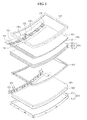
- FIG. 1 is an exploded perspective view that illustrates a display device according to an embodiment of the invention
- FIG. 2 is a cross-sectional view taken along line I-I' of FIG. 1
- FIG. 3 illustrates a rear portion of a lower frame 600 of FIG. 1 .
- a display device includes the lower frame 600, a reflection sheet 900, a light guide plate 300, an optical sheet 201, a light source unit 801, a light source cover 701, an intermediate frame 400, a display panel 100, an upper frame 500, and a light-source driving unit 625.
- a display device may be curved.
- the above-listed elements of the display device may be curved to correspond to a curved shape of the display device.
- the reflection sheet 900, the light guide plate 300, the optical sheet 201, the light source unit 801, the light source cover 701, the intermediate frame 400, and the light-source driving unit 625 are included in a backlight unit.
- the display panel 100 and the backlight unit are assembled into a stacked structure that constitutes a display module.
- the display module may further include the upper frame 500 and the lower frame 600 to protect and fix the display panel 100 and the backlight unit and a driving circuit board that drives the display panel 100.
- the lower frame 600 has an accommodation space therein.
- the reflection sheet 900, the light guide plate 300, the optical sheet 201, the light source unit 801, and the light source cover 701 can be disposed in the accommodation space.
- the lower frame 600 includes a base portion 611 and a plurality of side portions 612.
- the base portion 611 has a rectangular shape, and the side portions 612 protrude from edges of the base portion 611, respectively, to a predetermined height. Edges of the side portions 612 that are adjacent to each other are connected to each other.
- a space surrounded and defined by the side portions 612 and the base portion 611 corresponds to the aforementioned accommodation space.
- a locking projection 635 is formed on an exterior side of at least one of the side portions 612, and the intermediate frame 400 can be fixed to the lower frame 600 by the locking projection 635.
- a portion of one of the side portions 612 is bent to protrude toward the intermediate frame 400, thus forming the locking projection 635.
- the light source unit 801 can emit light.
- the light emitted by the light source unit 801 is transmitted to the display panel 100 through the light guide plate 300 and the optical sheet 201.
- the light source unit 801 includes a light-source circuit board 811 and at least one light source 821.
- a surface of the light-source circuit board 811 is divided into at least one mounting area and a wiring area. If two or more light sources 821 are provided, the light sources 821 are disposed on each corresponding mounting areas, respectively, and a plurality of wirings for transmitting a light-source driving voltage to the light sources 821 are provided in the wiring area.
- the aforementioned light-source driving voltage is generated by the light-source driving unit 625, and then transmitted to the plurality of wirings through a separate connector.
- the light source 821 is a light emission package that includes at least one light emitting diode ("LED").
- a light emission package includes therein a red LED that emits red light, a green LED that emits green light, and a blue LED that emits blue light.
- the light emission package combines the three colors to generate white light.
- the light emission package includes only a blue LED of the aforementioned three LEDs therein, and in such an exemplary embodiment, a phosphor that converts blue light into white light is formed inside a light emission unit of the blue LED. Light emitted from the light source 821 propagates to the light guide plate 300.
- the light guide plate 300 can guide light received from the light source unit 801 to the display panel 100.
- the light guide plate 300 as illustrated in FIGS. 1 and 2 , has a curved polyhedral shape.
- One surface of the light guide plate 300 faces the light source 821 and is defined as a light incident surface 123.
- the light incident surface 123 has a rounded curved shape that is concave downward toward the accommodation space of the lower frame 600.
- Light emitted from the light source 821 is incident to the light incident surface 123, and propagates toward the inside of the light guide plate 300.
- the light guide plate 300 totally reflects the light incident thereinside toward a display area of the display panel 100.
- a plurality of scattering patterns can be further disposed on a lower exterior surface of the light guide plate 300 to improve the reflectivity of the light guide plate 300.
- the light guide plate 300 includes or is formed of a light transmissive material, including acrylic resins such as polymethyl methacrylate (PMMA) and polycarbonate (PC), to efficiently guide light.
- a light transmissive material including acrylic resins such as polymethyl methacrylate (PMMA) and polycarbonate (PC), to efficiently guide light.
- the reflection sheet 900 is disposed between the light guide plate 300 and the lower frame 600.
- the reflection sheet 900 re-reflects light that has propagated through the lower exterior surface of the light guide plate 300 back toward the light guide plate 300, thereby minimizing light attenuation.
- the optical sheet 201 can diffuse and collimate light received from the light guide plate 300.
- the optical sheet 201 is disposed between the light guide plate 300 and the display panel 100.
- the optical sheet 201 includes a diffusion sheet 201a, a light collimation sheet 201b, and a passivation sheet 201 c.
- the diffusion sheet 201 a, the light collimation sheet 201b, and the passivation sheet 201c are sequentially stacked on the light guide plate 300 in the order listed.
- the diffusion sheet 201a diffuses light received from the light guide plate 300 to prevent concentration of the light.
- the light collimation sheet 201b is disposed on the diffusion sheet 201a, and collimates light received from the diffusion sheet 201a toward a direction perpendicular to the display panel 100.
- prisms having a triangular cross-section are arranged in a predetermined arrangement on one surface of the light collimation sheet 201b.
- the passivation sheet 201c is disposed on the collimation sheet 201b, and protects a surface of the light collimation sheet 201b and diffuses light to achieve a more uniform light distribution.
- the light transmitted through the passivation sheet 201c is directed toward the display panel 100.
- the light source cover 701 surrounds a side of the light guide plate 300 to accommodate the light source unit 801 and the light incident surface 123 of the light guide plate 300 within the accommodation space therein.
- the light source cover 701 aligns the light sources 821 on the light incident surface 123 so that the light emitted from the light sources 821 is accurately irradiated to the light incident surface 123 of the light guide plate 300.
- the light source cover 701 may include or be formed of a metal, such as stainless steel.
- the light source cover 701 includes a light-source embedding portion 777a, an upper cover 777b, and a lower cover 777c.
- the light-source embedding portion 777a faces the light source unit 801.
- the upper cover 777b extends from an edge of the light-source embedding portion 777a along an upper exterior surface of the light guide plate 300.
- the lower cover 777c extends from another edge of the light-source embedding portion 777a toward the lower exterior surface of the light guide plate 300.
- the lower cover 777c may have any suitable shape based on a shape of the base portion 611 of the lower frame 600. In an exemplary embodiment, as illustrated in FIG.
- the lower cover 777c may include a first horizontal portion 780a extending from the side of the light-source embedding portion 777a for a predetermined distance, a second horizontal portion 780b disposed more adjacent to the lower surface of the light guide plate 300 than is the first horizontal portion 780a, and an inclined portion 780c connecting the first horizontal portion 780a and the second horizontal portion 780b.
- the light source 821 and the light-source circuit board 811 are disposed in a space surrounded by the light-source embedding portion 777a, the upper cover 777b, and the lower cover 777c.
- a heat dissipation plate 841 is disposed between the light-source circuit board 811 and the light-source embedding portion 777a. Heat generated from the light source 821 can be dissipated externally through the heat dissipation plate 841.
- the intermediate frame 400 is disposed between the light guide plate 300 and the optical sheet 201.
- the intermediate frame 400 supports the display panel 100 and the upper frame 500 while being fixed to the lower frame 600, and maintains a uniform gap between the display panel 100 and the optical sheet 201.
- the intermediate frame 400 may have a rectangular frame shape that includes a first supporting portion 411a, a second supporting portion 411b, and a fixing portion 411c.
- the first supporting portion 411 a is disposed over the plurality of side portions 612 to support the upper frame 500, which covers the first supporting portion 411a from thereabove.
- the second supporting portion 411b extends from an interior side of the first supporting portion 411a toward the optical sheet 201.
- the second supporting portion 411b has a height less than a height of the first supporting portion 411 a.
- a height difference between the first supporting portion 411 a and the second supporting portion 411b produces a space between the upper frame 500 and the second supporting portion 411b, and an edge portion of the display panel 100 is disposed in that space.
- the fixing portion 411c extends from a lower surface of the first supporting portion 411 a toward the side portions 612 of the lower frame 600.
- An engagement groove is defined at an interior side surface of the fixing portion 411c facing the locking projection 635. As the locking projection 635 is engaged with the engagement groove, the intermediate frame 400 may be fixed to the lower frame 600.
- the upper frame 500 has a rectangular frame shape having an opening defined in the center portion thereof.
- the upper frame 500 is disposed on the display panel 100.
- a display area A1 of the display panel 100 is exposed through the opening of the upper frame 500.
- the upper frame 500 covers an edge portion of the display panel 100, an upper surface and a side surface of the first supporting portion 411a, and a side surface of the fixing portion 411c.
- the upper frame 500 includes a front cover 533a that covers the edge portion of the display panel 100 and the upper surface of the first supporting portion 411 a, and a side cover 533b that covers the side surface of the first supporting portion 411a and the side surface of the fixing portion 411c.
- a hook 525 may be disposed at an interior side surface of the side cover 533b, and the hook 525 contacts a lower surface of the fixing portion 411c of the intermediate frame 400.
- the upper frame 500 can be fixed to the intermediate frame 400 by the hook 525.
- one of the side covers 533b may have an aperture.
- a printed circuit board (“PCB") 168 to be described below is externally exposed through the aperture of the side cover 533b.
- the display panel 100 can display an image.
- the display panel 100 includes a lower panel 101 and an upper panel 102 that opposes the lower panel 101.
- the lower panel 101 has an area larger than an area of the upper panel 102.
- the lower panel 101 as illustrated in FIG. 2 , is divided into a display area A1 and a non-display area A2, and the display area A1 of the lower panel 101 and the upper panel 102 face each other.
- the display area A1 has an area substantially the same as an area of the upper panel 102, since the width of the portion of the upper panel 102 that is overlapped by the front cover 533a of the upper frame 500, as shown in FIG. 2 , is negligible as compared to an overall size of the upper panel 102.
- a light control layer is disposed between the display area A1 of the lower panel 101 and the upper panel 102, and any suitable element that may control transmittance of light emitted from the backlight unit may be used as the light control layer.
- the light control layer may be one of a liquid crystal layer, an electro-wetting layer, and an electrophoretic layer.
- the lower panel 101 includes a plurality of gate lines, a plurality of data lines, and a lower polarizer.
- the data lines intersect the gate lines.
- the gate lines extend toward the non-display area A2 to be connected to a gate driver 134, and the data lines extend toward the non-display area A2 to be connected to a data driver 136.
- the gate driver 134 is disposed in the non-display area A2 of the lower panel 101.
- the gate driver 134 generates gate signals based on a gate control signal received from a timing controller, and sequentially transmits the gate signals to the plurality of gate lines.
- the gate driver 134 may include, for example, a shift register that shifts a gate start pulse based on a gate shift clock to produce gate signals.
- the shift register may include a plurality of driving transistors.
- the data driver 136 includes a plurality of data driving integrated circuits ("ICs") 147.
- the data driving ICs 147 receive a digital image data signal and a data control signal applied thereto from the timing controller.
- the data driving ICs 147 sample the digital image data signals according to the data control signal, latch the sampled image data signals corresponding to one horizontal line every horizontal period, and transmit the latched image data signals to the data lines. That is, the data driving ICs 147 convert the digital image data signals received from the timing controller into analog image signals using a gamma voltage received from a power supply, and transmit the analog image signals to the data lines.
- each data driving IC 147 is mounted on a corresponding carrier 146. Some of the carriers 146 are connected between a first data circuit board 168a and the display panel 100, and some of other carriers 146 are connected between a second data circuit board 168b and the display panel 100.
- the first data circuit board 168a and the second data circuit board 168b are electrically connected to each other by a connecting portion 178.
- the connecting portion 178 may be a flexible printed circuit board (FPCB).
- the aforementioned timing controller and power supply are disposed on one of the first data circuit board 168a and the second data circuit board 168b. If the timing controller and power supply are disposed on the first data circuit board 168a, signals received from the timing controller and power supply are transmitted to the second data circuit board 168b through the connecting portion 178. In an alternative exemplary embodiment, if the timing controller and power supply are disposed on the second data circuit board 168b, signals received from the timing controller and power supply are transmitted to the first data circuit board 168a through the connecting portion 178. In an alternative exemplary embodiment, the timing controller and power supply can be disposed on different data circuit boards, respectively.
- the carrier 146 includes input wirings that transmit various signals received from the timing controller and the power supply to the data driving IC 147 and output wirings that transmit image data signals output from the data driving IC 147 to corresponding data lines.
- at least one carrier 146 further includes auxiliary wirings connected to panel wirings disposed in the lower panel 101 that transmit various signals received from the timing controller and the power supply to the gate driver 134.
- the panel wirings connect the auxiliary wirings and the gate driver 134 to each other.
- the panel wirings may be formed on the lower panel 101 in a line-on-glass manner.
- the upper panel 102 includes a common electrode, a shielding layer, and an upper polarizer.
- a transmission axis of the upper polarizer is perpendicular to a transmission axis of the lower polarizer.
- the light-source driving unit 625 is disposed on a rear surface of the lower frame 600.
- the light-source driving unit 625 generates a light source driving voltage used for operation of the light sources 821.
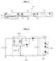
- FIG. 4 illustrates an equivalent circuit of the light sources 821 of the light source unit 801 of FIG. 1 .
- the light sources 821 can be divided into a plurality of light source strings, and in an embodiment, as illustrated in FIG. 4 , the light sources 821 are divided into first, second, and third light source strings 851, 852, and 853.
- the first, second, and third light source strings 851, 852, and 853 are connected to high-voltage lines 881 and 882 in common, and connected to low-voltage lines individually.
- the first, second, and third light source strings 851, 852, and 853 are connected to the high-voltage lines 881 and 882 in common, and the first, second, and third light source strings 851, 852, and 853 are connected to the first, second, and third low-voltage lines 871, 872, and 873, respectively.
- two high-voltage lines 881 and 882 are provided so that the high-voltage lines 881 and 882 do not intersect the first, second, and third low-voltage lines 871, 872, and 873. However, the two high-voltage lines 881 and 882 have an equal electric potential. In an embodiment, a same light-source driving voltage is applied to the high-voltage lines 881 and 882.
- the number of light source strings increases, the number of light sources that can be disposed in each light source string relatively decreases, thus requiring a relatively lower light-source driving voltage, but the number of low-voltage lines increases, which can increase a width W of the light-source circuit board 811.
- the number of light source strings decreases, the number of light sources that can be disposed in each light source string relatively increases, thus requiring a relatively higher light-source driving voltage, but the number of low-voltage lines decreases, which decreases the width W of the light-source circuit board 811.
- the width W of the light-source circuit board 811 affects a size of the backlight unit.
- FIG. 5 illustrates a configuration of the light-source driving unit 625 of FIG. 1
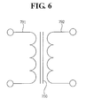
- FIG. 6 is a mimetic view that illustrates a transformer 662 of FIG. 5 .
- the light-source driving unit 625 includes the transformer 662, an output control switching element Tr, a first diode D1, a second diode D2, a first capacitor C1, and a second capacitor C2.
- the transformer 662 increases a level of an input voltage Vin received from the power supply to output the input voltage Vin.
- the output control switching element Tr controls an output from the transformer 662 based on an externally received switching control signal SCS.
- An output level from the transformer 662 varies based on a duty ratio of the switching control signal SCS.
- the first diode D1 and the second diode D2 can prevent a current back flow.
- the first capacitor C1 and the second capacitor C2 can store the output from the transformer 662.
- the voltage stored in the second capacitor C2 is transmitted to the light source 821 as a light-source driving voltage VLED.
- the transformer 662 illustrated in FIG. 5 includes an inductor L, and the inductor L is used to represent an equivalent circuit of the transformer 662.
- An actual transformer 662 does not include the inductor L as illustrated in FIG. 6 . That is, the transformer 662, as illustrated in FIG. 6 , includes a first coil 791, a second coil 792, and a core 750.
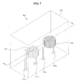
- FIG. 7 illustrates a transformer 662 according to an embodiment of the invention
- FIG. 8 is a cross-sectional view taken along line I-I' of FIG. 7
- FIG. 9 is a cross-sectional view of FIG. 8 absent the first coil 791 and the second coil 792.
- the transformer 662 includes the first coil 791, the second coil 792, a core 750, first terminals 711a and 711b, and second terminals 721a and 721b.
- the core 750 includes a first coil portion 951, a second coil portion 952, and a case portion 950.
- the case portion 950 connects the first coil portion 951 and the second coil portion 952.
- the case portion 950 surrounds the first coil portion 951 and the second coil portion 952, and connects the first coil portion 951 and the second coil portion 952.
- the core 750 as illustrated in FIG. 9 , has thereinside a first accommodation space 351 defined by the first coil portion 951 and the case portion 950 and a second accommodation space 352 defined by the second coil portion 952 and the case portion 950.
- the first coil 791 and the second coil 792 are embedded in the core 750.
- the first coil 791 is disposed in the first accommodation space 351 of the core 750
- the second coil 792 is disposed in the second accommodation space 352 of the core 750.
- first coil portion 951 extends in a direction perpendicular to the lower surface of the case portion 950.
- second coil portion 952 extends in a direction perpendicular to the lower surface of the case portion 950.
- the first coil portion 951 is parallel to the second coil portion 952.
- a portion of the first coil 791, a portion of the case portion 950, and a portion of the second coil 792 are disposed between the first coil portion 951 and the second coil portion 952.
- the core 750 includes or is formed of metal.
- the metal may include a plurality of metal powders.
- at least one metal power includes metal particles and an insulator, and the insulator surrounds the metal particles.
- the metal power does not include the insulator.
- the metal forming the core 750 may include at least one selected from iron, cobalt, and nickel.
- the metal particles forming the core 750 may include at least one selected from iron, cobalt, and nickel.
- a metal such as iron, cobalt, and nickel has a higher permeability than that of ferrite. Accordingly, the transformer 662, including the core 750 that includes iron, can generate a higher voltage than a conventional transformer that includes a ferrite core. Accordingly, if the transformer 662 that includes the iron-containing core 750 is used in the backlight unit of the display device, the number of the aforementioned light source strings can be reduced, which means that a width W of the light-source circuit board 811 can be reduced. As such, the transformer 662 that includes the iron-containing core 750 can enable a backlight unit and a display device including the backlight unit to have a slimmer structure.
- the first coil 791 is rolled around the core 750. In an embodiment, the first coil 791 is rolled around the first coil portion 951 of the core 750. In such an exemplary embodiment, the first coil 791 is disposed in the aforementioned first accommodation space 351. End portions of the first coil 791 are exposed external to the core 750. One end portion of the first coil 791 is connected to one of the first terminals, for example, a first terminal 711 a, and the other end portion of the first coil 791 is connected to another of the first terminals, for example, a first terminal 711b.
- the second coil 792 is rolled around the core 750.
- the second coil 792 is rolled around the second coil portion 952 of the core 750.
- the second coil 792 is disposed in the aforementioned second accommodation space 352. End portions of the second coil 792 are exposed external to the core 750.
- One end portion of the second coil 792 is connected to one of the second terminals, for example, a second terminal 721 a, and the other end portion of the second coil 792 is connected to another of the second terminals, for example, a second terminal 721b.
- the first coil 791 may have a diameter different from that of the second coil 792.
- a coil with a smaller diameter is rolled around the core 750 more times than a coil with a larger diameter.
- the first coil 791 is rolled around the first coil portion 951 of the core 750 four times and the second coil 792 is rolled around the second coil portion 952 of the core 750 eight times, and the second coil 792 has a diameter d2 that is less than a diameter d1 of the first coil 791 (d2 ⁇ d1). Accordingly, since a coil diameter decreases in proportion to the number of times the around which the coil is rolled, a size increase of the transformer 662 can be significantly mitigated, even though the number of times the coil is rolled increases.
- an output voltage induced by the input voltage Vin is applied to the second coil 792.
- the transformer 662 illustrated in FIG. 8 can function as a step-up transformer that can boost the input voltage Vin.
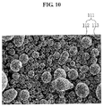
- FIG. 10 illustrates an interior structure of the core 750 of FIG. 8 observed by scanning electron microscopy (SEM).
- the core 750 includes a plurality of metal powders 111, and at least one metal powder 111 includes a metal particle 112 and an insulator 113 surrounding the metal particle 112.
- the transformer 662 illustrated in FIG. 8 can be manufactured in the following manner.
- the first coil 791 and the second coil 792 are disposed in a mold.
- the metal powders 111 are filled in the mold in which the first coil 791 and the second coil 792 are disposed.
- the metal powder 111 includes the metal particles 112 that include the aforementioned iron and the insulator 113 surrounding the metal particles 112.
- the metal powders 111 combine with each other to coagulate.
- the coagulated metal powders 111 form the core 750, including the first coil portion 951, the second coil portion 952, and the case portion 950.
- the core 750 surrounds a portion of the first coil 791 and the second coil 792 aside from the end portions of the first coil 791 and the end portions of the second coil 792.
- the first coil 791 and the second coil 792 are rolled around the first coil portion 951 of the core 750 and the second coil portion 952 of the core 750, respectively.
- the core 750 including the metal powders 111, surrounds the entire first coil 791 and second coil 792. Accordingly, a coupling force between the first and second coils 791 and 792 and the core 750 increases, and an additional supporting member for supporting the first and second coils 791 and 792 and the core 750 is unnecessary.
- FIG. 11 illustrates a transformer 662 according to another embodiment of the invention.
- the transformer 662 of FIG. 11 includes a first coil 791, a second coil 792, a core 750, first terminals 711a and 711b, and second terminals 721a and 721b.
- the first coil 791, the second coil 792, the core 750, the first terminals 711a and 711b, and the second terminals 721a and 721b of the transformer 662 illustrated in FIG. 11 are the same as the first coil 791, the second coil 792, the core 750, the first terminals 711a and 711b, and the second terminals 721a and 721b of the transformer 662 illustrated in FIG. 8 , and thus descriptions pertaining thereto will make reference to FIG. 8 and related descriptions.
- the transformer 662 of FIG. 11 has the following difference compared to the transformer 662 of FIG 8 .
- a first coil portion 951 of FIG. 11 extends parallel to the lower surface of the case portion 950.
- a second coil portion 952 of FIG. 11 extends parallel to the lower surface of the case portion 950.
- a portion of the case portion 950 is disposed between the first coil portion 951 and the second coil portion 952.
- the first coil 791 of the transformer 662 illustrated in FIG. 11 is rolled around the core 750 a greater number of times than the second coil 792 is rolled therearound. Accordingly, the transformer 662 of FIG. 11 functions as a step-down transformer that can decrease the input voltage Vin to a voltage less than that of the input voltage Vin.
- the first coil 791 which is rolled around the core 750 a greater number of times than the second coil 792, has a diameter less than a diameter of the second coil 792.
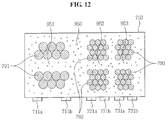
- FIG. 12 is a cross-sectional view that illustrates a transformer 662 according to still another embodiment of the invention.
- the transformer 662 of FIG. 12 includes a first coil 791, a second coil 792, a third coil 793, a core 750, first terminals 711a and 711b, second terminals 721a and 721b, and third terminals 731a and 731b.
- the core 750 includes a first coil portion 951, a second coil portion 952, a third coil portion 953, and a case portion 950.
- the case portion 950 connects the first coil portion 951, the second coil portion 952, and the third coil portion 953.
- the case portion 950 surrounds the first coil portion 951, the second coil portion 952, and the third coil portion 953, and connects the first coil portion 951, the second coil portion 952, and the third coil portion 953.
- the core 750 has thereinside a first accommodation space defined by the first coil portion 951 and the case portion 950, a second accommodation space defined by the second coil portion 952 and the case portion 950, and a third accommodation space defined by the third coil portion 953 and the case portion 950.
- the first coil portion 951 extends parallel to the lower surface of the case portion 950.
- the second coil portion 952 extends parallel to the aforementioned lower surface of the case portion 950.
- the third coil portion 953 extends parallel to the aforementioned lower surface of the case portion 950.
- a portion of the case portion 950 is disposed between the first coil portion 951 and the second coil portion 952. Another portion of the case portion 950 is disposed between the second coil portion 952 and the third coil portion 953.
- the first coil 791 is disposed in the first accommodation space of the core 750 to be rolled around the first coil portion 951
- the second coil 792 is disposed in the second accommodation space of the core 750 to be rolled around the second coil portion 952
- the third coil 793 is disposed in the third accommodation space of the core 750 to be rolled around the third coil portion 953.
- End portions of the first coil 791 are individually connected to the two first terminals 711a and 711b, respectively, end portions of the second coil 792 are individually connected to the two second terminals 721a and 721b, respectively, and end portions of the third coil 793 are individually connected to the two third terminals 731a and 731b, respectively.
- At least two of the first coil 791, the second coil 792, and the third coil 793 may have diameters different from each other.
- a smaller diameter coil is rolled around the core 750 more times than a larger diameter coil.
- the transformer 662 of FIG. 12 is a multiple output transformer 662 that generates output voltages having different levels from each other through the second coil 792 and the third coil 793, respectively.
- FIG. 13 is a cross-sectional view illustrating a transformer 662 according to yet another embodiment of the invention.
- the transformer 662 of FIG. 13 includes a first coil 791, a second coil 792, a third coil 793, a core 750, first terminals 711a and 711b, second terminals 721a and 721b, and third terminals 731a and 731b.
- the first coil 791, the second coil 792, the third coil 793, the core 750, the first terminals 711a and 711b, the second terminals 721a and 721b, and the third terminals 731a and 731b illustrated in FIG. 13 are the same as the first coil 791, the second coil 792, the third coil 793, the core 750, the first terminals 711a and 711b, the second terminals 721a and 721b, and the third terminals 731a and 731b illustrated in FIG. 12 , and thus descriptions pertaining thereto will make reference to FIG. 12 and the related descriptions.
- the first coil 791 of the transformer 662 illustrated in FIG. 13 is disposed between the second coil 792 and the third coil 793, unlike the transformer 662 of FIG. 12 .
- FIG. 14 is an exploded perspective view illustrating a transformer 662 according to yet another embodiment of the invention.
- the transformer 662 illustrated in FIG. 14 is a planar transformer, and includes a first core 421, a second core 422, first, second, third, and fourth substrates 481, 482, 483, and 484, and first, second, third, and fourth coil patterns 491, 492, 493, and 494.
- the first core 421 includes a case portion 423, a coil portion 421c, a first protrusion portion 421a, and a second protrusion portion 421b.
- the coil portion 421c of the first core 421 is disposed between the first protrusion portion 421a and the second protrusion portion 421b.
- the coil portion 421c, the first protrusion portion 421a, and the second protrusion portion 421b of the first core 421 protrude toward the second core 422.
- the first core 421 may include or be formed of metal.
- the first core 421 includes or is formed of a same material as that forming the aforementioned core 750 of FIG. 8 .
- the second core 422 includes a case portion 424, a coil portion 422c, a first protrusion portion 422a, and a second protrusion portion 422b.
- the coil portion 422c of the second core 422 is disposed between the first protrusion portion 422a and the second protrusion portion 422b.
- the coil portion 422c, the first protrusion portion 422a, and the second protrusion portion 422b of the second core 422 protrude toward the first core 421.
- the second core 422 may include or be formed of a same material as that forming the first core 421.
- the second core 422 includes or is formed of a same material the same as that forming the aforementioned core 750 of FIG. 8 .
- the first core 421 and the second core 422 are unitary, i.e., formed as one unit.
- the first, second, third, and fourth substrates 481, 482, 483, and 484 are disposed between the first core 421 and the second core 422.
- the first, second, third, and fourth substrates 481, 482, 483, and 484 surround one of the coil portion 421c of the first core 421 and the coil portion 422c of the second core 422.
- the first, second, third, and fourth substrates 481, 482, 483, and 484 have respective insertion holes 441, 442, 443, and 444, through which the coil portions 421c and 422c may pass.
- the first core 421 and the second core 422 are connected to each other.
- the coil portion 421c of the first core 421 and the coil portion 422c of the second core 422 pass through the insertion holes 441, 442, 443, and 444 of the first, second, third, and fourth substrates 481, 482, 483, and 484 to be connected to each other.
- the first protrusion portion 421a of the first core 421 is connected to the first protrusion portion 422a of the second core 422, and the second protrusion portion 421b of the first core 421 is connected to the second protrusion portion 422b of the second core 422.
- each of the first, second, third, and fourth substrates 481, 482, 483, and 484 is disposed in an accommodation space defined by the case portion 423, the first protrusion portion 421a, the coil portion 421c, the case portion 424, the first protrusion portion 422a, and the coil portion 422c.
- each of the first, second, third, and fourth substrates 481, 482, 483, and 484 is disposed in an accommodation space defined by the case portion 423, the coil portion 421c, the second protrusion portion 421b, the case portion 424, the coil portion 422c, and the second protrusion portion 422b.
- the first coil pattern 491 is disposed on the first substrate 481.
- the first coil pattern 491 surrounds the insertion hole 441 of the first substrate 481.
- the first coil pattern 491 forms a spiral shape.
- second coil pattern 492 is disposed on the second substrate 482.
- the second coil pattern 492 surrounds the insertion hole 442 of the second substrate 482.
- the second coil pattern 492 forms a spiral shape.
- the third coil pattern 493 is disposed on the third substrate 483.
- the third coil pattern 493 surrounds the insertion hole 443 of the third substrate 483.
- the third coil pattern 493 forms a spiral shape.
- the fourth coil pattern 494 is disposed on the fourth substrate 484.
- the fourth coil pattern 494 surrounds the insertion hole 444 of the fourth substrate 484.
- the fourth coil pattern 494 forms a spiral shape.
- the first coil pattern 491 is connected to the third coil pattern 493 through a via hole 402 of the second substrate 482 and a via hole 403 of the third substrate 483.
- the connected first and third coil patterns 491 and 493 correspond to the first coil 791.
- the second coil pattern 492 is connected to the fourth coil pattern 494 through a via hole 403 of the third substrate 483 and a via hole 404 of the fourth substrate 484.
- the connected second and fourth coil patterns 492 and 494 correspond to the second coil 792.
- a reference numeral 401 illustrated in FIG. 14 refers to a via hole of the first substrate 481.
- At least one coil pattern has a width different from a width of another coil pattern.
- coil patterns surrounding the first core 421 or the second core 422 a greater number of times have a smaller width than coil patterns surrounding the first core 421 or the second core 422 a lesser number of times.
- FIG. 15 is an exploded perspective view that illustrates a transformer 662 according to yet another embodiment of the invention.
- the transformer 662 illustrated in FIG. 15 is a planar transformer, and includes a first core 155, a second core 156, first, second, third, and fourth substrates 481, 482, 483, and 484, and first, second, third, and fourth coil patterns 491, 492, 493, and 494.
- the first, second, third, and fourth substrates 481, 482, 483, and 484, and the first, second, third, and fourth coil patterns 491, 492, 493, and 494 illustrated in FIG. 15 are the same as the first, second, third, and fourth substrates 481, 482, 483, and 484, and the first, second, third, and fourth coil patterns 491, 492, 493, and 494 illustrated in FIG. 14 , and thus descriptions pertaining thereto will make reference to FIG. 14 and the related descriptions.
- the first core 155 and the second core 156of the transformer 622 illustrated in FIG. 15 surround an entire portion of the first, second, third, and fourth substrates 481, 482, 483, and 484.
- Each of the first core 155 and the second core 156 may have an area larger than an area of one of the first, second, third, and fourth substrates 481, 482, 483, and 484.
- the first core 155 includes a case portion 155a, a coil portion 155c, and a protrusion portion 155b.
- the coil portion 155c of the first core 155 is disposed at a center portion of the case portion 155a.
- the protrusion portion 155b of the first core 155 is disposed at an edge portion of the case portion 155a, and surrounds the coil portion 155c.
- the coil portion 155c and the protrusion portion 155b of the first core 155 protrude toward the second core 156.
- the first core 155 includes or is formed of a metal.
- the first core 155 includes or is formed of a same material as that forming the aforementioned core 750 of FIG. 8 .
- the second core 156 includes a case portion 156a, a coil portion 156c, and a protrusion portion 156b.
- the coil portion 156c of the second core 156 is disposed at a center portion of the case portion 156a.
- the protrusion portion 156b of the second core 156 is disposed at an edge portion of the case portion 156a, and surrounds the coil portion 156c.
- the coil portion 156c and the protrusion portion 156b of the second core 156 protrude toward the first core 155.
- the second core 156 includes or is formed of a metal.
- the second core 156 includes or is formed of a same material as that forming the aforementioned core 750 of FIG. 8 .
- the first core 155 and the second core 156 are unitary, i.e., formed as one unit.
- the coil portion 155c of the first core 155 and the coil portion 156c of the second core 156 pass through the insertion holes 441, 442, 443, and 444 of the first, second, third, and fourth substrates 481, 482, 483, and 484 to be connected to each other.
- the protrusion portion 155b of the first core 155 is connected to the protrusion portion 156b of the second core 156.
- the first, second, third, and fourth substrates 481, 482, 483, and 484 are disposed in an accommodation space defined by the first core 155 and the second core 156.
- the transformer 662 of FIG. 14 or the transformer 662 of FIG. 15 can be manufactured in the following manner.
- first, second, third, and fourth substrates 481, 482, 483, and 484 are prepared.
- the first coil pattern 491 of the first substrate 481 and the third coil pattern 493 of the third substrate 483 are connected to each other, and the second coil pattern 492 of the second substrate 482 and the fourth coil pattern 494 of the fourth substrate 484 are connected to each other.
- first, second, third, and fourth substrates 481, 482, 483, and 484 are disposed in a mold.
- metal powders 111 are filled into the mold in which the first, second, third, and fourth substrates 481, 482, 483, and 484 are disposed.
- the metal powder 111 includes metal particles 112 that include the aforementioned iron and an insulator 113 surrounding the metal particles 112, for example.
- the metal powders 111 combine to each other to coagulate.
- the coagulated metal powders 111 form the first core 421 and the second core 422, including the first protrusion portions 421a and 421b, the coil portions 421c and 422c, and the second protrusion portions 421b and 422b.
- the first core 421 and the second core 422 surround a portion of the first, second, third, and fourth substrates 481, 482, 483, and 484 or an entire portion thereof, in the transformer 662 manufactured as described hereinabove. Accordingly, a coupling force between the first, second, third, and fourth substrates 481, 482, 483, and 484 and the core 750 may increase, and thus an additional supporting member for supporting the first, second, third, and fourth substrates 481, 482, 483, and 484 and the core 750 is unnecessary.
- At least one of the transformers 662 illustrated in FIGS. 7 , 11 , 12 , 13 , 14 , and 15 can be applied to a common planar display device along with a curved display device.
- a backlight unit may provide the following effects.
- a transformer of a backlight unit has a core that includes a metal such as iron.
- a transformer can generate a higher level voltage than a transformer with a ferrite core. Accordingly, when a transformer that includes a metal-containing core is utilized in a backlight unit, the number of required light source strings can be decreased, and thereby a width of a light-source circuit board may decrease. As a result, a size of the backlight unit may be reduced.
- the core of a transformer includes metal powders.
- the core surrounds an entire portion of a coil. Accordingly, a coupling force between the coils and the core increases, and thereby an additional supporting member for supporting the coils and the core is unnecessary.
- a coil included in a transformer according to embodiments of the invention has a smaller diameter and can be rolled around the core more times. Accordingly, even though the number of times the coil is rolled around the core increases, a size increase of the transformer can be minimized.
Landscapes
- Engineering & Computer Science (AREA)
- Physics & Mathematics (AREA)
- Power Engineering (AREA)
- General Physics & Mathematics (AREA)
- Optics & Photonics (AREA)
- Theoretical Computer Science (AREA)
- Computer Hardware Design (AREA)
- Microelectronics & Electronic Packaging (AREA)
- Nonlinear Science (AREA)
- Planar Illumination Modules (AREA)
- Mathematical Physics (AREA)
- Chemical & Material Sciences (AREA)
- Crystallography & Structural Chemistry (AREA)
- Devices For Indicating Variable Information By Combining Individual Elements (AREA)
Abstract
Description
- Embodiments of the present invention are directed to a backlight unit with a slim structure.
- A liquid crystal display (LCD) is a type of flat panel display (FPDs) that is currently widely used. An LCD device generally includes two substrates that include field-generating electrodes, such as a pixel electrode and a common electrode, and a liquid crystal layer interposed therebetween. Upon applying voltage to the field-generating electrodes, the LCD device rearranges liquid crystal molecules of the liquid crystal layer to control an amount of light passing therethrough.
- An LCD device includes a backlight unit. A backlight unit can be classified as a direct type, an edge type, and a corner type, based on a position of the light sources.
- Recently, light emitting diodes ("LEDs"), which have low-power consumption and high efficiency, have become more widely used as a light source of the backlight unit.
- A backlight unit may include a light source module that includes a plurality of LEDs mounted on a single printed circuit board ("PCB").
- The LEDs are disposed on a light-source circuit board. A width of the light-source circuit board can affect a size of the backlight unit.
- Embodiments of the present invention set out to provide a backlight unit that includes a light-source circuit board with a reduced width, thus enabling a slimmer structure for a display device.
- According to an embodiment of the present invention, a backlight unit includes a light source; and a light-source driving unit configured to drive the light source and that includes a transformer. The transformer includes a core comprising a plurality of metal powders; and a plurality of coils embedded in the core. At least one coil has a diameter different from a diameter of another coil.
- The at least one metal powder may include metal particles and an insulator surrounding the metal particles.
- The at least one metal powder may include at least one of iron, cobalt, and nickel.
- The core may surround the plurality of coils. The core may include a coil portion around which each of the plurality of coils is rolled and a case portion that surrounds the plurality of coils.
- The coil portion and the case portion may be formed as one unit.
- A plurality of coils with a smaller diameter may be rolled around the core more times than a plurality of coils with a larger diameter.
- According to an embodiment of the present invention, a backlight unit includes a light source; and a light-source driving unit configured to drive the light source and that includes a transformer. The transformer inclues a core comprising a plurality of metal powders; a plurality of substrates, each having an insertion hole into which the core is inserted; and a plurality of coil patterns on respective substrates of the plurality of substrates, each coil pattern surrounding the core. At least one coil pattern has a width different from a width of another coil pattern.
- At least one metal powder may include metal particles and an insulator surrounding the metal particles.
- At least one metal powder may include at least one of iron, cobalt, and nickel.
- The core may surround the plurality of substrates. The core may include a coil portion that is inserted into the insertion holes of the plurality of substrates; and a case portion that surrounds the plurality of substrates.
- The coil portion and the case portion may be formed as one unit.
- A plurality of coil patterns with a smaller diameter may be rolled around the core more times than a plurality of coils with a larger width.
- According to an embodiment of the present invention, a light-source driving unit for driving a light source includes a transformer. The transformer includes a core comprising a plurality of metal powders; and a plurality of coils that surround the core. At least one coil has a characteristic dimension different from a characteristic dimension of another coil, and at least one metal powder comprises at least one of iron, cobalt, and nickel.
- The light-source driving unit may further include a plurality of substrates, each having an insertion hole into which the core is inserted. Each of the plurality of coil patterns is disposed on a respective substrate of the plurality of substrates, and the characteristic dimension of a coil may be a width.
- The core may surround the plurality of coils, and the core may further include a coil portion around which each of the plurality of coils is rolled; and a case portion that surrounds the plurality of coils.
- Each of the plurality of coils may be embedded in the core, and the characteristic dimension of a coil may be a diamater.
- The core may surround the plurality of substrates, and the core may further include a coil portion that is inserted into the insertion holes of the plurality of substrates; and a case portion that surrounds the plurality of substrates.
- At least one metal powder may include metal particles and an insulator surrounding the metal particles, and the metal particles may include at least one of iron, cobalt, and nickel.
- A plurality of coils with a smaller characteristic dimension may be rolled around the core more times than a plurality of coils with a larger characteristic dimension.
- At least some of the above and other features of the invention are set out in the claims.
- In addition to the illustrative aspects, embodiments, and features described above, further aspects, embodiments, and features of the invention will become apparent by reference to the drawings and the following detailed description.
-
-
FIG. 1 is an exploded perspective view that illustrates a display device according to an embodiment of the invention. -
FIG. 2 is a cross-sectional view taken along line I-I' ofFIG. 1 . -
FIG. 3 illustrates a rear portion of a lower frame ofFIG. 1 . -
FIG. 4 illustrates an equivalent light source circuit of a light source unit ofFIG. 1 . -
FIG. 5 illustrates a configuration of a light-source driving unit ofFIG. 1 . -
FIG. 6 is a mimetic view that illustrates a transformer ofFIG. 5 . -
FIG. 7 illustrates a transformer according to an embodiment of the invention. -
FIG. 8 is a cross-sectional view taken along line I-I' ofFIG. 7 . -
FIG. 9 is a cross-sectional view ofFIG. 8 absent a first coil and a second coil. -
FIG. 10 illustrates an interior structure of a core ofFIG. 8 observed by scanning electron microscopy (SEM). -
FIG. 11 illustrates a transformer according to another exemplary embodiment. -
FIG. 12 is a cross-sectional view that illustrates a transformer according to still another embodiment of the invention. -
FIG. 13 is a cross-sectional view that illustrates a transformer according to yet another embodiment of the invention. -
FIG. 14 is an exploded perspective view that illustrates a transformer according to yet another embodiment of the invention. -
FIG. 15 is an exploded perspective view that illustrates a transformer according to yet another embodiment of the invention. - Features of the present invention and methods for achieving them will be made clear from embodiments described below in detail with reference to the accompanying drawings. The present invention may, however, be embodied in many different forms and should not be construed as being limited to the embodiments set forth herein. Well-known constituent elements, operations and techniques may not be described in detail in the embodiments
- In the drawings, thicknesses may be exaggerated to clearly describe a plurality of layers and areas. Like reference numbers may be used to denote like elements throughout the specification. When an element or layer is referred to as being "on", "engaged to", "connected to" or "coupled to" another element or layer, it may be directly on, engaged, connected or coupled to the other element or layer, or intervening elements or layers may be present.
- Throughout the specification, when an element is referred to as being "connected" to another element, the element is "directly connected" to the other element, or "electrically connected" to the other element with one or more intervening elements interposed therebetween.
- Hereinafter, a display device according to an embodiment of the invention will be described in detail with reference to
FIGS. 1 to 15 . -
FIG. 1 is an exploded perspective view that illustrates a display device according to an embodiment of the invention,FIG. 2 is a cross-sectional view taken along line I-I' ofFIG. 1 , andFIG. 3 illustrates a rear portion of alower frame 600 ofFIG. 1 . - A display device according to an embodiment of the invention, as illustrated in
FIGS. 1 ,2 , and3 , includes thelower frame 600, areflection sheet 900, alight guide plate 300, anoptical sheet 201, alight source unit 801, alight source cover 701, anintermediate frame 400, adisplay panel 100, anupper frame 500, and a light-source driving unit 625. - A display device according to an embodiment may be curved. The above-listed elements of the display device may be curved to correspond to a curved shape of the display device.
- According to an embodiment of the invention, the
reflection sheet 900, thelight guide plate 300, theoptical sheet 201, thelight source unit 801, thelight source cover 701, theintermediate frame 400, and the light-source driving unit 625 are included in a backlight unit. In such an embodiment, thedisplay panel 100 and the backlight unit are assembled into a stacked structure that constitutes a display module. The display module may further include theupper frame 500 and thelower frame 600 to protect and fix thedisplay panel 100 and the backlight unit and a driving circuit board that drives thedisplay panel 100. - According to an embodiment of the invention, the
lower frame 600 has an accommodation space therein. Thereflection sheet 900, thelight guide plate 300, theoptical sheet 201, thelight source unit 801, and thelight source cover 701 can be disposed in the accommodation space. To secure the accommodation space, thelower frame 600 includes abase portion 611 and a plurality ofside portions 612. In an embodiment, thebase portion 611 has a rectangular shape, and theside portions 612 protrude from edges of thebase portion 611, respectively, to a predetermined height. Edges of theside portions 612 that are adjacent to each other are connected to each other. A space surrounded and defined by theside portions 612 and thebase portion 611 corresponds to the aforementioned accommodation space. In an embodiment, a lockingprojection 635 is formed on an exterior side of at least one of theside portions 612, and theintermediate frame 400 can be fixed to thelower frame 600 by the lockingprojection 635. In an embodiment, a portion of one of theside portions 612 is bent to protrude toward theintermediate frame 400, thus forming the lockingprojection 635. - According to an embodiment of the invention, the
light source unit 801 can emit light. The light emitted by thelight source unit 801 is transmitted to thedisplay panel 100 through thelight guide plate 300 and theoptical sheet 201. In an exemplary embodiment, thelight source unit 801 includes a light-source circuit board 811 and at least onelight source 821. A surface of the light-source circuit board 811 is divided into at least one mounting area and a wiring area. If two or morelight sources 821 are provided, thelight sources 821 are disposed on each corresponding mounting areas, respectively, and a plurality of wirings for transmitting a light-source driving voltage to thelight sources 821 are provided in the wiring area. The aforementioned light-source driving voltage is generated by the light-source driving unit 625, and then transmitted to the plurality of wirings through a separate connector. - According to an embodiment, the
light source 821 is a light emission package that includes at least one light emitting diode ("LED"). In an exemplary embodiment, a light emission package includes therein a red LED that emits red light, a green LED that emits green light, and a blue LED that emits blue light. The light emission package combines the three colors to generate white light. In an alternative exemplary embodiment, the light emission package includes only a blue LED of the aforementioned three LEDs therein, and in such an exemplary embodiment, a phosphor that converts blue light into white light is formed inside a light emission unit of the blue LED. Light emitted from thelight source 821 propagates to thelight guide plate 300. - According to an embodiment of the invention, the
light guide plate 300 can guide light received from thelight source unit 801 to thedisplay panel 100. Thelight guide plate 300, as illustrated inFIGS. 1 and2 , has a curved polyhedral shape. One surface of thelight guide plate 300 faces thelight source 821 and is defined as alight incident surface 123. Thelight incident surface 123 has a rounded curved shape that is concave downward toward the accommodation space of thelower frame 600. Light emitted from thelight source 821 is incident to thelight incident surface 123, and propagates toward the inside of thelight guide plate 300. Thelight guide plate 300 totally reflects the light incident thereinside toward a display area of thedisplay panel 100. In an exemplary embodiment, a plurality of scattering patterns can be further disposed on a lower exterior surface of thelight guide plate 300 to improve the reflectivity of thelight guide plate 300. - According to an embodiment of the invention, the
light guide plate 300 includes or is formed of a light transmissive material, including acrylic resins such as polymethyl methacrylate (PMMA) and polycarbonate (PC), to efficiently guide light. - According to an embodiment of the invention, the
reflection sheet 900 is disposed between thelight guide plate 300 and thelower frame 600. Thereflection sheet 900 re-reflects light that has propagated through the lower exterior surface of thelight guide plate 300 back toward thelight guide plate 300, thereby minimizing light attenuation. - According to an embodiment of the invention, the
optical sheet 201 can diffuse and collimate light received from thelight guide plate 300. Theoptical sheet 201 is disposed between thelight guide plate 300 and thedisplay panel 100. Theoptical sheet 201 includes adiffusion sheet 201a, alight collimation sheet 201b, and apassivation sheet 201 c. Thediffusion sheet 201 a, thelight collimation sheet 201b, and thepassivation sheet 201c are sequentially stacked on thelight guide plate 300 in the order listed. - According to an embodiment of the invention, the
diffusion sheet 201a diffuses light received from thelight guide plate 300 to prevent concentration of the light. - According to an embodiment of the invention, the
light collimation sheet 201b is disposed on thediffusion sheet 201a, and collimates light received from thediffusion sheet 201a toward a direction perpendicular to thedisplay panel 100. To this end, prisms having a triangular cross-section are arranged in a predetermined arrangement on one surface of thelight collimation sheet 201b. - According to an embodiment of the invention, the
passivation sheet 201c is disposed on thecollimation sheet 201b, and protects a surface of thelight collimation sheet 201b and diffuses light to achieve a more uniform light distribution. The light transmitted through thepassivation sheet 201c is directed toward thedisplay panel 100. - According to an embodiment of the invention, the
light source cover 701 surrounds a side of thelight guide plate 300 to accommodate thelight source unit 801 and thelight incident surface 123 of thelight guide plate 300 within the accommodation space therein. Thelight source cover 701 aligns thelight sources 821 on thelight incident surface 123 so that the light emitted from thelight sources 821 is accurately irradiated to thelight incident surface 123 of thelight guide plate 300. Thelight source cover 701 may include or be formed of a metal, such as stainless steel. - According to an embodiment of the invention, the
light source cover 701 includes a light-source embedding portion 777a, anupper cover 777b, and alower cover 777c. The light-source embedding portion 777a faces thelight source unit 801. Theupper cover 777b extends from an edge of the light-source embedding portion 777a along an upper exterior surface of thelight guide plate 300. Thelower cover 777c extends from another edge of the light-source embedding portion 777a toward the lower exterior surface of thelight guide plate 300. Thelower cover 777c may have any suitable shape based on a shape of thebase portion 611 of thelower frame 600. In an exemplary embodiment, as illustrated inFIG. 2 , thelower cover 777c may include a firsthorizontal portion 780a extending from the side of the light-source embedding portion 777a for a predetermined distance, a secondhorizontal portion 780b disposed more adjacent to the lower surface of thelight guide plate 300 than is the firsthorizontal portion 780a, and aninclined portion 780c connecting the firsthorizontal portion 780a and the secondhorizontal portion 780b. - According to an embodiment of the invention, the
light source 821 and the light-source circuit board 811 are disposed in a space surrounded by the light-source embedding portion 777a, theupper cover 777b, and thelower cover 777c. In such an exemplary embodiment, aheat dissipation plate 841 is disposed between the light-source circuit board 811 and the light-source embedding portion 777a. Heat generated from thelight source 821 can be dissipated externally through theheat dissipation plate 841. - According to an embodiment of the invention, the
intermediate frame 400 is disposed between thelight guide plate 300 and theoptical sheet 201. Theintermediate frame 400 supports thedisplay panel 100 and theupper frame 500 while being fixed to thelower frame 600, and maintains a uniform gap between thedisplay panel 100 and theoptical sheet 201. To this end, theintermediate frame 400 may have a rectangular frame shape that includes a first supportingportion 411a, a second supportingportion 411b, and a fixingportion 411c. - According to an embodiment of the invention, the first supporting
portion 411 a is disposed over the plurality ofside portions 612 to support theupper frame 500, which covers the first supportingportion 411a from thereabove. - According to an embodiment of the invention, the second supporting
portion 411b extends from an interior side of the first supportingportion 411a toward theoptical sheet 201. The second supportingportion 411b has a height less than a height of the first supportingportion 411 a. A height difference between the first supportingportion 411 a and the second supportingportion 411b produces a space between theupper frame 500 and the second supportingportion 411b, and an edge portion of thedisplay panel 100 is disposed in that space. - According to an embodiment of the invention, the fixing
portion 411c extends from a lower surface of the first supportingportion 411 a toward theside portions 612 of thelower frame 600. An engagement groove is defined at an interior side surface of the fixingportion 411c facing the lockingprojection 635. As the lockingprojection 635 is engaged with the engagement groove, theintermediate frame 400 may be fixed to thelower frame 600. - According to an embodiment of the invention, the
upper frame 500 has a rectangular frame shape having an opening defined in the center portion thereof. Theupper frame 500 is disposed on thedisplay panel 100. A display area A1 of thedisplay panel 100 is exposed through the opening of theupper frame 500. Theupper frame 500 covers an edge portion of thedisplay panel 100, an upper surface and a side surface of the first supportingportion 411a, and a side surface of the fixingportion 411c. To this end, theupper frame 500 includes afront cover 533a that covers the edge portion of thedisplay panel 100 and the upper surface of the first supportingportion 411 a, and aside cover 533b that covers the side surface of the first supportingportion 411a and the side surface of the fixingportion 411c. - In an embodiment of the invention, a
hook 525 may be disposed at an interior side surface of theside cover 533b, and thehook 525 contacts a lower surface of the fixingportion 411c of theintermediate frame 400. Theupper frame 500 can be fixed to theintermediate frame 400 by thehook 525. In addition, one of the side covers 533b may have an aperture. A printed circuit board ("PCB") 168 to be described below is externally exposed through the aperture of theside cover 533b. - According to an embodiment of the invention, the
display panel 100 can display an image. Thedisplay panel 100 includes alower panel 101 and anupper panel 102 that opposes thelower panel 101. - According to an embodiment of the invention, the
lower panel 101 has an area larger than an area of theupper panel 102. Thelower panel 101, as illustrated inFIG. 2 , is divided into a display area A1 and a non-display area A2, and the display area A1 of thelower panel 101 and theupper panel 102 face each other. The display area A1 has an area substantially the same as an area of theupper panel 102, since the width of the portion of theupper panel 102 that is overlapped by thefront cover 533a of theupper frame 500, as shown inFIG. 2 , is negligible as compared to an overall size of theupper panel 102. - According to an embodiment of the invention, a light control layer is disposed between the display area A1 of the
lower panel 101 and theupper panel 102, and any suitable element that may control transmittance of light emitted from the backlight unit may be used as the light control layer. In an exemplary embodiment, the light control layer may be one of a liquid crystal layer, an electro-wetting layer, and an electrophoretic layer. - According to an embodiment of the invention, the
lower panel 101 includes a plurality of gate lines, a plurality of data lines, and a lower polarizer. The data lines intersect the gate lines. The gate lines extend toward the non-display area A2 to be connected to agate driver 134, and the data lines extend toward the non-display area A2 to be connected to adata driver 136. - According to an embodiment of the invention, the
gate driver 134 is disposed in the non-display area A2 of thelower panel 101. Thegate driver 134 generates gate signals based on a gate control signal received from a timing controller, and sequentially transmits the gate signals to the plurality of gate lines. Thegate driver 134 may include, for example, a shift register that shifts a gate start pulse based on a gate shift clock to produce gate signals. The shift register may include a plurality of driving transistors. - The
data driver 136 includes a plurality of data driving integrated circuits ("ICs") 147. Thedata driving ICs 147 receive a digital image data signal and a data control signal applied thereto from the timing controller. Thedata driving ICs 147 sample the digital image data signals according to the data control signal, latch the sampled image data signals corresponding to one horizontal line every horizontal period, and transmit the latched image data signals to the data lines. That is, thedata driving ICs 147 convert the digital image data signals received from the timing controller into analog image signals using a gamma voltage received from a power supply, and transmit the analog image signals to the data lines. - According to an embodiment of the invention, each
data driving IC 147 is mounted on acorresponding carrier 146. Some of thecarriers 146 are connected between a firstdata circuit board 168a and thedisplay panel 100, and some ofother carriers 146 are connected between a seconddata circuit board 168b and thedisplay panel 100. - The first
data circuit board 168a and the seconddata circuit board 168b are electrically connected to each other by a connectingportion 178. The connectingportion 178 may be a flexible printed circuit board (FPCB). - According to an embodiment of the invention, the aforementioned timing controller and power supply are disposed on one of the first
data circuit board 168a and the seconddata circuit board 168b. If the timing controller and power supply are disposed on the firstdata circuit board 168a, signals received from the timing controller and power supply are transmitted to the seconddata circuit board 168b through the connectingportion 178. In an alternative exemplary embodiment, if the timing controller and power supply are disposed on the seconddata circuit board 168b, signals received from the timing controller and power supply are transmitted to the firstdata circuit board 168a through the connectingportion 178. In an alternative exemplary embodiment, the timing controller and power supply can be disposed on different data circuit boards, respectively. - According to an embodiment of the invention, the
carrier 146 includes input wirings that transmit various signals received from the timing controller and the power supply to thedata driving IC 147 and output wirings that transmit image data signals output from thedata driving IC 147 to corresponding data lines. In an exemplary embodiment, at least onecarrier 146 further includes auxiliary wirings connected to panel wirings disposed in thelower panel 101 that transmit various signals received from the timing controller and the power supply to thegate driver 134. The panel wirings connect the auxiliary wirings and thegate driver 134 to each other. The panel wirings may be formed on thelower panel 101 in a line-on-glass manner. - According to an embodiment of the invention, the
upper panel 102 includes a common electrode, a shielding layer, and an upper polarizer. A transmission axis of the upper polarizer is perpendicular to a transmission axis of the lower polarizer. - According to an embodiment of the invention, the light-
source driving unit 625, as illustrated inFIG. 3 , is disposed on a rear surface of thelower frame 600. The light-source driving unit 625 generates a light source driving voltage used for operation of thelight sources 821. -
FIG. 4 illustrates an equivalent circuit of thelight sources 821 of thelight source unit 801 ofFIG. 1 . - According to an embodiment of the invention, the
light sources 821 can be divided into a plurality of light source strings, and in an embodiment, as illustrated inFIG. 4 , thelight sources 821 are divided into first, second, and third light source strings 851, 852, and 853. The first, second, and third light source strings 851, 852, and 853 are connected to high-voltage lines voltage lines voltage lines FIG. 4 , two high-voltage lines voltage lines voltage lines voltage lines voltage lines - According to an embodiment of the invention, if the number of light source strings increases, the number of light sources that can be disposed in each light source string relatively decreases, thus requiring a relatively lower light-source driving voltage, but the number of low-voltage lines increases, which can increase a width W of the light-
source circuit board 811. In an alternative embodiment of the invention, if the number of light source strings decreases, the number of light sources that can be disposed in each light source string relatively increases, thus requiring a relatively higher light-source driving voltage, but the number of low-voltage lines decreases, which decreases the width W of the light-source circuit board 811. The width W of the light-source circuit board 811 affects a size of the backlight unit. -
FIG. 5 illustrates a configuration of the light-source driving unit 625 ofFIG. 1 , andFIG. 6 is a mimetic view that illustrates atransformer 662 ofFIG. 5 . - According to an embodiment of the invention, the light-
source driving unit 625, as illustrated inFIG. 5 , includes thetransformer 662, an output control switching element Tr, a first diode D1, a second diode D2, a first capacitor C1, and a second capacitor C2. - According to an embodiment of the invention, the
transformer 662 increases a level of an input voltage Vin received from the power supply to output the input voltage Vin. - The output control switching element Tr controls an output from the
transformer 662 based on an externally received switching control signal SCS. An output level from thetransformer 662 varies based on a duty ratio of the switching control signal SCS. - The first diode D1 and the second diode D2 can prevent a current back flow.
- The first capacitor C1 and the second capacitor C2 can store the output from the
transformer 662. The voltage stored in the second capacitor C2 is transmitted to thelight source 821 as a light-source driving voltage VLED. - In an embodiment of the invention, the
transformer 662 illustrated inFIG. 5 includes an inductor L, and the inductor L is used to represent an equivalent circuit of thetransformer 662. Anactual transformer 662 does not include the inductor L as illustrated inFIG. 6 . That is, thetransformer 662, as illustrated inFIG. 6 , includes afirst coil 791, asecond coil 792, and acore 750. -
FIG. 7 illustrates atransformer 662 according to an embodiment of the invention,FIG. 8 is a cross-sectional view taken along line I-I' ofFIG. 7 , andFIG. 9 is a cross-sectional view ofFIG. 8 absent thefirst coil 791 and thesecond coil 792. - According to an embodiment of the invention, the
transformer 662, as illustrated inFIGS. 7 and8 , includes thefirst coil 791, thesecond coil 792, acore 750,first terminals second terminals - According to an embodiment of the invention, the
core 750, as illustrated inFIG. 8 , includes afirst coil portion 951, asecond coil portion 952, and acase portion 950. Thecase portion 950 connects thefirst coil portion 951 and thesecond coil portion 952. In this regard, thecase portion 950 surrounds thefirst coil portion 951 and thesecond coil portion 952, and connects thefirst coil portion 951 and thesecond coil portion 952. In such an embodiment, thecore 750, as illustrated inFIG. 9 , has thereinside afirst accommodation space 351 defined by thefirst coil portion 951 and thecase portion 950 and asecond accommodation space 352 defined by thesecond coil portion 952 and thecase portion 950. - According to an embodiment of the invention, the
first coil 791 and thesecond coil 792 are embedded in thecore 750. In detail, thefirst coil 791 is disposed in thefirst accommodation space 351 of thecore 750, and thesecond coil 792 is disposed in thesecond accommodation space 352 of thecore 750. - Letting a surface of the
case portion 950 contacting thefirst terminals second terminals case portion 950, then thefirst coil portion 951 extends in a direction perpendicular to the lower surface of thecase portion 950. Likewise, thesecond coil portion 952 extends in a direction perpendicular to the lower surface of thecase portion 950. Thefirst coil portion 951 is parallel to thesecond coil portion 952. - According to an embodiment of the invention, a portion of the
first coil 791, a portion of thecase portion 950, and a portion of thesecond coil 792 are disposed between thefirst coil portion 951 and thesecond coil portion 952. - According to an embodiment of the invention, the
core 750 includes or is formed of metal. Herein, the metal may include a plurality of metal powders. In such an exemplary embodiment, at least one metal power includes metal particles and an insulator, and the insulator surrounds the metal particles. In an embodiment, the metal power does not include the insulator. - The metal forming the
core 750 may include at least one selected from iron, cobalt, and nickel. - The metal particles forming the
core 750 may include at least one selected from iron, cobalt, and nickel. - A metal such as iron, cobalt, and nickel has a higher permeability than that of ferrite. Accordingly, the
transformer 662, including thecore 750 that includes iron, can generate a higher voltage than a conventional transformer that includes a ferrite core. Accordingly, if thetransformer 662 that includes the iron-containingcore 750 is used in the backlight unit of the display device, the number of the aforementioned light source strings can be reduced, which means that a width W of the light-source circuit board 811 can be reduced. As such, thetransformer 662 that includes the iron-containingcore 750 can enable a backlight unit and a display device including the backlight unit to have a slimmer structure. - The
first coil 791 is rolled around thecore 750. In an embodiment, thefirst coil 791 is rolled around thefirst coil portion 951 of thecore 750. In such an exemplary embodiment, thefirst coil 791 is disposed in the aforementionedfirst accommodation space 351. End portions of thefirst coil 791 are exposed external to thecore 750. One end portion of thefirst coil 791 is connected to one of the first terminals, for example, a first terminal 711 a, and the other end portion of thefirst coil 791 is connected to another of the first terminals, for example, afirst terminal 711b. - The
second coil 792 is rolled around thecore 750. In an embodiment, thesecond coil 792 is rolled around thesecond coil portion 952 of thecore 750. In such an embodiment, thesecond coil 792 is disposed in the aforementionedsecond accommodation space 352. End portions of thesecond coil 792 are exposed external to thecore 750. One end portion of thesecond coil 792 is connected to one of the second terminals, for example, a second terminal 721 a, and the other end portion of thesecond coil 792 is connected to another of the second terminals, for example, asecond terminal 721b. - The
first coil 791 may have a diameter different from that of thesecond coil 792. In an embodiment, a coil with a smaller diameter is rolled around thecore 750 more times than a coil with a larger diameter. In an exemplary embodiment, as illustrated inFIG. 8 , thefirst coil 791 is rolled around thefirst coil portion 951 of the core 750 four times and thesecond coil 792 is rolled around thesecond coil portion 952 of the core 750 eight times, and thesecond coil 792 has a diameter d2 that is less than a diameter d1 of the first coil 791 (d2<d1). Accordingly, since a coil diameter decreases in proportion to the number of times the around which the coil is rolled, a size increase of thetransformer 662 can be significantly mitigated, even though the number of times the coil is rolled increases. - According to an embodiment, if an input voltage Vin is applied to the
first coil 791 of thetransformer 662 illustrated inFIG. 8 , an output voltage induced by the input voltage Vin is applied to thesecond coil 792. As illustrated inFIG. 8 , as thesecond coil 792 is rolled around the core 750 a greater number of times than that of thefirst coil 791, the output voltage is higher than the input voltage Vin. That is, thetransformer 662 illustrated inFIG. 8 can function as a step-up transformer that can boost the input voltage Vin. -
FIG. 10 illustrates an interior structure of thecore 750 ofFIG. 8 observed by scanning electron microscopy (SEM). - As illustrated in
FIG. 10 , thecore 750 includes a plurality ofmetal powders 111, and at least onemetal powder 111 includes ametal particle 112 and aninsulator 113 surrounding themetal particle 112. - According to embodiments of the invention, the
transformer 662 illustrated inFIG. 8 can be manufactured in the following manner. - First, the
first coil 791 and thesecond coil 792 are disposed in a mold. - Subsequently, the metal powders 111 are filled in the mold in which the
first coil 791 and thesecond coil 792 are disposed. In an embodiment, themetal powder 111 includes themetal particles 112 that include the aforementioned iron and theinsulator 113 surrounding themetal particles 112. - Subsequently, pressure and heat are applied to the metal powders 111 in the mold. In such an embodiment, the metal powders 111 combine with each other to coagulate. The coagulated
metal powders 111 form thecore 750, including thefirst coil portion 951, thesecond coil portion 952, and thecase portion 950. Thecore 750 surrounds a portion of thefirst coil 791 and thesecond coil 792 aside from the end portions of thefirst coil 791 and the end portions of thesecond coil 792. In such an exemplary embodiment, thefirst coil 791 and thesecond coil 792 are rolled around thefirst coil portion 951 of thecore 750 and thesecond coil portion 952 of thecore 750, respectively. - According to embodiments, in the
transformer 662 manufactured in such a manner, thecore 750, including the metal powders 111, surrounds the entirefirst coil 791 andsecond coil 792. Accordingly, a coupling force between the first andsecond coils core 750 increases, and an additional supporting member for supporting the first andsecond coils core 750 is unnecessary. -
FIG. 11 illustrates atransformer 662 according to another embodiment of the invention. - The
transformer 662 ofFIG. 11 includes afirst coil 791, asecond coil 792, acore 750,first terminals second terminals - The
first coil 791, thesecond coil 792, thecore 750, thefirst terminals second terminals transformer 662 illustrated inFIG. 11 are the same as thefirst coil 791, thesecond coil 792, thecore 750, thefirst terminals second terminals transformer 662 illustrated inFIG. 8 , and thus descriptions pertaining thereto will make reference toFIG. 8 and related descriptions. - However, the
transformer 662 ofFIG. 11 has the following difference compared to thetransformer 662 ofFIG 8 . - Letting a lower surface of a
case portion 950 be defined as described hereinabove, afirst coil portion 951 ofFIG. 11 extends parallel to the lower surface of thecase portion 950. Asecond coil portion 952 ofFIG. 11 extends parallel to the lower surface of thecase portion 950. - A portion of the
case portion 950 is disposed between thefirst coil portion 951 and thesecond coil portion 952. - The
first coil 791 of thetransformer 662 illustrated inFIG. 11 is rolled around the core 750 a greater number of times than thesecond coil 792 is rolled therearound. Accordingly, thetransformer 662 ofFIG. 11 functions as a step-down transformer that can decrease the input voltage Vin to a voltage less than that of the input voltage Vin. - In
FIG. 11 , thefirst coil 791, which is rolled around the core 750 a greater number of times than thesecond coil 792, has a diameter less than a diameter of thesecond coil 792. -
FIG. 12 is a cross-sectional view that illustrates atransformer 662 according to still another embodiment of the invention. - The
transformer 662 ofFIG. 12 includes afirst coil 791, asecond coil 792, athird coil 793, acore 750,first terminals second terminals third terminals - The
core 750, as illustrated inFIG. 12 , includes afirst coil portion 951, asecond coil portion 952, athird coil portion 953, and acase portion 950. Thecase portion 950 connects thefirst coil portion 951, thesecond coil portion 952, and thethird coil portion 953. In such an embodiment, thecase portion 950 surrounds thefirst coil portion 951, thesecond coil portion 952, and thethird coil portion 953, and connects thefirst coil portion 951, thesecond coil portion 952, and thethird coil portion 953. In such an embodiment, thecore 750 has thereinside a first accommodation space defined by thefirst coil portion 951 and thecase portion 950, a second accommodation space defined by thesecond coil portion 952 and thecase portion 950, and a third accommodation space defined by thethird coil portion 953 and thecase portion 950. - Letting a surface of the
case portion 950 contacting thefirst terminals second terminals third terminals case portion 950, thefirst coil portion 951 extends parallel to the lower surface of thecase portion 950. Thesecond coil portion 952 extends parallel to the aforementioned lower surface of thecase portion 950. Thethird coil portion 953 extends parallel to the aforementioned lower surface of thecase portion 950. - A portion of the
case portion 950 is disposed between thefirst coil portion 951 and thesecond coil portion 952. Another portion of thecase portion 950 is disposed between thesecond coil portion 952 and thethird coil portion 953. - The
first coil 791 is disposed in the first accommodation space of the core 750 to be rolled around thefirst coil portion 951, thesecond coil 792 is disposed in the second accommodation space of the core 750 to be rolled around thesecond coil portion 952, and thethird coil 793 is disposed in the third accommodation space of the core 750 to be rolled around thethird coil portion 953. - End portions of the
first coil 791 are individually connected to the twofirst terminals second coil 792 are individually connected to the twosecond terminals third coil 793 are individually connected to the twothird terminals - At least two of the
first coil 791, thesecond coil 792, and thethird coil 793 may have diameters different from each other. In an embodiment of the invention, as described hereinabove, a smaller diameter coil is rolled around thecore 750 more times than a larger diameter coil. - The
transformer 662 ofFIG. 12 is amultiple output transformer 662 that generates output voltages having different levels from each other through thesecond coil 792 and thethird coil 793, respectively. -
FIG. 13 is a cross-sectional view illustrating atransformer 662 according to yet another embodiment of the invention. - The
transformer 662 ofFIG. 13 includes afirst coil 791, asecond coil 792, athird coil 793, acore 750,first terminals second terminals third terminals - The
first coil 791, thesecond coil 792, thethird coil 793, thecore 750, thefirst terminals second terminals third terminals FIG. 13 are the same as thefirst coil 791, thesecond coil 792, thethird coil 793, thecore 750, thefirst terminals second terminals third terminals FIG. 12 , and thus descriptions pertaining thereto will make reference toFIG. 12 and the related descriptions. - However, the
first coil 791 of thetransformer 662 illustrated inFIG. 13 is disposed between thesecond coil 792 and thethird coil 793, unlike thetransformer 662 ofFIG. 12 . -
FIG. 14 is an exploded perspective view illustrating atransformer 662 according to yet another embodiment of the invention. - The
transformer 662 illustrated inFIG. 14 is a planar transformer, and includes afirst core 421, asecond core 422, first, second, third, andfourth substrates fourth coil patterns - According to an embodiment of the invention, the
first core 421 includes a case portion 423, acoil portion 421c, afirst protrusion portion 421a, and asecond protrusion portion 421b. Thecoil portion 421c of thefirst core 421 is disposed between thefirst protrusion portion 421a and thesecond protrusion portion 421b. Thecoil portion 421c, thefirst protrusion portion 421a, and thesecond protrusion portion 421b of thefirst core 421 protrude toward thesecond core 422. Thefirst core 421 may include or be formed of metal. In an embodiment, thefirst core 421 includes or is formed of a same material as that forming theaforementioned core 750 ofFIG. 8 . - According to an embodiment of the invention, the
second core 422 includes acase portion 424, acoil portion 422c, afirst protrusion portion 422a, and asecond protrusion portion 422b. Thecoil portion 422c of thesecond core 422 is disposed between thefirst protrusion portion 422a and thesecond protrusion portion 422b. Thecoil portion 422c, thefirst protrusion portion 422a, and thesecond protrusion portion 422b of thesecond core 422 protrude toward thefirst core 421. Thesecond core 422 may include or be formed of a same material as that forming thefirst core 421. In an embodiment, thesecond core 422 includes or is formed of a same material the same as that forming theaforementioned core 750 ofFIG. 8 . - According to an embodiment of the invention, the
first core 421 and thesecond core 422 are unitary, i.e., formed as one unit. - According to an embodiment of the invention, the first, second, third, and
fourth substrates first core 421 and thesecond core 422. - According to an embodiment of the invention, the first, second, third, and
fourth substrates coil portion 421c of thefirst core 421 and thecoil portion 422c of thesecond core 422. To this end, the first, second, third, andfourth substrates coil portions fourth substrates first core 421 and thesecond core 422 are connected to each other. In an exemplary embodiment, thecoil portion 421c of thefirst core 421 and thecoil portion 422c of thesecond core 422 pass through the insertion holes 441, 442, 443, and 444 of the first, second, third, andfourth substrates - According to an embodiment of the invention, the
first protrusion portion 421a of thefirst core 421 is connected to thefirst protrusion portion 422a of thesecond core 422, and thesecond protrusion portion 421b of thefirst core 421 is connected to thesecond protrusion portion 422b of thesecond core 422. - According to an embodiment of the invention, a portion of each of the first, second, third, and
fourth substrates first protrusion portion 421a, thecoil portion 421c, thecase portion 424, thefirst protrusion portion 422a, and thecoil portion 422c. - According to an embodiment of the invention, another portion of each of the first, second, third, and
fourth substrates coil portion 421c, thesecond protrusion portion 421b, thecase portion 424, thecoil portion 422c, and thesecond protrusion portion 422b. - According to an embodiment of the invention, the
first coil pattern 491 is disposed on thefirst substrate 481. Thefirst coil pattern 491 surrounds theinsertion hole 441 of thefirst substrate 481. Thefirst coil pattern 491 forms a spiral shape. - According to an embodiment of the invention,
second coil pattern 492 is disposed on thesecond substrate 482. Thesecond coil pattern 492 surrounds theinsertion hole 442 of thesecond substrate 482. Thesecond coil pattern 492 forms a spiral shape. - According to an embodiment of the invention, the
third coil pattern 493 is disposed on thethird substrate 483. Thethird coil pattern 493 surrounds theinsertion hole 443 of thethird substrate 483. Thethird coil pattern 493 forms a spiral shape. - According to an embodiment of the invention, the
fourth coil pattern 494 is disposed on thefourth substrate 484. Thefourth coil pattern 494 surrounds theinsertion hole 444 of thefourth substrate 484. Thefourth coil pattern 494 forms a spiral shape. - According to an embodiment of the invention, the
first coil pattern 491 is connected to thethird coil pattern 493 through a viahole 402 of thesecond substrate 482 and a viahole 403 of thethird substrate 483. The connected first andthird coil patterns first coil 791. - According to an embodiment of the invention, the
second coil pattern 492 is connected to thefourth coil pattern 494 through a viahole 403 of thethird substrate 483 and a viahole 404 of thefourth substrate 484. The connected second andfourth coil patterns second coil 792. - A
reference numeral 401 illustrated inFIG. 14 refers to a via hole of thefirst substrate 481. - According to an embodiment of the invention, at least one coil pattern has a width different from a width of another coil pattern. In an exemplary embodiment, coil patterns surrounding the
first core 421 or thesecond core 422 a greater number of times have a smaller width than coil patterns surrounding thefirst core 421 or thesecond core 422 a lesser number of times. -
FIG. 15 is an exploded perspective view that illustrates atransformer 662 according to yet another embodiment of the invention. - The
transformer 662 illustrated inFIG. 15 is a planar transformer, and includes afirst core 155, asecond core 156, first, second, third, andfourth substrates fourth coil patterns - According to an embodiment of the invention, the first, second, third, and
fourth substrates fourth coil patterns FIG. 15 are the same as the first, second, third, andfourth substrates fourth coil patterns FIG. 14 , and thus descriptions pertaining thereto will make reference toFIG. 14 and the related descriptions. - According to an embodiment of the invention, the
first core 155 and the second core 156of the transformer 622 illustrated inFIG. 15 surround an entire portion of the first, second, third, andfourth substrates first core 155 and thesecond core 156 may have an area larger than an area of one of the first, second, third, andfourth substrates - According to an embodiment of the invention, the
first core 155 includes acase portion 155a, acoil portion 155c, and aprotrusion portion 155b. Thecoil portion 155c of thefirst core 155 is disposed at a center portion of thecase portion 155a. Theprotrusion portion 155b of thefirst core 155 is disposed at an edge portion of thecase portion 155a, and surrounds thecoil portion 155c. Thecoil portion 155c and theprotrusion portion 155b of thefirst core 155 protrude toward thesecond core 156. Thefirst core 155 includes or is formed of a metal. In an embodiment, thefirst core 155 includes or is formed of a same material as that forming theaforementioned core 750 ofFIG. 8 . - According to an embodiment of the invention, the
second core 156 includes acase portion 156a, acoil portion 156c, and a protrusion portion 156b. Thecoil portion 156c of thesecond core 156 is disposed at a center portion of thecase portion 156a. The protrusion portion 156b of thesecond core 156 is disposed at an edge portion of thecase portion 156a, and surrounds thecoil portion 156c. Thecoil portion 156c and the protrusion portion 156b of thesecond core 156 protrude toward thefirst core 155. Thesecond core 156 includes or is formed of a metal. In an embodiment of the invention, thesecond core 156 includes or is formed of a same material as that forming theaforementioned core 750 ofFIG. 8 . - According to an embodiment of the invention, the
first core 155 and thesecond core 156 are unitary, i.e., formed as one unit. - According to an embodiment of the invention, the
coil portion 155c of thefirst core 155 and thecoil portion 156c of thesecond core 156 pass through the insertion holes 441, 442, 443, and 444 of the first, second, third, andfourth substrates - According to an embodiment of the invention, the
protrusion portion 155b of thefirst core 155 is connected to the protrusion portion 156b of thesecond core 156. - According to an embodiment of the invention, the first, second, third, and
fourth substrates first core 155 and thesecond core 156. - According to embodiments of the invention, the
transformer 662 ofFIG. 14 or thetransformer 662 ofFIG. 15 can be manufactured in the following manner. - First, the first, second, third, and
fourth substrates first coil pattern 491 of thefirst substrate 481 and thethird coil pattern 493 of thethird substrate 483 are connected to each other, and thesecond coil pattern 492 of thesecond substrate 482 and thefourth coil pattern 494 of thefourth substrate 484 are connected to each other. - Subsequently, the first, second, third, and
fourth substrates - Subsequently,
metal powders 111 are filled into the mold in which the first, second, third, andfourth substrates metal powder 111 includesmetal particles 112 that include the aforementioned iron and aninsulator 113 surrounding themetal particles 112, for example. - Subsequently, pressure and heat are applied to the metal powders 111 in the mold. In such an exemplary embodiment, the metal powders 111 combine to each other to coagulate. The coagulated
metal powders 111 form thefirst core 421 and thesecond core 422, including thefirst protrusion portions coil portions second protrusion portions - The
first core 421 and thesecond core 422 surround a portion of the first, second, third, andfourth substrates transformer 662 manufactured as described hereinabove. Accordingly, a coupling force between the first, second, third, andfourth substrates core 750 may increase, and thus an additional supporting member for supporting the first, second, third, andfourth substrates core 750 is unnecessary. - In an embodiment of the invention, at least one of the
transformers 662 illustrated inFIGS. 7 ,11 ,12 ,13 ,14 , and15 can be applied to a common planar display device along with a curved display device. - As set forth hereinabove, a backlight unit according to embodiments of the invention may provide the following effects.
- First, a transformer of a backlight unit according to embodiments of the invention has a core that includes a metal such as iron. Such a transformer can generate a higher level voltage than a transformer with a ferrite core. Accordingly, when a transformer that includes a metal-containing core is utilized in a backlight unit, the number of required light source strings can be decreased, and thereby a width of a light-source circuit board may decrease. As a result, a size of the backlight unit may be reduced.
- Second, the core of a transformer according to embodiments of the invention includes metal powders. The core surrounds an entire portion of a coil. Accordingly, a coupling force between the coils and the core increases, and thereby an additional supporting member for supporting the coils and the core is unnecessary.
- Third, a coil included in a transformer according to embodiments of the invention has a smaller diameter and can be rolled around the core more times. Accordingly, even though the number of times the coil is rolled around the core increases, a size increase of the transformer can be minimized.
- From the foregoing, it will be appreciated that various embodiments of the invention have been described herein for purposes of illustration, and that various modifications may be made without departing from the scope of the present teachings. Accordingly, the various embodiments disclosed herein are not intended to be limiting of the true scope of the present invention.
Claims (12)
- A backlight unit comprising:a light source; anda light-source driving unit configured to drive the light source and that includes a transformer,wherein the transformer comprises:a core comprising a plurality of metal powders; anda plurality of coils embedded in the core, whereinat least one coil has a diameter different from a diameter of another coil.
- A backlight unit according to claim 1, wherein at least one metal powder comprises metal particles and an insulator surrounding the metal particles.
- A backlight unit according to claim 1 or 2, wherein at least one metal powder comprises at least one of iron, cobalt, and nickel.
- A backlight unit according to any preceding claim, wherein the core surrounds the plurality of coils, and the core comprises:a coil portion around which each of the plurality of coils is rolled; anda case portion that surrounds the plurality of coils.
- A backlight unit according to claim 4, wherein the coil portion and the case portion are formed as one unit.
- A backlight unit according to any preceding claim, wherein a plurality of coils with a smaller diameter is rolled around the core more times than a plurality of coils with a larger diameter.
- A backlight unit comprising:a light source; anda light-source driving unit configured to drive the light source and that includes a transformer,wherein the transformer comprises:a core comprising a plurality of metal powders;a plurality of substrates, each having an insertion hole into which the core is inserted; anda plurality of coil patterns on respective substrates of the plurality of substrates, each coil pattern surrounding the core, whereinat least one coil pattern has a width different from a width of another coil pattern.
- A backlight unit according to claim 7, wherein at least one metal powder comprises metal particles and an insulator surrounding the metal particles.
- A backlight unit according to claim 7 or 8, wherein at least one metal powder comprises at least one of iron, cobalt, and nickel.
- A backlight unit according to claim 8, wherein the core surrounds the plurality of substrates, and the core comprises:a coil portion that is inserted into the insertion holes of the plurality of substrates; anda case portion that surrounds the plurality of substrates.
- A backlight unit according to claim 10, wherein the coil portion and the case portion are formed as one unit.
- A backlight unit according to one of claims 8 to 11, wherein a plurality of coil patterns with a smaller width is rolled around the core more times than a plurality of coils with a larger width.
Applications Claiming Priority (1)
| Application Number | Priority Date | Filing Date | Title |
|---|---|---|---|
| KR1020150162267A KR102522283B1 (en) | 2015-11-19 | 2015-11-19 | Backlight unit |
Publications (2)
| Publication Number | Publication Date |
|---|---|
| EP3171668A1 true EP3171668A1 (en) | 2017-05-24 |
| EP3171668B1 EP3171668B1 (en) | 2018-10-31 |
Family
ID=56855324
Family Applications (1)
| Application Number | Title | Priority Date | Filing Date |
|---|---|---|---|
| EP16186891.4A Not-in-force EP3171668B1 (en) | 2015-11-19 | 2016-09-01 | Backlight unit |
Country Status (4)
| Country | Link |
|---|---|
| US (1) | US9826580B2 (en) |
| EP (1) | EP3171668B1 (en) |
| KR (1) | KR102522283B1 (en) |
| CN (1) | CN106952619A (en) |
Cited By (1)
| Publication number | Priority date | Publication date | Assignee | Title |
|---|---|---|---|---|
| FR3077398A1 (en) * | 2018-01-29 | 2019-08-02 | Novares France | DISPLAY DEVICE AND METHOD FOR MANUFACTURING THE SAME |
Citations (1)
| Publication number | Priority date | Publication date | Assignee | Title |
|---|---|---|---|---|
| US20090108979A1 (en) * | 2007-10-25 | 2009-04-30 | Taiyo Yuden Co., Ltd. | Transformer for power supply |
Family Cites Families (17)
| Publication number | Priority date | Publication date | Assignee | Title |
|---|---|---|---|---|
| US4601765A (en) * | 1983-05-05 | 1986-07-22 | General Electric Company | Powdered iron core magnetic devices |
| GB8625329D0 (en) * | 1986-10-22 | 1986-11-26 | Valor Int Ltd | Control gear for gas discharge lighting |
| JPH05304035A (en) | 1992-04-25 | 1993-11-16 | Murata Mfg Co Ltd | Chip type common mode choke coil and manufacturing method thereof |
| JP4684461B2 (en) * | 2000-04-28 | 2011-05-18 | パナソニック株式会社 | Method for manufacturing magnetic element |
| JP4168145B2 (en) * | 2001-06-14 | 2008-10-22 | ボビナドス デ トランスフォルマドーレス エセ.エレ. | Power supply device and liquid crystal display unit having such power supply device |
| US7088334B2 (en) * | 2001-06-28 | 2006-08-08 | Matsushita Electric Industrial Co., Ltd. | Liquid crystal display device and manufacturing method thereof, and drive control method of lighting unit |
| JP4711593B2 (en) | 2002-06-07 | 2011-06-29 | Jfeスチール株式会社 | Planar magnetic element |
| KR200385970Y1 (en) * | 2002-10-02 | 2005-06-07 | 다폰 일렉트로닉스 코퍼레이션 | multi-lamp backlight system |
| US20050007232A1 (en) | 2003-06-12 | 2005-01-13 | Nec Tokin Corporation | Magnetic core and coil component using the same |
| KR100661356B1 (en) * | 2005-08-10 | 2006-12-27 | 삼성전자주식회사 | Balance Coil and Backlight Drive Inverter |
| US8054001B2 (en) * | 2006-09-18 | 2011-11-08 | O2Micro Inc | Circuit structure for LCD backlight |
| CN101610619B (en) * | 2008-06-20 | 2012-12-05 | 国琏电子(上海)有限公司 | Backlight module |
| CN102117599A (en) * | 2010-01-05 | 2011-07-06 | 台达电子工业股份有限公司 | Backlight driving circuit suitable for liquid crystal display panel |
| KR101187970B1 (en) * | 2010-12-21 | 2012-10-05 | 삼성전기주식회사 | Planar transformer, and driver having thereof and display apparatus |
| JP5855671B2 (en) | 2011-10-14 | 2016-02-09 | 株式会社村田製作所 | Metal powder and electronic parts |
| FR2990556B1 (en) * | 2012-05-09 | 2014-05-30 | Hispano Suiza Sa | THREE-PHASE TRIPHASE ROTATING TRANSFORMER FREE |
| KR101983140B1 (en) | 2013-06-21 | 2019-05-28 | 삼성전기주식회사 | Metal magnetic powder and method for forming the same, and inductor manufactured using the metal magnetic powder |
-
2015
- 2015-11-19 KR KR1020150162267A patent/KR102522283B1/en active Active
-
2016
- 2016-06-29 US US15/197,182 patent/US9826580B2/en not_active Expired - Fee Related
- 2016-09-01 EP EP16186891.4A patent/EP3171668B1/en not_active Not-in-force
- 2016-09-26 CN CN201610851049.7A patent/CN106952619A/en active Pending
Patent Citations (1)
| Publication number | Priority date | Publication date | Assignee | Title |
|---|---|---|---|---|
| US20090108979A1 (en) * | 2007-10-25 | 2009-04-30 | Taiyo Yuden Co., Ltd. | Transformer for power supply |
Cited By (1)
| Publication number | Priority date | Publication date | Assignee | Title |
|---|---|---|---|---|
| FR3077398A1 (en) * | 2018-01-29 | 2019-08-02 | Novares France | DISPLAY DEVICE AND METHOD FOR MANUFACTURING THE SAME |
Also Published As
| Publication number | Publication date |
|---|---|
| CN106952619A (en) | 2017-07-14 |
| US20170150557A1 (en) | 2017-05-25 |
| KR20170059028A (en) | 2017-05-30 |
| US9826580B2 (en) | 2017-11-21 |
| EP3171668B1 (en) | 2018-10-31 |
| KR102522283B1 (en) | 2023-04-19 |
Similar Documents
| Publication | Publication Date | Title |
|---|---|---|
| US7927000B2 (en) | Backlight assembly and cover for a compact display apparatus | |
| CN101118051B (en) | Luminescence unit, the backlight assembly with this luminescence unit and display device | |
| JP5258978B2 (en) | LED substrate, backlight unit, and liquid crystal display device | |
| JP5306481B2 (en) | LED substrate, backlight unit, and liquid crystal display device | |
| CN101819339B (en) | Display device | |
| US10739639B2 (en) | Backlight apparatus | |
| EP1930958A2 (en) | Light emitting diode package, and light source unit and backlight unit including the same | |
| JP2008059786A (en) | Illumination device and display device including the same | |
| JP2008096950A (en) | Backlight assembly and liquid crystal display device including the same | |
| US20100283936A1 (en) | Liquid crystal display device including LED light source | |
| CN109087584B (en) | Display device | |
| CN102314021A (en) | Liquid crystal display | |
| CN101311616A (en) | Light source module, backlight assembly, display device and method thereof | |
| CN106547126B (en) | display screen | |
| US10276113B2 (en) | Display device | |
| CN101416102A (en) | Light-emitting device, illuminating device comprising same, and liquid crystal display | |
| EP3171668B1 (en) | Backlight unit | |
| US8475005B2 (en) | Backlight unit and display device including the same | |
| KR100541533B1 (en) | Backlight for LCD | |
| KR101231333B1 (en) | Transformer and diplay apparatus thereof | |
| KR20140018045A (en) | Liquid crystal display device | |
| CN104603520B (en) | Light irradiation device, backlight device and display device | |
| KR200415351Y1 (en) | Improved Structure of Backlight Module | |
| US20220252777A1 (en) | Linear light-emitting device |
Legal Events
| Date | Code | Title | Description |
|---|---|---|---|
| PUAI | Public reference made under article 153(3) epc to a published international application that has entered the european phase |
Free format text: ORIGINAL CODE: 0009012 |
|
| STAA | Information on the status of an ep patent application or granted ep patent |
Free format text: STATUS: THE APPLICATION HAS BEEN PUBLISHED |
|
| AK | Designated contracting states |
Kind code of ref document: A1 Designated state(s): AL AT BE BG CH CY CZ DE DK EE ES FI FR GB GR HR HU IE IS IT LI LT LU LV MC MK MT NL NO PL PT RO RS SE SI SK SM TR |
|
| AX | Request for extension of the european patent |
Extension state: BA ME |
|
| STAA | Information on the status of an ep patent application or granted ep patent |
Free format text: STATUS: REQUEST FOR EXAMINATION WAS MADE |
|
| 17P | Request for examination filed |
Effective date: 20171124 |
|
| RBV | Designated contracting states (corrected) |
Designated state(s): AL AT BE BG CH CY CZ DE DK EE ES FI FR GB GR HR HU IE IS IT LI LT LU LV MC MK MT NL NO PL PT RO RS SE SI SK SM TR |
|
| REG | Reference to a national code |
Ref country code: DE Ref legal event code: R079 Ref document number: 602016006758 Country of ref document: DE Free format text: PREVIOUS MAIN CLASS: H05B0033080000 Ipc: G02B0006000000 |
|
| GRAP | Despatch of communication of intention to grant a patent |
Free format text: ORIGINAL CODE: EPIDOSNIGR1 |
|
| STAA | Information on the status of an ep patent application or granted ep patent |
Free format text: STATUS: GRANT OF PATENT IS INTENDED |
|
| RIC1 | Information provided on ipc code assigned before grant |
Ipc: F21V 8/00 20060101ALI20180301BHEP Ipc: G02F 1/1335 20060101ALI20180301BHEP Ipc: G09G 3/34 20060101ALI20180301BHEP Ipc: G02B 6/00 20060101AFI20180301BHEP Ipc: G02F 1/13 20060101ALI20180301BHEP Ipc: H01F 27/02 20060101ALI20180301BHEP Ipc: H05B 33/08 20060101ALI20180301BHEP Ipc: H01F 27/28 20060101ALI20180301BHEP |
|
| INTG | Intention to grant announced |
Effective date: 20180315 |
|
| GRAS | Grant fee paid |
Free format text: ORIGINAL CODE: EPIDOSNIGR3 |
|
| GRAA | (expected) grant |
Free format text: ORIGINAL CODE: 0009210 |
|
| STAA | Information on the status of an ep patent application or granted ep patent |
Free format text: STATUS: THE PATENT HAS BEEN GRANTED |
|
| AK | Designated contracting states |
Kind code of ref document: B1 Designated state(s): AL AT BE BG CH CY CZ DE DK EE ES FI FR GB GR HR HU IE IS IT LI LT LU LV MC MK MT NL NO PL PT RO RS SE SI SK SM TR |
|
| REG | Reference to a national code |
Ref country code: CH Ref legal event code: EP Ref country code: GB Ref legal event code: FG4D |
|
| REG | Reference to a national code |
Ref country code: AT Ref legal event code: REF Ref document number: 1060071 Country of ref document: AT Kind code of ref document: T Effective date: 20181115 |
|
| REG | Reference to a national code |
Ref country code: DE Ref legal event code: R096 Ref document number: 602016006758 Country of ref document: DE |
|
| REG | Reference to a national code |
Ref country code: IE Ref legal event code: FG4D |
|
| REG | Reference to a national code |
Ref country code: NL Ref legal event code: MP Effective date: 20181031 |
|
| REG | Reference to a national code |
Ref country code: LT Ref legal event code: MG4D |
|
| REG | Reference to a national code |
Ref country code: AT Ref legal event code: MK05 Ref document number: 1060071 Country of ref document: AT Kind code of ref document: T Effective date: 20181031 |
|
| PG25 | Lapsed in a contracting state [announced via postgrant information from national office to epo] |
Ref country code: ES Free format text: LAPSE BECAUSE OF FAILURE TO SUBMIT A TRANSLATION OF THE DESCRIPTION OR TO PAY THE FEE WITHIN THE PRESCRIBED TIME-LIMIT Effective date: 20181031 Ref country code: LV Free format text: LAPSE BECAUSE OF FAILURE TO SUBMIT A TRANSLATION OF THE DESCRIPTION OR TO PAY THE FEE WITHIN THE PRESCRIBED TIME-LIMIT Effective date: 20181031 Ref country code: IS Free format text: LAPSE BECAUSE OF FAILURE TO SUBMIT A TRANSLATION OF THE DESCRIPTION OR TO PAY THE FEE WITHIN THE PRESCRIBED TIME-LIMIT Effective date: 20190228 Ref country code: AT Free format text: LAPSE BECAUSE OF FAILURE TO SUBMIT A TRANSLATION OF THE DESCRIPTION OR TO PAY THE FEE WITHIN THE PRESCRIBED TIME-LIMIT Effective date: 20181031 Ref country code: PL Free format text: LAPSE BECAUSE OF FAILURE TO SUBMIT A TRANSLATION OF THE DESCRIPTION OR TO PAY THE FEE WITHIN THE PRESCRIBED TIME-LIMIT Effective date: 20181031 Ref country code: NO Free format text: LAPSE BECAUSE OF FAILURE TO SUBMIT A TRANSLATION OF THE DESCRIPTION OR TO PAY THE FEE WITHIN THE PRESCRIBED TIME-LIMIT Effective date: 20190131 Ref country code: LT Free format text: LAPSE BECAUSE OF FAILURE TO SUBMIT A TRANSLATION OF THE DESCRIPTION OR TO PAY THE FEE WITHIN THE PRESCRIBED TIME-LIMIT Effective date: 20181031 Ref country code: FI Free format text: LAPSE BECAUSE OF FAILURE TO SUBMIT A TRANSLATION OF THE DESCRIPTION OR TO PAY THE FEE WITHIN THE PRESCRIBED TIME-LIMIT Effective date: 20181031 Ref country code: BG Free format text: LAPSE BECAUSE OF FAILURE TO SUBMIT A TRANSLATION OF THE DESCRIPTION OR TO PAY THE FEE WITHIN THE PRESCRIBED TIME-LIMIT Effective date: 20190131 Ref country code: HR Free format text: LAPSE BECAUSE OF FAILURE TO SUBMIT A TRANSLATION OF THE DESCRIPTION OR TO PAY THE FEE WITHIN THE PRESCRIBED TIME-LIMIT Effective date: 20181031 |
|
| PG25 | Lapsed in a contracting state [announced via postgrant information from national office to epo] |
Ref country code: RS Free format text: LAPSE BECAUSE OF FAILURE TO SUBMIT A TRANSLATION OF THE DESCRIPTION OR TO PAY THE FEE WITHIN THE PRESCRIBED TIME-LIMIT Effective date: 20181031 Ref country code: GR Free format text: LAPSE BECAUSE OF FAILURE TO SUBMIT A TRANSLATION OF THE DESCRIPTION OR TO PAY THE FEE WITHIN THE PRESCRIBED TIME-LIMIT Effective date: 20190201 Ref country code: PT Free format text: LAPSE BECAUSE OF FAILURE TO SUBMIT A TRANSLATION OF THE DESCRIPTION OR TO PAY THE FEE WITHIN THE PRESCRIBED TIME-LIMIT Effective date: 20190301 Ref country code: SE Free format text: LAPSE BECAUSE OF FAILURE TO SUBMIT A TRANSLATION OF THE DESCRIPTION OR TO PAY THE FEE WITHIN THE PRESCRIBED TIME-LIMIT Effective date: 20181031 Ref country code: AL Free format text: LAPSE BECAUSE OF FAILURE TO SUBMIT A TRANSLATION OF THE DESCRIPTION OR TO PAY THE FEE WITHIN THE PRESCRIBED TIME-LIMIT Effective date: 20181031 Ref country code: NL Free format text: LAPSE BECAUSE OF FAILURE TO SUBMIT A TRANSLATION OF THE DESCRIPTION OR TO PAY THE FEE WITHIN THE PRESCRIBED TIME-LIMIT Effective date: 20181031 |
|
| PG25 | Lapsed in a contracting state [announced via postgrant information from national office to epo] |
Ref country code: DK Free format text: LAPSE BECAUSE OF FAILURE TO SUBMIT A TRANSLATION OF THE DESCRIPTION OR TO PAY THE FEE WITHIN THE PRESCRIBED TIME-LIMIT Effective date: 20181031 Ref country code: IT Free format text: LAPSE BECAUSE OF FAILURE TO SUBMIT A TRANSLATION OF THE DESCRIPTION OR TO PAY THE FEE WITHIN THE PRESCRIBED TIME-LIMIT Effective date: 20181031 Ref country code: CZ Free format text: LAPSE BECAUSE OF FAILURE TO SUBMIT A TRANSLATION OF THE DESCRIPTION OR TO PAY THE FEE WITHIN THE PRESCRIBED TIME-LIMIT Effective date: 20181031 |
|
| REG | Reference to a national code |
Ref country code: DE Ref legal event code: R097 Ref document number: 602016006758 Country of ref document: DE |
|
| PG25 | Lapsed in a contracting state [announced via postgrant information from national office to epo] |
Ref country code: SK Free format text: LAPSE BECAUSE OF FAILURE TO SUBMIT A TRANSLATION OF THE DESCRIPTION OR TO PAY THE FEE WITHIN THE PRESCRIBED TIME-LIMIT Effective date: 20181031 Ref country code: RO Free format text: LAPSE BECAUSE OF FAILURE TO SUBMIT A TRANSLATION OF THE DESCRIPTION OR TO PAY THE FEE WITHIN THE PRESCRIBED TIME-LIMIT Effective date: 20181031 Ref country code: SM Free format text: LAPSE BECAUSE OF FAILURE TO SUBMIT A TRANSLATION OF THE DESCRIPTION OR TO PAY THE FEE WITHIN THE PRESCRIBED TIME-LIMIT Effective date: 20181031 Ref country code: EE Free format text: LAPSE BECAUSE OF FAILURE TO SUBMIT A TRANSLATION OF THE DESCRIPTION OR TO PAY THE FEE WITHIN THE PRESCRIBED TIME-LIMIT Effective date: 20181031 |
|
| PLBE | No opposition filed within time limit |
Free format text: ORIGINAL CODE: 0009261 |
|
| STAA | Information on the status of an ep patent application or granted ep patent |
Free format text: STATUS: NO OPPOSITION FILED WITHIN TIME LIMIT |
|
| 26N | No opposition filed |
Effective date: 20190801 |
|
| PG25 | Lapsed in a contracting state [announced via postgrant information from national office to epo] |
Ref country code: SI Free format text: LAPSE BECAUSE OF FAILURE TO SUBMIT A TRANSLATION OF THE DESCRIPTION OR TO PAY THE FEE WITHIN THE PRESCRIBED TIME-LIMIT Effective date: 20181031 |
|
| PG25 | Lapsed in a contracting state [announced via postgrant information from national office to epo] |
Ref country code: TR Free format text: LAPSE BECAUSE OF FAILURE TO SUBMIT A TRANSLATION OF THE DESCRIPTION OR TO PAY THE FEE WITHIN THE PRESCRIBED TIME-LIMIT Effective date: 20181031 |
|
| PG25 | Lapsed in a contracting state [announced via postgrant information from national office to epo] |
Ref country code: MC Free format text: LAPSE BECAUSE OF FAILURE TO SUBMIT A TRANSLATION OF THE DESCRIPTION OR TO PAY THE FEE WITHIN THE PRESCRIBED TIME-LIMIT Effective date: 20181031 |
|
| REG | Reference to a national code |
Ref country code: CH Ref legal event code: PL |
|
| PG25 | Lapsed in a contracting state [announced via postgrant information from national office to epo] |
Ref country code: LI Free format text: LAPSE BECAUSE OF NON-PAYMENT OF DUE FEES Effective date: 20190930 Ref country code: LU Free format text: LAPSE BECAUSE OF NON-PAYMENT OF DUE FEES Effective date: 20190901 Ref country code: CH Free format text: LAPSE BECAUSE OF NON-PAYMENT OF DUE FEES Effective date: 20190930 Ref country code: IE Free format text: LAPSE BECAUSE OF NON-PAYMENT OF DUE FEES Effective date: 20190901 |
|
| REG | Reference to a national code |
Ref country code: BE Ref legal event code: MM Effective date: 20190930 |
|
| PG25 | Lapsed in a contracting state [announced via postgrant information from national office to epo] |
Ref country code: BE Free format text: LAPSE BECAUSE OF NON-PAYMENT OF DUE FEES Effective date: 20190930 |
|
| PGFP | Annual fee paid to national office [announced via postgrant information from national office to epo] |
Ref country code: GB Payment date: 20200910 Year of fee payment: 5 Ref country code: FR Payment date: 20200910 Year of fee payment: 5 Ref country code: DE Payment date: 20200908 Year of fee payment: 5 |
|
| PG25 | Lapsed in a contracting state [announced via postgrant information from national office to epo] |
Ref country code: CY Free format text: LAPSE BECAUSE OF FAILURE TO SUBMIT A TRANSLATION OF THE DESCRIPTION OR TO PAY THE FEE WITHIN THE PRESCRIBED TIME-LIMIT Effective date: 20181031 |
|
| PG25 | Lapsed in a contracting state [announced via postgrant information from national office to epo] |
Ref country code: HU Free format text: LAPSE BECAUSE OF FAILURE TO SUBMIT A TRANSLATION OF THE DESCRIPTION OR TO PAY THE FEE WITHIN THE PRESCRIBED TIME-LIMIT; INVALID AB INITIO Effective date: 20160901 Ref country code: MT Free format text: LAPSE BECAUSE OF FAILURE TO SUBMIT A TRANSLATION OF THE DESCRIPTION OR TO PAY THE FEE WITHIN THE PRESCRIBED TIME-LIMIT Effective date: 20181031 |
|
| REG | Reference to a national code |
Ref country code: DE Ref legal event code: R119 Ref document number: 602016006758 Country of ref document: DE |
|
| GBPC | Gb: european patent ceased through non-payment of renewal fee |
Effective date: 20210901 |
|
| PG25 | Lapsed in a contracting state [announced via postgrant information from national office to epo] |
Ref country code: MK Free format text: LAPSE BECAUSE OF FAILURE TO SUBMIT A TRANSLATION OF THE DESCRIPTION OR TO PAY THE FEE WITHIN THE PRESCRIBED TIME-LIMIT Effective date: 20181031 |
|
| PG25 | Lapsed in a contracting state [announced via postgrant information from national office to epo] |
Ref country code: GB Free format text: LAPSE BECAUSE OF NON-PAYMENT OF DUE FEES Effective date: 20210901 Ref country code: FR Free format text: LAPSE BECAUSE OF NON-PAYMENT OF DUE FEES Effective date: 20210930 Ref country code: DE Free format text: LAPSE BECAUSE OF NON-PAYMENT OF DUE FEES Effective date: 20220401 |