EP3171514A1 - Differential summing node - Google Patents
Differential summing node Download PDFInfo
- Publication number
- EP3171514A1 EP3171514A1 EP15195360.1A EP15195360A EP3171514A1 EP 3171514 A1 EP3171514 A1 EP 3171514A1 EP 15195360 A EP15195360 A EP 15195360A EP 3171514 A1 EP3171514 A1 EP 3171514A1
- Authority
- EP
- European Patent Office
- Prior art keywords
- differential
- signal
- output
- summing node
- coupled
- Prior art date
- Legal status (The legal status is an assumption and is not a legal conclusion. Google has not performed a legal analysis and makes no representation as to the accuracy of the status listed.)
- Withdrawn
Links
Images



Classifications
-
- H—ELECTRICITY
- H03—ELECTRONIC CIRCUITRY
- H03D—DEMODULATION OR TRANSFERENCE OF MODULATION FROM ONE CARRIER TO ANOTHER
- H03D7/00—Transference of modulation from one carrier to another, e.g. frequency-changing
- H03D7/12—Transference of modulation from one carrier to another, e.g. frequency-changing by means of semiconductor devices having more than two electrodes
-
- H—ELECTRICITY
- H03—ELECTRONIC CIRCUITRY
- H03M—CODING; DECODING; CODE CONVERSION IN GENERAL
- H03M3/00—Conversion of analogue values to or from differential modulation
- H03M3/30—Delta-sigma modulation
- H03M3/322—Continuously compensating for, or preventing, undesired influence of physical parameters
- H03M3/358—Continuously compensating for, or preventing, undesired influence of physical parameters of non-linear distortion, e.g. instability
- H03M3/36—Continuously compensating for, or preventing, undesired influence of physical parameters of non-linear distortion, e.g. instability by temporarily adapting the operation upon detection of instability conditions
- H03M3/362—Continuously compensating for, or preventing, undesired influence of physical parameters of non-linear distortion, e.g. instability by temporarily adapting the operation upon detection of instability conditions in feedback mode, e.g. by reducing the order of the modulator
-
- H—ELECTRICITY
- H03—ELECTRONIC CIRCUITRY
- H03F—AMPLIFIERS
- H03F1/00—Details of amplifiers with only discharge tubes, only semiconductor devices or only unspecified devices as amplifying elements
- H03F1/32—Modifications of amplifiers to reduce non-linear distortion
- H03F1/3211—Modifications of amplifiers to reduce non-linear distortion in differential amplifiers
-
- H—ELECTRICITY
- H03—ELECTRONIC CIRCUITRY
- H03F—AMPLIFIERS
- H03F3/00—Amplifiers with only discharge tubes or only semiconductor devices as amplifying elements
- H03F3/45—Differential amplifiers
- H03F3/45071—Differential amplifiers with semiconductor devices only
- H03F3/45076—Differential amplifiers with semiconductor devices only characterised by the way of implementation of the active amplifying circuit in the differential amplifier
- H03F3/45179—Differential amplifiers with semiconductor devices only characterised by the way of implementation of the active amplifying circuit in the differential amplifier using MOSFET transistors as the active amplifying circuit
- H03F3/45183—Long tailed pairs
-
- H—ELECTRICITY
- H03—ELECTRONIC CIRCUITRY
- H03F—AMPLIFIERS
- H03F3/00—Amplifiers with only discharge tubes or only semiconductor devices as amplifying elements
- H03F3/45—Differential amplifiers
- H03F3/45071—Differential amplifiers with semiconductor devices only
- H03F3/45076—Differential amplifiers with semiconductor devices only characterised by the way of implementation of the active amplifying circuit in the differential amplifier
- H03F3/45475—Differential amplifiers with semiconductor devices only characterised by the way of implementation of the active amplifying circuit in the differential amplifier using IC blocks as the active amplifying circuit
-
- H—ELECTRICITY
- H03—ELECTRONIC CIRCUITRY
- H03M—CODING; DECODING; CODE CONVERSION IN GENERAL
- H03M3/00—Conversion of analogue values to or from differential modulation
- H03M3/30—Delta-sigma modulation
- H03M3/39—Structural details of delta-sigma modulators, e.g. incremental delta-sigma modulators
- H03M3/412—Structural details of delta-sigma modulators, e.g. incremental delta-sigma modulators characterised by the number of quantisers and their type and resolution
- H03M3/422—Structural details of delta-sigma modulators, e.g. incremental delta-sigma modulators characterised by the number of quantisers and their type and resolution having one quantiser only
-
- H—ELECTRICITY
- H03—ELECTRONIC CIRCUITRY
- H03M—CODING; DECODING; CODE CONVERSION IN GENERAL
- H03M3/00—Conversion of analogue values to or from differential modulation
- H03M3/30—Delta-sigma modulation
- H03M3/458—Analogue/digital converters using delta-sigma modulation as an intermediate step
- H03M3/476—Non-linear conversion systems
-
- H—ELECTRICITY
- H03—ELECTRONIC CIRCUITRY
- H03F—AMPLIFIERS
- H03F2200/00—Indexing scheme relating to amplifiers
- H03F2200/331—Sigma delta modulation being used in an amplifying circuit
-
- H—ELECTRICITY
- H03—ELECTRONIC CIRCUITRY
- H03F—AMPLIFIERS
- H03F2203/00—Indexing scheme relating to amplifiers with only discharge tubes or only semiconductor devices as amplifying elements covered by H03F3/00
- H03F2203/45—Indexing scheme relating to differential amplifiers
- H03F2203/45138—Two or more differential amplifiers in IC-block form are combined, e.g. measuring amplifiers
-
- H—ELECTRICITY
- H03—ELECTRONIC CIRCUITRY
- H03M—CODING; DECODING; CODE CONVERSION IN GENERAL
- H03M3/00—Conversion of analogue values to or from differential modulation
- H03M3/30—Delta-sigma modulation
- H03M3/39—Structural details of delta-sigma modulators, e.g. incremental delta-sigma modulators
- H03M3/436—Structural details of delta-sigma modulators, e.g. incremental delta-sigma modulators characterised by the order of the loop filter, e.g. error feedback type
- H03M3/438—Structural details of delta-sigma modulators, e.g. incremental delta-sigma modulators characterised by the order of the loop filter, e.g. error feedback type the modulator having a higher order loop filter in the feedforward path
- H03M3/454—Structural details of delta-sigma modulators, e.g. incremental delta-sigma modulators characterised by the order of the loop filter, e.g. error feedback type the modulator having a higher order loop filter in the feedforward path with distributed feedback, i.e. with feedback paths from the quantiser output to more than one filter stage
Definitions
- the present disclosure relates to a summing node in a delta-sigma modulator in particular, but not exclusively, for use in an analog to digital converter.
- Delta-sigma modulators can be considered to be a suitable architecture for medium bandwidth analog-to-digital converters (ADC) due to their tendencies toward linearity and power efficiency.
- ADC analog-to-digital converters
- the delta-sigma modulator is often clocked at high sampling rates which may introduce instability into the delta-sigma loop.
- a summing node for summing a first and second differential signal, each comprising a direct and an inverse signal component; the summing node comprising: a first differential transistor pair comprising a first and second input and coupled to a first and second output; and a second differential transistor pair comprising a third and fourth input and coupled to the first and second output; wherein the first and fourth inputs are respectively coupled to the direct and inverse signal components of the first differential signal and the second and third inputs are respectively coupled to the direct and inverse signal components of the second differential signal.
- the first output may be configured to output a signal corresponding to the sum of the direct signal component of the first differential signal and the inverse signal component of the second differential signal.
- the second output may be configured to output signal corresponding to a sum of the direct signal component of the second differential signal and the inverse signal component of the first differential signal.
- the summing node may further comprise a first load coupled to the first output and a second load coupled to the second output.
- the first and second transistor pairs may be matched.
- the first and second loads may be matched.
- the first and second differential transistor pairs may have proportional biasing.
- the second output may be the compliment of the first output.
- the first and second output may be coupled to a non-linear element.
- the non-linear element may be a quantizer.
- a delta-sigma modulator comprising a summing node in accordance with the first aspect, wherein the first differential signal is output from a loop filter of the delta-sigma modulator and the second differential signal is an excess loop delay feedback signal from the output of the delta-sigma modulator.
- a method comprising summing a first and second differential signal, each of the first and second differential signals comprising a direct and an inverse signal component; the summing comprising: providing the respective direct signal components as inputs to a first differential transistor pair coupled to a first and second output; and providing the respective indirect signal components as inputs to a second differential transistor pair coupled to the first and second output.
- the method may further comprise: providing a signal corresponding to the sum of the direct signal component of the first differential signal and the inverse signal component of the second differential signal at the first output.
- the method may further comprise: providing a signal corresponding to a sum of the direct signal component of the second differential signal and the inverse signal component of the first differential signal at the second output.
- a first load may be coupled to the first output and a second load may be coupled to the second output.
- Figure 1 is an example of a delta-sigma modulator 100 that may be implemented in, for example, an analog-to-digital converter (ADC). It will be appreciated that delta-sigma modulators may be used in both analog-to-digital (ADC) and digital-to-analog converters (DAC).
- ADC analog-to-digital converter
- DAC digital-to-analog converters
- Figure 1 comprises an input 101 for receiving an analog input signal and an output 102 for providing a digital output bit stream.
- the analog input signal 101 is input into a non-inverting input (+) of a summing node 103.
- the digital output bit stream 102 is input to a digital-to-analog converter (DAC) 130 in a feedback loop to the inverting input (-) of the summing node 103.
- DAC digital-to-analog converter
- An output of the summing node 103 is input to a loop filter 110.
- the output of the loop filter 110 is input to the non-inverting input (+) of an excess loop delay (ELD) summing node 200.
- the inverting input (-) of the ELD summing node 200 is coupled to the output of an ELD digital-to-analog converter (DAC) 140.
- the input of the ELD DAC 140 is coupled to the output bit stream 102 and forms an excess loop delay feedback from the output bit stream 102 to the ELD summing node 200.
- An output of the ELD summing node 200 is input to the quantizer 120.
- the quantizer 120 comprises an amplifier 121 and a comparator 122.
- An input of the amplifier 121 is coupled to the output of the ELD summing node 200 and the output of the amplifier 121 is coupled to an input of the comparator 122.
- An output of the comparator 122 provides the output bit stream 102.
- the delta-sigma modulator 100 may form part of an analog-to-digital converter. In this case the output bit stream 102 would be de-multiplexed and subsequently digitally low-pass filtered in order to provide a digital bit stream.
- the output bit stream 102 may be a one bit stream comprising high and low values, the average of which represents the analog input signal.
- the bit stream 102 may be feedback through the DAC 130 and subtracted from the analog input signal 101 to determine whether the analog input signal is increasing or decreasing with respect to its previous value.
- the loop filter 110 may act as an integrator to integrate this difference which is then quantized. If, for example, the input signal 101 is increasing with respect to its previous value, the quantizer 120 will output a high value (a logical 1) in order to increase the average of the bit stream 102. If the input signal 101 is decreasing with respect to its average value, the quantizer 122 may output a low (logical 0) to decrease the average of the bit stream 102.
- ELD excess loop delay
- Examples of the present disclosure are directed to implementing a differential signal summing node that may be suitable for applications where the summing speed of the node may be of interest.
- the summing node may be used to provide the summing node 200 of figure 1 , however it will be appreciated that the summing node may be implemented to sum any two differential signals.
- the summing node may be used to sum two differential signals where the output is provided to a non-linear entity such as, for example, a quantizer.
- the summing node may be provided by two differential amplifiers where the first differential amplifier receives, as inputs, direct signals of a first and second differential signal pair and the second amplifier receives, as inputs, the inverse signals of the first and second differential signal pairs.
- the direct signals output from the respective amplifier pairs may be summed to provide a direct output and the inverse signals output from the respective amplifier pairs may be summed to provide an inverse output.
- the inverse output of the summing node may be the compliment of the direct output.
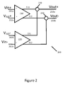
- FIG. 2 shows an example of a summing node 200 in accordance with examples. While the summing node 200 has been exemplified as being implemented in a delta-sigma modulator as an ELD summing node, it will be appreciated that the summing node 200 may be implemented in other applications where the summing speed of two differential input signals is of interest. The output of the summing node 200 may be provided to a non-linear element.
- Figure 2 shows a summing node 200 comprising a first differential amplifier having a first (non-inverting) and second (inverting) input and a second differential amplifier 220 having a third (non-inverting) and fourth (inverting) input.
- the summing node 200 is configured to receive a first differential signal 201 (V in ) comprising a direct signal (V in+ ) 201 a and an inverse signal (V in- ) 201 b.
- the direct signal 201 a is coupled or provided to the first (non-inverting) input of the first differential amplifier 210.
- the inverse signal 201 b is coupled or provided to a fourth (inverting) input of the second differential amplifier 220.
- the summing node 200 is further configured to receive a second differential signal (V ELD ) comprising a direct signal (V ELD +) 202a and an inverse signal (V ELD -) 202b.
- V ELD second differential signal
- the direct signal 202a is coupled or provided to the second (inverting) input of the first differential amplifier 210 and the inverse signal 202b is coupled or provided to the third (non-inverting) input of the second differential amplifier 220.
- the first differential amplifier 210 comprises a first output 211 and a second output 212 and the second differential amplifier 220 comprises a third output 221 and a fourth output 222.
- the first output 211 and the third output 221 are summed at adder 230 to provide a direct signal 250a of a differential output signal pair 250 (Vout).
- the second output 212 and the fourth output 222 are summed at adder 240 to provide an inverse signal 250b of the differential output signal pair 250. It will be appreciated that the inverse output signal 250b may be the compliment of the direct output signal 250a.
- the first differential amplifier 210 will output a differential output 211 and 212 corresponding to the difference between the direct signal components 201 a and 202a of the first and second differential input signal pairs (V in+ and V ELD +).
- the second differential amplifier 220 will output a differential output 221 and 222 corresponding to the difference between the inverse components 201 b and 202b of the first and second differential input signal pairs (V in- and V ELD -).
- the direct signal components 211 and 221 of the output of the differential amplifiers and the inverse signal components 212 and 222 of the output of the differential amplifiers are summed respectively to provide a direct output signal component 250a and an inverse output signal component 250b that is the compliment to the direct output signal component 250a.
- the summing node 200 and the amplifier 121 has been depicted as separate entities. However, it will be appreciated that the summing node 200 of figure 2 may carry out both the function of a summing node and the function of amplifier 121.
- the amplifiers 210, 220 may provide an amplified differential output. In the example with reference to figure 3 , this amplification is provided by the g m of the transistors used to implement the differential amplifiers 210 and 220.
- Figure 3 is an example implementation of summing node 200 using differential transistor pairs to provide the first and second differential amplifier 210 and 220 of figure 2 . It will be appreciated that figure 3 shows a specific example implementation using n-channel metal oxide field effect semiconductor transistors (MOSFETS) however it will be appreciated that other types of transistors may be used to implement the differential amplifier pairs.
- MOSFETS metal oxide field effect semiconductor transistors
- Figure 3 shows a first differential transistor pair 210 comprising a first transistor 311 (M1) and a second transistor 312 (M2).
- a gate terminal or input of the first transistor 311 is coupled to the direct signal component 201 a of the first differential input signal 201.
- a gate terminal or input of the second transistor 312 is coupled to the direct signal component 202a of the second differential input signal 202.
- Respective source terminals of the first and second transistors 311 and 312 are coupled to a bias current source 310.
- the summing node 200 further comprises a first and second load 351 and 352. It will be appreciated that the first and second load 351 and 352 may be any suitable load, for example they may be resistors or current sources. Drain terminals of the first and second transistors 311 and 312 are coupled to first terminals of the respective loads 351 and 352.
- Figure 3 further shows a second differential transistor pair 220 comprising a third transistor 321 (M3) and a fourth transistor 322 (M4).
- a gate terminal or input of the third transistor 321 is coupled to the inverse signal component 202b of the second differential input signal 202.
- a gate terminal input of the fourth transistor 322 is coupled to the inverse signal component 201 b of the first differential input signal 201.
- Respective source terminals of the third and fourth transistors 321 and 322 are coupled to a current source 320. Drain terminals of the third and fourth transistors 321 and 322 are coupled to the first terminals of the respective loads 351 and 352.
- the coupling point of the first terminal of the first load 351 and the drain terminals of the first transistor 311 and the third transistor 321 forms a first node 330.
- the coupling point of the first terminal of the second load 351 and the drain terminals of the second transistor 312 and the fourth transistor 322 forms a second node 340.
- the direct signal component 250a of the differential output signal 250 may be output from the first node 330 and the inverse signal component 250b of the differential output signal 250 may be output from the second node 340.
- the differential transistor pairs 210 and 220 may be as symmetrical as possible.
- the differential transistor pairs may be matched.
- the first to fourth transistors 311, 312, 321 and 322 may be selected to be as similar to each other as possible in transistor characteristics.
- the biasing of the first and second transistor pairs may be proportional.
- the first and second loads 351 and 352 may have the same value and the current sources may have a fixed relationship.
- the current source 320 may be a multiple of the current source 310. This multiplication factor may be set by system level simulations.
- the gate inputs of the pair of transistors determines the proportion of the current provided by the current source 310, 320 that may be provided to the respective load 351, 352 through that transistor.
- the input 201 a to the first transistor 311 and the input 202a to the second transistor control the functioning of the first and second transistors 311 and 312 to proportionally split the current (provided by current source 310) that each of the transistors can pull through their respective loads 351, 352.
- the inputs 202b and 201 b to the third and fourth transistors 321 and 322 control the proportion of the current (provided by current source 320) that can be pulled through the respective loads.
- the value at the first node 330 may thus correspond to the proportion of the current 310 pulled through the first transistor 311 plus the proportion of the current 320 pulled through the third transistor 321.
- the output at the first node may correspond and/or be proportional to the sum of the direct signal of the first differential signal V in+ 201 a and the indirect signal of the second differential signal V eld- 202b.
- the value at the second node 340 may thus correspond to the proportion of the current 310 pulled through the second transistor 312 plus the proportion of the current 320 pulled through the fourth transistor 322.
- the output at the second node may correspond and/or be proportional to the sum of the direct signal of the second differential signal V eld+ 202a and the indirect signal of the first differential signal Vin - 201b.
- difference between the output of the first node 330 and the output of the second node 340 may correspond to the difference between the first differential signal 201 and the second differential signal 202.
- the common mode input voltage of the transistors can be considered to be V cm .
- V in + V cm + ⁇ V in / 2
- V in - V cm - ⁇ V in / 2
- ⁇ V in is the first differential input signal 201
- V in+ 201a is the direct signal component of the first differential input signal 201
- V in- 201b is the inverse signal component of the first differential input signal 201
- V cm is the input common mode voltage
- V eld + V cm + ⁇ V eld / 2
- V eld - V cm - ⁇ V eld / 2
- ⁇ V eld is the second differential input signal 202
- V eld+ 202a is the direct signal component of the second differential input signal 202
- V eld- 202b is the inverse signal component of the second differential input signal 202
- V cm is the input common mode voltage
- Examples of the present disclosure may implement a summing node using two differential transistor pairs where the first differential transistor pair is configured to receive the direct signal components from the first and second differential input signals and the second differential transistor pair is configured to receive the inverse signal components of the first and second differential input signal.
- the arrangement of the inputs to the first and second differential transistor pairs may lead to the summing node having a higher linearity at a higher speed (sampling rate) than some other summing nodes. This will be discussed below.
- a summing node may comprise a first differential transistor pair (M1 and M2) having the direct and inverse signal components of a first differential input signal as inputs and a second differential transistor pair (M3 and M4) having the direct and inverse signal components of a second differential input signal as inputs.
- the differential voltage signal ⁇ V in at the input to the first transistor pair can be converted to a differential input current by multiplying it with the effective transconductance of the transistors M1 and M2 of the first transistor pair.
- the differential voltage signal ⁇ V eld at the input to the second transistor pair can be converted to a differential input current by multiplying it with the effective transconductance of the transistors M3 and M4 of the second transistor pair.
- I M1 / M2_differential is the differential current through the first transistor pair due to the differential voltage ⁇ V in at the inputs of M1 and M2
- I M3 / M4_differential is the differential current through the second transistor pair due to the differential voltage ⁇ V eld at the inputs of M3 and M4.
- equations 7 and 8 for a summing node that has a first differential signal as input into a first transistor pair and a second differential as input into a second differential pair, if the magnitude of the signals ⁇ V in and ⁇ V eld are in the range of 100mV and 50mV respectively, this may make the transconductance ' g m ' nonlinear thus introducing the nonlinearity in current summation.
- ⁇ V in is the first differential input signal 201
- ⁇ V eld is the second differential input signal 202 and the common mode input voltage V cm cancels out.
- the transistor pairs 311 and 312, and 321 and 322 are matched and so the transconductance of each pair is g m .
- the summing node 200 of the foregoing examples may be used in any application where differential input signals are to be subtracted and the result provided to a non-linear element such as a quantizer.
- a specific implementation of such a summing node 200 may be of use in a delta-sigma modulator, such as the one discussed in relation to figure 1 .
- the summing node 200 may provide a summing node for an excess loop delay (ELD) feedback from the output 102 of the delta-sigma modulator to the input of the quantizer 120.
- Figure 4 shows an example of the generation of the ELD differential signal (second differential signal 202) that may be input into the summing node 200.
- Figure 4 shows a differential output signal 205 from the quantizer 120.
- This signal 205 may correspond to signal 102 shown in figure 1 .
- a direct signal component 205a of the differential output signal 205 is coupled to a first inverter 401.
- the output of the first inverter 401 is coupled to a first terminal of a first resistor 403.
- a second terminal of the first resistor 403 is coupled to provide the direct signal component 202a of the second differential signal 202a.
- An inverse signal component 205b is coupled to the input of a second inverter 402.
- An output of the second inverter 402 is coupled to a first terminal of a second resistor 404.
- a second terminal of the second resistor 404 is coupled to provide the inverse signal component 202b of the second differential signal.
- a first terminal of a third resistor 405 is coupled to the second terminal of the first resistor 403.
- a second terminal of the third resistor 405 is coupled to the second terminal of the second resistor 404.
- the second terminal of the first resistor 403 is coupled to a first signal source 406.
- the second terminal of the second resistor 404 is coupled to a second signal source 407.
- the first and second signal sources 406 and 407 may be arranged so that the second signal source 407 is the inverse or compliment of the first signal source 406.
- the first and second signal sources 406 and 407 may be configured to introduce dither into the direct and inverse signal components 202a and 202b of the second differential input signal 202.
- the dither may be added to randomise third order tones due to square wave output from 122 at expense of increased noise in the wanted band.
- figure 1 depicts a first order delta-sigma modulator
- examples may be applicable to higher order modulators.
Landscapes
- Engineering & Computer Science (AREA)
- Power Engineering (AREA)
- Theoretical Computer Science (AREA)
- Physics & Mathematics (AREA)
- Nonlinear Science (AREA)
- Compression, Expansion, Code Conversion, And Decoders (AREA)
- Amplifiers (AREA)
Abstract
Description
- The present disclosure relates to a summing node in a delta-sigma modulator in particular, but not exclusively, for use in an analog to digital converter.
- Delta-sigma modulators can be considered to be a suitable architecture for medium bandwidth analog-to-digital converters (ADC) due to their tendencies toward linearity and power efficiency. However, the delta-sigma modulator is often clocked at high sampling rates which may introduce instability into the delta-sigma loop.
- Implementations that address loop instability are of interest.
- According to a first aspect, there is provided a summing node for summing a first and second differential signal, each comprising a direct and an inverse signal component; the summing node comprising: a first differential transistor pair comprising a first and second input and coupled to a first and second output; and a second differential transistor pair comprising a third and fourth input and coupled to the first and second output; wherein the first and fourth inputs are respectively coupled to the direct and inverse signal components of the first differential signal and the second and third inputs are respectively coupled to the direct and inverse signal components of the second differential signal.
- The first output may be configured to output a signal corresponding to the sum of the direct signal component of the first differential signal and the inverse signal component of the second differential signal. The second output may be configured to output signal corresponding to a sum of the direct signal component of the second differential signal and the inverse signal component of the first differential signal. The summing node may further comprise a first load coupled to the first output and a second load coupled to the second output. The first and second transistor pairs may be matched. The first and second loads may be matched. The first and second differential transistor pairs may have proportional biasing. The second output may be the compliment of the first output. The first and second output may be coupled to a non-linear element. The non-linear element may be a quantizer.
- According to a second aspect, there is provided a delta-sigma modulator comprising a summing node in accordance with the first aspect, wherein the first differential signal is output from a loop filter of the delta-sigma modulator and the second differential signal is an excess loop delay feedback signal from the output of the delta-sigma modulator.
- According to a third aspect, there is provided a method comprising summing a first and second differential signal, each of the first and second differential signals comprising a direct and an inverse signal component; the summing comprising: providing the respective direct signal components as inputs to a first differential transistor pair coupled to a first and second output; and providing the respective indirect signal components as inputs to a second differential transistor pair coupled to the first and second output.
- The method may further comprise: providing a signal corresponding to the sum of the direct signal component of the first differential signal and the inverse signal component of the second differential signal at the first output. The method may further comprise: providing a signal corresponding to a sum of the direct signal component of the second differential signal and the inverse signal component of the first differential signal at the second output. A first load may be coupled to the first output and a second load may be coupled to the second output.
-
-
Figure 1 shows an example schematic of a delta-sigma modulator; -
Figure 2 shows an example schematic of a summing node; -
Figure 3 shows an example circuit diagram of a summing node; and -
Figure 4 shows an example of an excess loop delay feedback loop. -
Figure 1 is an example of a delta-sigma modulator 100 that may be implemented in, for example, an analog-to-digital converter (ADC). It will be appreciated that delta-sigma modulators may be used in both analog-to-digital (ADC) and digital-to-analog converters (DAC). -
Figure 1 comprises aninput 101 for receiving an analog input signal and anoutput 102 for providing a digital output bit stream. Theanalog input signal 101 is input into a non-inverting input (+) of asumming node 103. The digitaloutput bit stream 102 is input to a digital-to-analog converter (DAC) 130 in a feedback loop to the inverting input (-) of thesumming node 103. Thus, the output of theDAC 130 is coupled to the inverting input (-) of thesumming node 103. - An output of the
summing node 103 is input to aloop filter 110. The output of theloop filter 110 is input to the non-inverting input (+) of an excess loop delay (ELD)summing node 200. The inverting input (-) of theELD summing node 200 is coupled to the output of an ELD digital-to-analog converter (DAC) 140. The input of the ELDDAC 140 is coupled to theoutput bit stream 102 and forms an excess loop delay feedback from theoutput bit stream 102 to theELD summing node 200. - An output of the
ELD summing node 200 is input to thequantizer 120. Thequantizer 120 comprises anamplifier 121 and acomparator 122. An input of theamplifier 121 is coupled to the output of theELD summing node 200 and the output of theamplifier 121 is coupled to an input of thecomparator 122. An output of thecomparator 122 provides theoutput bit stream 102. - The delta-
sigma modulator 100 may form part of an analog-to-digital converter. In this case theoutput bit stream 102 would be de-multiplexed and subsequently digitally low-pass filtered in order to provide a digital bit stream. - The
output bit stream 102 may be a one bit stream comprising high and low values, the average of which represents the analog input signal. Thebit stream 102 may be feedback through theDAC 130 and subtracted from theanalog input signal 101 to determine whether the analog input signal is increasing or decreasing with respect to its previous value. Theloop filter 110 may act as an integrator to integrate this difference which is then quantized. If, for example, theinput signal 101 is increasing with respect to its previous value, thequantizer 120 will output a high value (a logical 1) in order to increase the average of thebit stream 102. If theinput signal 101 is decreasing with respect to its average value, thequantizer 122 may output a low (logical 0) to decrease the average of thebit stream 102. - While some conventional ADC's may require a sample rate of more than twice the highest input signal frequency, delta-sigma modulators require a much higher sampling rate in order to produce a sufficient number of bit stream pulses on the
output bit stream 102 to provide a better approximation of theinput signal 101 by the averaging theoutput bit stream 102. Due to this high sampling rate, loop stability may become a serious issue. This loop stability may be affected, at least in part, by a delay introduced by thequantizer 120. In order to address loop stability, an excess loop delay (ELD) path may be implemented, for example the path provided by theELD DAC 140 andELD summing node 200 infigure 1 . - Examples of the present disclosure are directed to implementing a differential signal summing node that may be suitable for applications where the summing speed of the node may be of interest. In some examples, the summing node may be used to provide the
summing node 200 offigure 1 , however it will be appreciated that the summing node may be implemented to sum any two differential signals. In particular, the summing node may be used to sum two differential signals where the output is provided to a non-linear entity such as, for example, a quantizer. - In examples, the summing node may be provided by two differential amplifiers where the first differential amplifier receives, as inputs, direct signals of a first and second differential signal pair and the second amplifier receives, as inputs, the inverse signals of the first and second differential signal pairs. The direct signals output from the respective amplifier pairs may be summed to provide a direct output and the inverse signals output from the respective amplifier pairs may be summed to provide an inverse output. The inverse output of the summing node may be the compliment of the direct output.
-
Figure 2 shows an example of asumming node 200 in accordance with examples. While thesumming node 200 has been exemplified as being implemented in a delta-sigma modulator as an ELD summing node, it will be appreciated that thesumming node 200 may be implemented in other applications where the summing speed of two differential input signals is of interest. The output of thesumming node 200 may be provided to a non-linear element. -
Figure 2 shows asumming node 200 comprising a first differential amplifier having a first (non-inverting) and second (inverting) input and a seconddifferential amplifier 220 having a third (non-inverting) and fourth (inverting) input. Thesumming node 200 is configured to receive a first differential signal 201 (Vin) comprising a direct signal (Vin+) 201 a and an inverse signal (Vin-) 201 b. Thedirect signal 201 a is coupled or provided to the first (non-inverting) input of the firstdifferential amplifier 210. Theinverse signal 201 b is coupled or provided to a fourth (inverting) input of the seconddifferential amplifier 220. - The summing
node 200 is further configured to receive a second differential signal (VELD) comprising a direct signal (VELD+) 202a and an inverse signal (VELD-) 202b. Thedirect signal 202a is coupled or provided to the second (inverting) input of the firstdifferential amplifier 210 and theinverse signal 202b is coupled or provided to the third (non-inverting) input of the seconddifferential amplifier 220. - The first
differential amplifier 210 comprises afirst output 211 and asecond output 212 and the seconddifferential amplifier 220 comprises athird output 221 and afourth output 222. Thefirst output 211 and thethird output 221 are summed atadder 230 to provide adirect signal 250a of a differential output signal pair 250 (Vout). Thesecond output 212 and thefourth output 222 are summed atadder 240 to provide aninverse signal 250b of the differential output signal pair 250. It will be appreciated that theinverse output signal 250b may be the compliment of thedirect output signal 250a. - In operation, the first
differential amplifier 210 will output adifferential output direct signal components differential amplifier 220 will output adifferential output inverse components direct signal components inverse signal components output signal component 250a and an inverseoutput signal component 250b that is the compliment to the directoutput signal component 250a. - In
figure 1 , the summingnode 200 and theamplifier 121 has been depicted as separate entities. However, it will be appreciated that the summingnode 200 offigure 2 may carry out both the function of a summing node and the function ofamplifier 121. In particular, theamplifiers figure 3 , this amplification is provided by the gm of the transistors used to implement thedifferential amplifiers -
Figure 3 is an example implementation of summingnode 200 using differential transistor pairs to provide the first and seconddifferential amplifier figure 2 . It will be appreciated thatfigure 3 shows a specific example implementation using n-channel metal oxide field effect semiconductor transistors (MOSFETS) however it will be appreciated that other types of transistors may be used to implement the differential amplifier pairs. -
Figure 3 shows a firstdifferential transistor pair 210 comprising a first transistor 311 (M1) and a second transistor 312 (M2). A gate terminal or input of thefirst transistor 311 is coupled to thedirect signal component 201 a of the first differential input signal 201. A gate terminal or input of thesecond transistor 312 is coupled to thedirect signal component 202a of the second differential input signal 202. Respective source terminals of the first andsecond transistors current source 310. The summingnode 200 further comprises a first andsecond load second load second transistors respective loads -
Figure 3 further shows a seconddifferential transistor pair 220 comprising a third transistor 321 (M3) and a fourth transistor 322 (M4). A gate terminal or input of thethird transistor 321 is coupled to theinverse signal component 202b of the second differential input signal 202. A gate terminal input of thefourth transistor 322 is coupled to theinverse signal component 201 b of the first differential input signal 201. Respective source terminals of the third andfourth transistors current source 320. Drain terminals of the third andfourth transistors respective loads - The coupling point of the first terminal of the
first load 351 and the drain terminals of thefirst transistor 311 and thethird transistor 321 forms afirst node 330. The coupling point of the first terminal of thesecond load 351 and the drain terminals of thesecond transistor 312 and thefourth transistor 322 forms asecond node 340. Thedirect signal component 250a of the differential output signal 250 may be output from thefirst node 330 and theinverse signal component 250b of the differential output signal 250 may be output from thesecond node 340. - The differential transistor pairs 210 and 220 may be as symmetrical as possible. For example the differential transistor pairs may be matched. For example, the first to
fourth transistors second loads current source 320 may be a multiple of thecurrent source 310. This multiplication factor may be set by system level simulations. - For each
transistor pair current source respective load first transistor pair 210, theinput 201 a to thefirst transistor 311 and theinput 202a to the second transistor control the functioning of the first andsecond transistors respective loads inputs fourth transistors - The value at the
first node 330 may thus correspond to the proportion of the current 310 pulled through thefirst transistor 311 plus the proportion of the current 320 pulled through thethird transistor 321. In other words, the output at the first node may correspond and/or be proportional to the sum of the direct signal of the firstdifferential signal V in+ 201 a and the indirect signal of the seconddifferential signal V eld- 202b. Similarly the value at thesecond node 340 may thus correspond to the proportion of the current 310 pulled through thesecond transistor 312 plus the proportion of the current 320 pulled through thefourth transistor 322. In other words, the output at the second node may correspond and/or be proportional to the sum of the direct signal of the seconddifferential signal V eld+ 202a and the indirect signal of the firstdifferential signal Vin - 201b. - It will be appreciated that difference between the output of the
first node 330 and the output of thesecond node 340 may correspond to the difference between the first differential signal 201 and the second differential signal 202. - Referring to the example of
figure 3 , the common mode input voltage of the transistors can be considered to be Vcm. - We can write:


V in+ 201a is the direct signal component of the first differential input signal 201,V in- 201b is the inverse signal component of the first differential input signal 201, and Vcm is the input common mode voltage. - Also,


V eld+ 202a is the direct signal component of the second differential input signal 202,V eld- 202b is the inverse signal component of the second differential input signal 202, and Vcm is the input common mode voltage. - Examples of the present disclosure may implement a summing node using two differential transistor pairs where the first differential transistor pair is configured to receive the direct signal components from the first and second differential input signals and the second differential transistor pair is configured to receive the inverse signal components of the first and second differential input signal.
- The arrangement of the inputs to the first and second differential transistor pairs may lead to the summing node having a higher linearity at a higher speed (sampling rate) than some other summing nodes. This will be discussed below.
- In contrast, in some delta-sigma modulators, a summing node may comprise a first differential transistor pair (M1 and M2) having the direct and inverse signal components of a first differential input signal as inputs and a second differential transistor pair (M3 and M4) having the direct and inverse signal components of a second differential input signal as inputs. For the case of these contrasting delta-sigma modulators, the following can be written:
- The differential voltage signal present at inputs of the first differential transistor pair (M1/M2) is:

- The differential voltage signal present at inputs of the second differential transistor pair (M3/M4) is:

- The differential voltage signal ΔVin at the input to the first transistor pair can be converted to a differential input current by multiplying it with the effective transconductance of the transistors M1 and M2 of the first transistor pair. The differential voltage signal ΔVeld at the input to the second transistor pair can be converted to a differential input current by multiplying it with the effective transconductance of the transistors M3 and M4 of the second transistor pair.
- If the system is assumed to be perfectly matched, the transconductance of the transistors M1 and M2, M3 and M4 are equal to gm and the following holds:


- Considering an example case of equations 7 and 8 for a summing node that has a first differential signal as input into a first transistor pair and a second differential as input into a second differential pair, if the magnitude of the signals ΔVin and ΔVeld are in the range of 100mV and 50mV respectively, this may make the transconductance 'gm ' nonlinear thus introducing the nonlinearity in current summation.
- Referring to the example of the present disclosure and in particular the example of
figure 3 following from equations 1 to 4, the differential voltage signal present at inputs of the first differential transistor pair 210 (equation 9) and the second differential transistor pair 220 (equation 10):

- The transistor pairs 311 and 312, and 321 and 322 are matched and so the transconductance of each pair is gm. The differential current through each
pair 

differential transistor pair 210 and I M3/M4_differential is the differential current through the seconddifferential transistor pair 220. If the magnitude of the signals ΔVin and ΔVeld are in the range of 100mV and 50mV respectively, then (ΔVin - ΔVeld)/2 = 25mV. Thus the transconductance in equations 11 and 12 is multiplied by a lower factor than the transconductance in equations 7 and 8. The differential voltage signal present at inputs of the firstdifferential transistor pair 210 and the seconddifferential transistor pair 220 is less than if the inputs of the first differential transistor pair was coupling to the first differential input signal and the inputs of the second differential transistor pair were coupled to the second differential input signal. Linearity of the summingnode 200 may be achieved around the input common mode. - It will be appreciated that the summing
node 200 of the foregoing examples may be used in any application where differential input signals are to be subtracted and the result provided to a non-linear element such as a quantizer. As discussed, a specific implementation of such a summingnode 200 may be of use in a delta-sigma modulator, such as the one discussed in relation tofigure 1 . In particular, the summingnode 200 may provide a summing node for an excess loop delay (ELD) feedback from theoutput 102 of the delta-sigma modulator to the input of thequantizer 120.Figure 4 shows an example of the generation of the ELD differential signal (second differential signal 202) that may be input into the summingnode 200. -
Figure 4 shows a differential output signal 205 from thequantizer 120. This signal 205 may correspond to signal 102 shown infigure 1 . Adirect signal component 205a of the differential output signal 205 is coupled to afirst inverter 401. The output of thefirst inverter 401 is coupled to a first terminal of afirst resistor 403. A second terminal of thefirst resistor 403 is coupled to provide thedirect signal component 202a of the seconddifferential signal 202a. Aninverse signal component 205b is coupled to the input of asecond inverter 402. An output of thesecond inverter 402 is coupled to a first terminal of asecond resistor 404. A second terminal of thesecond resistor 404 is coupled to provide theinverse signal component 202b of the second differential signal. A first terminal of athird resistor 405 is coupled to the second terminal of thefirst resistor 403. A second terminal of thethird resistor 405 is coupled to the second terminal of thesecond resistor 404. The second terminal of thefirst resistor 403 is coupled to afirst signal source 406. The second terminal of thesecond resistor 404 is coupled to asecond signal source 407. - The first and
second signal sources second signal source 407 is the inverse or compliment of thefirst signal source 406. The first andsecond signal sources inverse signal components - It will be appreciated that while
figure 1 depicts a first order delta-sigma modulator, examples may be applicable to higher order modulators. - While examples of the present disclosure have been described in relation to delta-sigma modulation, it will be appreciated that examples are applicable to the summation of other pairs of differential signal, in particular examples may be applicable to the summing of differential signals at the input of a non-linear element, for example a quantizer.
- It will be readily understood that the components of the embodiments as generally described herein and illustrated in the appended figures could be arranged and designed in a wide variety of different configurations. Thus, the following more detailed description of various embodiments, as represented in the figures, is not intended to limit the scope of the present disclosure, but is merely representative of various embodiments. While the various aspects of the embodiments are presented in drawings, the drawings are not necessarily drawn to scale unless specifically indicated.
- The described embodiments are to be considered in all respects only as illustrative and not restrictive. The scope of the invention is, therefore, indicated by the appended claims rather than by this detailed description. All changes that come within the meaning and range of equivalency of the claims are to be embraced within their scope.
- Reference throughout this specification to features, advantages, or similar language does not imply that all of the features and advantages that may be realized with the present invention should be or are in any single embodiment. Rather, language referring to the features and advantages is understood to mean that a specific feature, advantage, or characteristic described in connection with an embodiment is included in at least one embodiment. Thus, discussions of the features and advantages, and similar language, throughout this specification may, but do not necessarily, refer to the same embodiment.
- Furthermore, the described features, advantages, and characteristics of the invention may be combined in any suitable manner in one or more embodiments. One skilled in the relevant art will recognize, in light of the description herein, that the invention can be practiced without one or more of the specific features or advantages of a particular embodiment. In other instances, additional features and advantages may be recognized in certain embodiments that may not be present in all embodiments of the invention.
- Reference throughout this specification to an example or embodiment, or similar language means that a particular feature, structure, or characteristic described in connection with the indicated embodiment is included in at least one embodiment. Thus, the phrases "in one example" "in an example" and similar language throughout this specification may, but do not necessarily, all refer to the same embodiment.
Claims (15)
- A summing node for summing a first and second differential signal, each comprising a direct and an inverse signal component; the summing node comprising:a first differential transistor pair comprising a first and second input and coupled to a first and second output; anda second differential transistor pair comprising a third and fourth input and coupled to the first and second output;wherein the first and fourth inputs are respectively coupled to the direct and inverse signals components of the first differential signal and the second and third inputs are respectively coupled to the direct and inverse signals components of the second differential signal.
- The summing node of claim 1 wherein the first output is configured to output a signal corresponding to the sum of the direct signal component of the first differential signal and the inverse signal component of the second differential signal.
- The summing node of any preceding claim wherein the second output is configured to output a signal corresponding to a sum of the direct signal component of the second differential signal and the inverse signal component of the first differential signal.
- The summing node of any preceding claim comprising a first load coupled to the first output and a second load coupled to the second output.
- The summing node of any preceding claim wherein the first and second transistor pairs are matched.
- The summing node of claim 5 when dependent on claim 4 wherein the first and second load are matched.
- The summing node of claim 5 wherein the first and second differential transistor pair have proportional biasing.
- The summing node of any preceding claim where the second output is the compliment of the first output
- The summing node of any preceding claim wherein the first and second output are coupled to a non-linear element.
- The summing node of claim 9 wherein the non-linear element is a quantizer.
- A delta-sigma modulator comprising a summing node in accordance with any of the claims 1 to 10, wherein the first differential signal is output from a loop filter of the delta-sigma modulator and the second differential signal is an excess loop delay feedback signal from the output of the delta-sigma modulator.
- A method comprising summing a first and second differential signal, each of the first and second differential signals comprising a direct and an inverse signal component; the summing comprising:providing the respective direct signal components as inputs to a first differential transistor pair coupled to a first and second output; andproviding the respective indirect signal components as inputs to a second differential transistor pair coupled to the first and second output.
- The method of claim 12 further comprising:providing a signal corresponding to the sum of the direct signal component of the first differential signal and the inverse signal component of the second differential signal at the first output.
- The method of any of claims 12 and 13 further comprising:providing a signal corresponding to a sum of the direct signal component of the second differential signal and the inverse signal component of the first differential signal at the second output.
- The method of any of claims 12 to 14 wherein a first load is coupled to the first output and a second load is coupled to the second output.
Priority Applications (3)
| Application Number | Priority Date | Filing Date | Title |
|---|---|---|---|
| EP15195360.1A EP3171514A1 (en) | 2015-11-19 | 2015-11-19 | Differential summing node |
| US15/342,009 US20170149388A1 (en) | 2015-11-19 | 2016-11-02 | Differential summing node |
| CN201610979786.5A CN107046427A (en) | 2015-11-19 | 2016-11-08 | Difference summing junction |
Applications Claiming Priority (1)
| Application Number | Priority Date | Filing Date | Title |
|---|---|---|---|
| EP15195360.1A EP3171514A1 (en) | 2015-11-19 | 2015-11-19 | Differential summing node |
Publications (1)
| Publication Number | Publication Date |
|---|---|
| EP3171514A1 true EP3171514A1 (en) | 2017-05-24 |
Family
ID=54601690
Family Applications (1)
| Application Number | Title | Priority Date | Filing Date |
|---|---|---|---|
| EP15195360.1A Withdrawn EP3171514A1 (en) | 2015-11-19 | 2015-11-19 | Differential summing node |
Country Status (3)
| Country | Link |
|---|---|
| US (1) | US20170149388A1 (en) |
| EP (1) | EP3171514A1 (en) |
| CN (1) | CN107046427A (en) |
Families Citing this family (1)
| Publication number | Priority date | Publication date | Assignee | Title |
|---|---|---|---|---|
| US20260066919A1 (en) * | 2024-09-04 | 2026-03-05 | Nxp B.V. | High-Speed Continuous-Time Delta-Sigma Modulator Including an Amplifier with Limited Gain |
Citations (1)
| Publication number | Priority date | Publication date | Assignee | Title |
|---|---|---|---|---|
| US7375559B1 (en) * | 2005-07-07 | 2008-05-20 | Marvell International Ltd. | Differential comparator with a replica input stage to set the accurate bias current for improved common mode rejection |
Family Cites Families (6)
| Publication number | Priority date | Publication date | Assignee | Title |
|---|---|---|---|---|
| US5729230A (en) * | 1996-01-17 | 1998-03-17 | Hughes Aircraft Company | Delta-Sigma Δ-Σ modulator having a dynamically tunable continuous time Gm-C architecture |
| US6624688B2 (en) * | 2002-01-07 | 2003-09-23 | Intel Corporation | Filtering variable offset amplifer |
| KR100725994B1 (en) * | 2005-09-06 | 2007-06-08 | 삼성전자주식회사 | Low power multi-level pulse amplitude modulation driver and semiconductor device comprising said driver |
| DE102006004212B4 (en) * | 2006-01-30 | 2009-09-24 | Xignal Technologies Ag | Delta-sigma analog-to-digital converters and methods for delta-sigma analog-to-digital conversion with offset compensation |
| US8514117B2 (en) * | 2011-09-09 | 2013-08-20 | Texas Instruments Incorporated | Excess loop delay compensation for a continuous time sigma delta modulator |
| US8791848B2 (en) * | 2012-02-22 | 2014-07-29 | Mediatek Inc. | Sigma-delta modulators with excess loop delay compensation |
-
2015
- 2015-11-19 EP EP15195360.1A patent/EP3171514A1/en not_active Withdrawn
-
2016
- 2016-11-02 US US15/342,009 patent/US20170149388A1/en not_active Abandoned
- 2016-11-08 CN CN201610979786.5A patent/CN107046427A/en active Pending
Patent Citations (1)
| Publication number | Priority date | Publication date | Assignee | Title |
|---|---|---|---|---|
| US7375559B1 (en) * | 2005-07-07 | 2008-05-20 | Marvell International Ltd. | Differential comparator with a replica input stage to set the accurate bias current for improved common mode rejection |
Non-Patent Citations (2)
| Title |
|---|
| VIPUL KATYAL ET AL: "A New High Precision Low Offset Dynamic Comparator for High Resolution High Speed ADCs", CIRCUITS AND SYSTEMS, 2006. APCCAS 2006. IEEE ASIA PACIFIC CONFERENCE ON, IEEE, PISCATAWAY, NJ, USA, 1 December 2006 (2006-12-01), pages 5 - 8, XP031070760, ISBN: 978-1-4244-0387-5 * |
| ZHANG BO ET AL: "A 40 nm CMOS 195 mW/55 mW Dual-Path Receiver AFE for Multi-Standard 8.5-11.5 Gb/s Serial L", IEEE JOURNAL OF SOLID-STATE CIRCUITS, IEEE SERVICE CENTER, PISCATAWAY, NJ, USA, vol. 50, no. 2, 1 February 2015 (2015-02-01), pages 426 - 439, XP011571315, ISSN: 0018-9200, [retrieved on 20150128], DOI: 10.1109/JSSC.2014.2364032 * |
Also Published As
| Publication number | Publication date |
|---|---|
| US20170149388A1 (en) | 2017-05-25 |
| CN107046427A (en) | 2017-08-15 |
Similar Documents
| Publication | Publication Date | Title |
|---|---|---|
| US8077066B2 (en) | ΔΣ modulator | |
| US7612608B2 (en) | Sigma-delta based Class D audio or servo amplifier with load noise shaping | |
| US8791848B2 (en) | Sigma-delta modulators with excess loop delay compensation | |
| US6369730B1 (en) | Sigma-delta analog-to-digital converter | |
| EP1936811A2 (en) | Sigma-delta modulators | |
| US10361668B2 (en) | Differential current to voltage converter | |
| US20080042745A1 (en) | Sigma-delta based class d audio power amplifier with high power efficiency | |
| US9143145B2 (en) | Delta-sigma modulator | |
| EP4113847A1 (en) | A sigma delta modulator and method therefor | |
| CN102124654B (en) | Oversampling A/D converter | |
| JPS6252963B2 (en) | ||
| US20190097647A1 (en) | Delta sigma modulator | |
| US10566993B2 (en) | Delta-sigma modulator and delta-sigma converter | |
| US20220407539A1 (en) | Sigma-delta analogue-to-digital converter with gmc-vdac | |
| US10790790B2 (en) | Amplifiers with delta-sigma modulators using pulse-density modulations and related processes | |
| EP3139502B1 (en) | Single-ended to differential conversion circuit and signal processing module | |
| US9806703B2 (en) | Single-ended to differential conversion circuit and signal processing module | |
| EP3171514A1 (en) | Differential summing node | |
| JP2000269761A (en) | Switching amplifier using ΔΣ modulation | |
| US8466822B2 (en) | Analog-to-digital conversion apparatus and signal processing system | |
| US7423566B2 (en) | Sigma-delta modulator using a passive filter | |
| US10135394B2 (en) | Low voltage supply amplifier and amplification method | |
| US5216354A (en) | Controllable voltage-to-current converter having third-order distortion reduction | |
| JPH0575362A (en) | Balanced amplifier | |
| EP1737128A2 (en) | Impedance conversion circuit and integrated circuit including the same |
Legal Events
| Date | Code | Title | Description |
|---|---|---|---|
| PUAI | Public reference made under article 153(3) epc to a published international application that has entered the european phase |
Free format text: ORIGINAL CODE: 0009012 |
|
| AK | Designated contracting states |
Kind code of ref document: A1 Designated state(s): AL AT BE BG CH CY CZ DE DK EE ES FI FR GB GR HR HU IE IS IT LI LT LU LV MC MK MT NL NO PL PT RO RS SE SI SK SM TR |
|
| AX | Request for extension of the european patent |
Extension state: BA ME |
|
| 17P | Request for examination filed |
Effective date: 20171124 |
|
| RBV | Designated contracting states (corrected) |
Designated state(s): AL AT BE BG CH CY CZ DE DK EE ES FI FR GB GR HR HU IE IS IT LI LT LU LV MC MK MT NL NO PL PT RO RS SE SI SK SM TR |
|
| STAA | Information on the status of an ep patent application or granted ep patent |
Free format text: STATUS: THE APPLICATION IS DEEMED TO BE WITHDRAWN |
|
| 18D | Application deemed to be withdrawn |
Effective date: 20180602 |