EP3171466A1 - Vertical cavity light emitting device - Google Patents
Vertical cavity light emitting device Download PDFInfo
- Publication number
- EP3171466A1 EP3171466A1 EP16199102.1A EP16199102A EP3171466A1 EP 3171466 A1 EP3171466 A1 EP 3171466A1 EP 16199102 A EP16199102 A EP 16199102A EP 3171466 A1 EP3171466 A1 EP 3171466A1
- Authority
- EP
- European Patent Office
- Prior art keywords
- layer
- current confinement
- transparent electrode
- opening
- vertical cavity
- Prior art date
- Legal status (The legal status is an assumption and is not a legal conclusion. Google has not performed a legal analysis and makes no representation as to the accuracy of the status listed.)
- Granted
Links
Images



Classifications
-
- H—ELECTRICITY
- H01—ELECTRIC ELEMENTS
- H01S—DEVICES USING THE PROCESS OF LIGHT AMPLIFICATION BY STIMULATED EMISSION OF RADIATION [LASER] TO AMPLIFY OR GENERATE LIGHT; DEVICES USING STIMULATED EMISSION OF ELECTROMAGNETIC RADIATION IN WAVE RANGES OTHER THAN OPTICAL
- H01S5/00—Semiconductor lasers
- H01S5/10—Construction or shape of the optical resonator, e.g. extended or external cavity, coupled cavities, bent-guide, varying width, thickness or composition of the active region
- H01S5/18—Surface-emitting [SE] lasers, e.g. having both horizontal and vertical cavities
- H01S5/183—Surface-emitting [SE] lasers, e.g. having both horizontal and vertical cavities having only vertical cavities, e.g. vertical cavity surface-emitting lasers [VCSEL]
- H01S5/18361—Structure of the reflectors, e.g. hybrid mirrors
-
- H—ELECTRICITY
- H01—ELECTRIC ELEMENTS
- H01S—DEVICES USING THE PROCESS OF LIGHT AMPLIFICATION BY STIMULATED EMISSION OF RADIATION [LASER] TO AMPLIFY OR GENERATE LIGHT; DEVICES USING STIMULATED EMISSION OF ELECTROMAGNETIC RADIATION IN WAVE RANGES OTHER THAN OPTICAL
- H01S5/00—Semiconductor lasers
- H01S5/0014—Measuring characteristics or properties thereof
- H01S5/0021—Degradation or life time measurements
-
- H—ELECTRICITY
- H01—ELECTRIC ELEMENTS
- H01S—DEVICES USING THE PROCESS OF LIGHT AMPLIFICATION BY STIMULATED EMISSION OF RADIATION [LASER] TO AMPLIFY OR GENERATE LIGHT; DEVICES USING STIMULATED EMISSION OF ELECTROMAGNETIC RADIATION IN WAVE RANGES OTHER THAN OPTICAL
- H01S5/00—Semiconductor lasers
- H01S5/04—Processes or apparatus for excitation, e.g. pumping, e.g. by electron beams
- H01S5/042—Electrical excitation ; Circuits therefor
- H01S5/0425—Electrodes, e.g. characterised by the structure
- H01S5/04252—Electrodes, e.g. characterised by the structure characterised by the material
- H01S5/04253—Electrodes, e.g. characterised by the structure characterised by the material having specific optical properties, e.g. transparent electrodes
-
- H—ELECTRICITY
- H01—ELECTRIC ELEMENTS
- H01S—DEVICES USING THE PROCESS OF LIGHT AMPLIFICATION BY STIMULATED EMISSION OF RADIATION [LASER] TO AMPLIFY OR GENERATE LIGHT; DEVICES USING STIMULATED EMISSION OF ELECTROMAGNETIC RADIATION IN WAVE RANGES OTHER THAN OPTICAL
- H01S5/00—Semiconductor lasers
- H01S5/10—Construction or shape of the optical resonator, e.g. extended or external cavity, coupled cavities, bent-guide, varying width, thickness or composition of the active region
- H01S5/18—Surface-emitting [SE] lasers, e.g. having both horizontal and vertical cavities
- H01S5/183—Surface-emitting [SE] lasers, e.g. having both horizontal and vertical cavities having only vertical cavities, e.g. vertical cavity surface-emitting lasers [VCSEL]
- H01S5/18308—Surface-emitting [SE] lasers, e.g. having both horizontal and vertical cavities having only vertical cavities, e.g. vertical cavity surface-emitting lasers [VCSEL] having a special structure for lateral current or light confinement
-
- H—ELECTRICITY
- H01—ELECTRIC ELEMENTS
- H01S—DEVICES USING THE PROCESS OF LIGHT AMPLIFICATION BY STIMULATED EMISSION OF RADIATION [LASER] TO AMPLIFY OR GENERATE LIGHT; DEVICES USING STIMULATED EMISSION OF ELECTROMAGNETIC RADIATION IN WAVE RANGES OTHER THAN OPTICAL
- H01S5/00—Semiconductor lasers
- H01S5/10—Construction or shape of the optical resonator, e.g. extended or external cavity, coupled cavities, bent-guide, varying width, thickness or composition of the active region
- H01S5/18—Surface-emitting [SE] lasers, e.g. having both horizontal and vertical cavities
- H01S5/183—Surface-emitting [SE] lasers, e.g. having both horizontal and vertical cavities having only vertical cavities, e.g. vertical cavity surface-emitting lasers [VCSEL]
- H01S5/18341—Intra-cavity contacts
-
- H—ELECTRICITY
- H01—ELECTRIC ELEMENTS
- H01S—DEVICES USING THE PROCESS OF LIGHT AMPLIFICATION BY STIMULATED EMISSION OF RADIATION [LASER] TO AMPLIFY OR GENERATE LIGHT; DEVICES USING STIMULATED EMISSION OF ELECTROMAGNETIC RADIATION IN WAVE RANGES OTHER THAN OPTICAL
- H01S2301/00—Functional characteristics
- H01S2301/17—Semiconductor lasers comprising special layers
- H01S2301/176—Specific passivation layers on surfaces other than the emission facet
-
- H—ELECTRICITY
- H01—ELECTRIC ELEMENTS
- H01S—DEVICES USING THE PROCESS OF LIGHT AMPLIFICATION BY STIMULATED EMISSION OF RADIATION [LASER] TO AMPLIFY OR GENERATE LIGHT; DEVICES USING STIMULATED EMISSION OF ELECTROMAGNETIC RADIATION IN WAVE RANGES OTHER THAN OPTICAL
- H01S5/00—Semiconductor lasers
- H01S5/0014—Measuring characteristics or properties thereof
-
- H—ELECTRICITY
- H01—ELECTRIC ELEMENTS
- H01S—DEVICES USING THE PROCESS OF LIGHT AMPLIFICATION BY STIMULATED EMISSION OF RADIATION [LASER] TO AMPLIFY OR GENERATE LIGHT; DEVICES USING STIMULATED EMISSION OF ELECTROMAGNETIC RADIATION IN WAVE RANGES OTHER THAN OPTICAL
- H01S5/00—Semiconductor lasers
- H01S5/04—Processes or apparatus for excitation, e.g. pumping, e.g. by electron beams
- H01S5/042—Electrical excitation ; Circuits therefor
- H01S5/0425—Electrodes, e.g. characterised by the structure
- H01S5/04256—Electrodes, e.g. characterised by the structure characterised by the configuration
-
- H—ELECTRICITY
- H01—ELECTRIC ELEMENTS
- H01S—DEVICES USING THE PROCESS OF LIGHT AMPLIFICATION BY STIMULATED EMISSION OF RADIATION [LASER] TO AMPLIFY OR GENERATE LIGHT; DEVICES USING STIMULATED EMISSION OF ELECTROMAGNETIC RADIATION IN WAVE RANGES OTHER THAN OPTICAL
- H01S5/00—Semiconductor lasers
- H01S5/10—Construction or shape of the optical resonator, e.g. extended or external cavity, coupled cavities, bent-guide, varying width, thickness or composition of the active region
- H01S5/18—Surface-emitting [SE] lasers, e.g. having both horizontal and vertical cavities
- H01S5/183—Surface-emitting [SE] lasers, e.g. having both horizontal and vertical cavities having only vertical cavities, e.g. vertical cavity surface-emitting lasers [VCSEL]
- H01S5/18308—Surface-emitting [SE] lasers, e.g. having both horizontal and vertical cavities having only vertical cavities, e.g. vertical cavity surface-emitting lasers [VCSEL] having a special structure for lateral current or light confinement
- H01S5/18322—Position of the structure
- H01S5/1833—Position of the structure with more than one structure
- H01S5/18333—Position of the structure with more than one structure only above the active layer
-
- H—ELECTRICITY
- H01—ELECTRIC ELEMENTS
- H01S—DEVICES USING THE PROCESS OF LIGHT AMPLIFICATION BY STIMULATED EMISSION OF RADIATION [LASER] TO AMPLIFY OR GENERATE LIGHT; DEVICES USING STIMULATED EMISSION OF ELECTROMAGNETIC RADIATION IN WAVE RANGES OTHER THAN OPTICAL
- H01S5/00—Semiconductor lasers
- H01S5/10—Construction or shape of the optical resonator, e.g. extended or external cavity, coupled cavities, bent-guide, varying width, thickness or composition of the active region
- H01S5/18—Surface-emitting [SE] lasers, e.g. having both horizontal and vertical cavities
- H01S5/183—Surface-emitting [SE] lasers, e.g. having both horizontal and vertical cavities having only vertical cavities, e.g. vertical cavity surface-emitting lasers [VCSEL]
- H01S5/18361—Structure of the reflectors, e.g. hybrid mirrors
- H01S5/18369—Structure of the reflectors, e.g. hybrid mirrors based on dielectric materials
-
- H—ELECTRICITY
- H01—ELECTRIC ELEMENTS
- H01S—DEVICES USING THE PROCESS OF LIGHT AMPLIFICATION BY STIMULATED EMISSION OF RADIATION [LASER] TO AMPLIFY OR GENERATE LIGHT; DEVICES USING STIMULATED EMISSION OF ELECTROMAGNETIC RADIATION IN WAVE RANGES OTHER THAN OPTICAL
- H01S5/00—Semiconductor lasers
- H01S5/30—Structure or shape of the active region; Materials used for the active region
- H01S5/34—Structure or shape of the active region; Materials used for the active region comprising quantum well or superlattice structures, e.g. single quantum well [SQW] lasers, multiple quantum well [MQW] lasers or graded index separate confinement heterostructure [GRINSCH] lasers
- H01S5/343—Structure or shape of the active region; Materials used for the active region comprising quantum well or superlattice structures, e.g. single quantum well [SQW] lasers, multiple quantum well [MQW] lasers or graded index separate confinement heterostructure [GRINSCH] lasers in AIIIBV compounds, e.g. AlGaAs-laser, InP-based laser
- H01S5/34333—Structure or shape of the active region; Materials used for the active region comprising quantum well or superlattice structures, e.g. single quantum well [SQW] lasers, multiple quantum well [MQW] lasers or graded index separate confinement heterostructure [GRINSCH] lasers in AIIIBV compounds, e.g. AlGaAs-laser, InP-based laser with a well layer based on Ga(In)N or Ga(In)P, e.g. blue laser
Definitions
- the present invention relates to a vertical cavity light emitting device, such as a vertical cavity surface emitting laser (VCSEL).
- VCSEL vertical cavity surface emitting laser
- a vertical cavity surface emitting laser is a type of semiconductor laser configured so that light is resonated vertically with respect to a substrate surface and emitted in a vertical direction to the substrate surface.
- Patent Literature 1 discloses a vertical cavity surface emitting laser having, on at least one surface of a nitride semiconductor layer, an insulation layer having an opening, a translucent electrode disposed on the insulation layer so as to cover the opening, and a reflecting mirror above the opening with the translucent electrode interposed therebetween.
- a vertical cavity light emitting device such as a vertical cavity surface emitting laser, has reflecting mirrors that are opposite to each other with a light emitting layer interposed therebetween, and these reflecting mirrors form a resonator or cavity.
- a reflecting mirror can be formed by alternately laminating two types of thin films with different refractive indexes.
- a reflecting mirror have high reflection characteristics. It is preferable that the current applied to the vertical cavity surface emitting laser be injected to a light emitting layer without loss.
- the present invention has been made in view of the foregoing problem. It is an object of the present invention to provide a vertical cavity light emitting device that can reduce the threshold current and enhance the manufacturing yield.
- a vertical cavity light emitting device including:
- a vertical cavity surface emitting laser (hereinafter also simply referred to as “surface emitting laser”), which is one example of the vertical cavity light emitting device according to the present invention, will now be described with reference to the drawings.
- surface emitting laser which is one example of the vertical cavity light emitting device according to the present invention
- the present inventor has focused on an opening portion of a current confinement layer that is an insulation layer. Also, the present inventor has researched and experimented the relationship between a side wall of the opening portion and the lasing threshold current of a surface emitting laser. As a result, the present inventor has found the structure capable of reducing the threshold current and reached the present invention.
- FIG. 1 is a perspective view schematically illustrating a configuration of a surface emitting laser 10 according to a first embodiment of the present invention.
- the surface emitting laser 10 includes an emission port EP of a laser beam BM.
- the surface emitting laser 10 has a resonant portion 20 formed on a semiconductor substrate 11.
- FIG. 2 is a partial cross-sectional view schematically illustrating a part of the surface emitting laser 10 along a line XX of FIG. 1 .
- a light emitting portion of the surface emitting laser 10 includes the resonant portion 20 formed on the conductive substrate 11 comprising GaN (gallium nitride), the resonant portion 20 including a conductive first multilayer film reflector 13; a semiconductor structure layer SEM; an insulating current confinement layer; a transparent electrode 23; a p-contact layer p-Co; and a second multilayer film reflector 25.
- the semiconductor structure layer SEM is constituted by a GaN semiconductor.
- An n-contact layer n-Co is formed on the surface opposite to the p-contact layer p-Co of the substrate 11.
- a through opening OP1 of the current confinement layer formed directly below the transparent electrode 23 of the resonant portion 20 corresponds to the emission port EP of the laser beam BM.
- the first multilayer film reflector 13 and the second multilayer film reflector 25 are each formed as a distributed Bragg reflector (DBR).
- the semiconductor structure layer SEM is interposed between the first multilayer film reflector 13 and the second multilayer film reflector 25 so as to define a resonator structure.
- the first multilayer film reflector 13 and the second multilayer film reflector 25 are formed by properly adjusting, for example, materials, film thicknesses, and the number of pairs of multilayer films.
- an insulating multilayer film reflector is formed from a dielectric multilayer film.
- Examples of the thin film materials for a reflector may include oxides of metals, semimetals, etc.; or nitrides, such as AlN, AlGaN, GaN, BN, and SiN.
- An insulating multilayer film reflector can be obtained by regularly and alternately laminating at least two dielectric thin films with different refractive indexes, such as SiO 2 /Nb 2 O 5 , SiO 2 /ZrO 2 , SiO 2 /AlN, and Al 2 O 3 /Nb 2 O 5 .
- FIG. 3 is a partial cross-sectional view schematically illustrating a part of the surface emitting laser 10 encircled by a dashed line Y of FIG. 2 .
- the semiconductor structure layer SEM is formed from layers on the first multilayer film reflector 13, i.e., an n-type semiconductor layer 15, an active layer 17 including a quantum well layer, and a p-type semiconductor layer 19, in this order.
- each layer of the first multilayer film reflector 13 and the semiconductor structure layer SEM has the composition of Al x In y Ga 1-x-y N (0 ⁇ x ⁇ 1, 0 ⁇ y ⁇ 1, 0 ⁇ x + y ⁇ 1).
- the structure of the first multilayer film reflector 13 is configured such that a low-refractive index semiconductor layer with the composition of AlInN and a high-refractive index semiconductor layer with the composition of GaN are alternately laminated to form a laminated structure of a plurality of pairs of the low-refractive index and high-refractive index semiconductor layers.
- the active layer 17 has a quantum well structure configured such that a well layer (not shown) with the composition of InGaN and a barrier layer (not shown) with the composition of GaN are alternately laminated to form a laminated structure of a plurality of pairs of the well layer and the barrier layer.
- the n-type semiconductor layer 15 has the composition of GaN and contains Si as an n-type impurity.
- the p-type semiconductor layer 19 has the composition of GaN and contains Mg, etc. as a p-type impurity.
- the n-type semiconductor layer 15 and the p-type semiconductor layer 19 are thereby of opposite conductivity types.
- a buffer layer (not shown) is formed between the substrate 11 and the first multilayer film reflector 13.
- the first multilayer film reflector 13 and the semiconductor structure layer SEM are formed using, for example, a metal organic chemical vapor deposition (MOCVD) method.
- MOCVD metal organic chemical vapor deposition
- the insulating current confinement layer 21 is formed on the p-type semiconductor layer 19 and has the through opening OP1.
- the transparent electrode 23 is formed over the current confinement layer 21 and the p-type semiconductor layer 19 so as to cover the through opening OP1 and to be in contact with the p-type semiconductor layer 19.
- the current confinement layer 21 allows a current to be injected from the transparent electrode 23 to the active laser 17 via the through opening OP1.
- the current confinement layer 21 blocks injection of a current through a portion other than the through opening OP1.
- FIG. 4 is a top plan view illustrating the configuration of the surface emitting laser 10 viewed from the beam radiation side.
- a mixed composition layer 24 including the composition (or components) of the current confinement layer 21 and the composition (or components) of the transparent electrode 23 is annularly formed at the position defining the current confinement layer 21, specifically, along the edge of the current confinement layer 21.
- the area of the annular mixed composition layer 24 is 1% to 20%, preferably 5% or more, the area of the through opening OP1 and can be properly adjusted by changing a below-described tapered angle ⁇ . As the tapered angle ⁇ decreases, the area of the mixed composition layer 24 increases.
- Examples of the component materials of the current confinement layer 21 may include: oxides, such as SiO 2 , Ga 2 O 3 , Al 2 O 3 , and ZrO 2 ; and nitrides, such as SiN, AlN, and AlGaN. It is preferable to use SiO 2 for the current confinement layer 21.
- the film thickness of the current confinement layer 21 is 5 to 1000 nm, and preferably 10 to 300 nm.
- Examples of the component materials of the transparent electrode 23 may include a conductive metal oxide such as ITO (Indium Tin Oxide), In 2 O 3 , IZO (In-doped ZnO), AZO (Al-doped ZnO), GZO (Ga-doped ZnO), ATO (Sb-doped SnO 2 ), FTO (F-doped SnO 2 ), NTO (Nb-doped TiO 2 ), and ZnO. It is preferable to use ITO for the transparent electrode 23.
- the film thickness of the transparent electrode 23 is 3 to 100 nm, and preferably 20 nm or smaller.
- the shape of the through opening OP1 is a circle with a diameter of 1 to 15 ⁇ m, and preferably 3 to 10 ⁇ m, so that a Gaussian beam can be obtained by maintaining the constant distance from the circle edge to the beam center.
- a current can be uniformly injected to the active layer 17, and a light beam can be uniformly confined.
- the shape of the through opening OP1 may be a non-circular shape, such as an ellipse or polygon, or a shape similar to a circle.
- the current confinement layer 21 has a tapered cross-sectional shape where the thickness decreases toward the mixed composition layer 24 (the edge of the through opening OP1).
- the tapered angle ⁇ of the tapered cross-sectional shape of the current confinement layer 21 preferably exceeds 0 degrees and is equal to or smaller than 45 degrees.
- the semiconductor structure layer SEM of the surface emitting laser 10 was designed in such a manner that the emission wavelength ranged from 400 to 450 nm.
- the first multilayer film reflector 13, which is an electrically-conducting mirror, was designed so as to include forty laminated pairs of GaN/InAlN.
- the second multilayer film reflector 25, which is a dielectric mirror, was designed so as to include eight laminated pairs of Nb 2 O 5 /SiO 2 .
- the predetermined semiconductor structure layer SEM was produced using the MOCVD method on a substrate.
- the SiO 2 current confinement layer 21 with a predetermined thickness on the p-GaN semiconductor layer 19 was subjected to etching or liftoff method to remove SiO 2 by means of chemical treatment only in the portion where the through opening OP1 (with an outer diameter of 10 ⁇ m) was to be formed.
- the edge portion of the current confinement layer 21 formed along the through opening OP1 by the liftoff method specifically has the tapered cross-section of FIG. 5 with the tapered angle ⁇ .
- an ITO transparent electrode with a predetermined thickness was formed by the electron beam deposition method on the current confinement layer 21 and over the through opening OP1.
- the p-contact layer p-Co and the second multilayer film reflector 25 were also formed, and, as illustrated in FIG. 6 , an incomplete surface emitting laser 10 without the mixed composition layer 24 was thus produced.
- FIG. 7 shows partial cross-sectional TEM images (a) and (b), which show an area near the edge portion of the through opening of the current confinement layer in the surface emitting laser before and after the excess pulse application treatment, respectively.
- a partially enlarged image of the interface portion shown by a dashed line in the left side image of each of (a) and (b) of FIG. 7 .
- FIG. 8 is a graph illustrating the results.
- the vertical axis of FIG. 8 represents the pulse threshold current (mA)
- the horizontal axis of FIG. 8 represents the current injection period (second) of the excess pulse application treatment.
- the threshold current can be controlled on the basis of the application time period of the excess pulse application treatment for generating the mixed composition layer 24.
- a uniform threshold current can be applied to a plurality of the surface emitting lasers 10 in a wafer during manufacturing.
- the embodiment is particularly advantageous for improving the manufacturing yield of arrayed surface emitting lasers.
- FIG. 9 is a perspective view illustrating an outer appearance of one surface emitting laser 10 according to a second embodiment of the present invention.
- FIG. 10 is a partial cross-sectional view schematically illustrating a part of the surface emitting laser 10 along a line XX of FIG. 9 .
- the surface emitting laser 10 according to the second embodiment further includes an insulation layer 21A and a driving transparent electrode 23A.
- Other elements of the second embodiment are substantially identical to those of the first embodiment, and a description of the configuration and operations of the elements to which the same reference numerals are assigned will be omitted here.
- the surface emitting laser 10 has a threshold current adjustment electrode 27 connected to the transparent electrode 23 and a pad electrode 29 that connects the threshold current adjustment electrode 27 to an outside element. Also, the surface emitting laser 10 according to this embodiment has a drive electrode 27A connected to the driving transparent electrode 23A and a driving pad electrode 29 that connects the drive electrode 27A to an outside element.
- the second multilayer film reflector 25 on the threshold current adjustment electrode 27 should be removed, and two pad electrodes should be used to conduct separation between the driving side and the threshold current adjustment side.
- the threshold current adjustment pad electrode 29 can be disposed anywhere other than the opening as long as the threshold current adjustment pad electrode 29 is electrically insulated from the driving pad electrode 29A on the upper surface of the device.
- the insulation layer 21A has an annular upper-portion opening OP2 disposed in coaxial with the through opening OP1 of the current confinement layer 21.
- the insulation layer 21A has a tapered cross-sectional shape that tapers toward the mixed composition layer 24 above the tapered cross-sectional shape of the current confinement layer 21.
- the driving transparent electrode 23A covers the upper-portion opening OP2 of the insulation layer 21A and is in contact with and electrically connected to the transparent electrode 23.
- a tapered angle ⁇ at the edge of the upper-portion opening OP2 of the insulation layer 21A is greater than the tapered angle ⁇ at the edge of the opening OP1 of the current confinement layer 21.
- the current confinement layer 21 on the p-type semiconductor layer 19 is formed so that the tapered angle ⁇ is smaller, and a film of the transparent electrode 23 is formed thereon.
- the transparent electrode 23 is used for threshold current adjustment. Via the threshold current adjustment electrode 27, an excessive pulse current is injected from the pad electrode 29 to the current confinement layer 21 (i.e., edge portion of the opening thereof) which is in contact with the interface between the transparent electrode 23 and the p-type semiconductor layer 19. By means of Joule heat, the transparent electrode 23 and the current confinement layer 21 are mixed to form the mixed composition layer 24.
- the upper-portion opening OP2 of the insulation layer 21A on the transparent electrode 23 is formed by, for example, an etching method so that the tapered angle ⁇ is greater, and a film of the driving transparent electrode 23A is formed thereon.
- the driving transparent electrode 23A is used for driving the surface emitting laser 10.
- FIG. 11 is a perspective view illustrating an outer appearance of the surface emitting laser 10A in which sixteen surface emitting lasers according to the second embodiment of the present invention as the light emitting portions are arranged in a 4-by-4 array fashion.
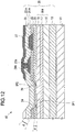
- FIG. 12 is a partial cross-sectional view of a surface emitting laser 10 according to a third embodiment of the present invention.
- the elements of the surface emitting laser 10 according to the third embodiment are substantially identical to those of the surface emitting laser 10 according to the second embodiment except that the pad electrode 29 for threshold current adjustment is not provided according to the third embodiment.
- a description of the configuration and operations of the elements to which the same reference numerals are assigned will be omitted here.
- the threshold current may be adjusted by forming the mixed composition layer 24 by performing the excess pulse application treatment.
- the threshold current adjustment electrode 27 may be buried under the second multilayer film reflector 25.
- FIG. 13 Since two transparent electrode layers are employed, as illustrated in FIG. 13 , the film thickness of the transparent electrodes at the opening increases, and a resulting increase in absorption is of concern.
- a modified example of FIG. 13 may be configured such that the ITO layer, which is a part of the driving transparent electrode 23A in the opening OP2, is removed or absent and the transparent electrode 23 for threshold current adjustment remains as it is.
- the surface emitting laser according to the present invention reduces the threshold current (power consumption) of the surface emitting laser itself and improves the manufacturing yield of the surface emitting lasers.
- the surface emitting laser according to the present invention is advantageous in reducing differences between the threshold currents of a plurality of surface emitting lasers when the surface emitting lasers are arrayed.
- any of the embodiments of the present invention may be applied to a surface emitting laser configured to have an active layer of a quantum well (QW) structure as the active layer 17.
- QW quantum well
- the configuration where the semiconductor structure layer SEM comprises a GaN (gallium nitride) semiconductor has been explained, but the crystal system is not limited thereto. Also, the aforementioned embodiments may be appropriately modified or combined to each other.
- the present invention may be applied not only to a laser, but also to a vertical cavity light emitting device.
Landscapes
- Physics & Mathematics (AREA)
- Condensed Matter Physics & Semiconductors (AREA)
- General Physics & Mathematics (AREA)
- Electromagnetism (AREA)
- Optics & Photonics (AREA)
- Semiconductor Lasers (AREA)
Abstract
Description
- The present invention relates to a vertical cavity light emitting device, such as a vertical cavity surface emitting laser (VCSEL).
- A vertical cavity surface emitting laser is a type of semiconductor laser configured so that light is resonated vertically with respect to a substrate surface and emitted in a vertical direction to the substrate surface. For example,
Japanese Patent Application Laid-Open No. 2011-29607 - A vertical cavity light emitting device, such as a vertical cavity surface emitting laser, has reflecting mirrors that are opposite to each other with a light emitting layer interposed therebetween, and these reflecting mirrors form a resonator or cavity. In a vertical cavity surface emitting laser, for example, a reflecting mirror can be formed by alternately laminating two types of thin films with different refractive indexes.
- To lower the lasing threshold current of a vertical cavity surface emitting laser, it is desirable that a reflecting mirror have high reflection characteristics. It is preferable that the current applied to the vertical cavity surface emitting laser be injected to a light emitting layer without loss.
- However, in the conventional vertical cavity surface emitting laser, an opening of an insulation layer through which a current is injected to a light emitting layer without loss is not adequately addressed.
- The present invention has been made in view of the foregoing problem. It is an object of the present invention to provide a vertical cavity light emitting device that can reduce the threshold current and enhance the manufacturing yield.
- According to one aspect of the present invention, there is provided a vertical cavity light emitting device including:
- a first multilayer film reflector formed on a substrate;
- a semiconductor structure layer that is formed on the first multilayer film reflector and includes a semiconductor layer of a first conductivity type, an active layer, and a semiconductor layer of a second conductivity type which is opposite to the first conductivity type;
- an insulating current confinement layer formed on the semiconductor layer of the second conductivity type;
- a through opening that is formed in the current confinement layer to penetrate the current confinement layer;
- a transparent electrode for covering the through opening and the current confinement layer, the transparent electrode being in contact with the semiconductor layer of the second conductivity type through the through opening;
- a second multilayer film reflector formed on the transparent electrode; and
- a mixed composition layer that is formed so as to be in contact with an edge of the through opening and in which the current confinement layer and the transparent electrode are mixed.
-
-
FIG. 1 is a perspective view schematically illustrating a configuration of a vertical cavity surface emitting laser according to a first embodiment of the present invention; -
FIG. 2 is a partial cross-sectional view schematically illustrating a part of the vertical cavity surface emitting laser along a line XX ofFIG. 1 ; -
FIG. 3 is a partial cross-sectional view schematically illustrating a part of the vertical cavity surface emitting laser encircled by a dashed line Y ofFIG. 2 ; -
FIG. 4 is a top plan view illustrating the configuration of the vertical cavity surface emitting laser according to the first embodiment of the present invention; -
FIG. 5 is a cross-sectional view illustrating a part of the configuration of the vertical cavity surface emitting laser in the middle of manufacturing according to the first embodiment of the present invention; -
FIG. 6 is a cross-sectional view illustrating a part of the configuration of the vertical cavity surface emitting laser in the middle of manufacturing according to the first embodiment of the present invention; -
FIG. 7 includes partial cross-sectional TEM images showing an area near an edge portion of a current confinement layer on a through opening of the surface emitting laser before and after pulse current injection in a test example according to the first embodiment of the present invention; -
FIG. 8 is a graph showing the results of measuring threshold current changes of the completed surface emitting laser in the test example according to the first embodiment of the present invention; -
FIG. 9 is a perspective view illustrating an outer appearance of a vertical cavity surface emitting laser according to a second embodiment of the present invention; -
FIG. 10 is a partial cross-sectional view schematically illustrating a part of the vertical cavity surface emitting laser along a line XX ofFIG. 9 ; -
FIG. 11 is a perspective view illustrating an outer appearance of a vertical cavity surface emitting laser according to a modified example of the second embodiment of the present invention; -
FIG. 12 is a perspective view illustrating an outer appearance of a vertical cavity surface emitting laser according to a third embodiment of the present invention; and -
FIG. 13 is a cross-sectional view schematically illustrating a part of a configuration of a vertical cavity surface emitting laser according to a modified example of the third embodiment of the present invention. - A vertical cavity surface emitting laser (hereinafter also simply referred to as "surface emitting laser"), which is one example of the vertical cavity light emitting device according to the present invention, will now be described with reference to the drawings. In the following description and the accompanying drawings, the substantially same or equivalent parts will be denoted by the same reference numerals.
- The present inventor has focused on an opening portion of a current confinement layer that is an insulation layer. Also, the present inventor has researched and experimented the relationship between a side wall of the opening portion and the lasing threshold current of a surface emitting laser. As a result, the present inventor has found the structure capable of reducing the threshold current and reached the present invention.
-
FIG. 1 is a perspective view schematically illustrating a configuration of asurface emitting laser 10 according to a first embodiment of the present invention. As illustrated inFIG. 1 , thesurface emitting laser 10 includes an emission port EP of a laser beam BM. Thesurface emitting laser 10 has aresonant portion 20 formed on asemiconductor substrate 11. -
FIG. 2 is a partial cross-sectional view schematically illustrating a part of thesurface emitting laser 10 along a line XX ofFIG. 1 . - As illustrated in
FIG. 2 , for example, a light emitting portion of thesurface emitting laser 10 includes theresonant portion 20 formed on theconductive substrate 11 comprising GaN (gallium nitride), theresonant portion 20 including a conductive firstmultilayer film reflector 13; a semiconductor structure layer SEM; an insulating current confinement layer; atransparent electrode 23; a p-contact layer p-Co; and a secondmultilayer film reflector 25. The semiconductor structure layer SEM is constituted by a GaN semiconductor. An n-contact layer n-Co is formed on the surface opposite to the p-contact layer p-Co of thesubstrate 11. A through opening OP1 of the current confinement layer formed directly below thetransparent electrode 23 of the resonant portion 20 (i.e., interface between thetransparent electrode 23 and the semiconductor structure layer SEM) corresponds to the emission port EP of the laser beam BM. - In this embodiment, the first
multilayer film reflector 13 and the secondmultilayer film reflector 25 are each formed as a distributed Bragg reflector (DBR). The semiconductor structure layer SEM is interposed between the firstmultilayer film reflector 13 and the secondmultilayer film reflector 25 so as to define a resonator structure. To achieve desirable conductivity, insulation property, and refractive index, the firstmultilayer film reflector 13 and the secondmultilayer film reflector 25 are formed by properly adjusting, for example, materials, film thicknesses, and the number of pairs of multilayer films. For example, an insulating multilayer film reflector is formed from a dielectric multilayer film. Examples of the thin film materials for a reflector may include oxides of metals, semimetals, etc.; or nitrides, such as AlN, AlGaN, GaN, BN, and SiN. An insulating multilayer film reflector can be obtained by regularly and alternately laminating at least two dielectric thin films with different refractive indexes, such as SiO2/Nb2O5, SiO2/ZrO2, SiO2/AlN, and Al2O3/Nb2O5. -
FIG. 3 is a partial cross-sectional view schematically illustrating a part of thesurface emitting laser 10 encircled by a dashed line Y ofFIG. 2 . - The semiconductor structure layer SEM is formed from layers on the first
multilayer film reflector 13, i.e., an n-type semiconductor layer 15, anactive layer 17 including a quantum well layer, and a p-type semiconductor layer 19, in this order. In this embodiment, each layer of the firstmultilayer film reflector 13 and the semiconductor structure layer SEM has the composition of AlxInyGa1-x-yN (0 ≤ x ≤ 1, 0 ≤ y ≤ 1, 0 ≤ x + y ≤ 1). For example, the structure of the firstmultilayer film reflector 13 is configured such that a low-refractive index semiconductor layer with the composition of AlInN and a high-refractive index semiconductor layer with the composition of GaN are alternately laminated to form a laminated structure of a plurality of pairs of the low-refractive index and high-refractive index semiconductor layers. Also, in this embodiment, theactive layer 17 has a quantum well structure configured such that a well layer (not shown) with the composition of InGaN and a barrier layer (not shown) with the composition of GaN are alternately laminated to form a laminated structure of a plurality of pairs of the well layer and the barrier layer. The n-type semiconductor layer 15 has the composition of GaN and contains Si as an n-type impurity. The p-type semiconductor layer 19 has the composition of GaN and contains Mg, etc. as a p-type impurity. The n-type semiconductor layer 15 and the p-type semiconductor layer 19 are thereby of opposite conductivity types. - Also, in this embodiment, a buffer layer (not shown) is formed between the
substrate 11 and the firstmultilayer film reflector 13. The firstmultilayer film reflector 13 and the semiconductor structure layer SEM are formed using, for example, a metal organic chemical vapor deposition (MOCVD) method. - The insulating
current confinement layer 21 is formed on the p-type semiconductor layer 19 and has the through opening OP1. Thetransparent electrode 23 is formed over thecurrent confinement layer 21 and the p-type semiconductor layer 19 so as to cover the through opening OP1 and to be in contact with the p-type semiconductor layer 19. Thecurrent confinement layer 21 allows a current to be injected from thetransparent electrode 23 to theactive laser 17 via the through opening OP1. Thecurrent confinement layer 21 blocks injection of a current through a portion other than the through opening OP1. -
FIG. 4 is a top plan view illustrating the configuration of thesurface emitting laser 10 viewed from the beam radiation side. - As illustrated in
FIGs. 3 and 4 , amixed composition layer 24 including the composition (or components) of thecurrent confinement layer 21 and the composition (or components) of thetransparent electrode 23 is annularly formed at the position defining thecurrent confinement layer 21, specifically, along the edge of thecurrent confinement layer 21. The area of the annularmixed composition layer 24 is 1% to 20%, preferably 5% or more, the area of the through opening OP1 and can be properly adjusted by changing a below-described tapered angle θ. As the tapered angle θ decreases, the area of themixed composition layer 24 increases. - Examples of the component materials of the
current confinement layer 21 may include: oxides, such as SiO2, Ga2O3, Al2O3, and ZrO2; and nitrides, such as SiN, AlN, and AlGaN. It is preferable to use SiO2 for thecurrent confinement layer 21. The film thickness of thecurrent confinement layer 21 is 5 to 1000 nm, and preferably 10 to 300 nm. - Examples of the component materials of the
transparent electrode 23 may include a conductive metal oxide such as ITO (Indium Tin Oxide), In2O3, IZO (In-doped ZnO), AZO (Al-doped ZnO), GZO (Ga-doped ZnO), ATO (Sb-doped SnO2), FTO (F-doped SnO2), NTO (Nb-doped TiO2), and ZnO. It is preferable to use ITO for thetransparent electrode 23. The film thickness of thetransparent electrode 23 is 3 to 100 nm, and preferably 20 nm or smaller. - As illustrated in
FIG. 4 , the shape of the through opening OP1 is a circle with a diameter of 1 to 15 µm, and preferably 3 to 10 µm, so that a Gaussian beam can be obtained by maintaining the constant distance from the circle edge to the beam center. Thus, a current can be uniformly injected to theactive layer 17, and a light beam can be uniformly confined. The shape of the through opening OP1 may be a non-circular shape, such as an ellipse or polygon, or a shape similar to a circle. - As illustrated in
FIG. 3 , thecurrent confinement layer 21 has a tapered cross-sectional shape where the thickness decreases toward the mixed composition layer 24 (the edge of the through opening OP1). The tapered angle θ of the tapered cross-sectional shape of thecurrent confinement layer 21 preferably exceeds 0 degrees and is equal to or smaller than 45 degrees. - The semiconductor structure layer SEM of the
surface emitting laser 10 was designed in such a manner that the emission wavelength ranged from 400 to 450 nm. The firstmultilayer film reflector 13, which is an electrically-conducting mirror, was designed so as to include forty laminated pairs of GaN/InAlN. The secondmultilayer film reflector 25, which is a dielectric mirror, was designed so as to include eight laminated pairs of Nb2O5/SiO2. - The predetermined semiconductor structure layer SEM was produced using the MOCVD method on a substrate. The SiO2
current confinement layer 21 with a predetermined thickness on the p-GaN semiconductor layer 19 was subjected to etching or liftoff method to remove SiO2 by means of chemical treatment only in the portion where the through opening OP1 (with an outer diameter of 10 µm) was to be formed. - The edge portion of the
current confinement layer 21 formed along the through opening OP1 by the liftoff method specifically has the tapered cross-section ofFIG. 5 with the tapered angle θ. - Thereafter, an ITO transparent electrode with a predetermined thickness was formed by the electron beam deposition method on the
current confinement layer 21 and over the through opening OP1. The p-contact layer p-Co and the secondmultilayer film reflector 25 were also formed, and, as illustrated inFIG. 6 , an incompletesurface emitting laser 10 without themixed composition layer 24 was thus produced. - As illustrated in
FIG. 6 , across the n-contact layer and p-contact layer p-Co of each of the incompletesurface emitting lasers 10, treatment for injecting a pulse current exceeding the normal current for laser light emission (hereinafter referred to as "excess pulse application treatment") was performed. Along the edge of the through opening, themixed composition layer 24 with a diameter of 10 µm and a width of 200 to 400 nm was annularly produced. -
FIG. 7 shows partial cross-sectional TEM images (a) and (b), which show an area near the edge portion of the through opening of the current confinement layer in the surface emitting laser before and after the excess pulse application treatment, respectively. On the right side of each of (a) and (b) ofFIG. 7 , there is shown a partially enlarged image of the interface portion (shown by a dashed line in the left side image) of each of (a) and (b) ofFIG. 7 . - As shown in the cross-sectional TEM images (a) and (b) of
FIG. 7 , when the tapered angle of the edge along the opening of the SiO2 current confinement layer is small, it can be confirmed that the interface between the SiO2 current confinement layer and the transparent electrode ITO is modified or altered by the excess pulse application treatment, and a mixed composition is generated (i.e., the region between the dashed lines in the right side image of (b) ofFIG. 7 ). - The excess pulse application treatment (injected current: 40 to 50 mA) was performed for the
surface emitting laser 10, whereby a composition mixture was caused to complete surface emitting lasers (i.e., devices A, B, C, and D), in order to measure threshold current changes.FIG. 8 is a graph illustrating the results. The vertical axis ofFIG. 8 represents the pulse threshold current (mA), and the horizontal axis ofFIG. 8 represents the current injection period (second) of the excess pulse application treatment. - The foregoing results have revealed that by mixing the compositions of the
current confinement layer 21 and the transparent electrode ITO, which are SiO2 and ITO, respectively, by the excess pulse application treatment for example, to form themixed composition layer 24, the refractive index changes at the opening edge (i.e., mixed composition layer 24), and the threshold current can be further reduced. As illustrated inFIG. 8 , in addition to a decrease in the threshold current, oscillation of the surface emitting lasers (devices C and D), whose pulse laser oscillation was not initially confirmed, has been confirmed to occur after forming themixed composition layer 24. - To decrease the tapered angle of the
current confinement layer 21 to cause composition mixture by means of the excess pulse application treatment (specifically, to appropriately adjust the tapered angle θ), it has been experimentally found preferable to employ the liftoff method to remove the SiO2 layer at the opening. The experimental results have also revealed that a composition mixture of the ITO of thetransparent electrode 23 and SiO2 is noticeable at least at an edge portion near the edge of the through opening where the film thickness of the SiO2 layer of thecurrent confinement layer 21 is 20 nm or lower. - As described above, according to the embodiment, the threshold current can be controlled on the basis of the application time period of the excess pulse application treatment for generating the
mixed composition layer 24. A uniform threshold current can be applied to a plurality of thesurface emitting lasers 10 in a wafer during manufacturing. The embodiment is particularly advantageous for improving the manufacturing yield of arrayed surface emitting lasers. -
FIG. 9 is a perspective view illustrating an outer appearance of onesurface emitting laser 10 according to a second embodiment of the present invention.FIG. 10 is a partial cross-sectional view schematically illustrating a part of thesurface emitting laser 10 along a line XX ofFIG. 9 . - As illustrated in
FIG. 10 , in addition to thecurrent confinement layer 21 and thetransparent electrode 23 of the first embodiment, thesurface emitting laser 10 according to the second embodiment further includes an insulation layer 21A and a driving transparent electrode 23A. Other elements of the second embodiment are substantially identical to those of the first embodiment, and a description of the configuration and operations of the elements to which the same reference numerals are assigned will be omitted here. - The
surface emitting laser 10 according to this embodiment has a thresholdcurrent adjustment electrode 27 connected to thetransparent electrode 23 and apad electrode 29 that connects the thresholdcurrent adjustment electrode 27 to an outside element. Also, thesurface emitting laser 10 according to this embodiment has adrive electrode 27A connected to the driving transparent electrode 23A and adriving pad electrode 29 that connects thedrive electrode 27A to an outside element. When adjusting the threshold current after the pad electrode formation process, the secondmultilayer film reflector 25 on the thresholdcurrent adjustment electrode 27 should be removed, and two pad electrodes should be used to conduct separation between the driving side and the threshold current adjustment side. The threshold currentadjustment pad electrode 29 can be disposed anywhere other than the opening as long as the threshold currentadjustment pad electrode 29 is electrically insulated from thedriving pad electrode 29A on the upper surface of the device. - In this embodiment, the insulation layer 21A has an annular upper-portion opening OP2 disposed in coaxial with the through opening OP1 of the
current confinement layer 21. On the edge of the upper-portion opening OP2, the insulation layer 21A has a tapered cross-sectional shape that tapers toward themixed composition layer 24 above the tapered cross-sectional shape of thecurrent confinement layer 21. - The driving transparent electrode 23A covers the upper-portion opening OP2 of the insulation layer 21A and is in contact with and electrically connected to the
transparent electrode 23. - In this embodiment, a tapered angle φ at the edge of the upper-portion opening OP2 of the insulation layer 21A is greater than the tapered angle θ at the edge of the opening OP1 of the
current confinement layer 21. - The
current confinement layer 21 on the p-type semiconductor layer 19 is formed so that the tapered angle θ is smaller, and a film of thetransparent electrode 23 is formed thereon. Thetransparent electrode 23 is used for threshold current adjustment. Via the thresholdcurrent adjustment electrode 27, an excessive pulse current is injected from thepad electrode 29 to the current confinement layer 21 (i.e., edge portion of the opening thereof) which is in contact with the interface between thetransparent electrode 23 and the p-type semiconductor layer 19. By means of Joule heat, thetransparent electrode 23 and thecurrent confinement layer 21 are mixed to form themixed composition layer 24. - The upper-portion opening OP2 of the insulation layer 21A on the
transparent electrode 23 is formed by, for example, an etching method so that the tapered angle φ is greater, and a film of the driving transparent electrode 23A is formed thereon. The driving transparent electrode 23A is used for driving thesurface emitting laser 10. -
FIG. 11 is a perspective view illustrating an outer appearance of thesurface emitting laser 10A in which sixteen surface emitting lasers according to the second embodiment of the present invention as the light emitting portions are arranged in a 4-by-4 array fashion. -
FIG. 12 is a partial cross-sectional view of asurface emitting laser 10 according to a third embodiment of the present invention. - As illustrated in
FIG. 12 , the elements of thesurface emitting laser 10 according to the third embodiment are substantially identical to those of thesurface emitting laser 10 according to the second embodiment except that thepad electrode 29 for threshold current adjustment is not provided according to the third embodiment. A description of the configuration and operations of the elements to which the same reference numerals are assigned will be omitted here. - After the process of forming the threshold
current adjustment electrode 27 connected to thetransparent electrode 23, which is illustrated inFIG. 12 , the threshold current may be adjusted by forming themixed composition layer 24 by performing the excess pulse application treatment. In this case, the thresholdcurrent adjustment electrode 27 may be buried under the secondmultilayer film reflector 25. - Since two transparent electrode layers are employed, as illustrated in
FIG. 13 , the film thickness of the transparent electrodes at the opening increases, and a resulting increase in absorption is of concern. A modified example ofFIG. 13 may be configured such that the ITO layer, which is a part of the driving transparent electrode 23A in the opening OP2, is removed or absent and thetransparent electrode 23 for threshold current adjustment remains as it is. - As described in the foregoing, the surface emitting laser according to the present invention reduces the threshold current (power consumption) of the surface emitting laser itself and improves the manufacturing yield of the surface emitting lasers. In particular, the surface emitting laser according to the present invention is advantageous in reducing differences between the threshold currents of a plurality of surface emitting lasers when the surface emitting lasers are arrayed.
- Any of the embodiments of the present invention may be applied to a surface emitting laser configured to have an active layer of a quantum well (QW) structure as the
active layer 17. The configuration where the semiconductor structure layer SEM comprises a GaN (gallium nitride) semiconductor has been explained, but the crystal system is not limited thereto. Also, the aforementioned embodiments may be appropriately modified or combined to each other. The present invention may be applied not only to a laser, but also to a vertical cavity light emitting device. - This application is based on a
Japanese Patent Application No. 2015-227165
Claims (9)
- A vertical cavity light emitting device comprising:a first multilayer film reflector formed on a substrate;a semiconductor structure layer that is formed on the first multilayer film reflector and includes a semiconductor layer of a first conductivity type, an active layer, and a semiconductor layer of a second conductivity type which is opposite to the first conductivity type;an insulating current confinement layer formed on the semiconductor layer of the second conductivity type;a through opening that is formed in the current confinement layer to penetrate the current confinement layer;a transparent electrode for covering the through opening and the current confinement layer, the transparent electrode being in contact with the semiconductor layer of the second conductivity type through the through opening;a second multilayer film reflector formed on the transparent electrode; anda mixed composition layer that is formed so as to be in contact with an edge of the through opening and in which the current confinement layer and the transparent electrode are mixed.
- The vertical cavity light emitting device according to claim 1, wherein the mixed composition layer is annularly formed on the semiconductor layer of the second conductivity type.
- The vertical cavity light emitting device according to claim 1 or 2, wherein the current confinement layer has a tapered cross-sectional shape where a thickness thereof decreases towards the mixed composition layer.
- The vertical cavity light emitting device according to claim 3, wherein a tapered angle of the tapered cross-sectional shape of the current confinement layer exceeds 0 degrees and is equal to smaller than 45 degrees.
- The vertical cavity light emitting device according to any one of claims 1 to 4, wherein the current confinement layer comprises SiO2, and the transparent electrode comprises a metal oxide.
- The vertical cavity light emitting device according to any one of claims 1 to 5, wherein a film thickness of the current confinement layer at the through opening adjacent to the mixed composition layer is 20 nm or lower.
- The vertical cavity light emitting device according to any one of claims 1 to 6, further comprising:an insulation layer that has an upper opening disposed in coaxial with the through opening of the current confinement layer and has, at an edge of the upper opening, a tapered cross-sectional shape where a thickness decreases towards the mixed composition layer on a part of a tapered cross-sectional shape of the current confinement layer; anda driving transparent electrode for covering the upper opening, the driving transparent electrode being in contact with the transparent electrode.
- The vertical cavity light emitting device according to claim 7, wherein a tapered angle of the tapered cross-sectional shape of the insulation layer is greater than a tapered angle of the tapered cross-sectional shape of the current confinement layer.
- The vertical cavity light emitting device according to claim 7 or 8, further comprising a pad electrode and a driving pad electrode independently connected to the transparent electrode and the driving transparent electrode, respectively.
Applications Claiming Priority (1)
| Application Number | Priority Date | Filing Date | Title |
|---|---|---|---|
| JP2015227165A JP6700027B2 (en) | 2015-11-20 | 2015-11-20 | Vertical cavity light emitting device |
Publications (2)
| Publication Number | Publication Date |
|---|---|
| EP3171466A1 true EP3171466A1 (en) | 2017-05-24 |
| EP3171466B1 EP3171466B1 (en) | 2018-06-27 |
Family
ID=57326303
Family Applications (1)
| Application Number | Title | Priority Date | Filing Date |
|---|---|---|---|
| EP16199102.1A Active EP3171466B1 (en) | 2015-11-20 | 2016-11-16 | Vertical cavity light emitting device |
Country Status (3)
| Country | Link |
|---|---|
| US (1) | US9972972B2 (en) |
| EP (1) | EP3171466B1 (en) |
| JP (1) | JP6700027B2 (en) |
Families Citing this family (11)
| Publication number | Priority date | Publication date | Assignee | Title |
|---|---|---|---|---|
| JP6135559B2 (en) * | 2014-03-10 | 2017-05-31 | ソニー株式会社 | Semiconductor light emitting device, method for manufacturing semiconductor light emitting device, and semiconductor device |
| KR102654925B1 (en) | 2016-06-21 | 2024-04-05 | 삼성디스플레이 주식회사 | Display apparatus and manufacturing method of the same |
| JP7180984B2 (en) * | 2018-03-01 | 2022-11-30 | 株式会社ニューフレアテクノロジー | Vapor growth method |
| WO2020026573A1 (en) * | 2018-07-31 | 2020-02-06 | ソニー株式会社 | Surface emitting semiconductor laser |
| JP7166871B2 (en) | 2018-10-18 | 2022-11-08 | スタンレー電気株式会社 | Vertical cavity light emitting device |
| JP7190865B2 (en) | 2018-10-18 | 2022-12-16 | スタンレー電気株式会社 | Vertical cavity light emitting device |
| JP7258591B2 (en) | 2019-02-21 | 2023-04-17 | スタンレー電気株式会社 | Vertical cavity light emitting device |
| JP7288360B2 (en) | 2019-07-01 | 2023-06-07 | スタンレー電気株式会社 | Vertical cavity light emitting device |
| DE102022134465B4 (en) * | 2022-01-01 | 2026-05-07 | Canon Kabushiki Kaisha | Semiconductor light emission component, light emission device and distance measuring device |
| CN116505373A (en) * | 2023-03-30 | 2023-07-28 | 厦门市三安集成电路有限公司 | A kind of semiconductor laser and its preparation method |
| WO2025051854A1 (en) * | 2023-09-08 | 2025-03-13 | Ams-Osram International Gmbh | Vcsel device including a current-spreading layer |
Citations (6)
| Publication number | Priority date | Publication date | Assignee | Title |
|---|---|---|---|---|
| US4495514A (en) * | 1981-03-02 | 1985-01-22 | Eastman Kodak Company | Transparent electrode light emitting diode and method of manufacture |
| US20100098127A1 (en) * | 2008-10-22 | 2010-04-22 | Nichia Corporation | Method of manufacturing nitride semiconductor light emitting element and nitride semiconductor light emitting element |
| US20100148202A1 (en) * | 2008-12-12 | 2010-06-17 | Sony Corporation | Semiconductor light-emitting device and method for manufacturing the same |
| JP2011029607A (en) | 2009-06-30 | 2011-02-10 | Nichia Corp | Vertical resonator type surface-emitting laser |
| US20110121337A1 (en) * | 2007-12-19 | 2011-05-26 | Rohm Co., Ltd. | Semiconductor light-emitting device |
| JP2015227165A (en) | 2015-09-16 | 2015-12-17 | テイ・エス テック株式会社 | Vehicle seat |
Family Cites Families (15)
| Publication number | Priority date | Publication date | Assignee | Title |
|---|---|---|---|---|
| JPH10177732A (en) * | 1996-12-16 | 1998-06-30 | Hitachi Ltd | Optical recording / reproducing method, optical recording / reproducing device, semiconductor laser device, and method of manufacturing the same |
| US6185241B1 (en) * | 1998-10-29 | 2001-02-06 | Xerox Corporation | Metal spatial filter to enhance model reflectivity in a vertical cavity surface emitting laser |
| JP4265875B2 (en) * | 2001-05-28 | 2009-05-20 | 日本オプネクスト株式会社 | Manufacturing method of surface emitting semiconductor laser |
| JP3795007B2 (en) * | 2002-11-27 | 2006-07-12 | 松下電器産業株式会社 | Semiconductor light emitting device and manufacturing method thereof |
| JP4437913B2 (en) * | 2003-11-25 | 2010-03-24 | 富士ゼロックス株式会社 | Surface emitting semiconductor laser device and method for manufacturing the same |
| JP4877471B2 (en) * | 2005-10-25 | 2012-02-15 | 富士ゼロックス株式会社 | Manufacturing method of surface emitting semiconductor laser |
| JP2008211164A (en) * | 2007-01-29 | 2008-09-11 | Matsushita Electric Ind Co Ltd | Nitride semiconductor light emitting device and manufacturing method thereof |
| JP2009032716A (en) * | 2007-07-24 | 2009-02-12 | Canon Inc | Surface emitting laser and manufacturing method thereof |
| US8270447B2 (en) * | 2009-01-08 | 2012-09-18 | Furukawa Electric Co., Ltd. | Semiconductor light emitting element and manufacturing method thereof |
| JP2012015139A (en) * | 2010-06-29 | 2012-01-19 | Fuji Xerox Co Ltd | Vertical cavity surface emitting semiconductor laser, vertical cavity surface emitting semiconductor laser device, optical transmission device and information processing apparatus |
| JP2012019041A (en) * | 2010-07-07 | 2012-01-26 | Furukawa Electric Co Ltd:The | Surface emitting laser |
| JP2014053561A (en) * | 2012-09-10 | 2014-03-20 | Canon Inc | Vertical resonator surface-emitting laser |
| JP2015076425A (en) * | 2013-10-07 | 2015-04-20 | 富士ゼロックス株式会社 | Surface-emitting semiconductor laser, surface-emitting semiconductor laser array, surface-emitting semiconductor laser device, optical transmission device, information processing equipment, and method of manufacturing surface-emitting semiconductor laser |
| CN104682194A (en) * | 2014-11-02 | 2015-06-03 | 北京工业大学 | Double-resonance vertical-cavity surface-emitting laser structure for generating terahertz wave and microwave |
| JP6004063B1 (en) * | 2015-09-09 | 2016-10-05 | 富士ゼロックス株式会社 | Manufacturing method of surface emitting semiconductor laser device |
-
2015
- 2015-11-20 JP JP2015227165A patent/JP6700027B2/en active Active
-
2016
- 2016-11-09 US US15/347,267 patent/US9972972B2/en active Active
- 2016-11-16 EP EP16199102.1A patent/EP3171466B1/en active Active
Patent Citations (6)
| Publication number | Priority date | Publication date | Assignee | Title |
|---|---|---|---|---|
| US4495514A (en) * | 1981-03-02 | 1985-01-22 | Eastman Kodak Company | Transparent electrode light emitting diode and method of manufacture |
| US20110121337A1 (en) * | 2007-12-19 | 2011-05-26 | Rohm Co., Ltd. | Semiconductor light-emitting device |
| US20100098127A1 (en) * | 2008-10-22 | 2010-04-22 | Nichia Corporation | Method of manufacturing nitride semiconductor light emitting element and nitride semiconductor light emitting element |
| US20100148202A1 (en) * | 2008-12-12 | 2010-06-17 | Sony Corporation | Semiconductor light-emitting device and method for manufacturing the same |
| JP2011029607A (en) | 2009-06-30 | 2011-02-10 | Nichia Corp | Vertical resonator type surface-emitting laser |
| JP2015227165A (en) | 2015-09-16 | 2015-12-17 | テイ・エス テック株式会社 | Vehicle seat |
Also Published As
| Publication number | Publication date |
|---|---|
| US20170149213A1 (en) | 2017-05-25 |
| JP2017098347A (en) | 2017-06-01 |
| JP6700027B2 (en) | 2020-05-27 |
| US9972972B2 (en) | 2018-05-15 |
| EP3171466B1 (en) | 2018-06-27 |
Similar Documents
| Publication | Publication Date | Title |
|---|---|---|
| EP3171466B1 (en) | Vertical cavity light emitting device | |
| US10381804B2 (en) | Vertical cavity light emitting element | |
| JP6990499B2 (en) | Manufacturing method of vertical resonator type light emitting element and vertical resonance type light emitting element | |
| US10892601B2 (en) | Vertical cavity light-emitting element | |
| US9444223B2 (en) | Surface-emitting semiconductor laser device and method for producing the same | |
| JP6664688B2 (en) | Vertical cavity light emitting device | |
| US12573818B2 (en) | VCSEL with protrusion having inclined side walls formed in p-side semiconductor layer | |
| JP7665086B2 (en) | Vertical cavity light emitting device | |
| US20250047073A1 (en) | Vertical cavity light-emitting element | |
| US12272927B2 (en) | Vertical cavity surface emitting device | |
| JP7453588B2 (en) | Vertical cavity surface emitting laser device | |
| JP7810774B2 (en) | Vertical cavity light emitting device | |
| WO2020026573A1 (en) | Surface emitting semiconductor laser | |
| CN113491045A (en) | Vertical cavity surface light emitting device | |
| EP4012855B1 (en) | Vertical resonator type light emitting element | |
| JP2025008987A (en) | Vertical cavity light emitting device and light emitting device | |
| JP2009238827A (en) | Light-emitting device |
Legal Events
| Date | Code | Title | Description |
|---|---|---|---|
| PUAI | Public reference made under article 153(3) epc to a published international application that has entered the european phase |
Free format text: ORIGINAL CODE: 0009012 |
|
| AK | Designated contracting states |
Kind code of ref document: A1 Designated state(s): AL AT BE BG CH CY CZ DE DK EE ES FI FR GB GR HR HU IE IS IT LI LT LU LV MC MK MT NL NO PL PT RO RS SE SI SK SM TR |
|
| AX | Request for extension of the european patent |
Extension state: BA ME |
|
| 17P | Request for examination filed |
Effective date: 20171115 |
|
| RBV | Designated contracting states (corrected) |
Designated state(s): AL AT BE BG CH CY CZ DE DK EE ES FI FR GB GR HR HU IE IS IT LI LT LU LV MC MK MT NL NO PL PT RO RS SE SI SK SM TR |
|
| GRAP | Despatch of communication of intention to grant a patent |
Free format text: ORIGINAL CODE: EPIDOSNIGR1 |
|
| RIC1 | Information provided on ipc code assigned before grant |
Ipc: H01S 5/343 20060101ALN20171214BHEP Ipc: H01S 5/183 20060101ALI20171214BHEP Ipc: H01S 5/042 20060101AFI20171214BHEP Ipc: H01S 5/00 20060101ALN20171214BHEP |
|
| INTG | Intention to grant announced |
Effective date: 20180115 |
|
| GRAS | Grant fee paid |
Free format text: ORIGINAL CODE: EPIDOSNIGR3 |
|
| GRAA | (expected) grant |
Free format text: ORIGINAL CODE: 0009210 |
|
| AK | Designated contracting states |
Kind code of ref document: B1 Designated state(s): AL AT BE BG CH CY CZ DE DK EE ES FI FR GB GR HR HU IE IS IT LI LT LU LV MC MK MT NL NO PL PT RO RS SE SI SK SM TR |
|
| REG | Reference to a national code |
Ref country code: GB Ref legal event code: FG4D |
|
| REG | Reference to a national code |
Ref country code: AT Ref legal event code: REF Ref document number: 1013131 Country of ref document: AT Kind code of ref document: T Effective date: 20180715 |
|
| REG | Reference to a national code |
Ref country code: IE Ref legal event code: FG4D |
|
| REG | Reference to a national code |
Ref country code: DE Ref legal event code: R096 Ref document number: 602016003838 Country of ref document: DE |
|
| REG | Reference to a national code |
Ref country code: FR Ref legal event code: PLFP Year of fee payment: 3 |
|
| PG25 | Lapsed in a contracting state [announced via postgrant information from national office to epo] |
Ref country code: BG Free format text: LAPSE BECAUSE OF FAILURE TO SUBMIT A TRANSLATION OF THE DESCRIPTION OR TO PAY THE FEE WITHIN THE PRESCRIBED TIME-LIMIT Effective date: 20180927 Ref country code: FI Free format text: LAPSE BECAUSE OF FAILURE TO SUBMIT A TRANSLATION OF THE DESCRIPTION OR TO PAY THE FEE WITHIN THE PRESCRIBED TIME-LIMIT Effective date: 20180627 Ref country code: LT Free format text: LAPSE BECAUSE OF FAILURE TO SUBMIT A TRANSLATION OF THE DESCRIPTION OR TO PAY THE FEE WITHIN THE PRESCRIBED TIME-LIMIT Effective date: 20180627 Ref country code: NO Free format text: LAPSE BECAUSE OF FAILURE TO SUBMIT A TRANSLATION OF THE DESCRIPTION OR TO PAY THE FEE WITHIN THE PRESCRIBED TIME-LIMIT Effective date: 20180927 Ref country code: SE Free format text: LAPSE BECAUSE OF FAILURE TO SUBMIT A TRANSLATION OF THE DESCRIPTION OR TO PAY THE FEE WITHIN THE PRESCRIBED TIME-LIMIT Effective date: 20180627 |
|
| REG | Reference to a national code |
Ref country code: NL Ref legal event code: MP Effective date: 20180627 |
|
| REG | Reference to a national code |
Ref country code: LT Ref legal event code: MG4D |
|
| PG25 | Lapsed in a contracting state [announced via postgrant information from national office to epo] |
Ref country code: LV Free format text: LAPSE BECAUSE OF FAILURE TO SUBMIT A TRANSLATION OF THE DESCRIPTION OR TO PAY THE FEE WITHIN THE PRESCRIBED TIME-LIMIT Effective date: 20180627 Ref country code: RS Free format text: LAPSE BECAUSE OF FAILURE TO SUBMIT A TRANSLATION OF THE DESCRIPTION OR TO PAY THE FEE WITHIN THE PRESCRIBED TIME-LIMIT Effective date: 20180627 Ref country code: GR Free format text: LAPSE BECAUSE OF FAILURE TO SUBMIT A TRANSLATION OF THE DESCRIPTION OR TO PAY THE FEE WITHIN THE PRESCRIBED TIME-LIMIT Effective date: 20180928 Ref country code: HR Free format text: LAPSE BECAUSE OF FAILURE TO SUBMIT A TRANSLATION OF THE DESCRIPTION OR TO PAY THE FEE WITHIN THE PRESCRIBED TIME-LIMIT Effective date: 20180627 |
|
| REG | Reference to a national code |
Ref country code: AT Ref legal event code: MK05 Ref document number: 1013131 Country of ref document: AT Kind code of ref document: T Effective date: 20180627 |
|
| PG25 | Lapsed in a contracting state [announced via postgrant information from national office to epo] |
Ref country code: NL Free format text: LAPSE BECAUSE OF FAILURE TO SUBMIT A TRANSLATION OF THE DESCRIPTION OR TO PAY THE FEE WITHIN THE PRESCRIBED TIME-LIMIT Effective date: 20180627 |
|
| PG25 | Lapsed in a contracting state [announced via postgrant information from national office to epo] |
Ref country code: EE Free format text: LAPSE BECAUSE OF FAILURE TO SUBMIT A TRANSLATION OF THE DESCRIPTION OR TO PAY THE FEE WITHIN THE PRESCRIBED TIME-LIMIT Effective date: 20180627 Ref country code: PL Free format text: LAPSE BECAUSE OF FAILURE TO SUBMIT A TRANSLATION OF THE DESCRIPTION OR TO PAY THE FEE WITHIN THE PRESCRIBED TIME-LIMIT Effective date: 20180627 Ref country code: SK Free format text: LAPSE BECAUSE OF FAILURE TO SUBMIT A TRANSLATION OF THE DESCRIPTION OR TO PAY THE FEE WITHIN THE PRESCRIBED TIME-LIMIT Effective date: 20180627 Ref country code: RO Free format text: LAPSE BECAUSE OF FAILURE TO SUBMIT A TRANSLATION OF THE DESCRIPTION OR TO PAY THE FEE WITHIN THE PRESCRIBED TIME-LIMIT Effective date: 20180627 Ref country code: CZ Free format text: LAPSE BECAUSE OF FAILURE TO SUBMIT A TRANSLATION OF THE DESCRIPTION OR TO PAY THE FEE WITHIN THE PRESCRIBED TIME-LIMIT Effective date: 20180627 Ref country code: IS Free format text: LAPSE BECAUSE OF FAILURE TO SUBMIT A TRANSLATION OF THE DESCRIPTION OR TO PAY THE FEE WITHIN THE PRESCRIBED TIME-LIMIT Effective date: 20181027 Ref country code: AT Free format text: LAPSE BECAUSE OF FAILURE TO SUBMIT A TRANSLATION OF THE DESCRIPTION OR TO PAY THE FEE WITHIN THE PRESCRIBED TIME-LIMIT Effective date: 20180627 |
|
| PG25 | Lapsed in a contracting state [announced via postgrant information from national office to epo] |
Ref country code: SM Free format text: LAPSE BECAUSE OF FAILURE TO SUBMIT A TRANSLATION OF THE DESCRIPTION OR TO PAY THE FEE WITHIN THE PRESCRIBED TIME-LIMIT Effective date: 20180627 Ref country code: ES Free format text: LAPSE BECAUSE OF FAILURE TO SUBMIT A TRANSLATION OF THE DESCRIPTION OR TO PAY THE FEE WITHIN THE PRESCRIBED TIME-LIMIT Effective date: 20180627 Ref country code: IT Free format text: LAPSE BECAUSE OF FAILURE TO SUBMIT A TRANSLATION OF THE DESCRIPTION OR TO PAY THE FEE WITHIN THE PRESCRIBED TIME-LIMIT Effective date: 20180627 |
|
| REG | Reference to a national code |
Ref country code: DE Ref legal event code: R097 Ref document number: 602016003838 Country of ref document: DE |
|
| PLBE | No opposition filed within time limit |
Free format text: ORIGINAL CODE: 0009261 |
|
| STAA | Information on the status of an ep patent application or granted ep patent |
Free format text: STATUS: NO OPPOSITION FILED WITHIN TIME LIMIT |
|
| PG25 | Lapsed in a contracting state [announced via postgrant information from national office to epo] |
Ref country code: DK Free format text: LAPSE BECAUSE OF FAILURE TO SUBMIT A TRANSLATION OF THE DESCRIPTION OR TO PAY THE FEE WITHIN THE PRESCRIBED TIME-LIMIT Effective date: 20180627 |
|
| 26N | No opposition filed |
Effective date: 20190328 |
|
| PG25 | Lapsed in a contracting state [announced via postgrant information from national office to epo] |
Ref country code: MC Free format text: LAPSE BECAUSE OF FAILURE TO SUBMIT A TRANSLATION OF THE DESCRIPTION OR TO PAY THE FEE WITHIN THE PRESCRIBED TIME-LIMIT Effective date: 20180627 Ref country code: LU Free format text: LAPSE BECAUSE OF NON-PAYMENT OF DUE FEES Effective date: 20181116 |
|
| REG | Reference to a national code |
Ref country code: BE Ref legal event code: MM Effective date: 20181130 |
|
| REG | Reference to a national code |
Ref country code: IE Ref legal event code: MM4A |
|
| PG25 | Lapsed in a contracting state [announced via postgrant information from national office to epo] |
Ref country code: SI Free format text: LAPSE BECAUSE OF FAILURE TO SUBMIT A TRANSLATION OF THE DESCRIPTION OR TO PAY THE FEE WITHIN THE PRESCRIBED TIME-LIMIT Effective date: 20180627 |
|
| PG25 | Lapsed in a contracting state [announced via postgrant information from national office to epo] |
Ref country code: IE Free format text: LAPSE BECAUSE OF NON-PAYMENT OF DUE FEES Effective date: 20181116 |
|
| PG25 | Lapsed in a contracting state [announced via postgrant information from national office to epo] |
Ref country code: BE Free format text: LAPSE BECAUSE OF NON-PAYMENT OF DUE FEES Effective date: 20181130 Ref country code: AL Free format text: LAPSE BECAUSE OF FAILURE TO SUBMIT A TRANSLATION OF THE DESCRIPTION OR TO PAY THE FEE WITHIN THE PRESCRIBED TIME-LIMIT Effective date: 20180627 |
|
| PG25 | Lapsed in a contracting state [announced via postgrant information from national office to epo] |
Ref country code: MT Free format text: LAPSE BECAUSE OF NON-PAYMENT OF DUE FEES Effective date: 20181116 |
|
| PG25 | Lapsed in a contracting state [announced via postgrant information from national office to epo] |
Ref country code: TR Free format text: LAPSE BECAUSE OF FAILURE TO SUBMIT A TRANSLATION OF THE DESCRIPTION OR TO PAY THE FEE WITHIN THE PRESCRIBED TIME-LIMIT Effective date: 20180627 |
|
| PG25 | Lapsed in a contracting state [announced via postgrant information from national office to epo] |
Ref country code: PT Free format text: LAPSE BECAUSE OF FAILURE TO SUBMIT A TRANSLATION OF THE DESCRIPTION OR TO PAY THE FEE WITHIN THE PRESCRIBED TIME-LIMIT Effective date: 20180627 |
|
| PG25 | Lapsed in a contracting state [announced via postgrant information from national office to epo] |
Ref country code: HU Free format text: LAPSE BECAUSE OF FAILURE TO SUBMIT A TRANSLATION OF THE DESCRIPTION OR TO PAY THE FEE WITHIN THE PRESCRIBED TIME-LIMIT; INVALID AB INITIO Effective date: 20161116 Ref country code: CY Free format text: LAPSE BECAUSE OF FAILURE TO SUBMIT A TRANSLATION OF THE DESCRIPTION OR TO PAY THE FEE WITHIN THE PRESCRIBED TIME-LIMIT Effective date: 20180627 Ref country code: MK Free format text: LAPSE BECAUSE OF NON-PAYMENT OF DUE FEES Effective date: 20180627 |
|
| REG | Reference to a national code |
Ref country code: CH Ref legal event code: PL |
|
| PG25 | Lapsed in a contracting state [announced via postgrant information from national office to epo] |
Ref country code: LI Free format text: LAPSE BECAUSE OF NON-PAYMENT OF DUE FEES Effective date: 20191130 Ref country code: CH Free format text: LAPSE BECAUSE OF NON-PAYMENT OF DUE FEES Effective date: 20191130 |
|
| PGFP | Annual fee paid to national office [announced via postgrant information from national office to epo] |
Ref country code: GB Payment date: 20241001 Year of fee payment: 9 |
|
| PGFP | Annual fee paid to national office [announced via postgrant information from national office to epo] |
Ref country code: FR Payment date: 20241001 Year of fee payment: 9 |
|
| PGFP | Annual fee paid to national office [announced via postgrant information from national office to epo] |
Ref country code: DE Payment date: 20250930 Year of fee payment: 10 |