EP3171376A1 - Inductor and inductor module - Google Patents
Inductor and inductor module Download PDFInfo
- Publication number
- EP3171376A1 EP3171376A1 EP16172858.9A EP16172858A EP3171376A1 EP 3171376 A1 EP3171376 A1 EP 3171376A1 EP 16172858 A EP16172858 A EP 16172858A EP 3171376 A1 EP3171376 A1 EP 3171376A1
- Authority
- EP
- European Patent Office
- Prior art keywords
- area
- magnetic direction
- inductor
- direction area
- overlapped
- Prior art date
- Legal status (The legal status is an assumption and is not a legal conclusion. Google has not performed a legal analysis and makes no representation as to the accuracy of the status listed.)
- Withdrawn
Links
- 230000001808 coupling effect Effects 0.000 claims abstract description 21
- 230000004907 flux Effects 0.000 claims description 22
- 238000010586 diagram Methods 0.000 description 8
- 230000001419 dependent effect Effects 0.000 description 2
- 238000011161 development Methods 0.000 description 2
- 230000018109 developmental process Effects 0.000 description 2
- 230000000694 effects Effects 0.000 description 2
- 238000000034 method Methods 0.000 description 1
Images



Classifications
-
- H—ELECTRICITY
- H01—ELECTRIC ELEMENTS
- H01F—MAGNETS; INDUCTANCES; TRANSFORMERS; SELECTION OF MATERIALS FOR THEIR MAGNETIC PROPERTIES
- H01F27/00—Details of transformers or inductances, in general
- H01F27/28—Coils; Windings; Conductive connections
-
- H—ELECTRICITY
- H01—ELECTRIC ELEMENTS
- H01F—MAGNETS; INDUCTANCES; TRANSFORMERS; SELECTION OF MATERIALS FOR THEIR MAGNETIC PROPERTIES
- H01F27/00—Details of transformers or inductances, in general
- H01F27/34—Special means for preventing or reducing unwanted electric or magnetic effects, e.g. no-load losses, reactive currents, harmonics, oscillations, leakage fields
-
- H—ELECTRICITY
- H01—ELECTRIC ELEMENTS
- H01F—MAGNETS; INDUCTANCES; TRANSFORMERS; SELECTION OF MATERIALS FOR THEIR MAGNETIC PROPERTIES
- H01F27/00—Details of transformers or inductances, in general
- H01F27/28—Coils; Windings; Conductive connections
- H01F27/2804—Printed windings
-
- H—ELECTRICITY
- H01—ELECTRIC ELEMENTS
- H01F—MAGNETS; INDUCTANCES; TRANSFORMERS; SELECTION OF MATERIALS FOR THEIR MAGNETIC PROPERTIES
- H01F27/00—Details of transformers or inductances, in general
- H01F27/28—Coils; Windings; Conductive connections
- H01F27/29—Terminals; Tapping arrangements for signal inductances
-
- H—ELECTRICITY
- H01—ELECTRIC ELEMENTS
- H01F—MAGNETS; INDUCTANCES; TRANSFORMERS; SELECTION OF MATERIALS FOR THEIR MAGNETIC PROPERTIES
- H01F38/00—Adaptations of transformers or inductances for specific applications or functions
-
- H—ELECTRICITY
- H01—ELECTRIC ELEMENTS
- H01F—MAGNETS; INDUCTANCES; TRANSFORMERS; SELECTION OF MATERIALS FOR THEIR MAGNETIC PROPERTIES
- H01F38/00—Adaptations of transformers or inductances for specific applications or functions
- H01F38/14—Inductive couplings
Definitions
- the present invention is related to an inductor and an inductor module which can have a large overlapped region and a low coupling effect according to the pre-characterizing clause of claims 1 and 11.
- Inductors may have an overlapped area causing coupling effect.
- the coupling effect means that a magnetic field created by an electrical current flowing through an inductor induces an effect on another inductor. Accordingly, if a low coupling effect is desired, the overlapped region should be minimized. However, if the overlapped area is small, the inductor module may occupy a large area.
- the present invention aims at providing an inductor module which has a large overlapped area and low coupling effect.
- the present invention aims at providing an inductor which can provide a large overlapped area and low coupling effect to another inductor.
- the claimed inductor module comprises: a first inductor, comprising a first inductor area; and a second inductor, comprising a second inductor area.
- a first overlapped area of the first inductor area and a second overlapped area of the second inductor area are overlapped.
- the second overlapped area comprises at least one first magnetic direction area and at least one second magnetic direction area.
- a ratio between a size of the first magnetic direction area and a size of the second magnetic direction area is a predetermined ratio such that a coupling effect between the first inductor and the second inductor is lower or equals to a predetermined value.
- the claimed inductor comprising: an inductor area, comprising at least one first magnetic direction area and at least one second magnetic direction area.
- a ratio between a size of the first magnetic direction area and a size of the second magnetic direction area is a predetermined ratio such that a ratio between net magnetic flux caused by the first magnetic direction area and magnetic flux caused by the second magnetic direction is lower or equals to a predetermined threshold.
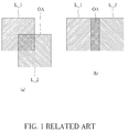
- FIG.1(a), FIG.1(b) are schematic diagrams illustrating a layout of an inductor module for related art.
- the inductor module may comprises more than one inductors, for example, the inductors L_1 and L_2 illustrated in FIG.1(a) and FIG.1(b) .
- the inductors L_1 and L_2 may have an overlapped area OA, which causes coupling effect.
- the coupling effect means that a magnetic field created by an electrical current flowing through an inductor induces an effect on another inductor. Accordingly, if a low coupling effect is desired, the overlapped region should be minimized. However, if the overlapped area is small, the inductor module may occupy a large area.
- FIG.2(a), FIG.2(b), FIG.3(a), FIG.3(b) , FIG.4(a), FIG.4(b) , FIG.5(a), FIG.5(b), FIG.6(a), FIG.6(b) , FIG.7(a), FIG.7 (b), FIG.8(a), FIG. 8 (b) and FIG. 9 are schematic diagrams illustrating an inductor module according to different embodiments of the present application.
- the inductor module 200 comprises a first inductor L_1 and a second inductor L_2.
- the first inductor L_1 comprises a first inductor area IA_1
- the second inductor L_2 comprises a second inductor area IA_2.
- a first overlapped area of the first inductor area IA_1 and a second overlapped area of the second inductor area IA_2 are overlapped.
- the first overlapped area and the second overlapped area mean the overlapped area of the first inductor area IA_1 and the second inductor area IA_2.
- the first overlapped area and the second overlapped area are not marked in the drawings.
- the second overlapped area comprises at least one first magnetic direction area MA_1 and at least one second magnetic direction area MA_2.
- a ratio between a size of the first magnetic direction area MA_1 and a size of the second magnetic direction area MA_2 is a predetermined ratio such that net magnetic flux which the first magnetic direction area MA_1 and the second magnetic direction MA_2 area cause to the first inductor L_1 is lower or equals to a predetermined value. That is, a ratio between a size of the first magnetic direction area MA_1 and a size of the second magnetic direction area MA_2 is a predetermined ratio such that a coupling effect between the first inductor L_1 and the second inductor L_2 is lower or equals to a predetermined value.
- FIG.3(a) illustrates operations for the inductor module 200 illustrated in FIG.2(a) .
- the direction for the magnetic flux for the first magnetic direction area MA_1 which depends on the current I, is out.
- the direction for the magnetic flux for the second magnetic direction area MA_2 is in.
- a ratio between a size of the first magnetic direction area MA_1 and a size of the second magnetic direction area MA_2 is 1. That is, a size of the first magnetic direction area MA_1 and a size of the second magnetic direction area MA_2 are identical. Therefore, the net magnetic flux that the first magnetic direction area MA_1 and the second magnetic direction area MA_2 is substantially 0, which means the coupling effect between the first inductor L_1 and the second inductor L_2 is substantially 0.
- the first magnetic direction area MA_1 and the second magnetic direction area MA_2 form a shape of 8.
- the coil number for the inductor module 200 illustrated in FIG.2(a) is 1.
- the inductor module provided by the present application is not limited to the inductor module 200 illustrated in FIG. 2 (a) .
- the inductor module 210 illustrated in FIG.2(b) has a shape of S, which is different from the structure of the inductor module 200 illustrated in FIG.2(a) .
- the current input terminal CI in FIG.2 (a) and the current input terminal CI in FIG.2(b) have different locations. Also, the coil numbers for the first magnetic direction area MA_1 and the second magnetic direction area MA_2 in in FIG. 2 (a) and the coil numbers for the first magnetic direction area MA_1 and the second magnetic direction area MA_2 in in FIG.2(b) are different.
- FIG.3(b) illustrates the operations for the inductor module 210 illustrated in FIG.2 (b) .
- the direction of the magnetic flux for the first magnetic direction area MA_1 is out.
- the direction for the magnetic flux for the second magnetic direction area MA_2 is in.
- a ratio between a size of the first magnetic direction area MA_1 and a size of the second magnetic direction area MA_2 is 1. That is, a size of the first magnetic direction area MA_1 and a size of the second magnetic direction area MA_2 are identical. Therefore, the net magnetic flux that the first magnetic direction area MA_1 and the second magnetic direction area MA_2 is substantially 0, which means the coupling effect between the first inductor L_1 and the second inductor L_2 is substantially 0.
- the structure of the first inductor L_1 is not limited to the embodiments illustrated in FIG.2(a) and FIG.2(b) .
- the first inductor L_1 in the embodiment of FIG. 2 (a) has a square shape.
- the first inductor L_1 in the embodiment FIG.4 (a) has a shape of 8.
- the second over lapped area of the second inductor L_2 is smaller than the second inductor area IA_2. That is, some part of the second inductor area IA_2 is not overlapped with the first inductor area IA_1.
- the second inductor area IA_2 comprises a plurality of first magnetic direction areas MA_11 and MA_12, and a plurality of second magnetic direction areas MA_21 and MA_22. Additionally, in such embodiments, the magnetic flux caused by the first magnetic direction areas MA_11 and the magnetic flux caused by the second magnetic direction areas MA_22 are neutralized. Similarly, the magnetic flux caused by the first magnetic direction areas MA_12 and the magnetic flux caused by the second magnetic direction areas MA_21 are neutralized.
- the first inductor L_1 in the embodiment of FIG.4(b) comprises a structure the same as the structure for the second inductor L_2 of the embodiment illustrated in FIG. 2 (b) . That is, the coil number for the first inductor L_1 in the embodiment of FIG.4 (b) is more than one.
- the operations for the inductor module illustrated in FIG.4(b) is similar with the inductor module illustrated in FIG.2(b) , thus are omitted for brevity here.
- the first overlapped area L_1 comprises a third overlapped area (ex. the area comprising the first magnetic direction area MA_11 and the second magnetic direction area MA_21 in FIG.4 (a) ) and a fourth overlapped area (ex. the area comprising the first magnetic direction area MA_12 and the second magnetic direction area MA_22 in FIG.4 (a) ) .
- the third overlapped area overlaps with at least one the first magnetic direction area and at least one the second magnetic direction area.
- the fourth overlapped area overlaps with at least one the first magnetic direction area and at least one the second magnetic direction area.
- a ratio between a size of the first magnetic direction area MA_1 and a size of the second magnetic direction area MA_2 is 1.
- such ratio is not limited to 1.
- the following embodiments illustrate such cases .
- some symbols such as the first inductor area IA_1 and the second inductor area IA_2 in the embodiments illustrated in FIG. 5 (a) , FIG. 5 (b) , FIG.6(a), FIG.6(b) , FIG.7(a), FIG.7(b), FIG. 8 (a) and FIG. 8 (b) are not illustrated.
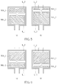
- the first magnetic direction area MA_1 is smaller than the second magnetic direction area MA_2. Also, in the embodiment of FIG.5(b) , the first magnetic direction area MA_1 is much smaller than the second magnetic direction area MA_2. On the opposite, in the embodiment of FIG.6(a) , the first magnetic direction area MA_1 is larger than the second magnetic direction area MA_2. Also, in the embodiment of FIG. 6 (b) , the first magnetic direction area MA_1 is much larger than the second magnetic direction area MA_2.
- the coupling effects for the embodiments illustrated in FIG.5(a) and FIG.6(a) are weaker than the embodiments illustrated in FIG.5(b) and FIG.6(b) since the differences between the a size of the first magnetic direction area MA_1 and a size of the second magnetic direction area MA_2 for the embodiments illustrated in FIG.5(a) and FIG.6(a) are smaller than the differences between the a size of the first magnetic direction area MA_1 and a size of the second magnetic direction area MA_2 for the embodiments illustrated in FIG.5(b) and FIG.6(b) . Accordingly, the coupling effect for the inductor module can be adjusted via adjusting the ratio between a size of the first magnetic direction area MA_1 and a size of the second magnetic direction area MA_2.
- FIG.7(a), FIG.7(b), FIG.8(a) and FIG. 8 (b) illustrate other embodiments that the ratio between a size of the first magnetic direction area MA_1 and a size of the second magnetic direction area MA_2 is a positive rational number other than 1.
- the embodiment illustrated in FIG.7(a) is similar with the embodiment illustrated in FIG.4(a) .
- a size of the first magnetic direction area MA_11 is smaller than a size of the first magnetic direction area MA_12
- a size of the second magnetic direction area MA_21 is smaller than a size of the second magnetic direction area MA_22, in the embodiment of FIG.7 (a) .
- a size of the first magnetic direction area MA_11 is much smaller than a size of the first magnetic direction area MA_12
- a size of the second magnetic direction area MA_21 is much smaller than a size of the second magnetic direction area MA_22, in the embodiment of FIG.7 (b) .
- a size of the first magnetic direction area MA_11 is larger than a size of the first magnetic direction area MA_12, and a size of the second magnetic direction area MA_21 is larger than a size of the second magnetic direction area MA_22, in the embodiment of FIG.8 (a) .
- a size of the first magnetic direction area MA_11 is much larger than a size of the first magnetic direction area MA_12, and a size of the second magnetic direction area MA_21 is much larger than a size of the second magnetic direction area MA_22, in the embodiment of FIG.8(b) .
- the coupling effects for the embodiments illustrated in FIG.7(a) and FIG.7(a) are weaker than the embodiments illustrated in FIG.7(b) and FIG.8(b) since the differences between the sizes of the first magnetic direction areas MA_11, MA_12 and sizes of the second magnetic direction areas MA_21, MA_22 for the embodiments illustrated in FIG. 7 (a) and FIG. 8 (a) are smaller than the differences between the sizes of the first magnetic direction areas MA_11, MA_12 and sizes of the second magnetic direction areas MA_21, MA_22 for the embodiments illustrated in FIG.7(b) and FIG.8(b) . Accordingly, the coupling effect for the inductor module can be adjusted via adjusting the ratio between a size of the first magnetic direction area MA_1 and a size of the second magnetic direction area MA_2.
- the second overlapped area L_2 comprises a current input terminal CI and a current output terminal CO (the locations of CI and CO can be swapped). Sizes of the second magnetic direction areas MA_21, MA_22 which are closer to the current input terminal CI and the current output terminal CO than the first magnetic direction areas MA_11, MA_12 are smaller (in another embodiment, larger) than sizes of the first magnetic direction area MA_11, MA_12.
- the first overlapped area L_1 comprises a third overlapped area (ex. the area comprising the first magnetic direction area MA_11 and the second magnetic direction area MA_21 in FIG. 7 (a) ) and a fourth overlapped area (ex. the area comprising the first magnetic direction area MA_12 and the second magnetic direction area MA_22 in FIG.7 (a) ).
- the third overlapped area overlaps with at least one the first magnetic direction area and at least one the second magnetic direction area.
- the fourth overlapped area overlaps with at least one the first magnetic direction area and at least one the second magnetic direction area.
- the first magnetic direction area overlapping with the third overlapped area (ex. MA_11 in FIG. 7 (a) ) and the second magnetic direction area (ex.MA_21 in FIG.7(a) )overlapping with the third overlapped area have different sizes.
- the coil number for the first magnetic direction area and coil number for the second magnetic direction area are identical.
- either the coil number for the first magnetic direction area MA_1 or the coil number for the second magnetic direction area MA_2 are 1 in FIG.2(a)
- either the coil number for the first magnetic direction area MA_1 or the coil number for the second magnetic direction area MA_2 are 2 in FIG.2(b) .
- the coil number for the first magnetic direction area and coil number for the second magnetic direction area can be different.
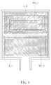
- the coil number for the first magnetic direction area MA_1 is larger than the coil number for the second magnetic direction area MA_2. Accordingly, the first magnetic direction area MA_1 causes a magnetic flux stronger than the magnetic flux caused by the second magnetic direction area MA_2 even if the size for the first magnetic direction area MA_1 and the size for the second magnetic direction area MA_2 are the same. Similarly, the first magnetic direction area MA_1 may cause a magnetic flux the same as the magnetic flux caused by the second magnetic direction area MA_2 even if the size for the first magnetic direction area MA_1 and the size for the second magnetic direction area MA_2 are different, via assigning different coil numbers to the first magnetic direction area MA_1 and the second magnetic direction area MA_2.
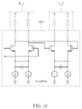
- FIG.10 is a circuit diagram illustrating an exemplary application for the inductor module provided by the present application.
- the inductors L_1, L_2 are applied to an amplifier 1001.
- the inductors L_1, L_2 can have overlapped areas illustrated in above-mentioned embodiments.
- the inductors provided by the present application are not limited to be applied to an amplifier.
- the second inductor L_2 is not limited to be applied with the inductor L_1.
- the second inductor L_2 illustrated in different embodiments can be summarized as: an inductor, comprising: an inductor area, comprising at least one first magnetic direction area and at least one second magnetic direction area.
- a ratio between a size of the first magnetic direction area and a size of the second magnetic direction area is a predetermined ratio such that a ratio between net magnetic flux caused by the first magnetic direction area and magnetic flux caused by the second magnetic direction is lower or equals to a predetermined threshold.
- the inductor module can have overlapped areas and low coupling effect. Accordingly, the issue mentioned in the related art can be resolved. Additionally, the coupling effect between two inductors can be controlled via adjusting the structure of the inductor, which causes the inductor module more applicable. Additionally, an inductor that can adjust an amount of magnetic flux which provides via setting the structure thereof is also provided.
Landscapes
- Engineering & Computer Science (AREA)
- Power Engineering (AREA)
- Coils Or Transformers For Communication (AREA)
Abstract
Description
- The present invention is related to an inductor and an inductor module which can have a large overlapped region and a low coupling effect according to the pre-characterizing clause of
claims - Inductors may have an overlapped area causing coupling effect. The coupling effect means that a magnetic field created by an electrical current flowing through an inductor induces an effect on another inductor. Accordingly, if a low coupling effect is desired, the overlapped region should be minimized. However, if the overlapped area is small, the inductor module may occupy a large area.
- This in mind, the present invention aims at providing an inductor module which has a large overlapped area and low coupling effect.
- This is achieved by an inductor module according to
claim 1. The dependent claims pertain to corresponding further developments and improvements. - Further, the present invention aims at providing an inductor which can provide a large overlapped area and low coupling effect to another inductor.
- This is achieved by a method of managing an inductor according to
claim 11. The dependent claims pertain to corresponding further developments and improvements. - As will be seen more clearly from the detailed description following below, the claimed inductor module comprises: a first inductor, comprising a first inductor area; and a second inductor, comprising a second inductor area. A first overlapped area of the first inductor area and a second overlapped area of the second inductor area are overlapped. The second overlapped area comprises at least one first magnetic direction area and at least one second magnetic direction area. A ratio between a size of the first magnetic direction area and a size of the second magnetic direction area is a predetermined ratio such that a coupling effect between the first inductor and the second inductor is lower or equals to a predetermined value.
- As will be seen more clearly from the detailed description following below, the claimed inductor comprising: an inductor area, comprising at least one first magnetic direction area and at least one second magnetic direction area. A ratio between a size of the first magnetic direction area and a size of the second magnetic direction area is a predetermined ratio such that a ratio between net magnetic flux caused by the first magnetic direction area and magnetic flux caused by the second magnetic direction is lower or equals to a predetermined threshold.
In the following, the invention is further illustrated by way of example, taking reference to the accompanying drawings. Thereof -
FIG.1(a), FIG.1(b) are schematic diagrams illustrating a layout of an inductor module for related art, -
FIG.2(a), FIG.2 (b) are schematic diagrams illustrating an inductor module according to embodiments of the present application, -
FIG. 3 (a) , FIG. 3 (b) are schematic diagrams illustrating the operations for the embodiments illustrated inFIG.2(a) and FIG.2(b) , -
FIG.4(a), FIG.4(b) ,FIG.5(a), FIG.5(b) ,FIG.6(a), FIG.6(b) ,FIG.7(a), FIG.7(b) ,FIG.8(a), FIG. 8 (b) andFIG. 9 are schematic diagrams illustrating an inductor module according to other embodiments of the present application, and -
FIG.10 is a circuit diagram illustrating an exemplary application for the inductor module provided by the present application. -
FIG.1(a), FIG.1(b) are schematic diagrams illustrating a layout of an inductor module for related art. The inductor module may comprises more than one inductors, for example, the inductors L_1 and L_2 illustrated inFIG.1(a) and FIG.1(b) . - The inductors L_1 and L_2 may have an overlapped area OA, which causes coupling effect. The coupling effect means that a magnetic field created by an electrical current flowing through an inductor induces an effect on another inductor. Accordingly, if a low coupling effect is desired, the overlapped region should be minimized. However, if the overlapped area is small, the inductor module may occupy a large area.
-
FIG.2(a), FIG.2(b), FIG.3(a), FIG.3(b) ,FIG.4(a), FIG.4(b) ,FIG.5(a), FIG.5(b), FIG.6(a), FIG.6(b) ,FIG.7(a), FIG.7 (b), FIG.8(a), FIG. 8 (b) andFIG. 9 are schematic diagrams illustrating an inductor module according to different embodiments of the present application. - As illustrated in
FIG.2(a) , theinductor module 200 comprises a first inductor L_1 and a second inductor L_2. The first inductor L_1 comprises a first inductor area IA_1, and the second inductor L_2 comprises a second inductor area IA_2. A first overlapped area of the first inductor area IA_1 and a second overlapped area of the second inductor area IA_2 are overlapped. Please note the first overlapped area and the second overlapped area mean the overlapped area of the first inductor area IA_1 and the second inductor area IA_2. However, for the simplification of drawings, the first overlapped area and the second overlapped area are not marked in the drawings. - Also, the second overlapped area comprises at least one first magnetic direction area MA_1 and at least one second magnetic direction area MA_2. Besides, a ratio between a size of the first magnetic direction area MA_1 and a size of the second magnetic direction area MA_2 is a predetermined ratio such that net magnetic flux which the first magnetic direction area MA_1 and the second magnetic direction MA_2 area cause to the first inductor L_1 is lower or equals to a predetermined value. That is, a ratio between a size of the first magnetic direction area MA_1 and a size of the second magnetic direction area MA_2 is a predetermined ratio such that a coupling effect between the first inductor L_1 and the second inductor L_2 is lower or equals to a predetermined value.
- Please refer to
FIG.3(a) , which illustrates operations for theinductor module 200 illustrated inFIG.2(a) . As illustrated inFIG.3(a) , the direction for the magnetic flux for the first magnetic direction area MA_1, which depends on the current I, is out. Also, the direction for the magnetic flux for the second magnetic direction area MA_2 is in. Besides, a ratio between a size of the first magnetic direction area MA_1 and a size of the second magnetic direction area MA_2 is 1. That is, a size of the first magnetic direction area MA_1 and a size of the second magnetic direction area MA_2 are identical. Therefore, the net magnetic flux that the first magnetic direction area MA_1 and the second magnetic direction area MA_2 is substantially 0, which means the coupling effect between the first inductor L_1 and the second inductor L_2 is substantially 0. - Additionally, in the
inductor module 200 illustrated inFIG.2(a) , the first magnetic direction area MA_1 and the second magnetic direction area MA_2 form a shape of 8. Also, the coil number for theinductor module 200 illustrated inFIG.2(a) is 1. However, the inductor module provided by the present application is not limited to theinductor module 200 illustrated inFIG. 2 (a) . For example, theinductor module 210 illustrated inFIG.2(b) has a shape of S, which is different from the structure of theinductor module 200 illustrated inFIG.2(a) . - For more detail, the current input terminal CI in
FIG.2 (a) and the current input terminal CI inFIG.2(b) have different locations. Also, the coil numbers for the first magnetic direction area MA_1 and the second magnetic direction area MA_2 in inFIG. 2 (a) and the coil numbers for the first magnetic direction area MA_1 and the second magnetic direction area MA_2 in inFIG.2(b) are different. -
FIG.3(b) illustrates the operations for theinductor module 210 illustrated inFIG.2 (b) . As illustrated inFIG. 3 (b) , the direction of the magnetic flux for the first magnetic direction area MA_1 is out. Also, the direction for the magnetic flux for the second magnetic direction area MA_2 is in. Besides, a ratio between a size of the first magnetic direction area MA_1 and a size of the second magnetic direction area MA_2 is 1. That is, a size of the first magnetic direction area MA_1 and a size of the second magnetic direction area MA_2 are identical. Therefore, the net magnetic flux that the first magnetic direction area MA_1 and the second magnetic direction area MA_2 is substantially 0, which means the coupling effect between the first inductor L_1 and the second inductor L_2 is substantially 0. - Furthermore, the structure of the first inductor L_1 is not limited to the embodiments illustrated in
FIG.2(a) and FIG.2(b) . For example, the first inductor L_1 in the embodiment ofFIG. 2 (a) has a square shape. However, the first inductor L_1 in the embodimentFIG.4 (a) has a shape of 8. In such embodiment, the second over lapped area of the second inductor L_2 is smaller than the second inductor area IA_2. That is, some part of the second inductor area IA_2 is not overlapped with the first inductor area IA_1. - Also, in such embodiment, the second inductor area IA_2 comprises a plurality of first magnetic direction areas MA_11 and MA_12, and a plurality of second magnetic direction areas MA_21 and MA_22. Additionally, in such embodiments, the magnetic flux caused by the first magnetic direction areas MA_11 and the magnetic flux caused by the second magnetic direction areas MA_22 are neutralized. Similarly, the magnetic flux caused by the first magnetic direction areas MA_12 and the magnetic flux caused by the second magnetic direction areas MA_21 are neutralized.
- Furthermore, the first inductor L_1 in the embodiment of
FIG.4(b) comprises a structure the same as the structure for the second inductor L_2 of the embodiment illustrated inFIG. 2 (b) . That is, the coil number for the first inductor L_1 in the embodiment ofFIG.4 (b) is more than one. The operations for the inductor module illustrated inFIG.4(b) is similar with the inductor module illustrated inFIG.2(b) , thus are omitted for brevity here. - The embodiments illustrated in
FIG.4(a), FIG.4(b) can be summarized as: the first overlapped area L_1 comprises a third overlapped area (ex. the area comprising the first magnetic direction area MA_11 and the second magnetic direction area MA_21 inFIG.4 (a) ) and a fourth overlapped area (ex. the area comprising the first magnetic direction area MA_12 and the second magnetic direction area MA_22 inFIG.4 (a) ) . The third overlapped area overlaps with at least one the first magnetic direction area and at least one the second magnetic direction area. Also, the fourth overlapped area overlaps with at least one the first magnetic direction area and at least one the second magnetic direction area. - In above-mentioned embodiments, a ratio between a size of the first magnetic direction area MA_1 and a size of the second magnetic direction area MA_2 is 1. However, such ratio is not limited to 1. The following embodiments illustrate such cases . Please note, for the simplification of drawings, some symbols such as the first inductor area IA_1 and the second inductor area IA_2 in the embodiments illustrated in
FIG. 5 (a) , FIG. 5 (b) , FIG.6(a), FIG.6(b) ,FIG.7(a), FIG.7(b), FIG. 8 (a) and FIG. 8 (b) are not illustrated. - In the embodiment of
FIG. 5 (a) , the first magnetic direction area MA_1 is smaller than the second magnetic direction area MA_2. Also, in the embodiment ofFIG.5(b) , the first magnetic direction area MA_1 is much smaller than the second magnetic direction area MA_2. On the opposite, in the embodiment ofFIG.6(a) , the first magnetic direction area MA_1 is larger than the second magnetic direction area MA_2. Also, in the embodiment ofFIG. 6 (b) , the first magnetic direction area MA_1 is much larger than the second magnetic direction area MA_2. - The coupling effects for the embodiments illustrated in
FIG.5(a) and FIG.6(a) are weaker than the embodiments illustrated inFIG.5(b) and FIG.6(b) since the differences between the a size of the first magnetic direction area MA_1 and a size of the second magnetic direction area MA_2 for the embodiments illustrated inFIG.5(a) and FIG.6(a) are smaller than the differences between the a size of the first magnetic direction area MA_1 and a size of the second magnetic direction area MA_2 for the embodiments illustrated inFIG.5(b) and FIG.6(b) . Accordingly, the coupling effect for the inductor module can be adjusted via adjusting the ratio between a size of the first magnetic direction area MA_1 and a size of the second magnetic direction area MA_2. -
FIG.7(a), FIG.7(b), FIG.8(a) and FIG. 8 (b) illustrate other embodiments that the ratio between a size of the first magnetic direction area MA_1 and a size of the second magnetic direction area MA_2 is a positive rational number other than 1. The embodiment illustrated inFIG.7(a) is similar with the embodiment illustrated inFIG.4(a) . However, a size of the first magnetic direction area MA_11 is smaller than a size of the first magnetic direction area MA_12, and a size of the second magnetic direction area MA_21 is smaller than a size of the second magnetic direction area MA_22, in the embodiment ofFIG.7 (a) . Similarly, a size of the first magnetic direction area MA_11 is much smaller than a size of the first magnetic direction area MA_12, and a size of the second magnetic direction area MA_21 is much smaller than a size of the second magnetic direction area MA_22, in the embodiment ofFIG.7 (b) . - On the contrary, a size of the first magnetic direction area MA_11 is larger than a size of the first magnetic direction area MA_12, and a size of the second magnetic direction area MA_21 is larger than a size of the second magnetic direction area MA_22, in the embodiment of
FIG.8 (a) . Similarly, a size of the first magnetic direction area MA_11 is much larger than a size of the first magnetic direction area MA_12, and a size of the second magnetic direction area MA_21 is much larger than a size of the second magnetic direction area MA_22, in the embodiment ofFIG.8(b) . - The coupling effects for the embodiments illustrated in
FIG.7(a) and FIG.7(a) are weaker than the embodiments illustrated inFIG.7(b) and FIG.8(b) since the differences between the sizes of the first magnetic direction areas MA_11, MA_12 and sizes of the second magnetic direction areas MA_21, MA_22 for the embodiments illustrated inFIG. 7 (a) and FIG. 8 (a) are smaller than the differences between the sizes of the first magnetic direction areas MA_11, MA_12 and sizes of the second magnetic direction areas MA_21, MA_22 for the embodiments illustrated inFIG.7(b) and FIG.8(b) . Accordingly, the coupling effect for the inductor module can be adjusted via adjusting the ratio between a size of the first magnetic direction area MA_1 and a size of the second magnetic direction area MA_2. - It will be appreciated that the embodiments illustrated in
FIG.7(a), FIG.7(b), FIG. 8 (a) and FIG. 8 (b) can be summarized as: the second overlapped area L_2 comprises a current input terminal CI and a current output terminal CO (the locations of CI and CO can be swapped). Sizes of the second magnetic direction areas MA_21, MA_22 which are closer to the current input terminal CI and the current output terminal CO than the first magnetic direction areas MA_11, MA_12 are smaller (in another embodiment, larger) than sizes of the first magnetic direction area MA_11, MA_12. - Besides, the embodiments illustrated in
FIG.7(a), FIG.7(b), FIG.8(a) and FIG.8(b) can be summarized as: the first overlapped area L_1 comprises a third overlapped area (ex. the area comprising the first magnetic direction area MA_11 and the second magnetic direction area MA_21 inFIG. 7 (a) ) and a fourth overlapped area (ex. the area comprising the first magnetic direction area MA_12 and the second magnetic direction area MA_22 inFIG.7 (a) ). The third overlapped area overlaps with at least one the first magnetic direction area and at least one the second magnetic direction area. Also, the fourth overlapped area overlaps with at least one the first magnetic direction area and at least one the second magnetic direction area. Additionally, the first magnetic direction area overlapping with the third overlapped area (ex. MA_11 inFIG. 7 (a) ) and the second magnetic direction area (ex.MA_21 inFIG.7(a) )overlapping with the third overlapped area have different sizes. - In above-mentioned embodiments, the coil number for the first magnetic direction area and coil number for the second magnetic direction area are identical. For example, either the coil number for the first magnetic direction area MA_1 or the coil number for the second magnetic direction area MA_2 are 1 in
FIG.2(a) , and either the coil number for the first magnetic direction area MA_1 or the coil number for the second magnetic direction area MA_2 are 2 inFIG.2(b) . However, the coil number for the first magnetic direction area and coil number for the second magnetic direction area can be different. - Please refer to
FIG.9 , the coil number for the first magnetic direction area MA_1 is larger than the coil number for the second magnetic direction area MA_2. Accordingly, the first magnetic direction area MA_1 causes a magnetic flux stronger than the magnetic flux caused by the second magnetic direction area MA_2 even if the size for the first magnetic direction area MA_1 and the size for the second magnetic direction area MA_2 are the same. Similarly, the first magnetic direction area MA_1 may cause a magnetic flux the same as the magnetic flux caused by the second magnetic direction area MA_2 even if the size for the first magnetic direction area MA_1 and the size for the second magnetic direction area MA_2 are different, via assigning different coil numbers to the first magnetic direction area MA_1 and the second magnetic direction area MA_2. -
FIG.10 is a circuit diagram illustrating an exemplary application for the inductor module provided by the present application. As illustrated inFIG.10 , the inductors L_1, L_2 are applied to anamplifier 1001. The inductors L_1, L_2 can have overlapped areas illustrated in above-mentioned embodiments. However, the inductors provided by the present application are not limited to be applied to an amplifier. - Please note, the above-mentioned second inductor L_2 is not limited to be applied with the inductor L_1. The second inductor L_2 illustrated in different embodiments can be summarized as: an inductor, comprising: an inductor area, comprising at least one first magnetic direction area and at least one second magnetic direction area. A ratio between a size of the first magnetic direction area and a size of the second magnetic direction area is a predetermined ratio such that a ratio between net magnetic flux caused by the first magnetic direction area and magnetic flux caused by the second magnetic direction is lower or equals to a predetermined threshold.
- In view of above-mentioned embodiments, the inductor module can have overlapped areas and low coupling effect. Accordingly, the issue mentioned in the related art can be resolved. Additionally, the coupling effect between two inductors can be controlled via adjusting the structure of the inductor, which causes the inductor module more applicable. Additionally, an inductor that can adjust an amount of magnetic flux which provides via setting the structure thereof is also provided.
Claims (15)
- An inductor module, characterized by:a first inductor (L_1), comprising a first inductor area (IA_1); anda second inductor (L_2), comprising a second inductor area (IA_2);wherein a first overlapped area of the first inductor area and a second overlapped area of the second inductor area are overlapped;wherein the second overlapped area comprises at least one first magnetic direction area (MA_1) and at least one second magnetic direction area (MA_2); andwherein a ratio between a size of the first magnetic direction area (MA_1) and a size of the second magnetic direction area (MA_2) is a predetermined ratio such that a coupling effect between the first inductor (L_1) and the second inductor (L_2) is lower or equals to a predetermined value.
- The inductor module of claim 1, characterized in that the predetermined value is 0.
- The inductor module of claim 1, characterized in that the predetermined ratio is 1.
- The inductor module of claim 1, characterized in that the predetermined ratio is a positive rational number other than 1.
- The inductor module of claim 1, characterized in that the first overlapped area comprises a third overlapped area (MA_11, MA_21) and a fourth overlapped area (MA_12, A_22), the third overlapped area (MA_11, MA_21) overlaps with at least one the first magnetic direction area (MA_1) and at least one the second magnetic direction area (MA_2), the fourth overlapped area (MA_12, MA_22) overlaps with at least one the first magnetic direction area (MA_1) and at least one the second magnetic direction area (MA_2).
- The inductor module of claim 5, characterized in that the first magnetic direction area (MA_1) overlapping with the third overlapped area (MA_11, MA_21) and the second magnetic direction area (MA_2) overlapping with the third overlapped area (MA_11, MA_21) have different sizes.
- The inductor module of claim 1, characterized in that the second inductor area (IA_2) is larger than the second overlapped area.
- The inductor module of claim 1, characterized in that the second overlapped area comprises a current input terminal (CI) and a current output terminal (CO), sizes of the second magnetic direction areas (MA_2) which are closer to the current input terminal (CI) and the current output terminal (CO) than the first magnetic direction areas (MA_1) are smaller than sizes of the first magnetic direction area (MA_1).
- The inductor module of claim 1, characterized in that the second overlapped area comprises a current input terminal (CI) and a current output terminal (CO), sizes of the second magnetic direction areas (MA_2) which are closer to the current input terminal (CI) and the current output terminal (CO) than the first magnetic direction areas (MA_1) are larger than sizes of the first magnetic direction area (MA_2).
- The inductor module of claim 1, characterized in that a coil number of the first magnetic direction area (MA_1) is larger than a coil number of the second magnetic direction area (MA_2).
- An inductor, characterized by:an inductor area, comprising at least one first magnetic direction area (MA_1) and at least one second magnetic direction area (MA_2);wherein a ratio between a size of the first magnetic direction area (MA_1) and a size of the second magnetic direction area (MA_2) is a predetermined ratio such that a ratio between net magnetic flux caused by the first magnetic direction area and magnetic flux caused by the second magnetic direction is lower or equals to a predetermined threshold.
- The inductor of claim 11, characterized in that the predetermined ratio is a positive rational number equal to or other than 1.
- The inductor of claim 11, characterized in that a coil number of the first magnetic direction area (MA_1) is larger than a coil number of the second magnetic direction area (MA_2).
- The inductor of claim 11, characterized in that the indictor comprises a current input terminal (CI) and a current output terminal (CO), sizes of the second magnetic direction areas (MA_2) which are closer to the current input terminal (CI) and the current output terminal (CO) than the first magnetic direction areas (MA_1) are smaller than sizes of the first magnetic direction area (MA_1).
- The inductor of claim 11, characterized in that the indictor comprises a current input terminal (CI) and a current output terminal (CO), sizes of the second magnetic direction areas (MA_2) which are closer to the current input terminal (CI) and the current output terminal (CO) than the first magnetic direction areas (MA_1) are larger than sizes of the first magnetic direction area (MA_1).
Applications Claiming Priority (2)
| Application Number | Priority Date | Filing Date | Title |
|---|---|---|---|
| US201562258582P | 2015-11-23 | 2015-11-23 | |
| US15/135,558 US20170148558A1 (en) | 2015-11-23 | 2016-04-22 | Inductor and inductor module |
Publications (1)
| Publication Number | Publication Date |
|---|---|
| EP3171376A1 true EP3171376A1 (en) | 2017-05-24 |
Family
ID=56112859
Family Applications (1)
| Application Number | Title | Priority Date | Filing Date |
|---|---|---|---|
| EP16172858.9A Withdrawn EP3171376A1 (en) | 2015-11-23 | 2016-06-03 | Inductor and inductor module |
Country Status (3)
| Country | Link |
|---|---|
| US (1) | US20170148558A1 (en) |
| EP (1) | EP3171376A1 (en) |
| CN (1) | CN106783094A (en) |
Families Citing this family (6)
| Publication number | Priority date | Publication date | Assignee | Title |
|---|---|---|---|---|
| CN110033920B (en) * | 2018-01-11 | 2021-11-02 | 瑞昱半导体股份有限公司 | Stacked Inductor Device |
| JP2019169527A (en) * | 2018-03-22 | 2019-10-03 | Tdk株式会社 | Coil unit, wireless power transmission device, wireless power reception device, and wireless power transmission system |
| JP2020043178A (en) * | 2018-09-07 | 2020-03-19 | 株式会社東芝 | Transformer and signal transmission system |
| US11495389B2 (en) * | 2020-05-12 | 2022-11-08 | Apple Inc. | Inductor with embedded symmetric resonant circuit |
| CN118830039A (en) * | 2022-03-18 | 2024-10-22 | 华为技术有限公司 | Integrated circuits, chips and terminals |
| CN116403800A (en) * | 2023-06-09 | 2023-07-07 | 麦斯塔微电子(深圳)有限公司 | Inductive device, resonant circuit |
Citations (5)
| Publication number | Priority date | Publication date | Assignee | Title |
|---|---|---|---|---|
| US20090146770A1 (en) * | 2007-12-10 | 2009-06-11 | Industrial Technology Research Institute | Planar-like inductor coupling structure |
| US20120244802A1 (en) * | 2011-03-24 | 2012-09-27 | Lei Feng | On chip inductor |
| US20130049484A1 (en) * | 2010-04-30 | 2013-02-28 | Powermat Technologies Ltd. | System and method for transferring power inductively over an extended region |
| US20140070622A1 (en) * | 2012-09-11 | 2014-03-13 | Qualcomm Incorporated | Wireless power transfer system coil arrangements and method of operation |
| US20150009000A1 (en) * | 2013-07-08 | 2015-01-08 | Samsung Electronics Co., Ltd. | Magnetic field generation apparatus having planar structure |
Family Cites Families (2)
| Publication number | Priority date | Publication date | Assignee | Title |
|---|---|---|---|---|
| JP2011159953A (en) * | 2010-01-05 | 2011-08-18 | Fujitsu Ltd | Electronic circuit and electronic device |
| US9275784B2 (en) * | 2011-09-23 | 2016-03-01 | Rambus Inc. | Electronic circuits using coupled multi-inductors |
-
2016
- 2016-04-22 US US15/135,558 patent/US20170148558A1/en not_active Abandoned
- 2016-06-03 EP EP16172858.9A patent/EP3171376A1/en not_active Withdrawn
- 2016-06-08 CN CN201610405342.0A patent/CN106783094A/en active Pending
Patent Citations (5)
| Publication number | Priority date | Publication date | Assignee | Title |
|---|---|---|---|---|
| US20090146770A1 (en) * | 2007-12-10 | 2009-06-11 | Industrial Technology Research Institute | Planar-like inductor coupling structure |
| US20130049484A1 (en) * | 2010-04-30 | 2013-02-28 | Powermat Technologies Ltd. | System and method for transferring power inductively over an extended region |
| US20120244802A1 (en) * | 2011-03-24 | 2012-09-27 | Lei Feng | On chip inductor |
| US20140070622A1 (en) * | 2012-09-11 | 2014-03-13 | Qualcomm Incorporated | Wireless power transfer system coil arrangements and method of operation |
| US20150009000A1 (en) * | 2013-07-08 | 2015-01-08 | Samsung Electronics Co., Ltd. | Magnetic field generation apparatus having planar structure |
Also Published As
| Publication number | Publication date |
|---|---|
| CN106783094A (en) | 2017-05-31 |
| US20170148558A1 (en) | 2017-05-25 |
Similar Documents
| Publication | Publication Date | Title |
|---|---|---|
| US20170148558A1 (en) | Inductor and inductor module | |
| US9653202B2 (en) | Power converter and device integrating inductors in parallel of the same | |
| US9952064B2 (en) | Transformer position sensor with shorted coil | |
| EP2787515A3 (en) | Inductor gap spacer | |
| SG11201805850SA (en) | Magnetic field generator | |
| US20160093432A1 (en) | Interleaved Transformer/Inductor | |
| RU2674009C1 (en) | Parametric orthogonal-flow transformer with independent magnetic wires | |
| IN2012DN05071A (en) | ||
| EP2736055A1 (en) | Enhanced leakage common mode inductor | |
| KR20140054593A (en) | Apparatus for generating terminating resistance for differential input mode communication and differential input mode communication apparatus | |
| US20150042435A1 (en) | Transformer hybrid | |
| CN110648816A (en) | Inductor module | |
| US10943730B2 (en) | Single-ended inductor | |
| WO2014146647A3 (en) | Magnetic switching element in a magnetic circuit arranged in a defined manner including inductor coil and method for providing electrical energy | |
| CN104578798A (en) | Flyback switching power supply | |
| CN108536040B (en) | Inductor control method and device | |
| JP6939203B2 (en) | Circulating current reduction circuit, transformer unit | |
| CN204578360U (en) | A kind of modular power source of integrated common mode inductance | |
| JP2013214585A (en) | Variable inductor | |
| EP3322063B1 (en) | A multi-channel inverter for a photovoltaic apparatus | |
| CN105740572A (en) | Electronic device | |
| JP3189315U (en) | Biaxial iron core thin transformer configuration | |
| WO2023155167A1 (en) | Input/output module and control system | |
| TWI565160B (en) | Network connector | |
| CN113054886A (en) | Insertion inductor arrangement for multiple parallel drivers |
Legal Events
| Date | Code | Title | Description |
|---|---|---|---|
| PUAI | Public reference made under article 153(3) epc to a published international application that has entered the european phase |
Free format text: ORIGINAL CODE: 0009012 |
|
| AK | Designated contracting states |
Kind code of ref document: A1 Designated state(s): AL AT BE BG CH CY CZ DE DK EE ES FI FR GB GR HR HU IE IS IT LI LT LU LV MC MK MT NL NO PL PT RO RS SE SI SK SM TR |
|
| AX | Request for extension of the european patent |
Extension state: BA ME |
|
| 17P | Request for examination filed |
Effective date: 20170925 |
|
| RBV | Designated contracting states (corrected) |
Designated state(s): AL AT BE BG CH CY CZ DE DK EE ES FI FR GB GR HR HU IE IS IT LI LT LU LV MC MK MT NL NO PL PT RO RS SE SI SK SM TR |
|
| STAA | Information on the status of an ep patent application or granted ep patent |
Free format text: STATUS: THE APPLICATION HAS BEEN WITHDRAWN |
|
| 17Q | First examination report despatched |
Effective date: 20190619 |
|
| 18W | Application withdrawn |
Effective date: 20190704 |