EP3171254A1 - Optical component, touchscreen panel, and display device - Google Patents
Optical component, touchscreen panel, and display device Download PDFInfo
- Publication number
- EP3171254A1 EP3171254A1 EP16020474.9A EP16020474A EP3171254A1 EP 3171254 A1 EP3171254 A1 EP 3171254A1 EP 16020474 A EP16020474 A EP 16020474A EP 3171254 A1 EP3171254 A1 EP 3171254A1
- Authority
- EP
- European Patent Office
- Prior art keywords
- optical component
- phase plate
- resin
- display part
- disposed
- Prior art date
- Legal status (The legal status is an assumption and is not a legal conclusion. Google has not performed a legal analysis and makes no representation as to the accuracy of the status listed.)
- Granted
Links
Images

Classifications
-
- G—PHYSICS
- G02—OPTICS
- G02F—OPTICAL DEVICES OR ARRANGEMENTS FOR THE CONTROL OF LIGHT BY MODIFICATION OF THE OPTICAL PROPERTIES OF THE MEDIA OF THE ELEMENTS INVOLVED THEREIN; NON-LINEAR OPTICS; FREQUENCY-CHANGING OF LIGHT; OPTICAL LOGIC ELEMENTS; OPTICAL ANALOGUE/DIGITAL CONVERTERS
- G02F1/00—Devices or arrangements for the control of the intensity, colour, phase, polarisation or direction of light arriving from an independent light source, e.g. switching, gating or modulating; Non-linear optics
- G02F1/01—Devices or arrangements for the control of the intensity, colour, phase, polarisation or direction of light arriving from an independent light source, e.g. switching, gating or modulating; Non-linear optics for the control of the intensity, phase, polarisation or colour
- G02F1/13—Devices or arrangements for the control of the intensity, colour, phase, polarisation or direction of light arriving from an independent light source, e.g. switching, gating or modulating; Non-linear optics for the control of the intensity, phase, polarisation or colour based on liquid crystals, e.g. single liquid crystal display cells
- G02F1/133—Constructional arrangements; Operation of liquid crystal cells; Circuit arrangements
- G02F1/1333—Constructional arrangements; Manufacturing methods
- G02F1/1335—Structural association of cells with optical devices, e.g. polarisers or reflectors
- G02F1/13363—Birefringent elements, e.g. for optical compensation
-
- G—PHYSICS
- G06—COMPUTING OR CALCULATING; COUNTING
- G06F—ELECTRIC DIGITAL DATA PROCESSING
- G06F3/00—Input arrangements for transferring data to be processed into a form capable of being handled by the computer; Output arrangements for transferring data from processing unit to output unit, e.g. interface arrangements
- G06F3/01—Input arrangements or combined input and output arrangements for interaction between user and computer
- G06F3/03—Arrangements for converting the position or the displacement of a member into a coded form
- G06F3/041—Digitisers, e.g. for touch screens or touch pads, characterised by the transducing means
-
- G—PHYSICS
- G06—COMPUTING OR CALCULATING; COUNTING
- G06F—ELECTRIC DIGITAL DATA PROCESSING
- G06F3/00—Input arrangements for transferring data to be processed into a form capable of being handled by the computer; Output arrangements for transferring data from processing unit to output unit, e.g. interface arrangements
- G06F3/01—Input arrangements or combined input and output arrangements for interaction between user and computer
- G06F3/03—Arrangements for converting the position or the displacement of a member into a coded form
- G06F3/041—Digitisers, e.g. for touch screens or touch pads, characterised by the transducing means
- G06F3/042—Digitisers, e.g. for touch screens or touch pads, characterised by the transducing means by opto-electronic means
- G06F3/0421—Digitisers, e.g. for touch screens or touch pads, characterised by the transducing means by opto-electronic means by interrupting or reflecting a light beam, e.g. optical touch-screen
-
- G—PHYSICS
- G02—OPTICS
- G02B—OPTICAL ELEMENTS, SYSTEMS OR APPARATUS
- G02B5/00—Optical elements other than lenses
- G02B5/30—Polarising elements
- G02B5/3083—Birefringent or phase retarding elements
-
- G—PHYSICS
- G02—OPTICS
- G02F—OPTICAL DEVICES OR ARRANGEMENTS FOR THE CONTROL OF LIGHT BY MODIFICATION OF THE OPTICAL PROPERTIES OF THE MEDIA OF THE ELEMENTS INVOLVED THEREIN; NON-LINEAR OPTICS; FREQUENCY-CHANGING OF LIGHT; OPTICAL LOGIC ELEMENTS; OPTICAL ANALOGUE/DIGITAL CONVERTERS
- G02F2202/00—Materials and properties
- G02F2202/28—Adhesive materials or arrangements
-
- G—PHYSICS
- G06—COMPUTING OR CALCULATING; COUNTING
- G06F—ELECTRIC DIGITAL DATA PROCESSING
- G06F3/00—Input arrangements for transferring data to be processed into a form capable of being handled by the computer; Output arrangements for transferring data from processing unit to output unit, e.g. interface arrangements
- G06F3/01—Input arrangements or combined input and output arrangements for interaction between user and computer
- G06F3/03—Arrangements for converting the position or the displacement of a member into a coded form
- G06F3/041—Digitisers, e.g. for touch screens or touch pads, characterised by the transducing means
- G06F3/0412—Digitisers structurally integrated in a display
Definitions
- the invention relates to optical components, touchscreen panels, and display devices.
- Patent Literature 1 Japanese Patent Application Laid-Open Nos. 06-258634 (Patent Literature 1) and 2012-230390 (Patent Literature 2) disclose display devices that are viewable through polarized sunglasses or the like.
- the display device of Patent Literature 1 includes a liquid crystal display (LCD) panel, a front-side polarizing plate on the front of the LCD panel, and a phase plate on the front of the polarizing plate.
- the phase plate is oriented such that its optical axis forms an angle of approximately 35 ⁇ to 55 ⁇ with the absorption axis of the front-side polarizing plate.
- the phase plate is configured to have a retardation in a range of approximately 4,000 nm or larger.
- Linearly polarized light emitted from the front-side polarizing plate travels through the phase plate to be converted into elliptically polarized light.
- the display device is viewable from any direction through polarized sunglasses or the like, without suffering from uneven coloring in the display face.
- the display device of Patent Literature 2 includes an LCD panel, a polymer film, and a polarizing plate disposed therebetween.
- the LCD panel has white light emitting diodes serving as a backlight source.
- the polymer film has retardation in the range of 3,000 nm to 30,000 nm.
- the polymer film is oriented such that its slow axis forms an angle of approximately 45 ⁇ with the absorption axis of the polarizing plate.
- the white light emitting diodes exhibit an emission spectrum of a similar shape to the envelope curve of the spectrum of transmitted light traveling through the polymer film. This configuration aims to improve visibility of the display device when viewed through polarized sunglasses or the like.
- Some display devices include resin panels serving as cover panels or other components.
- the inventor conceived of using resin panels that are molded without controlling their birefringent properties.
- Such resin panels may be fabricated by molding resin without controlling birefringent properties.
- partial birefringence may occur due to the molecular orientations and/or photoelasticity, resulting from material characteristics during the molding process, resin flows during the molding process, and residual stress generated during the molding process, and/or other factors.
- Resin panels may also be fabricated by an extruding process or a stretching process, which may also cause birefringence.
- the conventional display devices described in Patent Literature 1 and Patent Literature 2 referenced above include no resin panels fabricated without controlling phase differences. Accordingly, no considerations have previously been given regarding how to improve display visibility of display devices equipped with such an uncontrolled resin panel when viewed through polarized sunglasses or the like.
- the invention has been conceived in view of the above circumstances to provide an optical component capable of improving display visibility of a display part allowing that the optical component includes a resin part that is uncontrolled with respect to phase difference.
- the invention also provides a touchscreen panel and a display device including the optical component.
- an optical component that can be disposed on an emitting direction side of a display part capable of emitting linearly polarized light.
- the optical component includes a resin part and a phase plate or wave plate.
- the resin part has translucency and is uncontrolled in terms of phase difference.
- the phase plate or wave plate is configured to be disposed between the display part and the resin part.
- the phase plate has three to five times as large retardation as the resin part.
- the optical component of this aspect is disposed, in use, on the emitting direction side of the display part.
- the phase plate has three to five times as large retardation as the resin part, the optical component can suppress the possibility of occurrence of iridescent unevenness and blackout in displayed images of the display part when viewed through a polarizing plate (such as polarized sunglasses or a panel of electronic equipment) and the optical component. Therefore, the invention can improve visibility of displayed images of the display part.
- the retardation of the phase plate may be at least 3,000 nm.
- the retardation of the phase plate may be at least 5,000 nm.
- the retardation of the phase plate may be at least 10,000 nm.
- the phase plate may be oriented, in use, such that an optic axis of the phase plate forms an angle of approximately 45 degrees with a polarization axis of the linearly polarized light emitted from a display part with which the optical component is intended to be used.
- a touchscreen panel of the invention includes the optical component of any of the above aspects and a sensor capable of detecting an approach of a detection target.
- the sensor may be disposed, in use, between the phase plate of the optical component and a display part with which the optical component is intended to be used, or it may be disposed between the resin part of the optical component and the phase plate of the optical component.
- a display device of the invention includes a display part capable of emitting linearly polarized light and the optical component of any of the above aspects.
- the optical component may be disposed on the emitting direction side of the display part.
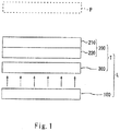
- a display device L according to an embodiment of the invention will be described referring to Fig. 1 .
- the display device L illustrated in Fig. 1 includes a display part 100 and a touchscreen panel T. These constituents of the display device L will be described below in detail.
- the display part 100 can emit linearly polarized light.
- the display part 100 may be an LCD panel, an organic light-emitting diode (OLED) device, or the like.
- the LCD panel may be of a simple matrix driving type or of an active matrix driving type such as a thin-film transistor (TFT) type.
- TFT thin-film transistor
- the touchscreen panel T includes an optical component 200 and a sensor 300.
- the optical component 200 is disposed with spacing from the display part 100, on the side of the emitting direction (direction of arrows illustrated) of linearly polarized light emitted from the display part 100.
- the optical component 200 includes a resin part 210 and a phase plate 220.
- the resin part 210 is of a resin material that is uncontrolled in terms of phase difference.
- it may be a molded resin article that is uncontrolled in terms of phase difference, an extruded plate of resin material (e.g. polycarbonate (PC) resin, PMMA resin, and the like), or a stretched film of resin material (e.g., polyethylene terephthalate, PC, and the like).
- resin molded articles if molded without controlling birefringence, may partially have birefringence due to the molecular orientation and/or photoelasticity, resulting from material characteristics during the molding process, resin flows during the molding process, residual stress generated during the molding process, and/or other factors.
- extruded plates may have birefringence due to the extruding process of resin material.
- Stretched films may have birefringence due to the stretching process of resin material.
- the resin part 210 may become unintentionally birefringent and uncontrolled in terms of phase difference.
- the phase plate 220 is fixed to the rear face of the resin part 210 in the emitting direction so as to be positioned between the resin part 210 and the display part 100.
- the phase plate 220 has three to five times as large retardation as the resin part 210.
- the retardation of the phase plate 220 is set at 3,000 nm or larger. More preferably, the retardation of the phase plate 220 is 5,000 nm or larger, and still more preferably 10,000 nm or larger. This is because, with increasing retardation of the phase plate 220, the light that has traveled through the phase plate 220 contains more wavelengths in which circularly polarized light, elliptically polarized light, and linearly polarized light exist throughout the visible spectrum.
- the phase plate 220 is oriented such that the optic axis (slow axis) of the phase plate 220 forms an angle of approximately 45 ⁇ with the polarization axis of linearly polarized light emitted from the display part 100.
- the sensor 300 is a sensor of the touchscreen panel T and can detect a detection target (a finger or a stylus pen) approaching the display device L.
- the sensor 300 is optically isotropic.
- the sensor 300 is disposed between the display part 100 and the phase plate 220.
- the inventor performed the following experiments in the process of inventing the above display device L.
- the inventor viewed the respective display devices for the first to fourth experimental examples through a polarizing plate P to check if iridescent unevenness and/or blackout occur to displayed images of the display devices.
- the polarizing plate P may be polarized sunglasses, a panel of electronic equipment (a touchscreen panel, a car navigation device, a display device (e.g. an indicator of an automobile), or the like.
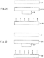
- the display device of the first experimental example as illustrated in Fig. 2A includes a display part 100, and a resin part 210 disposed so as to face the emitting direction side of the display part 100.
- the display device of the second experimental example as illustrated in Fig. 2B includes a display part 100, a resin part 210 on the emitting direction side of the display part 100 with a space therebetween, and a quarter-wave plate 10 on the front of the resin part 210 in the emitting direction.
- the display device of the third experimental example as illustrated in Fig. 2C includes a display part 100, a resin part 210 on the emitting direction side of the display part 100 with a space therebetween, and a quarter-wave plate 10 on the rear of the resin part 210 in the emitting direction.
- Each quarter-wave plate 10 in the second and third experimental examples has a smaller outer face than that of the display part 100.
- the quarter-wave plate 10 has a retardation of 140 nm.
- the display device of the fourth experimental example as illustrated in Fig. 2D includes a display part 100, a resin part 210 disposed on an emitting direction side of the display part 100 with a space therebetween, and a phase plate 220' on the rear face of the resin part 210 in the emitting direction.
- the phase plate 220' has the same configuration as the phase plate 220, only different in that the phase plate 220' has a smaller outer face than that of the display part 100.
- linearly polarized light emitted from the display part 100 directly enters the resin part 210 that is not controlled in terms of phase difference.
- the light changes in polarization state when travelling through the resin part 210.
- iridescent unevenness and/or partial blackout occurred to displayed images of the display device, in any of the cases where the polarization direction of the linearly polarized light of the display part 100 and the polarization direction of the polarizing plate P are (1) substantially parallel to each other, (2) substantially perpendicular to each other, and (3) at an angle to each other that is not parallel or perpendicular.
- linearly polarized light emitted from the display part 100 directly enters the resin part 210 that is not controlled in terms of phase difference.
- the light changes in polarization state when travelling through the resin part 210.
- the changed light then travels through the quarter-wave plate 10 in the superimposed area of the resin part 210 and the quarter-wave plate 10.
- iridescent unevenness and/or partial blackout occurred to displayed images in the superimposed area of the display device, in any of the cases where the polarization direction of the linearly polarized light of the display part 100 and the polarization direction of the polarizing plate P are (1) substantially parallel to each other, (2) substantially perpendicular to each other, and (3) at an angle to each other that is not parallel or perpendicular.
- linearly polarized light emitted from the display part 100 travels through the quarter-wave plate 10 in the superimposed area of the resin part 210 and the quarter-wave plate 10 and then travels through the resin part 210 that is not controlled in terms of phase difference.
- the linearly polarized light traveling through the quarter-wave plate 10 is converted into elliptically polarized light and then changes in polarization state when travelling through the resin part 210.
- iridescent unevenness and/or partial blackout occurred to displayed images in the superimposed area of the display device, in any of the cases where the polarization direction of the linearly polarized light of the display part 100 and the polarization direction of the polarizing plate P are (1) substantially parallel to each other, (2) substantially perpendicular to each other, and (3) at an angle to each other that is not parallel or perpendicular.
- linearly polarized light emitted from the display part 100 travels through the phase plate 220' in the superimposed area of the resin part 210 and the phase plate 220' and then travels through the resin part 210 that is not controlled in terms of phase difference.
- the linearly polarized light traveling through the phase plate 220' is converted into light that contains more wavelengths in which circularly polarized light, elliptically polarized light, and linearly polarized light exist throughout the visible spectrum.
- the light then travels through the resin part 210 and may change in polarization state, but the outgoing light has a wide variety of polarization states throughout the visible spectrum.
- iridescent unevenness and/or blackout did NOT occur to displayed images in the superimposed area of the display device, in any of the cases where the polarization direction of the linearly polarized light of the display part 100 and the polarization direction of the polarizing plate P are (1) substantially parallel to each other, (2) substantially perpendicular to each other, and (3) at an angle to each other that is not parallel or perpendicular.
- the display device L although including the resin part 210 that is not controlled in terms of phase difference, is able to suppress occurrence of iridescent unevenness and blackout in displayed images of the display part 100 when viewed through the polarizing plate P.
- the display device L can thus improve visibility of displayed images of the display device L.
- the linearly polarized light emitted from the display part 100 travels through the phase plate 220 to be converted into light that contains many wavelengths in which circularly polarized light, elliptically polarized light, and linearly polarized light exist throughout the visible spectrum.
- the light then travels through the resin part 210 and may change in polarization state, but the outgoing light has a wide variety of polarization states (i.e.
- the display device L when the display device L is viewed through the polarizing plate P, the displayed images are viewed with color tones close to the colors as going out from the display part 100 because of the suppressed occurrences of iridescent unevenness and/or blackout in the displayed images of the display part 100.
- Larger retardation of the phase plate 220 is preferable because light of a larger variation of wavelengths travels through the polarizing plate P and can be viewed in color tones closer to the light source color of the display part 100.
- the display device L can suppress occurrences of iridescent unevenness and blackout in displayed images of the display device, in any of the cases where the polarization direction of the linearly polarized light of the display part 100 and the polarization direction of the polarizing plate P are (1) substantially parallel to each other, (2) substantially perpendicular to each other, and (3) at an angle to each other that is not parallel or perpendicular.
- the phase plate 220 has retardation of 3,000 nm or larger, certain variation in phase difference within the phase plate 220 would not cause coloring that would be recognizable by human eyes.
- the light traveling through the phase plate 220 is seen in colors similar to the linearly polarized light emitted from the display part 100.
- the display device L, the touchscreen panel T, and the optical component 200 described above are not limited to the above embodiment but may be modified in any manner within the scope of the claims. Specific modifications will be described below in detail.
- the optical component of the invention may be any optical component being adapted to be disposed on an emitting direction side of a display part capable of emitting linearly polarized light, and including a resin part having translucency and being uncontrolled with respect to phase difference; and a phase plate being configured to be disposed between the display part and the resin part and having three to five times as large a retardation as the resin part.
- the resin part and the phase plate described above may be spaced apart from each other. Further, the above phase plate may be fixed to a sensor or a display part so as to be positioned on the emitting direction side of the display part.
- the display device of the invention may be any display device including a display part, capable of emitting linearly polarized light, and an optical component of the above embodiment or the above modifications which can be disposed on the emitting direction side of the display part.
- any optically isotropic member e.g., a sensor of a touchscreen panel, optically clear adhesive (OCA), a triacetyl cellulose (TAC) film, or a cycloolefin polymer (COP) film, and the like.
- OCA optically clear adhesive
- TAC triacetyl cellulose
- COP cycloolefin polymer
- the display part of the invention includes a display part main body and a polarizing plate, and the polarizing plate may be disposed on the light emitting direction side of the display part main body and may convert the light into linearly polarized light.
- the display part of the invention is not limited to one including a display part main body adapted to emit linearly polarized light.
- the invention allows for the touchscreen panel and the display part as separate components.
- the display device L, the touchscreen panel T, and the optical component 200 of the above embodiment are described above by way of example only and may comprise any materials, shapes, dimensions, numbers, arrangements, and other configurations if they can perform similar functions.
- the configurations of the embodiment and the modifications described above may be combined in any possible manner.
Landscapes
- Physics & Mathematics (AREA)
- Engineering & Computer Science (AREA)
- Theoretical Computer Science (AREA)
- General Engineering & Computer Science (AREA)
- General Physics & Mathematics (AREA)
- Nonlinear Science (AREA)
- Human Computer Interaction (AREA)
- Optics & Photonics (AREA)
- Crystallography & Structural Chemistry (AREA)
- Chemical & Material Sciences (AREA)
- Mathematical Physics (AREA)
- Liquid Crystal (AREA)
- Polarising Elements (AREA)
- Devices For Indicating Variable Information By Combining Individual Elements (AREA)
- Electroluminescent Light Sources (AREA)
Abstract
Description
- The invention relates to optical components, touchscreen panels, and display devices.
- Japanese Patent Application Laid-Open Nos.
06-258634 2012-230390 Patent Literature 1 includes a liquid crystal display (LCD) panel, a front-side polarizing plate on the front of the LCD panel, and a phase plate on the front of the polarizing plate. The phase plate is oriented such that its optical axis forms an angle of approximately 35□ to 55□ with the absorption axis of the front-side polarizing plate. The phase plate is configured to have a retardation in a range of approximately 4,000 nm or larger. Linearly polarized light emitted from the front-side polarizing plate travels through the phase plate to be converted into elliptically polarized light. Hence, the display device is viewable from any direction through polarized sunglasses or the like, without suffering from uneven coloring in the display face. - The display device of Patent Literature 2 includes an LCD panel, a polymer film, and a polarizing plate disposed therebetween. The LCD panel has white light emitting diodes serving as a backlight source. The polymer film has retardation in the range of 3,000 nm to 30,000 nm. The polymer film is oriented such that its slow axis forms an angle of approximately 45□ with the absorption axis of the polarizing plate. The white light emitting diodes exhibit an emission spectrum of a similar shape to the envelope curve of the spectrum of transmitted light traveling through the polymer film. This configuration aims to improve visibility of the display device when viewed through polarized sunglasses or the like.
- Some display devices include resin panels serving as cover panels or other components. The inventor conceived of using resin panels that are molded without controlling their birefringent properties. Such resin panels may be fabricated by molding resin without controlling birefringent properties. In this case, partial birefringence may occur due to the molecular orientations and/or photoelasticity, resulting from material characteristics during the molding process, resin flows during the molding process, and residual stress generated during the molding process, and/or other factors. Resin panels may also be fabricated by an extruding process or a stretching process, which may also cause birefringence. It should be noted that the conventional display devices described in
Patent Literature 1 and Patent Literature 2 referenced above include no resin panels fabricated without controlling phase differences. Accordingly, no considerations have previously been given regarding how to improve display visibility of display devices equipped with such an uncontrolled resin panel when viewed through polarized sunglasses or the like. - The invention has been conceived in view of the above circumstances to provide an optical component capable of improving display visibility of a display part allowing that the optical component includes a resin part that is uncontrolled with respect to phase difference. The invention also provides a touchscreen panel and a display device including the optical component.
- In an aspect of the invention, an optical component is provided that can be disposed on an emitting direction side of a display part capable of emitting linearly polarized light. The optical component includes a resin part and a phase plate or wave plate. The resin part has translucency and is uncontrolled in terms of phase difference. The phase plate or wave plate is configured to be disposed between the display part and the resin part. The phase plate has three to five times as large retardation as the resin part.
- The optical component of this aspect is disposed, in use, on the emitting direction side of the display part. As the phase plate has three to five times as large retardation as the resin part, the optical component can suppress the possibility of occurrence of iridescent unevenness and blackout in displayed images of the display part when viewed through a polarizing plate (such as polarized sunglasses or a panel of electronic equipment) and the optical component. Therefore, the invention can improve visibility of displayed images of the display part.
- The retardation of the phase plate may be at least 3,000 nm. The retardation of the phase plate may be at least 5,000 nm. The retardation of the phase plate may be at least 10,000 nm. The phase plate may be oriented, in use, such that an optic axis of the phase plate forms an angle of approximately 45 degrees with a polarization axis of the linearly polarized light emitted from a display part with which the optical component is intended to be used.
- A touchscreen panel of the invention includes the optical component of any of the above aspects and a sensor capable of detecting an approach of a detection target. The sensor may be disposed, in use, between the phase plate of the optical component and a display part with which the optical component is intended to be used, or it may be disposed between the resin part of the optical component and the phase plate of the optical component.
- A display device of the invention includes a display part capable of emitting linearly polarized light and the optical component of any of the above aspects. The optical component may be disposed on the emitting direction side of the display part.
- The invention will now be described by way of example only and without limitation by reference to the drawings, in which:
-
Fig. 1 is an explanatory diagram illustrating a relative positioning of constituents of a display device according to an embodiment of the invention with respect to a polarizing plate; -
Fig. 2A is an explanatory diagram illustrating a relative positioning of constituents of a display device in the first experimental example with respect to a polarizing plate; -
Fig. 2B is an explanatory diagram illustrating a relative positioning of constituents of a display device in the second experimental example with respect to a polarizing plate; -
Fig. 2C is an explanatory diagram illustrating a relative positioning of constituents of a display device in the third experimental example with respect to a polarizing plate; and -
Fig. 2D is an explanatory diagram illustrating a relative positioning of constituents of a display device in the fourth experimental example with respect to a polarizing plate. - A display device L according to an embodiment of the invention will be described referring to
Fig. 1 . The display device L illustrated inFig. 1 includes adisplay part 100 and a touchscreen panel T. These constituents of the display device L will be described below in detail. - As illustrated in
Fig. 1 , thedisplay part 100 can emit linearly polarized light. For example, thedisplay part 100 may be an LCD panel, an organic light-emitting diode (OLED) device, or the like. The LCD panel may be of a simple matrix driving type or of an active matrix driving type such as a thin-film transistor (TFT) type. - The touchscreen panel T includes an
optical component 200 and asensor 300. Theoptical component 200 is disposed with spacing from thedisplay part 100, on the side of the emitting direction (direction of arrows illustrated) of linearly polarized light emitted from thedisplay part 100. Theoptical component 200 includes aresin part 210 and aphase plate 220. Theresin part 210 is of a resin material that is uncontrolled in terms of phase difference. For example, it may be a molded resin article that is uncontrolled in terms of phase difference, an extruded plate of resin material (e.g. polycarbonate (PC) resin, PMMA resin, and the like), or a stretched film of resin material (e.g., polyethylene terephthalate, PC, and the like). Generally speaking, resin molded articles, if molded without controlling birefringence, may partially have birefringence due to the molecular orientation and/or photoelasticity, resulting from material characteristics during the molding process, resin flows during the molding process, residual stress generated during the molding process, and/or other factors. Also, extruded plates may have birefringence due to the extruding process of resin material. Stretched films may have birefringence due to the stretching process of resin material. For any of the above reasons, theresin part 210 may become unintentionally birefringent and uncontrolled in terms of phase difference. - The
phase plate 220 is fixed to the rear face of theresin part 210 in the emitting direction so as to be positioned between theresin part 210 and thedisplay part 100. Thephase plate 220 has three to five times as large retardation as theresin part 210. The retardation of thephase plate 220 is set at 3,000 nm or larger. More preferably, the retardation of thephase plate 220 is 5,000 nm or larger, and still more preferably 10,000 nm or larger. This is because, with increasing retardation of thephase plate 220, the light that has traveled through thephase plate 220 contains more wavelengths in which circularly polarized light, elliptically polarized light, and linearly polarized light exist throughout the visible spectrum. If this traveled light changes in polarization state when travelling through theresin part 210, the outgoing light has a wide variety of polarization states throughout the visible spectrum. Thephase plate 220 is oriented such that the optic axis (slow axis) of thephase plate 220 forms an angle of approximately 45□ with the polarization axis of linearly polarized light emitted from thedisplay part 100. - The
sensor 300 is a sensor of the touchscreen panel T and can detect a detection target (a finger or a stylus pen) approaching the display device L. Thesensor 300 is optically isotropic. Thesensor 300 is disposed between thedisplay part 100 and thephase plate 220. - The inventor performed the following experiments in the process of inventing the above display device L. In these experiments, the inventor viewed the respective display devices for the first to fourth experimental examples through a polarizing plate P to check if iridescent unevenness and/or blackout occur to displayed images of the display devices. It should be appreciated that the polarizing plate P may be polarized sunglasses, a panel of electronic equipment (a touchscreen panel, a car navigation device, a display device (e.g. an indicator of an automobile), or the like.
- The display device of the first experimental example as illustrated in
Fig. 2A includes adisplay part 100, and aresin part 210 disposed so as to face the emitting direction side of thedisplay part 100. The display device of the second experimental example as illustrated inFig. 2B includes adisplay part 100, aresin part 210 on the emitting direction side of thedisplay part 100 with a space therebetween, and a quarter-wave plate 10 on the front of theresin part 210 in the emitting direction. The display device of the third experimental example as illustrated inFig. 2C includes adisplay part 100, aresin part 210 on the emitting direction side of thedisplay part 100 with a space therebetween, and a quarter-wave plate 10 on the rear of theresin part 210 in the emitting direction. Each quarter-wave plate 10 in the second and third experimental examples has a smaller outer face than that of thedisplay part 100. The quarter-wave plate 10 has a retardation of 140 nm. The display device of the fourth experimental example as illustrated inFig. 2D includes adisplay part 100, aresin part 210 disposed on an emitting direction side of thedisplay part 100 with a space therebetween, and a phase plate 220' on the rear face of theresin part 210 in the emitting direction. The phase plate 220' has the same configuration as thephase plate 220, only different in that the phase plate 220' has a smaller outer face than that of thedisplay part 100. - In the display device of the first experimental example, linearly polarized light emitted from the
display part 100 directly enters theresin part 210 that is not controlled in terms of phase difference. The light changes in polarization state when travelling through theresin part 210. As a result, iridescent unevenness and/or partial blackout occurred to displayed images of the display device, in any of the cases where the polarization direction of the linearly polarized light of thedisplay part 100 and the polarization direction of the polarizing plate P are (1) substantially parallel to each other, (2) substantially perpendicular to each other, and (3) at an angle to each other that is not parallel or perpendicular. - In the display device of the second experimental example, linearly polarized light emitted from the
display part 100 directly enters theresin part 210 that is not controlled in terms of phase difference. The light changes in polarization state when travelling through theresin part 210. The changed light then travels through the quarter-wave plate 10 in the superimposed area of theresin part 210 and the quarter-wave plate 10. However, iridescent unevenness and/or partial blackout occurred to displayed images in the superimposed area of the display device, in any of the cases where the polarization direction of the linearly polarized light of thedisplay part 100 and the polarization direction of the polarizing plate P are (1) substantially parallel to each other, (2) substantially perpendicular to each other, and (3) at an angle to each other that is not parallel or perpendicular. - In the display device of the third experimental example, linearly polarized light emitted from the
display part 100 travels through the quarter-wave plate 10 in the superimposed area of theresin part 210 and the quarter-wave plate 10 and then travels through theresin part 210 that is not controlled in terms of phase difference. The linearly polarized light traveling through the quarter-wave plate 10 is converted into elliptically polarized light and then changes in polarization state when travelling through theresin part 210. As a result, iridescent unevenness and/or partial blackout occurred to displayed images in the superimposed area of the display device, in any of the cases where the polarization direction of the linearly polarized light of thedisplay part 100 and the polarization direction of the polarizing plate P are (1) substantially parallel to each other, (2) substantially perpendicular to each other, and (3) at an angle to each other that is not parallel or perpendicular. - In the display device of the fourth experimental example, linearly polarized light emitted from the
display part 100 travels through the phase plate 220' in the superimposed area of theresin part 210 and the phase plate 220' and then travels through theresin part 210 that is not controlled in terms of phase difference. The linearly polarized light traveling through the phase plate 220' is converted into light that contains more wavelengths in which circularly polarized light, elliptically polarized light, and linearly polarized light exist throughout the visible spectrum. The light then travels through theresin part 210 and may change in polarization state, but the outgoing light has a wide variety of polarization states throughout the visible spectrum. As a result, iridescent unevenness and/or blackout did NOT occur to displayed images in the superimposed area of the display device, in any of the cases where the polarization direction of the linearly polarized light of thedisplay part 100 and the polarization direction of the polarizing plate P are (1) substantially parallel to each other, (2) substantially perpendicular to each other, and (3) at an angle to each other that is not parallel or perpendicular. - As apparent from the above experiments, the display device L, although including the
resin part 210 that is not controlled in terms of phase difference, is able to suppress occurrence of iridescent unevenness and blackout in displayed images of thedisplay part 100 when viewed through the polarizing plate P. The display device L can thus improve visibility of displayed images of the display device L. The linearly polarized light emitted from thedisplay part 100 travels through thephase plate 220 to be converted into light that contains many wavelengths in which circularly polarized light, elliptically polarized light, and linearly polarized light exist throughout the visible spectrum. The light then travels through theresin part 210 and may change in polarization state, but the outgoing light has a wide variety of polarization states (i.e. circularly polarized light, elliptically polarized light, and linearly polarized light) throughout the visible spectrum. Hence, when the display device L is viewed through the polarizing plate P, the displayed images are viewed with color tones close to the colors as going out from thedisplay part 100 because of the suppressed occurrences of iridescent unevenness and/or blackout in the displayed images of thedisplay part 100. Larger retardation of thephase plate 220 is preferable because light of a larger variation of wavelengths travels through the polarizing plate P and can be viewed in color tones closer to the light source color of thedisplay part 100. More particularly, it is made apparent the display device L can suppress occurrences of iridescent unevenness and blackout in displayed images of the display device, in any of the cases where the polarization direction of the linearly polarized light of thedisplay part 100 and the polarization direction of the polarizing plate P are (1) substantially parallel to each other, (2) substantially perpendicular to each other, and (3) at an angle to each other that is not parallel or perpendicular. As thephase plate 220 has retardation of 3,000 nm or larger, certain variation in phase difference within thephase plate 220 would not cause coloring that would be recognizable by human eyes. The light traveling through thephase plate 220 is seen in colors similar to the linearly polarized light emitted from thedisplay part 100. - It should be noted that the display device L, the touchscreen panel T, and the
optical component 200 described above are not limited to the above embodiment but may be modified in any manner within the scope of the claims. Specific modifications will be described below in detail. - The optical component of the invention may be any optical component being adapted to be disposed on an emitting direction side of a display part capable of emitting linearly polarized light, and including a resin part having translucency and being uncontrolled with respect to phase difference; and a phase plate being configured to be disposed between the display part and the resin part and having three to five times as large a retardation as the resin part. The resin part and the phase plate described above may be spaced apart from each other. Further, the above phase plate may be fixed to a sensor or a display part so as to be positioned on the emitting direction side of the display part.
- The sensor of the invention can be omitted. In other words, the display device of the invention may be any display device including a display part, capable of emitting linearly polarized light, and an optical component of the above embodiment or the above modifications which can be disposed on the emitting direction side of the display part. Between the above display part and the above optical component there may be disposed any optically isotropic member (e.g., a sensor of a touchscreen panel, optically clear adhesive (OCA), a triacetyl cellulose (TAC) film, or a cycloolefin polymer (COP) film, and the like). Such an optically isotropic member can be disposed between the resin part and the phase plate of the optical component or between the phase plate and the display part. It should be appreciated that the display part of the invention includes a display part main body and a polarizing plate, and the polarizing plate may be disposed on the light emitting direction side of the display part main body and may convert the light into linearly polarized light. In other words, the display part of the invention is not limited to one including a display part main body adapted to emit linearly polarized light.
- The invention allows for the touchscreen panel and the display part as separate components.
- It should be appreciated that the display device L, the touchscreen panel T, and the
optical component 200 of the above embodiment are described above by way of example only and may comprise any materials, shapes, dimensions, numbers, arrangements, and other configurations if they can perform similar functions. The configurations of the embodiment and the modifications described above may be combined in any possible manner. - The following numbered clauses form part of the description of this application:
- 1. An optical component (200) adapted to be disposed, in use, on an emitting direction side of a display part (100) capable of emitting linearly polarized light, the optical component comprising:
- a resin part (210) having translucency, the resin part being uncontrolled in terms of phase difference; and
- a phase plate (220) configured to be disposed between the display part and the resin part, the phase plate having three to five times as large retardation as the resin part.
- 2. The optical component (200) according to
clause 1, wherein the retardation of the phase plate (220) is at least 3,000 nm. - 3. The optical component (200) according to clause 2, wherein the retardation of the phase plate (220) is at least 5,000 nm.
- 4. The optical component (200) according to clause 3, wherein the retardation of the phase plate (220) is at least 10,000 nm.
- 5. The optical component (200) according to any one of
clauses 1 to 4, wherein the phase plate (220) is oriented, in use, such that an optic axis of the phase plate forms an angle of approximately 45 degrees with a polarization axis of the linearly polarized light emitted from a display part (100) with which the optical component is to be used. - 6. A touchscreen panel comprising:
- the optical component (200) according to any one of
clauses 1 to 5; and a sensor (300) capable of detecting an approach of a detection target, wherein the sensor is disposed, in use, between the phase plate (220) of the optical component and a display part (100) with which the optical component is to be used.
- the optical component (200) according to any one of
- 7. A touchscreen panel comprising:
- the optical component (200) according to any one of
clauses 1 to 5; and a sensor (300) capable of detecting an approach of a detection target, wherein the sensor is disposed between the resin part (210) of the optical component and the phase plate (220) of the optical component.
- the optical component (200) according to any one of
- 8. A display device comprising:
- a display part (100) capable of emitting linearly polarized light; and the optical component (200) according to any one of
clauses 1 to 5 disposed on the emitting direction side of the display part.
- a display part (100) capable of emitting linearly polarized light; and the optical component (200) according to any one of
-
- L:
- Display device
- 100:
- Display part
- T:
- Touchscreen panel
- 200:
- Optical component
- 210:
- Resin part
- 220:
- Phase plate
- 300:
- Sensor
Claims (15)
- An optical component (200) adapted to be disposed, in use, on an emitting direction side of a display part (100) capable of emitting linearly polarized light, the optical component comprising:a resin part (210) through which the light from the display part (100) may pass, the resin part being manufactured without measures to control phase difference, and having a retardation value; anda phase plate (220) configured to be disposed between the display part and the resin part, the phase plate having a retardation value of at least 3,000 nm.
- The optical component (200) according to claim 1,
wherein the retardation of the phase plate (220) is three to five times as large as the retardation value of the resin part (210). - The optical component (200) according to claim 1 or 2,
wherein the retardation value of the phase plate (220) is at least 5,000 nm. - The optical component (200) according to claim 3,
wherein the retardation value of the phase plate (220) is at least 10,000 nm. - The optical component (200) according to any one of the preceding claims,
wherein the phase plate (220) is oriented, in use, such that an optic axis of the phase plate forms an angle of approximately 45 degrees with a polarization axis of the linearly polarized light emitted from the display part (100) with which the optical component is to be used. - The optical component (200) according to any one of the preceding claims, wherein
the resin part (210) is a molded resin article, an extruded plate of resin material, or a stretched film of resin material,
the molded resin article, molded without controlling birefringence, partially has birefringence due to the molecular orientation and/or photoelasticity, resulting from material characteristics during the molding process, from resin flows during the molding process, from residual stress generated during the molding process, and/or from other factors,
the extruded plate has birefringence due to the process of extruding the resin material, and
the stretched film has birefringence due to the process of stretching the resin material. - The optical component (200) according to any one of the preceding claims,
wherein the phase plate (220) is fixed to a rear face of the resin part (300) in the emitting direction. - A touchscreen panel comprising:the optical component (200) according to any one of the preceding claims;
anda sensor (300) capable of detecting an approach of a detection target,wherein the sensor is disposed, in use, between the phase plate (220) of the optical component and a display part (100) with which the optical component is to be used. - A touchscreen panel comprising:the optical component (200) according to any one of the preceding claims;
anda sensor (300) capable of detecting an approach of a detection target,wherein the sensor is disposed between the resin part (210) of the optical component and the phase plate (220) of the optical component. - The touchscreen panel according to claim 8,
wherein the sensor (300) is optically isotropic. - The touchscreen panel according to claim 10, further comprising an optically isotropic member including the sensor (300),
wherein the touchscreen panel is configured such that only the optically isotropic member is disposed, in use, between the phase plate (220) of the optical component and a display part (100) with which the optical component is to be used. - The touchscreen panel according to claim 9,
wherein the sensor (300) is optically isotropic. - The touchscreen panel according to claim 12, further comprising an optically isotropic member including the sensor (300),
wherein the touchscreen panel is configured such that only the optically isotropic member is disposed between the plastic part (210) and the phase plate (220) of the optical component. - A display device comprising:a display part (100) capable of emitting linearly polarized light; andthe optical component (200) according to any one of claims 1 to 7 disposed on the emitting direction side of the display part.
- A display device comprising:a display part (100) capable of emitting linearly polarized light; andthe optical component (200) according to any one of claims 8 to 13.
Applications Claiming Priority (2)
| Application Number | Priority Date | Filing Date | Title |
|---|---|---|---|
| JP2013202206A JP6192465B2 (en) | 2013-09-27 | 2013-09-27 | Touch panel and display device |
| EP14250104.8A EP2853995A1 (en) | 2013-09-27 | 2014-09-05 | Optical component, touchscreen panel, and display device |
Related Parent Applications (1)
| Application Number | Title | Priority Date | Filing Date |
|---|---|---|---|
| EP14250104.8A Division EP2853995A1 (en) | 2013-09-27 | 2014-09-05 | Optical component, touchscreen panel, and display device |
Publications (2)
| Publication Number | Publication Date |
|---|---|
| EP3171254A1 true EP3171254A1 (en) | 2017-05-24 |
| EP3171254B1 EP3171254B1 (en) | 2020-10-21 |
Family
ID=51589223
Family Applications (2)
| Application Number | Title | Priority Date | Filing Date |
|---|---|---|---|
| EP16020474.9A Active EP3171254B1 (en) | 2013-09-27 | 2014-09-05 | Optical component, touchscreen panel, and display device |
| EP14250104.8A Withdrawn EP2853995A1 (en) | 2013-09-27 | 2014-09-05 | Optical component, touchscreen panel, and display device |
Family Applications After (1)
| Application Number | Title | Priority Date | Filing Date |
|---|---|---|---|
| EP14250104.8A Withdrawn EP2853995A1 (en) | 2013-09-27 | 2014-09-05 | Optical component, touchscreen panel, and display device |
Country Status (6)
| Country | Link |
|---|---|
| US (2) | US10274784B2 (en) |
| EP (2) | EP3171254B1 (en) |
| JP (1) | JP6192465B2 (en) |
| KR (1) | KR102217882B1 (en) |
| CN (1) | CN104516147B (en) |
| TW (1) | TWI617846B (en) |
Cited By (8)
| Publication number | Priority date | Publication date | Assignee | Title |
|---|---|---|---|---|
| WO2021061339A1 (en) * | 2019-09-24 | 2021-04-01 | Apple Inc. | Devices and systems for under display image sensor |
| US11327237B2 (en) | 2020-06-18 | 2022-05-10 | Apple Inc. | Display-adjacent optical emission or reception using optical fibers |
| US11422661B2 (en) | 2019-04-05 | 2022-08-23 | Apple Inc. | Sensing system for detection of light incident to a light emitting layer of an electronic device display |
| US11487859B2 (en) | 2020-07-31 | 2022-11-01 | Apple Inc. | Behind display polarized optical transceiver |
| US11527582B1 (en) | 2019-09-24 | 2022-12-13 | Apple Inc. | Display stack with integrated photodetectors |
| US11592873B2 (en) | 2020-02-14 | 2023-02-28 | Apple Inc. | Display stack topologies for under-display optical transceivers |
| US11839133B2 (en) | 2021-03-12 | 2023-12-05 | Apple Inc. | Organic photodetectors for in-cell optical sensing |
| US12124002B2 (en) | 2021-09-03 | 2024-10-22 | Apple Inc. | Beam deflector metasurface |
Families Citing this family (8)
| Publication number | Priority date | Publication date | Assignee | Title |
|---|---|---|---|---|
| JP6192465B2 (en) * | 2013-09-27 | 2017-09-06 | ホシデン株式会社 | Touch panel and display device |
| KR102559220B1 (en) * | 2016-01-08 | 2023-07-25 | 다이니폰 인사츠 가부시키가이샤 | image display device |
| KR102204550B1 (en) * | 2016-01-08 | 2021-01-19 | 다이니폰 인사츠 가부시키가이샤 | Display device and method for selecting optical film of display device |
| JP6876674B2 (en) * | 2016-02-29 | 2021-05-26 | 大日本印刷株式会社 | How to select a display device and an optical film for the display device |
| KR102651055B1 (en) | 2016-03-24 | 2024-03-26 | 삼성디스플레이 주식회사 | Optical film and display apparatus |
| JP6732614B2 (en) | 2016-09-16 | 2020-07-29 | ホシデン株式会社 | Optical laminate and touch input device including the same |
| CN106933419A (en) * | 2017-03-14 | 2017-07-07 | 信利光电股份有限公司 | A kind of touch-screen and touch module |
| JP7561806B2 (en) * | 2022-10-26 | 2024-10-04 | シャープディスプレイテクノロジー株式会社 | Display device |
Citations (3)
| Publication number | Priority date | Publication date | Assignee | Title |
|---|---|---|---|---|
| JPH06258634A (en) | 1993-03-04 | 1994-09-16 | Rohm Co Ltd | Liquid crystal display device |
| US20030210370A1 (en) * | 2002-04-01 | 2003-11-13 | Nitto Denko Corporation | Optical film and display system |
| JP2012230390A (en) | 2012-06-11 | 2012-11-22 | Keio Gijuku | Visibility improving method of liquid crystal display device, and liquid crystal display device using the same |
Family Cites Families (17)
| Publication number | Priority date | Publication date | Assignee | Title |
|---|---|---|---|---|
| JP3888335B2 (en) * | 1994-07-21 | 2007-02-28 | セイコーエプソン株式会社 | LCD with input function |
| JP3854392B2 (en) * | 1996-11-11 | 2006-12-06 | 同和鉱業株式会社 | Optical filter |
| JP2005157082A (en) * | 2003-11-27 | 2005-06-16 | Stanley Electric Co Ltd | Display device |
| WO2008047785A1 (en) * | 2006-10-17 | 2008-04-24 | Seiko Instruments Inc. | Display device |
| JP2008204321A (en) * | 2007-02-22 | 2008-09-04 | Matsushita Electric Ind Co Ltd | Input device |
| JP2008204320A (en) * | 2007-02-22 | 2008-09-04 | Matsushita Electric Ind Co Ltd | Touch panel |
| KR101029287B1 (en) * | 2008-12-03 | 2011-04-18 | 하이디스 테크놀로지 주식회사 | LCD with Touch Screen |
| JP4888853B2 (en) * | 2009-11-12 | 2012-02-29 | 学校法人慶應義塾 | Method for improving visibility of liquid crystal display device, and liquid crystal display device using the same |
| WO2011162198A1 (en) * | 2010-06-22 | 2011-12-29 | 東洋紡績株式会社 | Liquid crystal display device, polarizing plate and polarizer protective film |
| JP4691205B1 (en) * | 2010-09-03 | 2011-06-01 | 日東電工株式会社 | Method for producing optical film laminate including thin high-performance polarizing film |
| JP2012221275A (en) * | 2011-04-11 | 2012-11-12 | Hosiden Corp | Touch panel and portable terminal equipment having the same |
| JP5396439B2 (en) * | 2011-07-22 | 2014-01-22 | 学校法人慶應義塾 | Method for improving visibility of liquid crystal display device, and liquid crystal display device using the same |
| CN102769079B (en) * | 2012-07-16 | 2015-02-25 | 南通玺运贸易有限公司 | Method for manufacturing p-type and n-type semiconductor light extraction vertical conduction LED (light-emitting diode) |
| US9116390B2 (en) * | 2012-08-27 | 2015-08-25 | Microsoft Technology Licensing, Llc | Touch sensing liquid crystal display compatible with linearly polarized sunglasses |
| JP2014153559A (en) * | 2013-02-08 | 2014-08-25 | Toyobo Co Ltd | Image display device |
| JP5370601B1 (en) * | 2013-02-08 | 2013-12-18 | 東洋紡株式会社 | Image display device |
| JP6192465B2 (en) * | 2013-09-27 | 2017-09-06 | ホシデン株式会社 | Touch panel and display device |
-
2013
- 2013-09-27 JP JP2013202206A patent/JP6192465B2/en active Active
-
2014
- 2014-08-11 KR KR1020140103912A patent/KR102217882B1/en active Active
- 2014-08-18 TW TW103128289A patent/TWI617846B/en active
- 2014-09-05 EP EP16020474.9A patent/EP3171254B1/en active Active
- 2014-09-05 EP EP14250104.8A patent/EP2853995A1/en not_active Withdrawn
- 2014-09-23 US US14/493,826 patent/US10274784B2/en active Active
- 2014-09-26 CN CN201410504304.1A patent/CN104516147B/en active Active
-
2019
- 2019-03-18 US US16/356,687 patent/US10571748B2/en active Active
Patent Citations (3)
| Publication number | Priority date | Publication date | Assignee | Title |
|---|---|---|---|---|
| JPH06258634A (en) | 1993-03-04 | 1994-09-16 | Rohm Co Ltd | Liquid crystal display device |
| US20030210370A1 (en) * | 2002-04-01 | 2003-11-13 | Nitto Denko Corporation | Optical film and display system |
| JP2012230390A (en) | 2012-06-11 | 2012-11-22 | Keio Gijuku | Visibility improving method of liquid crystal display device, and liquid crystal display device using the same |
Cited By (10)
| Publication number | Priority date | Publication date | Assignee | Title |
|---|---|---|---|---|
| US11422661B2 (en) | 2019-04-05 | 2022-08-23 | Apple Inc. | Sensing system for detection of light incident to a light emitting layer of an electronic device display |
| WO2021061339A1 (en) * | 2019-09-24 | 2021-04-01 | Apple Inc. | Devices and systems for under display image sensor |
| US11527582B1 (en) | 2019-09-24 | 2022-12-13 | Apple Inc. | Display stack with integrated photodetectors |
| US11611058B2 (en) | 2019-09-24 | 2023-03-21 | Apple Inc. | Devices and systems for under display image sensor |
| US12016237B2 (en) | 2019-09-24 | 2024-06-18 | Apple Inc. | Display stack with integrated photodetectors |
| US11592873B2 (en) | 2020-02-14 | 2023-02-28 | Apple Inc. | Display stack topologies for under-display optical transceivers |
| US11327237B2 (en) | 2020-06-18 | 2022-05-10 | Apple Inc. | Display-adjacent optical emission or reception using optical fibers |
| US11487859B2 (en) | 2020-07-31 | 2022-11-01 | Apple Inc. | Behind display polarized optical transceiver |
| US11839133B2 (en) | 2021-03-12 | 2023-12-05 | Apple Inc. | Organic photodetectors for in-cell optical sensing |
| US12124002B2 (en) | 2021-09-03 | 2024-10-22 | Apple Inc. | Beam deflector metasurface |
Also Published As
| Publication number | Publication date |
|---|---|
| JP6192465B2 (en) | 2017-09-06 |
| TW201520610A (en) | 2015-06-01 |
| US10274784B2 (en) | 2019-04-30 |
| US10571748B2 (en) | 2020-02-25 |
| US20190212598A1 (en) | 2019-07-11 |
| TWI617846B (en) | 2018-03-11 |
| KR102217882B1 (en) | 2021-02-18 |
| KR20150035380A (en) | 2015-04-06 |
| EP3171254B1 (en) | 2020-10-21 |
| CN104516147A (en) | 2015-04-15 |
| EP2853995A1 (en) | 2015-04-01 |
| CN104516147B (en) | 2018-11-06 |
| JP2015068956A (en) | 2015-04-13 |
| US20150091873A1 (en) | 2015-04-02 |
Similar Documents
| Publication | Publication Date | Title |
|---|---|---|
| US10571748B2 (en) | Optical component, touchscreen panel, and display device | |
| KR101542618B1 (en) | Polarizing plate and optical display apparatus comprising the same | |
| US9703013B2 (en) | Polarizing plate and optical display including the same | |
| KR102534639B1 (en) | liquid crystal display | |
| KR102069487B1 (en) | Optical Film | |
| US10310153B2 (en) | Polarizing plate, method for manufacturing polarizing plate, image display device, method for manufacturing image display device, and method for improving transmittance of polarizing plate | |
| EP2824506A3 (en) | Liquid crystal display device, polarizer and protective film | |
| EP3401894A1 (en) | Image display device | |
| TW200704983A (en) | Optical film, polarizing plate and liquid crystal display | |
| US12065078B2 (en) | Reflective backlit display with a liquid crystal cell | |
| KR101991999B1 (en) | Polarizing plate and liquid crystal display apparatus comprising the same | |
| CN101251614A (en) | Laminated retardation film | |
| KR20220146387A (en) | Polarizing plate and liquid crystal display apparatus comprising the same | |
| JP2017167267A (en) | Liquid crystal display | |
| JP2020085931A (en) | Liquid crystal display device | |
| KR101759552B1 (en) | polarizer and LCD including the same | |
| JP6434292B2 (en) | Front plate for information display device and information display device using the same |
Legal Events
| Date | Code | Title | Description |
|---|---|---|---|
| PUAI | Public reference made under article 153(3) epc to a published international application that has entered the european phase |
Free format text: ORIGINAL CODE: 0009012 |
|
| STAA | Information on the status of an ep patent application or granted ep patent |
Free format text: STATUS: THE APPLICATION HAS BEEN PUBLISHED |
|
| AC | Divisional application: reference to earlier application |
Ref document number: 2853995 Country of ref document: EP Kind code of ref document: P |
|
| AK | Designated contracting states |
Kind code of ref document: A1 Designated state(s): AL AT BE BG CH CY CZ DE DK EE ES FI FR GB GR HR HU IE IS IT LI LT LU LV MC MK MT NL NO PL PT RO RS SE SI SK SM TR |
|
| STAA | Information on the status of an ep patent application or granted ep patent |
Free format text: STATUS: REQUEST FOR EXAMINATION WAS MADE |
|
| 17P | Request for examination filed |
Effective date: 20171113 |
|
| RBV | Designated contracting states (corrected) |
Designated state(s): AL AT BE BG CH CY CZ DE DK EE ES FI FR GB GR HR HU IE IS IT LI LT LU LV MC MK MT NL NO PL PT RO RS SE SI SK SM TR |
|
| STAA | Information on the status of an ep patent application or granted ep patent |
Free format text: STATUS: EXAMINATION IS IN PROGRESS |
|
| 17Q | First examination report despatched |
Effective date: 20181217 |
|
| GRAP | Despatch of communication of intention to grant a patent |
Free format text: ORIGINAL CODE: EPIDOSNIGR1 |
|
| STAA | Information on the status of an ep patent application or granted ep patent |
Free format text: STATUS: GRANT OF PATENT IS INTENDED |
|
| INTG | Intention to grant announced |
Effective date: 20200407 |
|
| GRAS | Grant fee paid |
Free format text: ORIGINAL CODE: EPIDOSNIGR3 |
|
| GRAA | (expected) grant |
Free format text: ORIGINAL CODE: 0009210 |
|
| STAA | Information on the status of an ep patent application or granted ep patent |
Free format text: STATUS: THE PATENT HAS BEEN GRANTED |
|
| AC | Divisional application: reference to earlier application |
Ref document number: 2853995 Country of ref document: EP Kind code of ref document: P |
|
| AK | Designated contracting states |
Kind code of ref document: B1 Designated state(s): AL AT BE BG CH CY CZ DE DK EE ES FI FR GB GR HR HU IE IS IT LI LT LU LV MC MK MT NL NO PL PT RO RS SE SI SK SM TR |
|
| REG | Reference to a national code |
Ref country code: GB Ref legal event code: FG4D |
|
| REG | Reference to a national code |
Ref country code: CH Ref legal event code: EP |
|
| REG | Reference to a national code |
Ref country code: IE Ref legal event code: FG4D |
|
| REG | Reference to a national code |
Ref country code: DE Ref legal event code: R096 Ref document number: 602014071593 Country of ref document: DE |
|
| REG | Reference to a national code |
Ref country code: AT Ref legal event code: REF Ref document number: 1326485 Country of ref document: AT Kind code of ref document: T Effective date: 20201115 |
|
| REG | Reference to a national code |
Ref country code: NL Ref legal event code: FP |
|
| REG | Reference to a national code |
Ref country code: AT Ref legal event code: MK05 Ref document number: 1326485 Country of ref document: AT Kind code of ref document: T Effective date: 20201021 |
|
| PG25 | Lapsed in a contracting state [announced via postgrant information from national office to epo] |
Ref country code: RS Free format text: LAPSE BECAUSE OF FAILURE TO SUBMIT A TRANSLATION OF THE DESCRIPTION OR TO PAY THE FEE WITHIN THE PRESCRIBED TIME-LIMIT Effective date: 20201021 Ref country code: PT Free format text: LAPSE BECAUSE OF FAILURE TO SUBMIT A TRANSLATION OF THE DESCRIPTION OR TO PAY THE FEE WITHIN THE PRESCRIBED TIME-LIMIT Effective date: 20210222 Ref country code: FI Free format text: LAPSE BECAUSE OF FAILURE TO SUBMIT A TRANSLATION OF THE DESCRIPTION OR TO PAY THE FEE WITHIN THE PRESCRIBED TIME-LIMIT Effective date: 20201021 Ref country code: NO Free format text: LAPSE BECAUSE OF FAILURE TO SUBMIT A TRANSLATION OF THE DESCRIPTION OR TO PAY THE FEE WITHIN THE PRESCRIBED TIME-LIMIT Effective date: 20210121 Ref country code: GR Free format text: LAPSE BECAUSE OF FAILURE TO SUBMIT A TRANSLATION OF THE DESCRIPTION OR TO PAY THE FEE WITHIN THE PRESCRIBED TIME-LIMIT Effective date: 20210122 |
|
| REG | Reference to a national code |
Ref country code: LT Ref legal event code: MG4D |
|
| PG25 | Lapsed in a contracting state [announced via postgrant information from national office to epo] |
Ref country code: ES Free format text: LAPSE BECAUSE OF FAILURE TO SUBMIT A TRANSLATION OF THE DESCRIPTION OR TO PAY THE FEE WITHIN THE PRESCRIBED TIME-LIMIT Effective date: 20201021 Ref country code: AT Free format text: LAPSE BECAUSE OF FAILURE TO SUBMIT A TRANSLATION OF THE DESCRIPTION OR TO PAY THE FEE WITHIN THE PRESCRIBED TIME-LIMIT Effective date: 20201021 Ref country code: SE Free format text: LAPSE BECAUSE OF FAILURE TO SUBMIT A TRANSLATION OF THE DESCRIPTION OR TO PAY THE FEE WITHIN THE PRESCRIBED TIME-LIMIT Effective date: 20201021 Ref country code: LV Free format text: LAPSE BECAUSE OF FAILURE TO SUBMIT A TRANSLATION OF THE DESCRIPTION OR TO PAY THE FEE WITHIN THE PRESCRIBED TIME-LIMIT Effective date: 20201021 Ref country code: IS Free format text: LAPSE BECAUSE OF FAILURE TO SUBMIT A TRANSLATION OF THE DESCRIPTION OR TO PAY THE FEE WITHIN THE PRESCRIBED TIME-LIMIT Effective date: 20210221 Ref country code: PL Free format text: LAPSE BECAUSE OF FAILURE TO SUBMIT A TRANSLATION OF THE DESCRIPTION OR TO PAY THE FEE WITHIN THE PRESCRIBED TIME-LIMIT Effective date: 20201021 Ref country code: BG Free format text: LAPSE BECAUSE OF FAILURE TO SUBMIT A TRANSLATION OF THE DESCRIPTION OR TO PAY THE FEE WITHIN THE PRESCRIBED TIME-LIMIT Effective date: 20210121 |
|
| PG25 | Lapsed in a contracting state [announced via postgrant information from national office to epo] |
Ref country code: HR Free format text: LAPSE BECAUSE OF FAILURE TO SUBMIT A TRANSLATION OF THE DESCRIPTION OR TO PAY THE FEE WITHIN THE PRESCRIBED TIME-LIMIT Effective date: 20201021 |
|
| REG | Reference to a national code |
Ref country code: DE Ref legal event code: R097 Ref document number: 602014071593 Country of ref document: DE |
|
| PG25 | Lapsed in a contracting state [announced via postgrant information from national office to epo] |
Ref country code: LT Free format text: LAPSE BECAUSE OF FAILURE TO SUBMIT A TRANSLATION OF THE DESCRIPTION OR TO PAY THE FEE WITHIN THE PRESCRIBED TIME-LIMIT Effective date: 20201021 Ref country code: SM Free format text: LAPSE BECAUSE OF FAILURE TO SUBMIT A TRANSLATION OF THE DESCRIPTION OR TO PAY THE FEE WITHIN THE PRESCRIBED TIME-LIMIT Effective date: 20201021 Ref country code: EE Free format text: LAPSE BECAUSE OF FAILURE TO SUBMIT A TRANSLATION OF THE DESCRIPTION OR TO PAY THE FEE WITHIN THE PRESCRIBED TIME-LIMIT Effective date: 20201021 Ref country code: CZ Free format text: LAPSE BECAUSE OF FAILURE TO SUBMIT A TRANSLATION OF THE DESCRIPTION OR TO PAY THE FEE WITHIN THE PRESCRIBED TIME-LIMIT Effective date: 20201021 Ref country code: SK Free format text: LAPSE BECAUSE OF FAILURE TO SUBMIT A TRANSLATION OF THE DESCRIPTION OR TO PAY THE FEE WITHIN THE PRESCRIBED TIME-LIMIT Effective date: 20201021 |
|
| PLBE | No opposition filed within time limit |
Free format text: ORIGINAL CODE: 0009261 |
|
| STAA | Information on the status of an ep patent application or granted ep patent |
Free format text: STATUS: NO OPPOSITION FILED WITHIN TIME LIMIT |
|
| PG25 | Lapsed in a contracting state [announced via postgrant information from national office to epo] |
Ref country code: DK Free format text: LAPSE BECAUSE OF FAILURE TO SUBMIT A TRANSLATION OF THE DESCRIPTION OR TO PAY THE FEE WITHIN THE PRESCRIBED TIME-LIMIT Effective date: 20201021 |
|
| 26N | No opposition filed |
Effective date: 20210722 |
|
| PG25 | Lapsed in a contracting state [announced via postgrant information from national office to epo] |
Ref country code: IT Free format text: LAPSE BECAUSE OF FAILURE TO SUBMIT A TRANSLATION OF THE DESCRIPTION OR TO PAY THE FEE WITHIN THE PRESCRIBED TIME-LIMIT Effective date: 20201021 Ref country code: AL Free format text: LAPSE BECAUSE OF FAILURE TO SUBMIT A TRANSLATION OF THE DESCRIPTION OR TO PAY THE FEE WITHIN THE PRESCRIBED TIME-LIMIT Effective date: 20201021 |
|
| PG25 | Lapsed in a contracting state [announced via postgrant information from national office to epo] |
Ref country code: SI Free format text: LAPSE BECAUSE OF FAILURE TO SUBMIT A TRANSLATION OF THE DESCRIPTION OR TO PAY THE FEE WITHIN THE PRESCRIBED TIME-LIMIT Effective date: 20201021 |
|
| REG | Reference to a national code |
Ref country code: CH Ref legal event code: PL |
|
| REG | Reference to a national code |
Ref country code: BE Ref legal event code: MM Effective date: 20210930 |
|
| PG25 | Lapsed in a contracting state [announced via postgrant information from national office to epo] |
Ref country code: IS Free format text: LAPSE BECAUSE OF FAILURE TO SUBMIT A TRANSLATION OF THE DESCRIPTION OR TO PAY THE FEE WITHIN THE PRESCRIBED TIME-LIMIT Effective date: 20210221 Ref country code: MC Free format text: LAPSE BECAUSE OF FAILURE TO SUBMIT A TRANSLATION OF THE DESCRIPTION OR TO PAY THE FEE WITHIN THE PRESCRIBED TIME-LIMIT Effective date: 20201021 |
|
| PG25 | Lapsed in a contracting state [announced via postgrant information from national office to epo] |
Ref country code: LU Free format text: LAPSE BECAUSE OF NON-PAYMENT OF DUE FEES Effective date: 20210905 Ref country code: IE Free format text: LAPSE BECAUSE OF NON-PAYMENT OF DUE FEES Effective date: 20210905 Ref country code: BE Free format text: LAPSE BECAUSE OF NON-PAYMENT OF DUE FEES Effective date: 20210930 |
|
| PG25 | Lapsed in a contracting state [announced via postgrant information from national office to epo] |
Ref country code: LI Free format text: LAPSE BECAUSE OF NON-PAYMENT OF DUE FEES Effective date: 20210930 Ref country code: CH Free format text: LAPSE BECAUSE OF NON-PAYMENT OF DUE FEES Effective date: 20210930 |
|
| PG25 | Lapsed in a contracting state [announced via postgrant information from national office to epo] |
Ref country code: RO Free format text: LAPSE BECAUSE OF FAILURE TO SUBMIT A TRANSLATION OF THE DESCRIPTION OR TO PAY THE FEE WITHIN THE PRESCRIBED TIME-LIMIT Effective date: 20201021 |
|
| PG25 | Lapsed in a contracting state [announced via postgrant information from national office to epo] |
Ref country code: HU Free format text: LAPSE BECAUSE OF FAILURE TO SUBMIT A TRANSLATION OF THE DESCRIPTION OR TO PAY THE FEE WITHIN THE PRESCRIBED TIME-LIMIT; INVALID AB INITIO Effective date: 20140905 |
|
| PG25 | Lapsed in a contracting state [announced via postgrant information from national office to epo] |
Ref country code: CY Free format text: LAPSE BECAUSE OF FAILURE TO SUBMIT A TRANSLATION OF THE DESCRIPTION OR TO PAY THE FEE WITHIN THE PRESCRIBED TIME-LIMIT Effective date: 20201021 |
|
| PG25 | Lapsed in a contracting state [announced via postgrant information from national office to epo] |
Ref country code: MK Free format text: LAPSE BECAUSE OF FAILURE TO SUBMIT A TRANSLATION OF THE DESCRIPTION OR TO PAY THE FEE WITHIN THE PRESCRIBED TIME-LIMIT Effective date: 20201021 |
|
| PG25 | Lapsed in a contracting state [announced via postgrant information from national office to epo] |
Ref country code: TR Free format text: LAPSE BECAUSE OF FAILURE TO SUBMIT A TRANSLATION OF THE DESCRIPTION OR TO PAY THE FEE WITHIN THE PRESCRIBED TIME-LIMIT Effective date: 20201021 |
|
| PG25 | Lapsed in a contracting state [announced via postgrant information from national office to epo] |
Ref country code: MT Free format text: LAPSE BECAUSE OF FAILURE TO SUBMIT A TRANSLATION OF THE DESCRIPTION OR TO PAY THE FEE WITHIN THE PRESCRIBED TIME-LIMIT Effective date: 20201021 |
|
| PGFP | Annual fee paid to national office [announced via postgrant information from national office to epo] |
Ref country code: NL Payment date: 20250814 Year of fee payment: 12 |
|
| PGFP | Annual fee paid to national office [announced via postgrant information from national office to epo] |
Ref country code: DE Payment date: 20250730 Year of fee payment: 12 |
|
| PGFP | Annual fee paid to national office [announced via postgrant information from national office to epo] |
Ref country code: GB Payment date: 20250731 Year of fee payment: 12 |
|
| PGFP | Annual fee paid to national office [announced via postgrant information from national office to epo] |
Ref country code: FR Payment date: 20250808 Year of fee payment: 12 |