EP3171198A1 - Systems and methods for tiltable grating out-couplers - Google Patents
Systems and methods for tiltable grating out-couplers Download PDFInfo
- Publication number
- EP3171198A1 EP3171198A1 EP16181404.1A EP16181404A EP3171198A1 EP 3171198 A1 EP3171198 A1 EP 3171198A1 EP 16181404 A EP16181404 A EP 16181404A EP 3171198 A1 EP3171198 A1 EP 3171198A1
- Authority
- EP
- European Patent Office
- Prior art keywords
- coupler
- grating out
- tiltable surface
- tiltable
- assembly
- Prior art date
- Legal status (The legal status is an assumption and is not a legal conclusion. Google has not performed a legal analysis and makes no representation as to the accuracy of the status listed.)
- Granted
Links
Images




Classifications
-
- G—PHYSICS
- G01—MEASURING; TESTING
- G01S—RADIO DIRECTION-FINDING; RADIO NAVIGATION; DETERMINING DISTANCE OR VELOCITY BY USE OF RADIO WAVES; LOCATING OR PRESENCE-DETECTING BY USE OF THE REFLECTION OR RERADIATION OF RADIO WAVES; ANALOGOUS ARRANGEMENTS USING OTHER WAVES
- G01S7/00—Details of systems according to groups G01S13/00, G01S15/00, G01S17/00
- G01S7/48—Details of systems according to groups G01S13/00, G01S15/00, G01S17/00 of systems according to group G01S17/00
- G01S7/481—Constructional features, e.g. arrangements of optical elements
- G01S7/4817—Constructional features, e.g. arrangements of optical elements relating to scanning
-
- G—PHYSICS
- G02—OPTICS
- G02B—OPTICAL ELEMENTS, SYSTEMS OR APPARATUS
- G02B6/00—Light guides; Structural details of arrangements comprising light guides and other optical elements, e.g. couplings
- G02B6/24—Coupling light guides
- G02B6/26—Optical coupling means
- G02B6/28—Optical coupling means having data bus means, i.e. plural waveguides interconnected and providing an inherently bidirectional system by mixing and splitting signals
- G02B6/293—Optical coupling means having data bus means, i.e. plural waveguides interconnected and providing an inherently bidirectional system by mixing and splitting signals with wavelength selective means
- G02B6/29304—Optical coupling means having data bus means, i.e. plural waveguides interconnected and providing an inherently bidirectional system by mixing and splitting signals with wavelength selective means operating by diffraction, e.g. grating
- G02B6/29305—Optical coupling means having data bus means, i.e. plural waveguides interconnected and providing an inherently bidirectional system by mixing and splitting signals with wavelength selective means operating by diffraction, e.g. grating as bulk element, i.e. free space arrangement external to a light guide
- G02B6/29313—Optical coupling means having data bus means, i.e. plural waveguides interconnected and providing an inherently bidirectional system by mixing and splitting signals with wavelength selective means operating by diffraction, e.g. grating as bulk element, i.e. free space arrangement external to a light guide characterised by means for controlling the position or direction of light incident to or leaving the diffractive element, e.g. for varying the wavelength response
- G02B6/29314—Optical coupling means having data bus means, i.e. plural waveguides interconnected and providing an inherently bidirectional system by mixing and splitting signals with wavelength selective means operating by diffraction, e.g. grating as bulk element, i.e. free space arrangement external to a light guide characterised by means for controlling the position or direction of light incident to or leaving the diffractive element, e.g. for varying the wavelength response by moving or modifying the diffractive element, e.g. deforming
-
- G—PHYSICS
- G01—MEASURING; TESTING
- G01S—RADIO DIRECTION-FINDING; RADIO NAVIGATION; DETERMINING DISTANCE OR VELOCITY BY USE OF RADIO WAVES; LOCATING OR PRESENCE-DETECTING BY USE OF THE REFLECTION OR RERADIATION OF RADIO WAVES; ANALOGOUS ARRANGEMENTS USING OTHER WAVES
- G01S7/00—Details of systems according to groups G01S13/00, G01S15/00, G01S17/00
- G01S7/48—Details of systems according to groups G01S13/00, G01S15/00, G01S17/00 of systems according to group G01S17/00
- G01S7/481—Constructional features, e.g. arrangements of optical elements
-
- G—PHYSICS
- G01—MEASURING; TESTING
- G01S—RADIO DIRECTION-FINDING; RADIO NAVIGATION; DETERMINING DISTANCE OR VELOCITY BY USE OF RADIO WAVES; LOCATING OR PRESENCE-DETECTING BY USE OF THE REFLECTION OR RERADIATION OF RADIO WAVES; ANALOGOUS ARRANGEMENTS USING OTHER WAVES
- G01S7/00—Details of systems according to groups G01S13/00, G01S15/00, G01S17/00
- G01S7/48—Details of systems according to groups G01S13/00, G01S15/00, G01S17/00 of systems according to group G01S17/00
- G01S7/481—Constructional features, e.g. arrangements of optical elements
- G01S7/4818—Constructional features, e.g. arrangements of optical elements using optical fibres
-
- G—PHYSICS
- G01—MEASURING; TESTING
- G01S—RADIO DIRECTION-FINDING; RADIO NAVIGATION; DETERMINING DISTANCE OR VELOCITY BY USE OF RADIO WAVES; LOCATING OR PRESENCE-DETECTING BY USE OF THE REFLECTION OR RERADIATION OF RADIO WAVES; ANALOGOUS ARRANGEMENTS USING OTHER WAVES
- G01S7/00—Details of systems according to groups G01S13/00, G01S15/00, G01S17/00
- G01S7/48—Details of systems according to groups G01S13/00, G01S15/00, G01S17/00 of systems according to group G01S17/00
- G01S7/483—Details of pulse systems
- G01S7/484—Transmitters
-
- G—PHYSICS
- G02—OPTICS
- G02B—OPTICAL ELEMENTS, SYSTEMS OR APPARATUS
- G02B26/00—Optical devices or arrangements for the control of light using movable or deformable optical elements
- G02B26/08—Optical devices or arrangements for the control of light using movable or deformable optical elements for controlling the direction of light
- G02B26/0808—Optical devices or arrangements for the control of light using movable or deformable optical elements for controlling the direction of light by means of one or more diffracting elements
-
- G—PHYSICS
- G02—OPTICS
- G02B—OPTICAL ELEMENTS, SYSTEMS OR APPARATUS
- G02B6/00—Light guides; Structural details of arrangements comprising light guides and other optical elements, e.g. couplings
- G02B6/10—Light guides; Structural details of arrangements comprising light guides and other optical elements, e.g. couplings of the optical waveguide type
- G02B6/12—Light guides; Structural details of arrangements comprising light guides and other optical elements, e.g. couplings of the optical waveguide type of the integrated circuit kind
- G02B6/122—Basic optical elements, e.g. light-guiding paths
- G02B6/124—Geodesic lenses or integrated gratings
-
- G—PHYSICS
- G02—OPTICS
- G02B—OPTICAL ELEMENTS, SYSTEMS OR APPARATUS
- G02B6/00—Light guides; Structural details of arrangements comprising light guides and other optical elements, e.g. couplings
- G02B6/24—Coupling light guides
- G02B6/26—Optical coupling means
- G02B6/30—Optical coupling means for use between fibre and thin-film device
- G02B6/305—Optical coupling means for use between fibre and thin-film device and having an integrated mode-size expanding section, e.g. tapered waveguide
-
- G—PHYSICS
- G02—OPTICS
- G02B—OPTICAL ELEMENTS, SYSTEMS OR APPARATUS
- G02B6/00—Light guides; Structural details of arrangements comprising light guides and other optical elements, e.g. couplings
- G02B6/24—Coupling light guides
- G02B6/26—Optical coupling means
- G02B6/34—Optical coupling means utilising prism or grating
-
- G—PHYSICS
- G02—OPTICS
- G02B—OPTICAL ELEMENTS, SYSTEMS OR APPARATUS
- G02B6/00—Light guides; Structural details of arrangements comprising light guides and other optical elements, e.g. couplings
- G02B6/24—Coupling light guides
- G02B6/42—Coupling light guides with opto-electronic elements
- G02B6/4201—Packages, e.g. shape, construction, internal or external details
- G02B6/4204—Packages, e.g. shape, construction, internal or external details the coupling comprising intermediate optical elements, e.g. lenses, holograms
- G02B6/4215—Packages, e.g. shape, construction, internal or external details the coupling comprising intermediate optical elements, e.g. lenses, holograms the intermediate optical elements being wavelength selective optical elements, e.g. variable wavelength optical modules or wavelength lockers
Definitions
- the field of the disclosure relates generally to optical communications, and, more particularly, to assemblies that facilitate selectively tilting a grating out-coupler.
- At least some known LIDAR systems include a microelectromechanical system (MEMS) mirror.
- the MEMS mirror may be actuatable using an applied voltage. This actuated MEMS mirror may be used to steer a laser beam for measuring the range of objects within a field of view.
- properly aligning the MEMS mirror may be relatively difficult, resulting in relatively high interference and a poor signal-to-noise ratio.
- a grating out-coupler assembly in one aspect, includes a substrate, a tiltable surface suspended above the substrate, an actuator configured to selectively control a pitch of the tiltable surface, and a grating out-coupler supported by the tiltable surface.
- a LIDAR system in another aspect, includes a photonic circuit, and a grating out-coupler assembly coupled to the photonic circuit, the grating out-coupler assembling including a substrate, a tiltable surface suspended above the substrate, an actuator configured to selectively control a pitch of the tiltable surface; and a grating out-coupler supported by the tiltable surface.
- a method of assembling a LIDAR system includes suspending a tiltable surface above a substrate, the tiltable surface suspended using an actuator configured to selectively control a pitch of the tiltable surface, positioning a grating out-coupler on the tiltable surface, and optically coupling the grating out-coupler to a photonic circuit.
- the systems and methods described herein provide a grating out-coupler assembly.
- the assembly includes a tiltable surface suspended above a cavity formed in a substrate.
- a grating out-coupler is formed on the tiltable surface.
- the tiltable surface can be rotated such that an orientation of the grating out-coupler is adjusted.
- the grating out-coupler may be coupled to a photonic circuit for use as a transmission element or a reception element.
- a grating out-coupler refers to a microelectromechanical system (MEMS) device that is configured to couple light into and/or out of a waveguide.
- MEMS microelectromechanical system
- Fig. 1 is a plan view of an exemplary tiltable grating out-coupler assembly 100.
- Fig. 2 is a perspective view of assembly 100.
- assembly 100 includes a grating out-coupler 102 that rests on a tiltable surface 104.
- An actuator 106 coupled to tiltable surface 104 facilitates controlling a pitch of tiltable surface 104.
- Tiltable surface 104 may rest atop actuator 106, or alternatively, actuator 106 may extend through tiltable surface 104.
- actuator 106 is a torsion bar. Specifically, rotating actuator 106 along a longitudinal axis 107 of actuator 106 causes the pitch of tiltable surface 104 to change.
- actuator 106 is made from a relatively flexible material that allows actuator 106 to twist and rotate about longitudinal axis 107.
- tiltable surface 104 (and by extension grating out-coupler 102) is capable of one-dimensional tilt (i.e., about longitudinal axis 107 of actuator 106).
- assembly 100 may include external gimbals or other actuators that enable two-dimensional tilt.
- tiltable surface 104 is suspended by actuator 106 above a substrate 110, and in particular, above a cavity 108 formed in substrate 110.
- Cavity 108 allows tiltable surface 104 to be tilted without contacting substrate 110.
- Cavity 108 may have a depth of approximately 15 microns ( ⁇ m) and length and width dimensions (i.e., in directions parallel to a plane formed by tiltable surface 104) of approximately 2 millimeters (mm) by 2 mm.
- cavity 108 may have any suitable dimensions.
- the depth of cavity 108 extends through the entire substrate 110.
- the depth of cavity 108 may only extend through a portion of substrate 110, as seen best in Fig. 3 .
- assembly 100 may not include cavity 108. Instead, tiltable surface 104 may be suspended above substrate 110 using sacrificial layers (e.g., for a silicon substrate, a silicon oxide layer and a silicon layer) that are grown and then etched away selectively to form tiltable surface 104.
- sacrificial layers e.g., for a silicon substrate, a silicon oxide layer and a silicon layer
- grating out-coupler 102 is coupled to a waveguide 112 via an optical taper 114.
- Optical taper 114 is a device configured to expand a width of the optical mode from waveguide 112 to grating out-coupler 102 when transmitting light from assembly 100, and is configured to compress the width of the optical mode from grating out-coupler to waveguide 112 when receiving light at assembly 100.
- waveguide 112 has a first width, w1. Accordingly, the mode of the light within waveguide 112 is confined within a cross-section of w1*z (where z is a depth dimension).
- optical taper 114 which adiabatically expands the width of the optical mode until it reaches a second width, w2. Now the light is confined within a cross-section of w2*z.
- the second width w2 is matched to the width of grating out-coupler 102.
- optical taper 114 adiabatically compresses a width of the optical mode from w2 to w1. Accordingly, optical taper 114 bridges the differing widths between waveguide 112 and grating out-coupler 102 with minimum loss.
- waveguide 112 extends across a portion of actuator 106. Specifically, waveguide 112 is positioned atop actuator 106, and is also made of a flexible material, such that when actuator 106 is twisted about longitudinal axis 107, a portion of waveguide 112 also twists. Notably, the twisting of waveguide 112 does not significantly affect the light propagating abilities of waveguide 112. Waveguide 112 couples grating out-coupler 102 to an optical transmitter and/or receiver 113. Although transmitter/receiver 113 is shown schematically on substrate 110, those of skill will appreciate that transmitter/receiver 113 may be separate from assembly 100.
- grating out-coupler 102 Light propagates into and out of grating out-coupler 102 along a first direction 116, and propagates within waveguide 112 along a second direction 118 that is substantially orthogonal to first direction 116. That is, grating out-coupler 102 absorbs/emits light in a direction normal to a plane formed by grating out-coupler 102.
- Fig. 3 is a perspective view of assembly 100 showing a cross-section of assembly 100.
- a plurality of parallel grooves 302 are formed in grating out-coupler 102 to form a grating structure 304.
- grating out-coupler 102, optical taper 114, and waveguide 112 are formed from a first material 310 having a relatively high refractive index (e.g., silicon, poly-silicon, gallium arsenide, etc.) on top of a second, lower index material 312 (e.g., aluminum oxide, silicon oxide, etc.).
- grating structure 304 may be formed by forming grooves 302 in first material 310, but not in second material 312.
- first material 310 has a refractive index greater than 2.5 and second material 312 has a refractive index in a range from approximately 1.5 to 2.5.
- first and second materials 310 and 312 may have any suitable optical properties.
- actuator 106, tiltable surface 104, and substrate 110 are be formed using an alternating structure of polysilicon and silicon oxide layers.
- substrate 110 includes a plurality of MEMS layers 320 formed on top of a base 322.
- MEMS layers 320 include alternating layers of silicon and silicon oxide, and base 322 is silicon.
- MEMS layers 320 and base 322 may be formed of any suitable material.
- Substrate 110 may be formed, for example, using a chemical vapor deposition process, in which base 322 and MEMS layers 320 are formed by depositing lattices of silicon and silicon oxide. The deposition process will form a cuboid structure, and cavity 108 may be formed by removing material from the cuboid structure. The dimensions of cavity 108, base 322, and MEMS layers 320 will vary based on the wavelength of light being coupled using grating out-coupler 102.
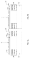
- Fig. 4A is a diagram showing propagation of light out of assembly 100 in a transmission mode
- Fig. 4B is a diagram showing propagation of light into assembly 100 in a reception mode.
- the transmission mode light propagates along waveguide 112 in a surface propagating mode and is emitted from grating out-coupler 102 in a direction dependent on a tilt angle of grating out-coupler 102 and substantially perpendicular to the direction of transmission through waveguide 112.
- the reception mode light is received at grating out-coupler 102, and transmitted along waveguide 112 in a surface-propagating mode in a direction substantially perpendicular to the direction of the light being received at grating out-coupler 102.
- grating out-coupler 102 may be used in optical communication applications to couple light into and/or out of waveguide 112 for transmission to and/or transmission from transmitter/receiver 113 (shown in Fig. 1 ).
- assembly 100 includes a single grating out-coupler 102 that optically couples light to/from transmitter/receiver 113.
- assemblies in other implementations may include multiple grating out-couplers.
- Fig. 5 is a plan view of an alternative grating out-coupler assembly 500.
- Assembly 500 includes a first grating out-coupler 502 on a first tiltable surface 504 (such as grating out coupler 102 and tiltable surface 104), and a second grating out-coupler 506 on a second tiltable surface 508. Similar to assembly 100, first tiltable surface 504 is tiltable using a first actuator 510, and second tiltable surface 508 is tiltable using a second actuator 512.
- first grating out-coupler 502 functions as a transmission element to couple light out of a transmitter 520
- second grating out-coupler 506 functions as a reception element to couple light into a receiver 522.
- first grating out-coupler 502 and second grating out-coupler 506 may be tilted at the same or different orientations. This allows assembly 500 to isolate a return signal from a specific direction (e.g., the same direction in which a signal is transmitted from assembly 500), which facilitates preventing interference from other units.
- Fig. 6 is a plan view of another alternative grating out-coupler assembly 600.
- Assembly 600 includes a first grating out-coupler 602 and second grating out-coupler 604 that are both on a tiltable surface 606.
- Tiltable surface 606 is tilted using an actuator 610, similar to actuator 106 (shown in Fig. 1 ).
- first grating out-coupler 602 functions as a transmission element
- second grating out-coupler 604 functions as a reception element.
- Including both transmission and reception elements in the same assembly permits assembly 600 to be used in a system-on-a-chip application, such as in a FMCW LIDAR system.
- first grating out-coupler 602 and second grating out-coupler 604 are on the same tiltable surface 606, first grating out-coupler 602 and second grating out-coupler 604 are tilted at the same orientation, using the same actuator 610, substantially eliminating any errors in synching the orientation of first grating out-coupler 602 and second grating out-coupler 604.
- Fig. 7 is a block diagram of an exemplary LIDAR system 700 that includes a tiltable grating out-coupler assembly 702, such as assembly 100 (shown in Fig. 1 ), assembly 500 (shown in Fig. 5 ), or assembly 600 (shown in Fig. 6 ).
- Assembly 702 is coupled to a photonic circuit 704 for transmitting signals from and/or receiving signals at photonic circuit 704.
- Photonic circuit 704 may include, for example, transmitter/receiver 113 (shown in Fig. 1 ).
- LIDAR system 700 may be, for example, a chip-scale frequency modulated continues wavelength (FMCW) LIDAR.
- LIDAR system 700 may be used, for example, for range-finding applications (e.g., used by autonomous vehicles), biological applications, directed energy applications, and/or communications applications.
- range-finding applications e.g., used by autonomous vehicles
- biological applications e.g., directed energy applications, and/or communications applications.
- Fig. 8 is a flowchart of an exemplary method 800 for assembling a LIDAR system, such as LIDAR system 700.
- Method 800 includes suspending 802 a tiltable surface above a cavity formed in a substrate, the tiltable surface suspended using an actuator configured to selectively control a pitch of the tiltable surface.
- the substrate may be formed using a chemical vapor deposition process.
- Method 800 further includes positioning 804 a grating out-coupler on the tiltable surface.
- Method 800 further includes optically coupling 806 the grating out-coupler to a photonic circuit.
- Fig. 9 is a perspective view of an alternative grating out-coupler assembly 900.
- assembly 900 does not include a cavity. Instead, a grating out-coupler 902 rests on a tiltable surface 904 that is elevated and suspended above a substrate 910 by a plurality of actuators 906.
- tiltable surface 904 is suspended by four actuators 906 that may be selectively manipulated to orient tiltable surface 904 at a plurality of different orientations.
- assembly 900 may include any suitable number and type of actuators 906.
- grating out-coupler 902 is optically coupled to a waveguide 912 via an optical taper 914.
- waveguide 912 passes through tiltable surface 904 and runs along one actuator 906.
- the grating out-coupler assemblies described herein may be fabricated monolithically with the remainder of a photonic circuit. This facilitates avoiding costly and error-prone steps generally required to integrate optical elements needed to steer a beam of light, such as bonding of additional reflectors (which requires very accurate alignment to function properly).
- Known structures also introduce optical losses at each interface. These losses are avoided using the systems and methods described herein due to the integrated nature of the assembly. Losses reduced by the systems and methods described herein include imperfect reflectivity at mirror surfaces, absorption in bonding media, and wavefront distortion due to mirror imperfections. In particular, eliminating wavefront distortion enables achieving higher signal-to-noise ratios and resolution in coherent detection application, because a phase relationship is substantially maintained across the entire signal.
Landscapes
- Physics & Mathematics (AREA)
- General Physics & Mathematics (AREA)
- Engineering & Computer Science (AREA)
- Optics & Photonics (AREA)
- Computer Networks & Wireless Communication (AREA)
- Radar, Positioning & Navigation (AREA)
- Remote Sensing (AREA)
- Microelectronics & Electronic Packaging (AREA)
- Optical Integrated Circuits (AREA)
- Mechanical Light Control Or Optical Switches (AREA)
- Optical Couplings Of Light Guides (AREA)
- Optical Radar Systems And Details Thereof (AREA)
Abstract
Description
- The field of the disclosure relates generally to optical communications, and, more particularly, to assemblies that facilitate selectively tilting a grating out-coupler.
- At least some known LIDAR systems include a microelectromechanical system (MEMS) mirror. The MEMS mirror may be actuatable using an applied voltage. This actuated MEMS mirror may be used to steer a laser beam for measuring the range of objects within a field of view. However, properly aligning the MEMS mirror may be relatively difficult, resulting in relatively high interference and a poor signal-to-noise ratio.
- In one aspect, a grating out-coupler assembly is provided. The grating out-coupler assembly includes a substrate, a tiltable surface suspended above the substrate, an actuator configured to selectively control a pitch of the tiltable surface, and a grating out-coupler supported by the tiltable surface.
- In another aspect, a LIDAR system is provided. The LIDAR system includes a photonic circuit, and a grating out-coupler assembly coupled to the photonic circuit, the grating out-coupler assembling including a substrate, a tiltable surface suspended above the substrate, an actuator configured to selectively control a pitch of the tiltable surface; and a grating out-coupler supported by the tiltable surface.
- In yet another aspect, a method of assembling a LIDAR system is provided. The method includes suspending a tiltable surface above a substrate, the tiltable surface suspended using an actuator configured to selectively control a pitch of the tiltable surface, positioning a grating out-coupler on the tiltable surface, and optically coupling the grating out-coupler to a photonic circuit.
-
-
Fig. 1 is a plan view of an exemplary tiltable grating out-coupler assembly. -
Fig. 2 is a perspective view of the assembly shown inFig. 1 . -
Fig. 3 is a perspective view of the assembly shown inFig. 2 showing a cross-section of the assembly. -
Fig. 4A is a diagram showing propagation of light through the assembly shown inFig. 1 in a transmission mode. -
Fig. 4B is a diagram showing propagation of light through the assembly shown inFig. 1 in a reception mode. -
Fig. 5 is a plan view of an alternative tiltable grating out-coupler assembly. -
Fig. 6 is a plan view of an alternative tiltable grating out-coupler assembly. -
Fig. 7 is a block diagram of an exemplary LIDAR system that includes a tiltable grating out-coupler assembly. -
Fig. 8 is a flowchart of an exemplary method for assembling a LIDAR system. -
Fig. 9 is a perspective view of an alternative tiltable grating out-coupler assembly. - The systems and methods described herein provide a grating out-coupler assembly. The assembly includes a tiltable surface suspended above a cavity formed in a substrate. A grating out-coupler is formed on the tiltable surface. Using one or more actuators (e.g., torsion bars), the tiltable surface can be rotated such that an orientation of the grating out-coupler is adjusted. The grating out-coupler may be coupled to a photonic circuit for use as a transmission element or a reception element. As used herein, a grating out-coupler refers to a microelectromechanical system (MEMS) device that is configured to couple light into and/or out of a waveguide.
-
Fig. 1 is a plan view of an exemplary tiltable grating out-coupler assembly 100.Fig. 2 is a perspective view ofassembly 100. As shown inFigs. 1 and2 ,assembly 100 includes a grating out-coupler 102 that rests on atiltable surface 104. Anactuator 106 coupled totiltable surface 104 facilitates controlling a pitch oftiltable surface 104.Tiltable surface 104 may rest atopactuator 106, or alternatively,actuator 106 may extend throughtiltable surface 104. In the exemplary implementation,actuator 106 is a torsion bar. Specifically, rotatingactuator 106 along alongitudinal axis 107 ofactuator 106 causes the pitch oftiltable surface 104 to change. That is,actuator 106 is made from a relatively flexible material that allowsactuator 106 to twist and rotate aboutlongitudinal axis 107. In the exemplary implementation, tiltable surface 104 (and by extension grating out-coupler 102) is capable of one-dimensional tilt (i.e., aboutlongitudinal axis 107 of actuator 106). Alternatively, in other implementations,assembly 100 may include external gimbals or other actuators that enable two-dimensional tilt. - As shown in
Fig. 2 , inassembly 100,tiltable surface 104 is suspended byactuator 106 above asubstrate 110, and in particular, above acavity 108 formed insubstrate 110.Cavity 108 allowstiltable surface 104 to be tilted without contactingsubstrate 110.Cavity 108 may have a depth of approximately 15 microns (µm) and length and width dimensions (i.e., in directions parallel to a plane formed by tiltable surface 104) of approximately 2 millimeters (mm) by 2 mm. Alternatively,cavity 108 may have any suitable dimensions. In some embodiments, the depth ofcavity 108 extends through theentire substrate 110. Alternatively, the depth ofcavity 108 may only extend through a portion ofsubstrate 110, as seen best inFig. 3 . Further, in some embodiments,assembly 100 may not includecavity 108. Instead,tiltable surface 104 may be suspended abovesubstrate 110 using sacrificial layers (e.g., for a silicon substrate, a silicon oxide layer and a silicon layer) that are grown and then etched away selectively to formtiltable surface 104. - To facilitate transmitting and receiving optical signals, in the exemplary implementation, grating out-
coupler 102 is coupled to awaveguide 112 via anoptical taper 114.Optical taper 114 is a device configured to expand a width of the optical mode fromwaveguide 112 to grating out-coupler 102 when transmitting light fromassembly 100, and is configured to compress the width of the optical mode from grating out-coupler to waveguide 112 when receiving light atassembly 100. For example, assumewaveguide 112 has a first width, w1. Accordingly, the mode of the light withinwaveguide 112 is confined within a cross-section of w1*z (where z is a depth dimension). The light entersoptical taper 114, which adiabatically expands the width of the optical mode until it reaches a second width, w2. Now the light is confined within a cross-section of w2*z. The second width w2 is matched to the width of grating out-coupler 102. For light received asassembly 100,optical taper 114 adiabatically compresses a width of the optical mode from w2 to w1. Accordingly,optical taper 114 bridges the differing widths betweenwaveguide 112 and grating out-coupler 102 with minimum loss. - In the exemplary implementation,
waveguide 112 extends across a portion ofactuator 106. Specifically,waveguide 112 is positioned atopactuator 106, and is also made of a flexible material, such that whenactuator 106 is twisted aboutlongitudinal axis 107, a portion ofwaveguide 112 also twists. Notably, the twisting ofwaveguide 112 does not significantly affect the light propagating abilities ofwaveguide 112. Waveguide 112 couples grating out-coupler 102 to an optical transmitter and/orreceiver 113. Although transmitter/receiver 113 is shown schematically onsubstrate 110, those of skill will appreciate that transmitter/receiver 113 may be separate fromassembly 100. Light propagates into and out of grating out-coupler 102 along afirst direction 116, and propagates withinwaveguide 112 along asecond direction 118 that is substantially orthogonal tofirst direction 116. That is, grating out-coupler 102 absorbs/emits light in a direction normal to a plane formed by grating out-coupler 102. -
Fig. 3 is a perspective view ofassembly 100 showing a cross-section ofassembly 100. As shown inFig. 2 , a plurality ofparallel grooves 302 are formed in grating out-coupler 102 to form agrating structure 304. In the exemplary implementation, to facilitate optical coupling, grating out-coupler 102,optical taper 114, andwaveguide 112 are formed from afirst material 310 having a relatively high refractive index (e.g., silicon, poly-silicon, gallium arsenide, etc.) on top of a second, lower index material 312 (e.g., aluminum oxide, silicon oxide, etc.). For example, gratingstructure 304 may be formed by forminggrooves 302 infirst material 310, but not insecond material 312. In one example,first material 310 has a refractive index greater than 2.5 andsecond material 312 has a refractive index in a range from approximately 1.5 to 2.5. Alternatively, first andsecond materials actuator 106,tiltable surface 104, andsubstrate 110 are be formed using an alternating structure of polysilicon and silicon oxide layers. - As shown in
Fig. 3 ,substrate 110 includes a plurality of MEMS layers 320 formed on top of abase 322. In the exemplary implementation, MEMS layers 320 include alternating layers of silicon and silicon oxide, andbase 322 is silicon. Alternatively, MEMS layers 320 andbase 322 may be formed of any suitable material. -
Substrate 110 may be formed, for example, using a chemical vapor deposition process, in which base 322 andMEMS layers 320 are formed by depositing lattices of silicon and silicon oxide. The deposition process will form a cuboid structure, andcavity 108 may be formed by removing material from the cuboid structure. The dimensions ofcavity 108,base 322, andMEMS layers 320 will vary based on the wavelength of light being coupled using grating out-coupler 102. -
Fig. 4A is a diagram showing propagation of light out ofassembly 100 in a transmission mode, andFig. 4B is a diagram showing propagation of light intoassembly 100 in a reception mode. In the transmission mode, light propagates alongwaveguide 112 in a surface propagating mode and is emitted from grating out-coupler 102 in a direction dependent on a tilt angle of grating out-coupler 102 and substantially perpendicular to the direction of transmission throughwaveguide 112. In the reception mode, light is received at grating out-coupler 102, and transmitted alongwaveguide 112 in a surface-propagating mode in a direction substantially perpendicular to the direction of the light being received at grating out-coupler 102. As described above, grating out-coupler 102 may be used in optical communication applications to couple light into and/or out ofwaveguide 112 for transmission to and/or transmission from transmitter/receiver 113 (shown inFig. 1 ). - In the implementation shown in
Figs. 1-4B ,assembly 100 includes a single grating out-coupler 102 that optically couples light to/from transmitter/receiver 113. Alternatively, assemblies in other implementations may include multiple grating out-couplers. For example,Fig. 5 is a plan view of an alternative grating out-coupler assembly 500.Assembly 500 includes a first grating out-coupler 502 on a first tiltable surface 504 (such as grating outcoupler 102 and tiltable surface 104), and a second grating out-coupler 506 on a secondtiltable surface 508. Similar toassembly 100, firsttiltable surface 504 is tiltable using afirst actuator 510, and secondtiltable surface 508 is tiltable using asecond actuator 512. - In the exemplary implementation, first grating out-
coupler 502 functions as a transmission element to couple light out of atransmitter 520, and second grating out-coupler 506 functions as a reception element to couple light into areceiver 522. Including both transmission and reception elements in the same assembly permitsassembly 500 to be used in a system-on-a-chip application, such as in a frequency-modulated continuous-wave (FMCW) LIDAR system. Further, first grating out-coupler 502 and second grating out-coupler 506 may be tilted at the same or different orientations. This allows assembly 500 to isolate a return signal from a specific direction (e.g., the same direction in which a signal is transmitted from assembly 500), which facilitates preventing interference from other units. -
Fig. 6 is a plan view of another alternative grating out-coupler assembly 600.Assembly 600 includes a first grating out-coupler 602 and second grating out-coupler 604 that are both on atiltable surface 606.Tiltable surface 606 is tilted using anactuator 610, similar to actuator 106 (shown inFig. 1 ). In the exemplary implementation, first grating out-coupler 602 functions as a transmission element, and second grating out-coupler 604 functions as a reception element. Including both transmission and reception elements in the same assembly permitsassembly 600 to be used in a system-on-a-chip application, such as in a FMCW LIDAR system. Notably, because first grating out-coupler 602 and second grating out-coupler 604 are on the sametiltable surface 606, first grating out-coupler 602 and second grating out-coupler 604 are tilted at the same orientation, using thesame actuator 610, substantially eliminating any errors in synching the orientation of first grating out-coupler 602 and second grating out-coupler 604. -
Fig. 7 is a block diagram of anexemplary LIDAR system 700 that includes a tiltable grating out-coupler assembly 702, such as assembly 100 (shown inFig. 1 ), assembly 500 (shown inFig. 5 ), or assembly 600 (shown inFig. 6 ).Assembly 702 is coupled to aphotonic circuit 704 for transmitting signals from and/or receiving signals atphotonic circuit 704.Photonic circuit 704 may include, for example, transmitter/receiver 113 (shown inFig. 1 ).LIDAR system 700 may be, for example, a chip-scale frequency modulated continues wavelength (FMCW) LIDAR.LIDAR system 700 may be used, for example, for range-finding applications (e.g., used by autonomous vehicles), biological applications, directed energy applications, and/or communications applications. -
Fig. 8 is a flowchart of anexemplary method 800 for assembling a LIDAR system, such asLIDAR system 700.Method 800 includes suspending 802 a tiltable surface above a cavity formed in a substrate, the tiltable surface suspended using an actuator configured to selectively control a pitch of the tiltable surface. As described above, the substrate may be formed using a chemical vapor deposition process.Method 800 further includes positioning 804 a grating out-coupler on the tiltable surface.Method 800 further includes optically coupling 806 the grating out-coupler to a photonic circuit. -
Fig. 9 is a perspective view of an alternative grating out-coupler assembly 900. As compared toassembly 100,assembly 900 does not include a cavity. Instead, a grating out-coupler 902 rests on atiltable surface 904 that is elevated and suspended above asubstrate 910 by a plurality ofactuators 906. In the exemplary implementation,tiltable surface 904 is suspended by fouractuators 906 that may be selectively manipulated to orienttiltable surface 904 at a plurality of different orientations. Alternatively,assembly 900 may include any suitable number and type ofactuators 906. Similar to grating out-coupler 102, grating out-coupler 902 is optically coupled to awaveguide 912 via anoptical taper 914. In this implementation,waveguide 912 passes throughtiltable surface 904 and runs along oneactuator 906. - Notably, the grating out-coupler assemblies described herein may be fabricated monolithically with the remainder of a photonic circuit. This facilitates avoiding costly and error-prone steps generally required to integrate optical elements needed to steer a beam of light, such as bonding of additional reflectors (which requires very accurate alignment to function properly). Known structures also introduce optical losses at each interface. These losses are avoided using the systems and methods described herein due to the integrated nature of the assembly. Losses reduced by the systems and methods described herein include imperfect reflectivity at mirror surfaces, absorption in bonding media, and wavefront distortion due to mirror imperfections. In particular, eliminating wavefront distortion enables achieving higher signal-to-noise ratios and resolution in coherent detection application, because a phase relationship is substantially maintained across the entire signal.
- Further, the disclosure comprises embodiments according to the following clauses:
- Clause 1. A grating out-coupler assembly comprising:
- a substrate;
- a tiltable surface suspended above said substrate;
- an actuator configured to selectively control a pitch of said tiltable surface; and
- a grating out-coupler supported by said tiltable surface.
- Clause 2. A grating out-coupler assembly in accordance with Clause 1, further comprising a waveguide coupling said grating out-coupler to one of a transmitter and a receiver of a photonic circuit.
- Clause 3. A grating out-coupler assembly in accordance with any preceding Clause, in particular Clause 1, further comprising a second grating out-coupler.
- Clause 4. A grating out-coupler assembly in accordance with Clause 3, wherein said grating out-coupler is configured to function as a transmission element, and wherein said second grating out-coupler is configured to function as a reception element.
-
Clause 5. A grating out-coupler assembly in accordance with Clause 3 or 4, wherein said tiltable surface supports both said grating out-coupler and said second grating out-coupler. - Clause 6. A grating out-coupler assembly in accordance with
Clause 3, 4 or 5, further comprising:- a second tiltable surface supporting said second grating out-coupler; and
- a second actuator configured to selectively control a pitch of said second tiltable surface.
- Clause 7. A grating out-coupler assembly in accordance with any preceding Clause, in particular Clause 1, wherein a pitch of said tiltable surface is adjustable independent of a pitch of said second tiltable surface.
- Clause 8. A grating out-coupler assembly in accordance with any preceding Clause, in particular Clause 1, wherein said actuator comprises a torsion bar that suspends said tiltable surface above a cavity formed in said substrate.
- Clause 9. A LIDAR system comprising:
- a photonic circuit; and
- a grating out-coupler assembly coupled to said photonic circuit, said grating out-coupler assembling comprising:
- a substrate;
- a tiltable surface suspended above said substrate;
- an actuator configured to selectively control a pitch of said tiltable surface; and
- a grating out-coupler supported by said tiltable surface.
- Clause 10. A LIDAR system in accordance with Clause 9, wherein said grating out-coupler further comprises a waveguide coupling said grating out-coupler to one of a transmitter and a receiver of said photonic circuit.
- Clause 11. A LIDAR system in accordance with Clause 9 or 10, wherein said grating out-coupler assembly comprises a second grating out-coupler.
- Clause 12. A LIDAR system in accordance with Clause 11, wherein said grating out-coupler is configured to function as a transmission element, and wherein said second grating out-coupler is configured to function as a reception element.
- Clause 13. A LIDAR system in accordance with Clause 11 or 12, wherein said tiltable surface supports both said grating out-coupler and said second grating out-coupler.
- Clause 14. A LIDAR system in accordance with Clause 11, 12 or 13, wherein said grating out-coupler assembly comprises:
- a second tiltable surface supporting said second grating out-coupler; and
- a second actuator configured to selectively control a pitch of said second tiltable surface.
- Clause 15. A LIDAR system in accordance with Clause 14, wherein a pitch of said tiltable surface is adjustable independent of a pitch of said second tiltable surface.
- Clause 16. A LIDAR system in accordance with any preceding Clause, in particular Clause 9, wherein said actuator comprises a torsion bar that suspends said tiltable surface above a cavity formed in said substrate.
- Clause 17. A method of assembling a LIDAR system, said method comprising:
- suspending a tiltable surface above a substrate, the tiltable surface suspended using an actuator configured to selectively control a pitch of the tiltable surface;
- positioning a grating out-coupler on the tiltable surface; and
- optically coupling the grating out-coupler to a photonic circuit.
- Clause 18. A method in accordance with Clause 17, further comprising positioning a second grating out-coupler on a second tiltable surface.
- Clause 19. A method in accordance with Clause 18, further comprising adjusting pitches of the tiltable surface and the second tiltable surface independent of one another.
- Clause 20. A method in accordance with Clause 17, 18 or 19, further comprising positioning a second grating out-coupler on the tiltable surface.
- This written description uses examples to disclose various implementations, which include the best mode, to enable any person skilled in the art to practice those implementations, including making and using any devices or systems and performing any incorporated methods. The patentable scope is defined by the claims, and may include other examples that occur to those skilled in the art. Such other examples are intended to be within the scope of the claims if they have structural elements that do not differ from the literal language of the claims, or if they include equivalent structural elements with insubstantial differences from the literal language of the claims.
Claims (13)
- A grating out-coupler assembly (100,500) comprising:a substrate (110);a tiltable surface (104,504) suspended above said substrate (110);an actuator (106/510) configured to selectively control a pitch of said tiltable surface (104/504); anda grating out-coupler (102,502) supported by said tiltable surface (104/504).
- A grating out-coupler assembly (100,500) in accordance with Claim 1, further comprising a waveguide (112) coupling said grating out-coupler (102) to one of a transmitter (113) and a receiver (113) of a photonic circuit (704).
- A grating out-coupler assembly (500) in accordance with any of Claims 1 to 2, further comprising a second grating out-coupler (506).
- A grating out-coupler assembly (500) in accordance with any of Claims 1 to 3, wherein said grating out-coupler (502) is configured to function as a transmission element (520), and wherein said second grating out-coupler 506 is configured to function as a reception element (522).
- A grating out-coupler assembly (500) in accordance with any of Claims 1 to 4, wherein said tiltable surface (504) supports both said grating out-coupler (502) and said second grating out-coupler (506).
- A grating out-coupler assembly (500) in accordance with any of Claims 1 to 5, further comprising:a second tiltable surface (508) supporting said second grating out-coupler (506); anda second actuator (512) configured to selectively control a pitch of said second tiltable surface (508).
- A grating out-coupler assembly (500) in accordance with any of Claims 1 to 6, wherein a pitch of said tiltable surface (504) is adjustable independent of a pitch of said second tiltable surface (508).
- A grating out-coupler assembly (100,500) in accordance with any of Claims 1 to 7, wherein said actuator (106) comprises a torsion bar that suspends said tiltable surface (104) above a cavity (108) formed in said substrate (110).
- A LIDAR system (700) comprising a photonic circuit (704); and
the grating out-coupler assembly (100,500,600) of Claims 1 to 8 coupled to said photonic circuit (704). - A method of assembling a LIDAR system (700), said method comprising:suspending a tiltable surface (104,504) above a substrate (110), the tiltable surface (104,504,606) suspended using an actuator (105,510) configured to selectively control a pitch of the tiltable surface (104,606);positioning a grating out-coupler (102,502) on the tiltable surface (104,504); andoptically coupling the grating out-coupler (102,502) to a photonic circuit (704).
- A method in accordance with Claim 10, further comprising positioning a second grating out-coupler 506 on a second tiltable surface (508).
- A method in accordance with any of Claims 10 to 11, further comprising adjusting pitches of the tiltable surface (504) and the second tiltable surface (508) independent of one another.
- A method in accordance with any of Claims 10 to 12, further comprising positioning a second grating out-coupler (604) on the tiltable surface (606).
Applications Claiming Priority (1)
| Application Number | Priority Date | Filing Date | Title |
|---|---|---|---|
| US14/944,621 US9746611B2 (en) | 2015-11-18 | 2015-11-18 | Systems and methods for tiltable grating out-couplers |
Publications (2)
| Publication Number | Publication Date |
|---|---|
| EP3171198A1 true EP3171198A1 (en) | 2017-05-24 |
| EP3171198B1 EP3171198B1 (en) | 2020-06-10 |
Family
ID=57046942
Family Applications (1)
| Application Number | Title | Priority Date | Filing Date |
|---|---|---|---|
| EP16181404.1A Active EP3171198B1 (en) | 2015-11-18 | 2016-07-27 | Systems and methods for tiltable grating out-couplers |
Country Status (4)
| Country | Link |
|---|---|
| US (1) | US9746611B2 (en) |
| EP (1) | EP3171198B1 (en) |
| JP (1) | JP6924014B2 (en) |
| IL (1) | IL247061B (en) |
Families Citing this family (15)
| Publication number | Priority date | Publication date | Assignee | Title |
|---|---|---|---|---|
| US10788582B2 (en) * | 2018-05-11 | 2020-09-29 | Silc Technologies, Inc. | Optical sensor chip |
| US11536805B2 (en) | 2018-06-25 | 2022-12-27 | Silc Technologies, Inc. | Optical switching for tuning direction of LIDAR output signals |
| US12535586B2 (en) | 2018-08-31 | 2026-01-27 | SiLC Technology, Inc. | Reduction of ADC sampling rates in LIDAR systems |
| US12429569B2 (en) | 2019-05-17 | 2025-09-30 | Silc Technologies, Inc. | Identification of materials illuminated by LIDAR systems |
| US11650317B2 (en) | 2019-06-28 | 2023-05-16 | Silc Technologies, Inc. | Use of frequency offsets in generation of LIDAR data |
| EP4155760B1 (en) * | 2020-06-26 | 2025-04-02 | Mitsubishi Electric Corporation | Optical scanning device and ranging apparatus |
| DE102021201373A1 (en) | 2021-02-12 | 2022-08-18 | Fraunhofer-Gesellschaft zur Förderung der angewandten Forschung eingetragener Verein | MEMS-actuated light-emitting device and method for changing the position of a light-emitting device |
| JP2022144256A (en) * | 2021-03-18 | 2022-10-03 | 株式会社リコー | Optical scanner, object detection device and moving body |
| US12541009B2 (en) | 2021-06-17 | 2026-02-03 | Silc Technologies, Inc. | Scanning multiple LIDAR system output signals |
| US12411213B2 (en) | 2021-10-11 | 2025-09-09 | Silc Technologies, Inc. | Separation of light signals in a LIDAR system |
| US12553995B2 (en) | 2022-02-14 | 2026-02-17 | Silc Technologies, Inc. | Data refinement in optical systems |
| US12578443B2 (en) | 2022-04-23 | 2026-03-17 | Silc Technologies, Inc. | Data refinement in optical imaging systems |
| US12422618B2 (en) | 2022-10-13 | 2025-09-23 | Silc Technologies, Inc. | Buried taper with reflecting surface |
| US12578439B2 (en) | 2023-04-11 | 2026-03-17 | Silc Technologies, Inc. | Increasing resolution in imaging systems |
| US20260063844A1 (en) * | 2024-09-05 | 2026-03-05 | Globalfoundries U.S. Inc. | Photodetectors with an integrated grating coupler |
Citations (3)
| Publication number | Priority date | Publication date | Assignee | Title |
|---|---|---|---|---|
| US5003550A (en) * | 1990-03-09 | 1991-03-26 | Spectra Diode Laboratories, Inc. | Integrated laser-amplifier with steerable beam |
| JPH05232519A (en) * | 1991-02-14 | 1993-09-10 | Ibiden Co Ltd | Optical deflecting element |
| JPH10111524A (en) * | 1996-10-04 | 1998-04-28 | Minolta Co Ltd | Optical deflector and scanning optical device using the optical deflector |
Family Cites Families (10)
| Publication number | Priority date | Publication date | Assignee | Title |
|---|---|---|---|---|
| JP2509245B2 (en) * | 1987-09-16 | 1996-06-19 | 株式会社トプコン | Lightwave rangefinder |
| JPH02191916A (en) * | 1988-09-19 | 1990-07-27 | Hitachi Ltd | Optical head and optical information processing device |
| US5684631A (en) * | 1996-05-13 | 1997-11-04 | Lucent Technologies Inc. | Optical modulator/switch including reflective zone plate and related method of use |
| US9086229B1 (en) | 2006-10-13 | 2015-07-21 | Hrl Laboratories, Llc | Optical components from micro-architected trusses |
| US7382959B1 (en) | 2006-10-13 | 2008-06-03 | Hrl Laboratories, Llc | Optically oriented three-dimensional polymer microstructures |
| US9606273B2 (en) * | 2012-01-11 | 2017-03-28 | Lumentum Operations Llc | Diffractive MEMS device |
| JP5697699B2 (en) * | 2013-03-08 | 2015-04-08 | キヤノン株式会社 | Raman scattering measuring apparatus and Raman scattering measuring method |
| US10150665B2 (en) * | 2013-03-15 | 2018-12-11 | The Board Of Trustees Of The Leland Stanford Junior University | In-plane-strain-actuated out-of-plane actuator |
| JP5907146B2 (en) * | 2013-11-22 | 2016-04-20 | 株式会社豊田中央研究所 | Optical device |
| US9404860B2 (en) * | 2014-05-09 | 2016-08-02 | Apple Inc. | Micro-electro-mechanical system optical sensor with tilt plates |
-
2015
- 2015-11-18 US US14/944,621 patent/US9746611B2/en active Active
-
2016
- 2016-07-27 EP EP16181404.1A patent/EP3171198B1/en active Active
- 2016-08-02 IL IL247061A patent/IL247061B/en active IP Right Grant
- 2016-11-08 JP JP2016217772A patent/JP6924014B2/en active Active
Patent Citations (3)
| Publication number | Priority date | Publication date | Assignee | Title |
|---|---|---|---|---|
| US5003550A (en) * | 1990-03-09 | 1991-03-26 | Spectra Diode Laboratories, Inc. | Integrated laser-amplifier with steerable beam |
| JPH05232519A (en) * | 1991-02-14 | 1993-09-10 | Ibiden Co Ltd | Optical deflecting element |
| JPH10111524A (en) * | 1996-10-04 | 1998-04-28 | Minolta Co Ltd | Optical deflector and scanning optical device using the optical deflector |
Non-Patent Citations (3)
| Title |
|---|
| MENG-HSIUNG KIANG ET AL: "Surface-micromachined diffraction gratings for scanning spectroscopic applications", INTERNATIONAL CONFERENCE ON SOLID-STATE SENSORS AND ACTUATORS; [INTERNATIONAL CONFERENCE ON SOLID-STATE SENSORS AND ACTUATORS. DIGEST OF TECHNICAL PAPERS], NEW YORK, NY : IEEE; US, vol. 1, 16 June 1997 (1997-06-16), pages 343 - 345, XP010240480, ISBN: 978-0-7803-3829-6, DOI: 10.1109/SENSOR.1997.613654 * |
| TAO J F ET AL: "Ultra-high coupling efficiency of MEMS tunable laser via 3-dimensional micro-optical coupling system", IEEE 24TH INTERNATIONAL CONFERENCE ON MICRO ELECTRO MECHANICAL SYSTEMS (MEMS 2011), IEEE, US, 23 January 2011 (2011-01-23), pages 13 - 16, XP031982338, ISBN: 978-1-4244-9632-7, DOI: 10.1109/MEMSYS.2011.5734350 * |
| YU DU ET AL: "A 21.5kHz high optical resolution electrostatic double-layered vibratory grating laser scanner", SENSORS AND ACTUATORS A: PHYSICAL, ELSEVIER BV, NL, vol. 168, no. 2, 2 April 2011 (2011-04-02), pages 253 - 261, XP028386469, ISSN: 0924-4247, [retrieved on 20110408], DOI: 10.1016/J.SNA.2011.04.007 * |
Also Published As
| Publication number | Publication date |
|---|---|
| EP3171198B1 (en) | 2020-06-10 |
| IL247061A0 (en) | 2016-12-29 |
| IL247061B (en) | 2021-05-31 |
| JP6924014B2 (en) | 2021-08-25 |
| US20170139141A1 (en) | 2017-05-18 |
| US9746611B2 (en) | 2017-08-29 |
| JP2017097340A (en) | 2017-06-01 |
Similar Documents
| Publication | Publication Date | Title |
|---|---|---|
| EP3171198B1 (en) | Systems and methods for tiltable grating out-couplers | |
| KR100908623B1 (en) | Optical bonding apparatus and method using transversal transmission of light output | |
| EP3171207B1 (en) | Photonic chip grating couplers | |
| CN107003513B (en) | Light beam scanner | |
| US7250317B2 (en) | Method of fabricating optical waveguide reflectors | |
| EP3296783B1 (en) | Integrated photonics waveguide grating coupler | |
| US20180120422A1 (en) | Low cost and compact optical phased array with electro-optic beam steering | |
| JP2015118372A (en) | Radiation coupler | |
| US9348092B1 (en) | Mode size converters for reducing a modal profile of incoming light | |
| US8452141B2 (en) | Optical waveguide coupling device and associated methods | |
| WO2016172970A1 (en) | Polarization rotator and optical signal processing method | |
| WO2013122945A1 (en) | Coupling between optical devices | |
| US12092880B2 (en) | Beam steering structure with integrated polarization splitter | |
| JP5590794B2 (en) | System and method for fiber-based resonator coupling | |
| US20220021473A1 (en) | System and method for terahertz polarization-division multiplexing | |
| US12019274B2 (en) | Polarization rotator | |
| US7289702B2 (en) | Optical waveguide apparatus | |
| US6944368B2 (en) | Waveguide-to-semiconductor device coupler | |
| JPH1068916A (en) | Optical waveguide device and method of manufacturing the same | |
| US20040247245A1 (en) | Bidirectional optical communication module with a reflector | |
| US20150323819A1 (en) | Electro-optic modulators | |
| TW200409982A (en) | Variable optical attenuator in micro-electro-mechanical systems and method of making the same | |
| US20220350084A1 (en) | Optical Connecting Structure | |
| HK40090808A (en) | Optical beam scanner |
Legal Events
| Date | Code | Title | Description |
|---|---|---|---|
| PUAI | Public reference made under article 153(3) epc to a published international application that has entered the european phase |
Free format text: ORIGINAL CODE: 0009012 |
|
| STAA | Information on the status of an ep patent application or granted ep patent |
Free format text: STATUS: REQUEST FOR EXAMINATION WAS MADE |
|
| 17P | Request for examination filed |
Effective date: 20160727 |
|
| AK | Designated contracting states |
Kind code of ref document: A1 Designated state(s): AL AT BE BG CH CY CZ DE DK EE ES FI FR GB GR HR HU IE IS IT LI LT LU LV MC MK MT NL NO PL PT RO RS SE SI SK SM TR |
|
| AX | Request for extension of the european patent |
Extension state: BA ME |
|
| RBV | Designated contracting states (corrected) |
Designated state(s): AL AT BE BG CH CY CZ DE DK EE ES FI FR GB GR HR HU IE IS IT LI LT LU LV MC MK MT NL NO PL PT RO RS SE SI SK SM TR |
|
| GRAP | Despatch of communication of intention to grant a patent |
Free format text: ORIGINAL CODE: EPIDOSNIGR1 |
|
| STAA | Information on the status of an ep patent application or granted ep patent |
Free format text: STATUS: GRANT OF PATENT IS INTENDED |
|
| RIC1 | Information provided on ipc code assigned before grant |
Ipc: G02B 6/124 20060101ALI20191205BHEP Ipc: G02B 26/08 20060101ALI20191205BHEP Ipc: G02B 6/30 20060101ALI20191205BHEP Ipc: G01S 7/481 20060101AFI20191205BHEP |
|
| INTG | Intention to grant announced |
Effective date: 20200108 |
|
| GRAS | Grant fee paid |
Free format text: ORIGINAL CODE: EPIDOSNIGR3 |
|
| GRAA | (expected) grant |
Free format text: ORIGINAL CODE: 0009210 |
|
| STAA | Information on the status of an ep patent application or granted ep patent |
Free format text: STATUS: THE PATENT HAS BEEN GRANTED |
|
| AK | Designated contracting states |
Kind code of ref document: B1 Designated state(s): AL AT BE BG CH CY CZ DE DK EE ES FI FR GB GR HR HU IE IS IT LI LT LU LV MC MK MT NL NO PL PT RO RS SE SI SK SM TR |
|
| REG | Reference to a national code |
Ref country code: GB Ref legal event code: FG4D |
|
| REG | Reference to a national code |
Ref country code: CH Ref legal event code: EP Ref country code: AT Ref legal event code: REF Ref document number: 1279617 Country of ref document: AT Kind code of ref document: T Effective date: 20200615 |
|
| REG | Reference to a national code |
Ref country code: DE Ref legal event code: R096 Ref document number: 602016037800 Country of ref document: DE |
|
| REG | Reference to a national code |
Ref country code: IE Ref legal event code: FG4D |
|
| REG | Reference to a national code |
Ref country code: LT Ref legal event code: MG4D |
|
| PG25 | Lapsed in a contracting state [announced via postgrant information from national office to epo] |
Ref country code: LT Free format text: LAPSE BECAUSE OF FAILURE TO SUBMIT A TRANSLATION OF THE DESCRIPTION OR TO PAY THE FEE WITHIN THE PRESCRIBED TIME-LIMIT Effective date: 20200610 Ref country code: NO Free format text: LAPSE BECAUSE OF FAILURE TO SUBMIT A TRANSLATION OF THE DESCRIPTION OR TO PAY THE FEE WITHIN THE PRESCRIBED TIME-LIMIT Effective date: 20200910 Ref country code: GR Free format text: LAPSE BECAUSE OF FAILURE TO SUBMIT A TRANSLATION OF THE DESCRIPTION OR TO PAY THE FEE WITHIN THE PRESCRIBED TIME-LIMIT Effective date: 20200911 Ref country code: SE Free format text: LAPSE BECAUSE OF FAILURE TO SUBMIT A TRANSLATION OF THE DESCRIPTION OR TO PAY THE FEE WITHIN THE PRESCRIBED TIME-LIMIT Effective date: 20200610 Ref country code: FI Free format text: LAPSE BECAUSE OF FAILURE TO SUBMIT A TRANSLATION OF THE DESCRIPTION OR TO PAY THE FEE WITHIN THE PRESCRIBED TIME-LIMIT Effective date: 20200610 |
|
| REG | Reference to a national code |
Ref country code: NL Ref legal event code: MP Effective date: 20200610 |
|
| PG25 | Lapsed in a contracting state [announced via postgrant information from national office to epo] |
Ref country code: RS Free format text: LAPSE BECAUSE OF FAILURE TO SUBMIT A TRANSLATION OF THE DESCRIPTION OR TO PAY THE FEE WITHIN THE PRESCRIBED TIME-LIMIT Effective date: 20200610 Ref country code: HR Free format text: LAPSE BECAUSE OF FAILURE TO SUBMIT A TRANSLATION OF THE DESCRIPTION OR TO PAY THE FEE WITHIN THE PRESCRIBED TIME-LIMIT Effective date: 20200610 Ref country code: LV Free format text: LAPSE BECAUSE OF FAILURE TO SUBMIT A TRANSLATION OF THE DESCRIPTION OR TO PAY THE FEE WITHIN THE PRESCRIBED TIME-LIMIT Effective date: 20200610 Ref country code: BG Free format text: LAPSE BECAUSE OF FAILURE TO SUBMIT A TRANSLATION OF THE DESCRIPTION OR TO PAY THE FEE WITHIN THE PRESCRIBED TIME-LIMIT Effective date: 20200910 |
|
| REG | Reference to a national code |
Ref country code: AT Ref legal event code: MK05 Ref document number: 1279617 Country of ref document: AT Kind code of ref document: T Effective date: 20200610 |
|
| PG25 | Lapsed in a contracting state [announced via postgrant information from national office to epo] |
Ref country code: NL Free format text: LAPSE BECAUSE OF FAILURE TO SUBMIT A TRANSLATION OF THE DESCRIPTION OR TO PAY THE FEE WITHIN THE PRESCRIBED TIME-LIMIT Effective date: 20200610 Ref country code: AL Free format text: LAPSE BECAUSE OF FAILURE TO SUBMIT A TRANSLATION OF THE DESCRIPTION OR TO PAY THE FEE WITHIN THE PRESCRIBED TIME-LIMIT Effective date: 20200610 |
|
| PG25 | Lapsed in a contracting state [announced via postgrant information from national office to epo] |
Ref country code: CZ Free format text: LAPSE BECAUSE OF FAILURE TO SUBMIT A TRANSLATION OF THE DESCRIPTION OR TO PAY THE FEE WITHIN THE PRESCRIBED TIME-LIMIT Effective date: 20200610 Ref country code: RO Free format text: LAPSE BECAUSE OF FAILURE TO SUBMIT A TRANSLATION OF THE DESCRIPTION OR TO PAY THE FEE WITHIN THE PRESCRIBED TIME-LIMIT Effective date: 20200610 Ref country code: AT Free format text: LAPSE BECAUSE OF FAILURE TO SUBMIT A TRANSLATION OF THE DESCRIPTION OR TO PAY THE FEE WITHIN THE PRESCRIBED TIME-LIMIT Effective date: 20200610 Ref country code: SM Free format text: LAPSE BECAUSE OF FAILURE TO SUBMIT A TRANSLATION OF THE DESCRIPTION OR TO PAY THE FEE WITHIN THE PRESCRIBED TIME-LIMIT Effective date: 20200610 Ref country code: IT Free format text: LAPSE BECAUSE OF FAILURE TO SUBMIT A TRANSLATION OF THE DESCRIPTION OR TO PAY THE FEE WITHIN THE PRESCRIBED TIME-LIMIT Effective date: 20200610 Ref country code: EE Free format text: LAPSE BECAUSE OF FAILURE TO SUBMIT A TRANSLATION OF THE DESCRIPTION OR TO PAY THE FEE WITHIN THE PRESCRIBED TIME-LIMIT Effective date: 20200610 Ref country code: ES Free format text: LAPSE BECAUSE OF FAILURE TO SUBMIT A TRANSLATION OF THE DESCRIPTION OR TO PAY THE FEE WITHIN THE PRESCRIBED TIME-LIMIT Effective date: 20200610 Ref country code: PT Free format text: LAPSE BECAUSE OF FAILURE TO SUBMIT A TRANSLATION OF THE DESCRIPTION OR TO PAY THE FEE WITHIN THE PRESCRIBED TIME-LIMIT Effective date: 20201012 |
|
| PG25 | Lapsed in a contracting state [announced via postgrant information from national office to epo] |
Ref country code: SK Free format text: LAPSE BECAUSE OF FAILURE TO SUBMIT A TRANSLATION OF THE DESCRIPTION OR TO PAY THE FEE WITHIN THE PRESCRIBED TIME-LIMIT Effective date: 20200610 Ref country code: PL Free format text: LAPSE BECAUSE OF FAILURE TO SUBMIT A TRANSLATION OF THE DESCRIPTION OR TO PAY THE FEE WITHIN THE PRESCRIBED TIME-LIMIT Effective date: 20200610 Ref country code: IS Free format text: LAPSE BECAUSE OF FAILURE TO SUBMIT A TRANSLATION OF THE DESCRIPTION OR TO PAY THE FEE WITHIN THE PRESCRIBED TIME-LIMIT Effective date: 20201010 |
|
| REG | Reference to a national code |
Ref country code: CH Ref legal event code: PL |
|
| REG | Reference to a national code |
Ref country code: DE Ref legal event code: R097 Ref document number: 602016037800 Country of ref document: DE |
|
| PG25 | Lapsed in a contracting state [announced via postgrant information from national office to epo] |
Ref country code: MC Free format text: LAPSE BECAUSE OF FAILURE TO SUBMIT A TRANSLATION OF THE DESCRIPTION OR TO PAY THE FEE WITHIN THE PRESCRIBED TIME-LIMIT Effective date: 20200610 |
|
| PLBE | No opposition filed within time limit |
Free format text: ORIGINAL CODE: 0009261 |
|
| STAA | Information on the status of an ep patent application or granted ep patent |
Free format text: STATUS: NO OPPOSITION FILED WITHIN TIME LIMIT |
|
| REG | Reference to a national code |
Ref country code: BE Ref legal event code: MM Effective date: 20200731 |
|
| PG25 | Lapsed in a contracting state [announced via postgrant information from national office to epo] |
Ref country code: LU Free format text: LAPSE BECAUSE OF NON-PAYMENT OF DUE FEES Effective date: 20200727 Ref country code: LI Free format text: LAPSE BECAUSE OF NON-PAYMENT OF DUE FEES Effective date: 20200731 Ref country code: DK Free format text: LAPSE BECAUSE OF FAILURE TO SUBMIT A TRANSLATION OF THE DESCRIPTION OR TO PAY THE FEE WITHIN THE PRESCRIBED TIME-LIMIT Effective date: 20200610 Ref country code: CH Free format text: LAPSE BECAUSE OF NON-PAYMENT OF DUE FEES Effective date: 20200731 |
|
| 26N | No opposition filed |
Effective date: 20210311 |
|
| PG25 | Lapsed in a contracting state [announced via postgrant information from national office to epo] |
Ref country code: BE Free format text: LAPSE BECAUSE OF NON-PAYMENT OF DUE FEES Effective date: 20200731 Ref country code: SI Free format text: LAPSE BECAUSE OF FAILURE TO SUBMIT A TRANSLATION OF THE DESCRIPTION OR TO PAY THE FEE WITHIN THE PRESCRIBED TIME-LIMIT Effective date: 20200610 |
|
| PG25 | Lapsed in a contracting state [announced via postgrant information from national office to epo] |
Ref country code: IE Free format text: LAPSE BECAUSE OF NON-PAYMENT OF DUE FEES Effective date: 20200727 |
|
| PG25 | Lapsed in a contracting state [announced via postgrant information from national office to epo] |
Ref country code: TR Free format text: LAPSE BECAUSE OF FAILURE TO SUBMIT A TRANSLATION OF THE DESCRIPTION OR TO PAY THE FEE WITHIN THE PRESCRIBED TIME-LIMIT Effective date: 20200610 Ref country code: MT Free format text: LAPSE BECAUSE OF FAILURE TO SUBMIT A TRANSLATION OF THE DESCRIPTION OR TO PAY THE FEE WITHIN THE PRESCRIBED TIME-LIMIT Effective date: 20200610 Ref country code: CY Free format text: LAPSE BECAUSE OF FAILURE TO SUBMIT A TRANSLATION OF THE DESCRIPTION OR TO PAY THE FEE WITHIN THE PRESCRIBED TIME-LIMIT Effective date: 20200610 |
|
| PG25 | Lapsed in a contracting state [announced via postgrant information from national office to epo] |
Ref country code: MK Free format text: LAPSE BECAUSE OF FAILURE TO SUBMIT A TRANSLATION OF THE DESCRIPTION OR TO PAY THE FEE WITHIN THE PRESCRIBED TIME-LIMIT Effective date: 20200610 |
|
| P01 | Opt-out of the competence of the unified patent court (upc) registered |
Effective date: 20230516 |
|
| PGFP | Annual fee paid to national office [announced via postgrant information from national office to epo] |
Ref country code: DE Payment date: 20250729 Year of fee payment: 10 |
|
| PGFP | Annual fee paid to national office [announced via postgrant information from national office to epo] |
Ref country code: GB Payment date: 20250728 Year of fee payment: 10 |
|
| PGFP | Annual fee paid to national office [announced via postgrant information from national office to epo] |
Ref country code: FR Payment date: 20250728 Year of fee payment: 10 |