EP3170042B1 - Method of obtaining a multi-axis graded-index photonic coupling - Google Patents
Method of obtaining a multi-axis graded-index photonic coupling Download PDFInfo
- Publication number
- EP3170042B1 EP3170042B1 EP15729031.3A EP15729031A EP3170042B1 EP 3170042 B1 EP3170042 B1 EP 3170042B1 EP 15729031 A EP15729031 A EP 15729031A EP 3170042 B1 EP3170042 B1 EP 3170042B1
- Authority
- EP
- European Patent Office
- Prior art keywords
- trench
- lens
- waveguide
- light
- axis
- Prior art date
- Legal status (The legal status is an assumption and is not a legal conclusion. Google has not performed a legal analysis and makes no representation as to the accuracy of the status listed.)
- Active
Links
Images




Classifications
-
- G—PHYSICS
- G02—OPTICS
- G02B—OPTICAL ELEMENTS, SYSTEMS OR APPARATUS
- G02B6/00—Light guides; Structural details of arrangements comprising light guides and other optical elements, e.g. couplings
- G02B6/24—Coupling light guides
- G02B6/26—Optical coupling means
- G02B6/32—Optical coupling means having lens focusing means positioned between opposed fibre ends
-
- G—PHYSICS
- G02—OPTICS
- G02B—OPTICAL ELEMENTS, SYSTEMS OR APPARATUS
- G02B3/00—Simple or compound lenses
- G02B3/0087—Simple or compound lenses with index gradient
-
- G—PHYSICS
- G02—OPTICS
- G02B—OPTICAL ELEMENTS, SYSTEMS OR APPARATUS
- G02B6/00—Light guides; Structural details of arrangements comprising light guides and other optical elements, e.g. couplings
- G02B6/10—Light guides; Structural details of arrangements comprising light guides and other optical elements, e.g. couplings of the optical waveguide type
- G02B6/12—Light guides; Structural details of arrangements comprising light guides and other optical elements, e.g. couplings of the optical waveguide type of the integrated circuit kind
- G02B6/122—Basic optical elements, e.g. light-guiding paths
- G02B6/124—Geodesic lenses or integrated gratings
-
- G—PHYSICS
- G02—OPTICS
- G02B—OPTICAL ELEMENTS, SYSTEMS OR APPARATUS
- G02B6/00—Light guides; Structural details of arrangements comprising light guides and other optical elements, e.g. couplings
- G02B6/10—Light guides; Structural details of arrangements comprising light guides and other optical elements, e.g. couplings of the optical waveguide type
- G02B6/12—Light guides; Structural details of arrangements comprising light guides and other optical elements, e.g. couplings of the optical waveguide type of the integrated circuit kind
- G02B6/122—Basic optical elements, e.g. light-guiding paths
- G02B6/124—Geodesic lenses or integrated gratings
- G02B6/1245—Geodesic lenses
-
- G—PHYSICS
- G02—OPTICS
- G02B—OPTICAL ELEMENTS, SYSTEMS OR APPARATUS
- G02B6/00—Light guides; Structural details of arrangements comprising light guides and other optical elements, e.g. couplings
- G02B6/10—Light guides; Structural details of arrangements comprising light guides and other optical elements, e.g. couplings of the optical waveguide type
- G02B6/12—Light guides; Structural details of arrangements comprising light guides and other optical elements, e.g. couplings of the optical waveguide type of the integrated circuit kind
- G02B6/13—Integrated optical circuits characterised by the manufacturing method
- G02B6/132—Integrated optical circuits characterised by the manufacturing method by deposition of thin films
-
- G—PHYSICS
- G02—OPTICS
- G02B—OPTICAL ELEMENTS, SYSTEMS OR APPARATUS
- G02B6/00—Light guides; Structural details of arrangements comprising light guides and other optical elements, e.g. couplings
- G02B6/10—Light guides; Structural details of arrangements comprising light guides and other optical elements, e.g. couplings of the optical waveguide type
- G02B6/12—Light guides; Structural details of arrangements comprising light guides and other optical elements, e.g. couplings of the optical waveguide type of the integrated circuit kind
- G02B6/13—Integrated optical circuits characterised by the manufacturing method
- G02B6/136—Integrated optical circuits characterised by the manufacturing method by etching
-
- G—PHYSICS
- G02—OPTICS
- G02B—OPTICAL ELEMENTS, SYSTEMS OR APPARATUS
- G02B6/00—Light guides; Structural details of arrangements comprising light guides and other optical elements, e.g. couplings
- G02B6/10—Light guides; Structural details of arrangements comprising light guides and other optical elements, e.g. couplings of the optical waveguide type
- G02B6/12—Light guides; Structural details of arrangements comprising light guides and other optical elements, e.g. couplings of the optical waveguide type of the integrated circuit kind
- G02B2006/12083—Constructional arrangements
- G02B2006/12095—Graded
-
- G—PHYSICS
- G02—OPTICS
- G02B—OPTICAL ELEMENTS, SYSTEMS OR APPARATUS
- G02B6/00—Light guides; Structural details of arrangements comprising light guides and other optical elements, e.g. couplings
- G02B6/10—Light guides; Structural details of arrangements comprising light guides and other optical elements, e.g. couplings of the optical waveguide type
- G02B6/12—Light guides; Structural details of arrangements comprising light guides and other optical elements, e.g. couplings of the optical waveguide type of the integrated circuit kind
- G02B2006/12083—Constructional arrangements
- G02B2006/121—Channel; buried or the like
-
- G—PHYSICS
- G02—OPTICS
- G02B—OPTICAL ELEMENTS, SYSTEMS OR APPARATUS
- G02B6/00—Light guides; Structural details of arrangements comprising light guides and other optical elements, e.g. couplings
- G02B6/10—Light guides; Structural details of arrangements comprising light guides and other optical elements, e.g. couplings of the optical waveguide type
- G02B6/12—Light guides; Structural details of arrangements comprising light guides and other optical elements, e.g. couplings of the optical waveguide type of the integrated circuit kind
- G02B2006/12166—Manufacturing methods
- G02B2006/12176—Etching
-
- G—PHYSICS
- G02—OPTICS
- G02B—OPTICAL ELEMENTS, SYSTEMS OR APPARATUS
- G02B6/00—Light guides; Structural details of arrangements comprising light guides and other optical elements, e.g. couplings
- G02B6/10—Light guides; Structural details of arrangements comprising light guides and other optical elements, e.g. couplings of the optical waveguide type
- G02B6/12—Light guides; Structural details of arrangements comprising light guides and other optical elements, e.g. couplings of the optical waveguide type of the integrated circuit kind
- G02B2006/12166—Manufacturing methods
- G02B2006/12178—Epitaxial growth
-
- G—PHYSICS
- G02—OPTICS
- G02B—OPTICAL ELEMENTS, SYSTEMS OR APPARATUS
- G02B6/00—Light guides; Structural details of arrangements comprising light guides and other optical elements, e.g. couplings
- G02B6/10—Light guides; Structural details of arrangements comprising light guides and other optical elements, e.g. couplings of the optical waveguide type
- G02B6/12—Light guides; Structural details of arrangements comprising light guides and other optical elements, e.g. couplings of the optical waveguide type of the integrated circuit kind
- G02B2006/12166—Manufacturing methods
- G02B2006/12195—Tapering
-
- G—PHYSICS
- G02—OPTICS
- G02B—OPTICAL ELEMENTS, SYSTEMS OR APPARATUS
- G02B6/00—Light guides; Structural details of arrangements comprising light guides and other optical elements, e.g. couplings
- G02B6/24—Coupling light guides
- G02B6/26—Optical coupling means
- G02B6/30—Optical coupling means for use between fibre and thin-film device
-
- G—PHYSICS
- G02—OPTICS
- G02B—OPTICAL ELEMENTS, SYSTEMS OR APPARATUS
- G02B6/00—Light guides; Structural details of arrangements comprising light guides and other optical elements, e.g. couplings
- G02B6/24—Coupling light guides
- G02B6/42—Coupling light guides with opto-electronic elements
- G02B6/4201—Packages, e.g. shape, construction, internal or external details
- G02B6/4204—Packages, e.g. shape, construction, internal or external details the coupling comprising intermediate optical elements, e.g. lenses, holograms
- G02B6/4206—Optical features
Definitions
- the following disclosure generally relates to photonic or optical coupling and, more particularly, to photonic coupling using a graded index lens for focusing along multiple axes.
- Optically coupling integrated circuits with other components involves a propagation of light rays through components configured to transition the light rays from an integrated circuit to another component.
- the transition can cause a loss or degradation of data due to an ineffective propagation of the light rays during the transition. This degradation may cause slower or ineffective data transfers between the integrated circuit and the coupled component.
- US2010/135615 describes an apparatus for coupling light between input and output waveguides includes a substrate, an input waveguide disposed on the substrate and comprising a first optical axis, and an output waveguide disposed on the substrate and comprising a second optical axis vertically offset from the first optical axis.
- US2003/035620 describes a 3D coupling system includes a layered structure that receives an input of a defined mode size.
- the layered structure includes a plurality of layers with varying indexes, and outputs a vertically mode converted beam associated with the input beam.
- US6865207 describes a semiconductor laser device with a spot-size converter includes at least a semiconductor laser region emitting light from an end facet thereof and a light waveguide region.
- the semiconductor laser region and the light waveguide region are integrated on a semiconductor substrate in a horizontal direction.
- a semiconductor layer is buried in a junction region between the semiconductor laser region and the light waveguide region.
- a lens may be provided to optically couple an integrated circuit with another component.
- the lens may use a material having a variable refractive index to focus rays of light along first axis and a curved surface to focus the rays of light along a second axis.
- a photonic or optical coupler may focus light in two dimensions, for example along a horizontal and vertical axis of a coupled integrated circuit or chip relative to a facet provided to attach the chip to other components.
- the focusing along the horizontal dimension may be accomplished by shaping a surface or facet of the chip into a cylindrical or parabolic shape, as seen from a top perspective view.
- the focusing along the vertical dimension may be accomplished by tailoring a refractive index profile of the lower and upper cladding layers in a coupling. Specifically, the index may be configured to follow an elliptic, spherical, aspherical, or parabolic profile as a function of a vertical position in the coupling.
- a lens may be integrated with or added to a chip to provide the coupling. Further, a lens may be constructed as a part of a complementary metal-oxide-semiconductor ("CMOS") or other micro electro-mechanical system (“MEMS”) wafer level manufacturing process. For example, layers of the lens material may be added to a chip as layers during the manufacturing process. Also, multiple lenses, each potentially having different configured optical properties, may be formed in a single chip using these or similar techniques.
- CMOS complementary metal-oxide-semiconductor
- MEMS micro electro-mechanical system
- a lens may be combined with a tapered waveguide to transform propagating light rays from a waveguide-bound optical mode to a fiber based optical mode.
- the waveguide taper may consist of a narrowing of the waveguide end in a vicinity of the lens, which causes the optical mode within the waveguide to expand in diameter as it nears the lens.
- a collection of light rays or a light beam emanating from the tapered waveguide may have a large aperture, meaning that the light rays are rapidly diverging in space, and thus would not efficiently couple a chip to a fiber without the aid of a lens.
- a configuration of the lens may provide that the light rays are transformed to less rapidly diverging light rays, to a collimated beam of light rays, or to converging light rays, thus allowing for an efficient coupling of the chip with a fiber.
- Placement and dimensions of a tapered waveguide may be selected to produce a light beam with desired properties such as a mode field diameter or numerical aperture. Further properties of the waveguide taper may be calculated using finite-difference time domain ("FDTD") simulations. Likewise, a lens focal length, size, aperture clarity or color, as well as other lens properties, may be chosen to transform a light beam emanating from the waveguide such that the light beam couples efficiently to an external fiber or other component or external fixture. Particular focal properties of the lens may be configured to focus the light beam in multiple directions using various techniques. Also, the relative placement of a waveguide and a lens may further provide for particular placement of a facet area for coupling.
- FDTD finite-difference time domain
- controlling the optical centerline alignment of the lens and the waveguide may provide for particular placement of a focal area, or coupling facet, of a coupling device.
- a light beam may propagate along a common optical centerline of a waveguide and lens that are aligned, or in-line, such that the light beam continues to propagate along the common optical centerline to an edge of the coupling providing a coupling facet area.
- the waveguide optical centerline and the lens optical centerline may be offset so as to angle a propagation centerline of the light beam to an area of the surface of the coupling that is not along the optical centerline of either the lens or the waveguide.
- Combinations of a lens and waveguide taper may be used to couple light beams either into or out of a chip.
- Particular embodiments may involve specific combinations or configurations of lens and waveguide focal properties that may be customized for varying chip, fixture, fiber, or other component configurations to provide for high coupling efficiency.
- lens fabrication as a part of a wafer level controllable process may be controlled at a very high level of precision. Alignment of the lens to an on-chip waveguide may be accurate to within 200 nanometers or better using existing MEMS processing techniques. Further, the optical properties of the lens material may be tuned to specific and particular configurations in a predictable and highly repeatable manner. Also, material gaps between the chip, waveguide, and/or lens may be reduced or eliminated using wafer level techniques for lens fabrication.
- Graded-index lenses with multiple axes focal properties may be used to optically couple any photonic components.
- such lenses may be used in optical transceiver module manufacture as well as short-distance optical interconnects such as active optical cables, board-to-board coupling, rack-to-rack coupling, or any implementation which may involve a chip-to-fiber optical coupling.
- a trench is etched into a wafer surface, in front of an optical waveguide such as a tapered or nano-tapered waveguide.
- Multiple layers of dielectric material such as silicon-oxynitride ("SiON") are deposited in the trench.
- a composition of the material (i.e. SiON) for each layer of the deposited material is controlled so as to form a graded index lens having a variable refractive index along an axis of the lens to control a focal height of a light beam.
- Such controlled chemistry or composition varies the amounts of oxygen and/or nitrogen in the material.
- a contoured shape of a surface of the lens provides for control of a focal width.
- Such a surface is generated using a similarly contoured wall of the trench, or by other forming techniques. In this way, the focal length may be controlled by a combination of the contoured surface and gradient index profile of the lens.
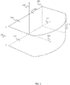
- Figure 1 illustrates an example graded-index lens 101 for focusing along multiple axes.
- the lens 101 has two opposing surfaces 111, 112, offset by a distance 132 along a first axis 121.
- the lens 101 also has a third surface 113 that is curved about the first axis 121.
- the lens 101 may be oriented such that a collection of rays of light, or a light beam, propagates through the lens 101 along a second axis 122, or the propagation axis, between the opposing surfaces 111, 112 and towards the third surface 113.
- the third surface 113 may be perpendicular to planes defined by the first surface 111 and/or the second surface 112 of the opposing surfaces 111, 112.
- the lens 101 is formed from a material having a variable refractive index along the first axis 121.
- the variable refractive index may be configured to manipulate or focus the rays of light along the first axis 121.
- the lens 101 may be composed of a substantially singular material.
- a substantially singular material may be a material of a same or similar chemical composition, but varying slightly in consistency of composition because of manufacturing errors or impurities. Further, a substantially singular material may involve a same elemental combination, but varying consistency of particular elemental constructs. Further, a substantially similar material may refer to a class of material having similar or same elemental formulation but varying compositions.
- the lens is formed from SiON having varied relative amounts of oxygen and nitrogen along the first axis 121.
- the variation of the relative amounts of oxygen and nitrogen in the material may be configured to provide a parabolic variable refractive index along the first axis.
- the variation of the relative amounts of oxygen and nitrogen in the material may be symmetric about a centerline of the lens 101, or another axis.
- the curve of the third surface 113 of the lens 101 may be configured to focus the rays of light along a third axis 123.
- the first axis 121, the second axis 122, and/or the third axis 123 may be perpendicular.
- a fourth surface 114 may also, or alternatively, be curved around the first axis 121 to focus the rays of light along the third axis 123.
- the curves of the third surface 113 and/or the fourth surface 114 may be curved in a concave or convex manner depending on the optical characteristics indicated for various embodiments.
- Figure 2A illustrates a side view of a propagation of rays of light 202 through a length 134 in a Z axis (e.g., axis 122 of Figure 1 ) of a lens 101.
- the light rays 202 enter the lens 101 at a location 212 having a trajectory in a Y axis.
- the lens 101 is composed of a material that has a variable refractive index 240 along a height 132 (e.g., axis 121 of Figure 1 ) of the lens 101 in the Y axis.
- variable refractive index 240 is configured such that the trajectory of the rays of light 202 in the Y axis changes as the rays of light 202 propagate along the length 134 of the lens 101.
- the variable refractive index 240 may vary as a parabolic function about an optical centerline of the rays of light 202.
- variable refractive index 240 may be configured to provide a focal length 136 such that the rays of light are focused in the Y axis onto an area of focus 224 on a surface 220.
- An area of focus 224, or focal area may be an area of a surface which receives a beam of light that has a certain cross sectional area.
- the beam of light may have been manipulated, for example using the lens 101, such that the rays of light included in the beam are converged, collimated, or diverged into a beam of a desired cross sectional area at the location that the surface intersects with the beam.
- the area of focus 224 may be the cross sectional area of the rays of light 202 at the distance 136 the surface 220 intersects with the rays of light 202. Further, the area of focus 224 may involve a different height and width dimension, based on characteristics of an implemented embodiment.
- the surface 220 may be an external surface of an integrated circuit board or optical coupling.
- Equation 1 n 1 is the peak refractive index of the lens, a is half the height 132 of the lens, r is a variable position along a line extending to the focal length 136, n ( r ) is the refractive index of the material between the lens and the surface 220 at position or length r, and ⁇ is the refractive difference defined using Equation 2 where n 2 is a refractive index of a second material in a propagation path, such as a cladding material.
- ⁇ n 1 2 ⁇ n 2 2 2 n 1 2
- Equation 3 the sinusoidal path length for a period, P, of light rays manipulated by a parabolic refractive index lens is given by Equation 3.
- P 2 ⁇ a ⁇ 2 ⁇ ⁇
- focal length decreases as P decreases.
- the length 136 to the surface is between 0.25 P and 0.5 P.
- Figure 2B illustrates a top view of the propagation of light rays 202 through the lens 101 of Figure 2A .
- the lens 101 has a curved surface 140 extending along a width 138 of the lens 101 in the X axis.
- the curved surface 140 is configured such that the rays of light 202 are focused in the X axis by the curved surface 140 of the lens 101 onto the area of focus 224 on the surface 220.
- the curved surface 140 may involve any radius of curvature, constant or variable along the curves length, so as to focus the rays of light 202 appropriately on the area of focus 224.
- a lens may be oriented relative to a waveguide to appropriately manipulate light rays 202 into an area of focus 224 for coupling.
- the lens may be oriented relative to the waveguide such that a light beam propagates through both the waveguide and the lens.
- the lens may be oriented and configured to focus a light beam that has propagated through the waveguide.
- the lens may involve gradient index focal properties along a first axis and focal properties produced by a curve in a surface of the lens along a second axis.
- multiple lenses and waveguides may be provided in a single component or system for multiple optical outputs and output configurations.
- Figure 3A and Figure 3B illustrate embodiments of an optical coupling involving a waveguide 320 and a lens 101.
- the optical coupling may provide a coupling between an integrated circuit and an optically conductive fiber.
- the optical coupling may involve the propagation of a light beam into the optical coupling at the waveguide 320.
- the light beam may have originated from an integrated circuit physically connected to the optical coupling at the waveguide 320.
- the light beam may propagate through the waveguide 320 and the lens 101 to project and manipulate the light beam 202 onto a focal area 224 of an external surface 220 of the optical coupling.
- the optically conductive fiber may then receive the light beam 202 at the focal area 224 on the external surface 220.
- the waveguide 320 is embedded or otherwise inserted in a substance 330, such as silicon dioxide ("Silica").
- the waveguide 320 is composed of a material suitable for propagation of light rays, which has a relative refractive index to the embedding material such that the light rays are bound within the waveguide 320.
- the waveguide may be composed of Silicon.
- the waveguide 320 is oriented a distance from the lens 101 which is constructed or composed of SiON. Both the waveguide 320 and the lens have an optical centerline, about which light rays propagate through the respective components.
- the lens 101 and the waveguide 320 have a common optical centerline 301 which provides that the light rays 202 to propagate along the common centerline 301 to the area of focus 224 on a surface 220.
- Figure 3B illustrates an embodiment that involve an offset of the waveguide optical centerline 302 and the lens optical centerline 304 such that the rays of light 202 propagate along a different axis 306 to an area of focus 224 on a surface 220.
- the location of the area of focus 224 is controlled by the offset 335 of optical centerlines. Any amount of offset may be used, resulting in any angle of deviation.
- the light beam may travel from the lens 101 to the surface 220 by propagating through an atmosphere, air, or other medium not coupled with the lens.
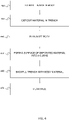
- Figure 4 is an example flowchart for an embodiment involving the formation of a multi-axis graded-index photonic coupling.
- the acts of the flowchart may be performed in the order shown, or a different order. Additional, different, or fewer acts may be provided. For example, acts 460 and/or 470 are not performed.
- a trench is formed in a body.
- the body may be any sort of body or object.
- the body may involve an optical coupling device.
- the body may be a body 502 composed of silica having an embedded silicon waveguide 505, as is illustrated in Figure 5A .
- the trench may be formed using any technique. For example, etching techniques, such as wet etching, anisotropic wet etching, and/or plasma etching may be used.
- the formed trench may be oriented such that the trench crosses a path extending longitudinally from the waveguide, as is illustrated by the trench 510 with reference to Figure 5B .
- the trench may be oriented perpendicular to a length of the waveguide.
- material may be deposited in the trench.
- the material may have a variable refractive index along the depth of the trench such that the material is configured to focus light rays propagating from the waveguide along an axis parallel to the depth of the trench.
- the trench 510 may be filled with the material 515 as is illustrated with respect to Figure 5C .
- the deposited material may be SiON.
- the material may be deposited using any technique.
- the material may be deposited using a chemical vapor deposition ("CVD") technique.
- CVD chemical vapor deposition
- layers of material may be deposited onto the surface of the body by plasma.
- the composition of the plasma material is determined by a mixture of the precursor gasses that flow into the plasma.
- the precursor gasses may contain silicon, oxygen, and nitrogen.
- Other gases may also be used.
- the relative amounts of oxygen and nitrogen may be controlled or varied during the material deposition.
- the deposition may begin with silicon and oxygen as precursor gases. As more material is deposited, increasing amounts of nitrogen gas and decreasing amounts of oxygen may be added as precursor gases.
- decreasing amounts of nitrogen gas and increasing amounts of oxygen gas may be added as precursor gases.
- the varied relative amounts of nitrogen and oxygen through the depth of the deposited material provide for the varying refractive index of the material.
- Non-symmetrical variation in the levels of gases may be used.
- the body may be planarized.
- Planarizing may involve any technique such that the surface is smoothed.
- planarizing may involve removing material so as to form a flat or planed surface 517 on the body and deposited material 515 in the trench 510 in a same plane. Etching, grinding, sawing or any other technique may be used to smooth the surface.
- a surface of the deposited material is formed into a curve.
- the curve may be formed by any technique.
- deposited material 515 may be removed to form the curved surface 530.
- Other material such as body material or deposited material on an opposing side of the curve may also be removed to further form or shape the deposited material.
- the trench 510 is formed with a curved wall.
- the curved surface of the deposited material is then formed by the depositing of material into the trench in act 430.
- the curved trench wall defines or forms the deposited material curved surface. Acts 450 and 460 are then not provided as a separate act.
- the added material 540 may backfill a void left by the removal of material in act 450 to form the curvature.
- the material added may be a same material of which the body is composed, or from which the trench 510 was formed.
- the trench 510 is formed from the removal of silicon dioxide material of a body and silicon dioxide is added to the body to backfill voids left by the removal of SiON material deposited in the trench.
- the body may be planarized.
- the body may be planarized to create a smooth surface in the body by the removal of any excess backfill material.
- the deposited material may be used to form a lens such that light rays propagating through the body may be focused by the deposited material onto a surface of the body.
- the light rays may be focused onto any surface of the body.
- the material may be configured such that the light rays are focused onto an end, top, side, or any other surface of the body.
- light rays may be focused external to the body. For example, on a surface of a different body.
- Figure 6 illustrates a top view of an embodiment involving an optical coupling 602 which includes a waveguide 605 that is tapered such that the cross sectional area of the waveguide 605 decreases along a length of the waveguide 605.
- the optical coupling 602 also includes a lens 101 configured to focus a light beam propagating from the waveguide along two axes onto an external surface 220 of the optical coupling 602.
- the lens 101 may focus light in a first axis by use of a material in the lens composition which has a variable refractive index along the first axis.
- the lens 101 may also focus light in a second axis by use of a curved surface 610 of the lens 101.
- the relative placement, characteristics, and/or configuration of the waveguide 605, lens 101, and the external surface 220 of the coupling may provide for specific optical characteristics of the optical coupling 602.
- optical centerlines of the waveguide 605 and the lens 101 may be aligned or offset to precisely determine the placement of an area of focus on the external surface 220, or other surfaces of the optical coupling 602.
- the relative distance between the lens 101 and the exterior surface 220 may determine a size of a focal area on the external surface 220.
- the material 615 between the surface 610 and the external surface 220 may be eliminated or not included in an optical coupling.
- the optical coupling 602 may exist as a stand-alone device which may be used in correlation with other devices to optically couple the devices.
- the optical coupling 602 may also be integrated as a component of a device to provide optical coupling capabilities for the device.
- the optical coupling 602 may be integrated into an integrated circuit device so as to optically couple the integrated circuit device to other devices.
- the optical coupling may be embedded or otherwise inserted into cladding material of an integrated circuit such that the external surface of the optical coupling is an external surface of the integrated circuit for coupling with an optical fiber.
- the optical coupling 602 may be constructed concurrently with the integrated circuit device such as during wafer level manufacture of the integrated circuit device.
Landscapes
- Physics & Mathematics (AREA)
- General Physics & Mathematics (AREA)
- Optics & Photonics (AREA)
- Engineering & Computer Science (AREA)
- Microelectronics & Electronic Packaging (AREA)
- Optical Couplings Of Light Guides (AREA)
- Optical Integrated Circuits (AREA)
Description
- The following disclosure generally relates to photonic or optical coupling and, more particularly, to photonic coupling using a graded index lens for focusing along multiple axes.
- Optically coupling integrated circuits with other components, such as optically conductive fibers or cabling, involves a propagation of light rays through components configured to transition the light rays from an integrated circuit to another component. The transition can cause a loss or degradation of data due to an ineffective propagation of the light rays during the transition. This degradation may cause slower or ineffective data transfers between the integrated circuit and the coupled component.
-
US2010/135615 describes an apparatus for coupling light between input and output waveguides includes a substrate, an input waveguide disposed on the substrate and comprising a first optical axis, and an output waveguide disposed on the substrate and comprising a second optical axis vertically offset from the first optical axis. -
US2003/035620 describes a 3D coupling system includes a layered structure that receives an input of a defined mode size. The layered structure includes a plurality of layers with varying indexes, and outputs a vertically mode converted beam associated with the input beam. -
US6865207 describes a semiconductor laser device with a spot-size converter includes at least a semiconductor laser region emitting light from an end facet thereof and a light waveguide region. The semiconductor laser region and the light waveguide region are integrated on a semiconductor substrate in a horizontal direction. A semiconductor layer is buried in a junction region between the semiconductor laser region and the light waveguide region. - Exemplary embodiments obtained by a method according to the claimed invention are described herein with reference to the following drawings:
-
Figure 1 illustrates an example embodiment of a graded-index lens for focusing along multiple axes. -
Figures 2A-2B illustrate an example of light rays propagating through a graded-index lens. -
Figures 3A-3B illustrate embodiments of graded-index lens coupling alignments. -
Figure 4 illustrates an example flowchart of an embodiment for creating a graded-index lens coupling device. -
Figures 5A-5F illustrate example stages of creating a graded-index coupling apparatus. -
Figure 6 illustrates an example embodiment of a coupling device implementing a graded-index lens to focus light rays in multiple axes. - In one embodiment, a lens may be provided to optically couple an integrated circuit with another component. The lens may use a material having a variable refractive index to focus rays of light along first axis and a curved surface to focus the rays of light along a second axis.
- A photonic or optical coupler may focus light in two dimensions, for example along a horizontal and vertical axis of a coupled integrated circuit or chip relative to a facet provided to attach the chip to other components. The focusing along the horizontal dimension may be accomplished by shaping a surface or facet of the chip into a cylindrical or parabolic shape, as seen from a top perspective view. The focusing along the vertical dimension may be accomplished by tailoring a refractive index profile of the lower and upper cladding layers in a coupling. Specifically, the index may be configured to follow an elliptic, spherical, aspherical, or parabolic profile as a function of a vertical position in the coupling.
- A lens may be integrated with or added to a chip to provide the coupling. Further, a lens may be constructed as a part of a complementary metal-oxide-semiconductor ("CMOS") or other micro electro-mechanical system ("MEMS") wafer level manufacturing process. For example, layers of the lens material may be added to a chip as layers during the manufacturing process. Also, multiple lenses, each potentially having different configured optical properties, may be formed in a single chip using these or similar techniques.
- A lens may be combined with a tapered waveguide to transform propagating light rays from a waveguide-bound optical mode to a fiber based optical mode. The waveguide taper may consist of a narrowing of the waveguide end in a vicinity of the lens, which causes the optical mode within the waveguide to expand in diameter as it nears the lens. A collection of light rays or a light beam emanating from the tapered waveguide may have a large aperture, meaning that the light rays are rapidly diverging in space, and thus would not efficiently couple a chip to a fiber without the aid of a lens. A configuration of the lens may provide that the light rays are transformed to less rapidly diverging light rays, to a collimated beam of light rays, or to converging light rays, thus allowing for an efficient coupling of the chip with a fiber.
- Placement and dimensions of a tapered waveguide may be selected to produce a light beam with desired properties such as a mode field diameter or numerical aperture. Further properties of the waveguide taper may be calculated using finite-difference time domain ("FDTD") simulations. Likewise, a lens focal length, size, aperture clarity or color, as well as other lens properties, may be chosen to transform a light beam emanating from the waveguide such that the light beam couples efficiently to an external fiber or other component or external fixture. Particular focal properties of the lens may be configured to focus the light beam in multiple directions using various techniques. Also, the relative placement of a waveguide and a lens may further provide for particular placement of a facet area for coupling. In an embodiment, controlling the optical centerline alignment of the lens and the waveguide may provide for particular placement of a focal area, or coupling facet, of a coupling device. For example, a light beam may propagate along a common optical centerline of a waveguide and lens that are aligned, or in-line, such that the light beam continues to propagate along the common optical centerline to an edge of the coupling providing a coupling facet area. In another example, the waveguide optical centerline and the lens optical centerline may be offset so as to angle a propagation centerline of the light beam to an area of the surface of the coupling that is not along the optical centerline of either the lens or the waveguide.
- Combinations of a lens and waveguide taper may be used to couple light beams either into or out of a chip. Particular embodiments may involve specific combinations or configurations of lens and waveguide focal properties that may be customized for varying chip, fixture, fiber, or other component configurations to provide for high coupling efficiency.
- Further, lens fabrication as a part of a wafer level controllable process may be controlled at a very high level of precision. Alignment of the lens to an on-chip waveguide may be accurate to within 200 nanometers or better using existing MEMS processing techniques. Further, the optical properties of the lens material may be tuned to specific and particular configurations in a predictable and highly repeatable manner. Also, material gaps between the chip, waveguide, and/or lens may be reduced or eliminated using wafer level techniques for lens fabrication.
- Graded-index lenses with multiple axes focal properties may be used to optically couple any photonic components. For example, such lenses may be used in optical transceiver module manufacture as well as short-distance optical interconnects such as active optical cables, board-to-board coupling, rack-to-rack coupling, or any implementation which may involve a chip-to-fiber optical coupling.
- According to the claimed invention, a trench is etched into a wafer surface, in front of an optical waveguide such as a tapered or nano-tapered waveguide. Multiple layers of dielectric material, such as silicon-oxynitride ("SiON") are deposited in the trench. A composition of the material (i.e. SiON) for each layer of the deposited material is controlled so as to form a graded index lens having a variable refractive index along an axis of the lens to control a focal height of a light beam. Such controlled chemistry or composition varies the amounts of oxygen and/or nitrogen in the material. Further, a contoured shape of a surface of the lens provides for control of a focal width. Such a surface is generated using a similarly contoured wall of the trench, or by other forming techniques. In this way, the focal length may be controlled by a combination of the contoured surface and gradient index profile of the lens.
-
Figure 1 illustrates an example graded-index lens 101 for focusing along multiple axes. Thelens 101 has twoopposing surfaces distance 132 along afirst axis 121. Thelens 101 also has athird surface 113 that is curved about thefirst axis 121. Thelens 101 may be oriented such that a collection of rays of light, or a light beam, propagates through thelens 101 along asecond axis 122, or the propagation axis, between theopposing surfaces third surface 113. In an embodiment, thethird surface 113 may be perpendicular to planes defined by thefirst surface 111 and/or thesecond surface 112 of theopposing surfaces - The
lens 101 is formed from a material having a variable refractive index along thefirst axis 121. The variable refractive index may be configured to manipulate or focus the rays of light along thefirst axis 121. In an embodiment, thelens 101 may be composed of a substantially singular material. A substantially singular material may be a material of a same or similar chemical composition, but varying slightly in consistency of composition because of manufacturing errors or impurities. Further, a substantially singular material may involve a same elemental combination, but varying consistency of particular elemental constructs. Further, a substantially similar material may refer to a class of material having similar or same elemental formulation but varying compositions. The lens is formed from SiON having varied relative amounts of oxygen and nitrogen along thefirst axis 121. The variation of the relative amounts of oxygen and nitrogen in the material may be configured to provide a parabolic variable refractive index along the first axis. In an embodiment, the variation of the relative amounts of oxygen and nitrogen in the material may be symmetric about a centerline of thelens 101, or another axis. - Also, the curve of the
third surface 113 of thelens 101 may be configured to focus the rays of light along athird axis 123. In an embodiment, thefirst axis 121, thesecond axis 122, and/or thethird axis 123 may be perpendicular. Also, afourth surface 114 may also, or alternatively, be curved around thefirst axis 121 to focus the rays of light along thethird axis 123. Further, the curves of thethird surface 113 and/or thefourth surface 114 may be curved in a concave or convex manner depending on the optical characteristics indicated for various embodiments. -
Figure 2A illustrates a side view of a propagation of rays oflight 202 through alength 134 in a Z axis (e.g.,axis 122 ofFigure 1 ) of alens 101. The light rays 202 enter thelens 101 at alocation 212 having a trajectory in a Y axis. Thelens 101 is composed of a material that has a variablerefractive index 240 along a height 132 (e.g.,axis 121 ofFigure 1 ) of thelens 101 in the Y axis. The variablerefractive index 240 is configured such that the trajectory of the rays oflight 202 in the Y axis changes as the rays oflight 202 propagate along thelength 134 of thelens 101. For example, the variablerefractive index 240 may vary as a parabolic function about an optical centerline of the rays oflight 202. - Further, the variable
refractive index 240 may be configured to provide afocal length 136 such that the rays of light are focused in the Y axis onto an area offocus 224 on asurface 220. An area offocus 224, or focal area, may be an area of a surface which receives a beam of light that has a certain cross sectional area. The beam of light may have been manipulated, for example using thelens 101, such that the rays of light included in the beam are converged, collimated, or diverged into a beam of a desired cross sectional area at the location that the surface intersects with the beam. For example, the area offocus 224 may be the cross sectional area of the rays oflight 202 at thedistance 136 thesurface 220 intersects with the rays oflight 202. Further, the area offocus 224 may involve a different height and width dimension, based on characteristics of an implemented embodiment. - In an embodiment, the
surface 220 may be an external surface of an integrated circuit board or optical coupling. For a parabolic graded index lens configuration thefocal length 136 may be determined using Equation 1.
- In Equation 1, n 1 is the peak refractive index of the lens, a is half the
height 132 of the lens, r is a variable position along a line extending to thefocal length 136, n(r) is the refractive index of the material between the lens and thesurface 220 at position or length r, and Δ is the refractive difference defined using Equation 2 where n 2 is a refractive index of a second material in a propagation path, such as a cladding material.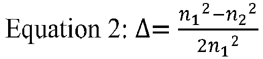
- Further, the sinusoidal path length for a period, P, of light rays manipulated by a parabolic refractive index lens is given by Equation 3.

- Therefore, focal length decreases as P decreases. In an embodiment, the
length 136 to the surface is between 0.25 P and 0.5 P. -
Figure 2B illustrates a top view of the propagation oflight rays 202 through thelens 101 ofFigure 2A . Thelens 101 has acurved surface 140 extending along awidth 138 of thelens 101 in the X axis. Thecurved surface 140 is configured such that the rays oflight 202 are focused in the X axis by thecurved surface 140 of thelens 101 onto the area offocus 224 on thesurface 220. Thecurved surface 140 may involve any radius of curvature, constant or variable along the curves length, so as to focus the rays oflight 202 appropriately on the area offocus 224. - In an embodiment involving a light ray coupler, a lens may be oriented relative to a waveguide to appropriately manipulate
light rays 202 into an area offocus 224 for coupling. The lens may be oriented relative to the waveguide such that a light beam propagates through both the waveguide and the lens. Specifically, the lens may be oriented and configured to focus a light beam that has propagated through the waveguide. For example, the lens may involve gradient index focal properties along a first axis and focal properties produced by a curve in a surface of the lens along a second axis. Further, multiple lenses and waveguides may be provided in a single component or system for multiple optical outputs and output configurations. -
Figure 3A and Figure 3B illustrate embodiments of an optical coupling involving awaveguide 320 and alens 101. The optical coupling may provide a coupling between an integrated circuit and an optically conductive fiber. For example, the optical coupling may involve the propagation of a light beam into the optical coupling at thewaveguide 320. The light beam may have originated from an integrated circuit physically connected to the optical coupling at thewaveguide 320. The light beam may propagate through thewaveguide 320 and thelens 101 to project and manipulate thelight beam 202 onto afocal area 224 of anexternal surface 220 of the optical coupling. The optically conductive fiber may then receive thelight beam 202 at thefocal area 224 on theexternal surface 220. - In the embodiment of
Figure 3A , thewaveguide 320 is embedded or otherwise inserted in asubstance 330, such as silicon dioxide ("Silica"). Thewaveguide 320 is composed of a material suitable for propagation of light rays, which has a relative refractive index to the embedding material such that the light rays are bound within thewaveguide 320. For example, the waveguide may be composed of Silicon. Thewaveguide 320 is oriented a distance from thelens 101 which is constructed or composed of SiON. Both thewaveguide 320 and the lens have an optical centerline, about which light rays propagate through the respective components. InFigure 3A , thelens 101 and thewaveguide 320 have a commonoptical centerline 301 which provides that thelight rays 202 to propagate along thecommon centerline 301 to the area offocus 224 on asurface 220.Figure 3B illustrates an embodiment that involve an offset of the waveguideoptical centerline 302 and the lensoptical centerline 304 such that the rays oflight 202 propagate along adifferent axis 306 to an area offocus 224 on asurface 220. In this embodiment, the location of the area offocus 224 is controlled by the offset 335 of optical centerlines. Any amount of offset may be used, resulting in any angle of deviation. Further, the light beam may travel from thelens 101 to thesurface 220 by propagating through an atmosphere, air, or other medium not coupled with the lens. -
Figure 4 is an example flowchart for an embodiment involving the formation of a multi-axis graded-index photonic coupling. The acts of the flowchart may be performed in the order shown, or a different order. Additional, different, or fewer acts may be provided. For example, acts 460 and/or 470 are not performed. - In
act 420, a trench is formed in a body. The body may be any sort of body or object. In an embodiment, the body may involve an optical coupling device. For example, the body may be abody 502 composed of silica having an embeddedsilicon waveguide 505, as is illustrated inFigure 5A . - The trench may be formed using any technique. For example, etching techniques, such as wet etching, anisotropic wet etching, and/or plasma etching may be used. The formed trench may be oriented such that the trench crosses a path extending longitudinally from the waveguide, as is illustrated by the
trench 510 with reference toFigure 5B . In an embodiment, the trench may be oriented perpendicular to a length of the waveguide. - In
act 430, material may be deposited in the trench. The material may have a variable refractive index along the depth of the trench such that the material is configured to focus light rays propagating from the waveguide along an axis parallel to the depth of the trench. For example, thetrench 510 may be filled with the material 515 as is illustrated with respect toFigure 5C . In an embodiment, the deposited material may be SiON. - The material may be deposited using any technique. For example, the material may be deposited using a chemical vapor deposition ("CVD") technique. Using a CVD technique, layers of material may be deposited onto the surface of the body by plasma. The composition of the plasma material is determined by a mixture of the precursor gasses that flow into the plasma. In an embodiment involving SiON, the precursor gasses may contain silicon, oxygen, and nitrogen. Other gases may also be used. To form a graded index material, the relative amounts of oxygen and nitrogen may be controlled or varied during the material deposition. For example, the deposition may begin with silicon and oxygen as precursor gases. As more material is deposited, increasing amounts of nitrogen gas and decreasing amounts of oxygen may be added as precursor gases. Once half the desired depth of the deposited material is reached, decreasing amounts of nitrogen gas and increasing amounts of oxygen gas may be added as precursor gases. The varied relative amounts of nitrogen and oxygen through the depth of the deposited material provide for the varying refractive index of the material. Non-symmetrical variation in the levels of gases may be used.
- In
act 440, the body may be planarized. Planarizing may involve any technique such that the surface is smoothed. For example, with reference toFigure 5D , planarizing may involve removing material so as to form a flat or planedsurface 517 on the body and depositedmaterial 515 in thetrench 510 in a same plane. Etching, grinding, sawing or any other technique may be used to smooth the surface. - In
act 450, a surface of the deposited material is formed into a curve. The curve may be formed by any technique. In an embodiment, as represented inFigure 5E , depositedmaterial 515 may be removed to form thecurved surface 530. Other material such as body material or deposited material on an opposing side of the curve may also be removed to further form or shape the deposited material. - In another embodiment, the
trench 510 is formed with a curved wall. The curved surface of the deposited material is then formed by the depositing of material into the trench inact 430. As such, the curved trench wall defines or forms the deposited material curved surface.Acts - In
act 460, material is added to the body. With reference toFigure 5F , the addedmaterial 540 may backfill a void left by the removal of material inact 450 to form the curvature. The material added may be a same material of which the body is composed, or from which thetrench 510 was formed. In an embodiment, thetrench 510 is formed from the removal of silicon dioxide material of a body and silicon dioxide is added to the body to backfill voids left by the removal of SiON material deposited in the trench. - In
act 470, the body may be planarized. The body may be planarized to create a smooth surface in the body by the removal of any excess backfill material. - In an embodiment, the deposited material may be used to form a lens such that light rays propagating through the body may be focused by the deposited material onto a surface of the body. The light rays may be focused onto any surface of the body. For example, the material may be configured such that the light rays are focused onto an end, top, side, or any other surface of the body. In an embodiment, light rays may be focused external to the body. For example, on a surface of a different body.
-
Figure 6 illustrates a top view of an embodiment involving anoptical coupling 602 which includes awaveguide 605 that is tapered such that the cross sectional area of thewaveguide 605 decreases along a length of thewaveguide 605. Theoptical coupling 602 also includes alens 101 configured to focus a light beam propagating from the waveguide along two axes onto anexternal surface 220 of theoptical coupling 602. Thelens 101 may focus light in a first axis by use of a material in the lens composition which has a variable refractive index along the first axis. Thelens 101 may also focus light in a second axis by use of acurved surface 610 of thelens 101. Further, the relative placement, characteristics, and/or configuration of thewaveguide 605,lens 101, and theexternal surface 220 of the coupling may provide for specific optical characteristics of theoptical coupling 602. For example, optical centerlines of thewaveguide 605 and thelens 101 may be aligned or offset to precisely determine the placement of an area of focus on theexternal surface 220, or other surfaces of theoptical coupling 602. In another example, the relative distance between thelens 101 and theexterior surface 220 may determine a size of a focal area on theexternal surface 220. In an embodiment, thematerial 615 between thesurface 610 and theexternal surface 220 may be eliminated or not included in an optical coupling. - The
optical coupling 602 may exist as a stand-alone device which may be used in correlation with other devices to optically couple the devices. Theoptical coupling 602 may also be integrated as a component of a device to provide optical coupling capabilities for the device. For example, theoptical coupling 602 may be integrated into an integrated circuit device so as to optically couple the integrated circuit device to other devices. For example, the optical coupling may be embedded or otherwise inserted into cladding material of an integrated circuit such that the external surface of the optical coupling is an external surface of the integrated circuit for coupling with an optical fiber. Further, theoptical coupling 602 may be constructed concurrently with the integrated circuit device such as during wafer level manufacture of the integrated circuit device. - The illustrations of the embodiments described herein are intended to provide a general understanding of the structure of the various embodiments. The illustrations are not intended to serve as a complete description of all of the elements and features of apparatus and systems that utilize the structures or methods described herein. Many other embodiments may be apparent to those of skill in the art upon reviewing the disclosure. Other embodiments may be utilized and derived from the disclosure, such that structural and logical substitutions and changes may be made without departing from the scope of the disclosure. Additionally, the illustrations are merely representational and may not be drawn to scale. Certain proportions within the illustrations may be exaggerated, while other proportions may be minimized. Accordingly, the disclosure and the figures are to be regarded as illustrative rather than restrictive.
- While operations are depicted in the drawings and described herein in a particular order, this should not be understood as requiring that such operations be performed in the particular order shown or in sequential order, or that all illustrated operations be performed, to achieve desirable results. In certain circumstances, multitasking may be advantageous. Moreover, the separation of various system components in the embodiments described above should not be understood as requiring such separation in all embodiments
- It is therefore intended that the foregoing detailed description be regarded as illustrative rather than limiting, and that it be understood that it is the following claims, that are intended to define the scope of this invention.
Claims (5)
- A method comprising:etching (420) a trench in a body, the body having an embedded waveguide (605);depositing (430) a material in the trench having a variable refractive index along a depth of the trench, the variable refractive index configured to focus light rays propagating from the waveguide along an axis parallel to the depth of the trench onto an area (220) of a surface of the body, wherein the material in the trench is Silicon-Oxynitride, SiON, and wherein the relative amounts of Oxygen and Nitrogen in the material vary along the axis parallel to the depth of the trench; andforming (450) a surface of the material in the trench into a curve (610), the curve (610) configured to focus the light rays along an axis parallel to a length of the trench onto the area (220) of the surface of the body,wherein the trench further comprises a curved surface, and wherein forming the surface of the material into a curve comprises filling the trench with the material such that the curve (610) in the surface of the material is formed by the curved surface of the trench.
- The method of claim 1, further comprising:
planarizing (440) the body after depositing the material in the trench. - The method of claim 1, further comprising:removing deposited material from parallel surfaces of the body; andfilling (460) vacancies left by the removing with a material different from the material of the deposited material, optionally wherein the surface of the material in the trench is formed into a curve by the removing of the deposited material.
- The method of claim 1, wherein an optical centerline of the waveguide (605) and an optical centerline of the material deposited in the trench are aligned in an axis parallel to the depth of the trench or wherein an optical centerline of the waveguide (605) and an optical centerline of the material deposited in the trench are offset in an axis parallel to the depth of the trench.
- The method of any of the previous claims wherein the material in the trench is deposited using chemical vapor deposition.
Applications Claiming Priority (2)
| Application Number | Priority Date | Filing Date | Title |
|---|---|---|---|
| US14/330,487 US9411105B2 (en) | 2014-07-14 | 2014-07-14 | Multi-axis graded-index photonic coupling |
| PCT/US2015/033891 WO2016010641A1 (en) | 2014-07-14 | 2015-06-03 | Multi-axis graded-index photonic coupling |
Publications (2)
| Publication Number | Publication Date |
|---|---|
| EP3170042A1 EP3170042A1 (en) | 2017-05-24 |
| EP3170042B1 true EP3170042B1 (en) | 2022-09-14 |
Family
ID=53398237
Family Applications (1)
| Application Number | Title | Priority Date | Filing Date |
|---|---|---|---|
| EP15729031.3A Active EP3170042B1 (en) | 2014-07-14 | 2015-06-03 | Method of obtaining a multi-axis graded-index photonic coupling |
Country Status (4)
| Country | Link |
|---|---|
| US (2) | US9411105B2 (en) |
| EP (1) | EP3170042B1 (en) |
| CN (1) | CN106537192B (en) |
| WO (1) | WO2016010641A1 (en) |
Families Citing this family (16)
| Publication number | Priority date | Publication date | Assignee | Title |
|---|---|---|---|---|
| CN107530034A (en) | 2015-03-16 | 2018-01-02 | 奇跃公司 | Augmented reality pulse oximetry |
| WO2016196035A1 (en) * | 2015-05-29 | 2016-12-08 | Corning Optical Communications LLC | Planar tapered waveguide coupling elements and optical couplings for photonic circuits |
| US10539744B2 (en) * | 2016-01-14 | 2020-01-21 | Futurewei Technologies, Inc. | Gapless optical mode converter |
| EP4273615B1 (en) | 2016-04-08 | 2025-11-12 | Magic Leap, Inc. | Augmented reality systems and methods with variable focus lens elements |
| FR3061561B1 (en) | 2016-12-29 | 2019-05-31 | Commissariat A L'energie Atomique Et Aux Energies Alternatives | COLLIMATION DEVICE |
| KR102601052B1 (en) | 2017-02-23 | 2023-11-09 | 매직 립, 인코포레이티드 | Display system with variable power reflector |
| US10473857B2 (en) * | 2017-07-11 | 2019-11-12 | Mellanox Technologies, Ltd. | Gradient-index waveguide lateral coupler having an active region with an index of refraction that is non-constant laterally |
| US10705313B2 (en) | 2018-02-23 | 2020-07-07 | Cisco Technology, Inc. | Optical fiber coupling using multiple cylindrical lenses |
| US10481355B2 (en) | 2018-04-20 | 2019-11-19 | Sicoya Gmbh | Optical assembly |
| WO2019246594A1 (en) | 2018-06-22 | 2019-12-26 | Masseta Technologies Llc | Discrete optical unit on a substrate of an integrated photonics chip |
| KR102889540B1 (en) | 2020-10-23 | 2025-11-24 | 애플 인크. | Fast-axis collimator with hanging connector |
| CN112649903B (en) | 2020-12-28 | 2022-07-01 | 厦门天马微电子有限公司 | Composite film group, preparation method thereof, lighting device and display device |
| US20230087293A1 (en) * | 2021-09-23 | 2023-03-23 | Apple Inc. | Light Output Devices and Light Outputting Methods for Optical Systems |
| KR20240043812A (en) * | 2021-09-23 | 2024-04-03 | 애플 인크. | Light output devices and light output methods for optical systems |
| US12292597B2 (en) * | 2021-09-23 | 2025-05-06 | Apple Inc. | Light output devices and light outputting methods for optical systems |
| CN114217380B (en) * | 2021-12-17 | 2024-04-02 | 武汉光谷信息光电子创新中心有限公司 | End face coupler and preparation method thereof |
Citations (1)
| Publication number | Priority date | Publication date | Assignee | Title |
|---|---|---|---|---|
| US6865207B1 (en) * | 1998-12-18 | 2005-03-08 | Sharp Kabushiki Kaisha | Semiconductor laser device withspot-size converter and method for fabricating the same |
Family Cites Families (40)
| Publication number | Priority date | Publication date | Assignee | Title |
|---|---|---|---|---|
| JPS60114811A (en) | 1983-11-28 | 1985-06-21 | Hitachi Ltd | Optical waveguide and its production |
| US4770506A (en) * | 1983-12-28 | 1988-09-13 | Canon Kabushiki Kaisha | Gradient index single lens |
| US4762403A (en) * | 1984-04-13 | 1988-08-09 | Canon Kabushiki Kaisha | Imaging optical system having a distributed index lens |
| JPH0711630B2 (en) * | 1985-08-07 | 1995-02-08 | オリンパス光学工業株式会社 | Microscope objective lens |
| US4907864A (en) * | 1987-08-19 | 1990-03-13 | John E. Fetzer Foundation | Macro-gradient optical density transmissive light concentrators, lenses and compound lenses of large geometry |
| US4900138A (en) * | 1988-07-01 | 1990-02-13 | Gradient Lens Corporation | Composite gradient index and curved surface anamorphic lens and applications |
| US5044737A (en) * | 1989-07-13 | 1991-09-03 | Isotec Partners, Limited | Double axial gradient lens and process for fabrication thereof |
| JP2597513B2 (en) * | 1989-12-19 | 1997-04-09 | オリンパス光学工業株式会社 | Microscope objective lens |
| US5236486A (en) * | 1991-10-24 | 1993-08-17 | Lightpath Technologies, Inc. | Shaped gradient fabrication in lenses by molding from axial gradient |
| US6092728A (en) * | 1992-03-30 | 2000-07-25 | Symbol Technologies, Inc. | Miniature laser diode focusing module using micro-optics |
| US5579168A (en) * | 1993-12-22 | 1996-11-26 | Nikon Corporation | Zoom lens system with gradient index lens |
| US5871266A (en) * | 1995-06-26 | 1999-02-16 | Nissho Giken Kabushiki Kaisha | Projection-type display device |
| JP3585297B2 (en) * | 1995-09-12 | 2004-11-04 | オリンパス株式会社 | Objective lens |
| US5995295A (en) * | 1995-12-13 | 1999-11-30 | Olympus Optical Co., Ltd. | Lens system |
| US6016224A (en) * | 1995-12-18 | 2000-01-18 | Olympus Optical Co., Ltd. | Multiple image optics system |
| EP0916107B1 (en) * | 1996-07-28 | 2004-02-11 | Karl Storz GmbH & Co. KG | Endoscope with at least one reversal system with a non-homogeneous refraction index |
| US7164818B2 (en) * | 2001-05-03 | 2007-01-16 | Neophontonics Corporation | Integrated gradient index lenses |
| US20020150333A1 (en) * | 2001-02-17 | 2002-10-17 | Reed William Alfred | Fiber devices using grin fiber lenses |
| US6768844B2 (en) * | 2001-03-30 | 2004-07-27 | Raytheon Company | Method and apparatus for effecting alignment in an optical apparatus |
| EP1419407A4 (en) * | 2001-07-24 | 2005-11-09 | Tyco Electronics Corp | Expanded beam connector system |
| WO2003014785A1 (en) * | 2001-08-07 | 2003-02-20 | Massachusetts Institute Of Technology | Compact three-dimensional mode size converters for fiber-waveguide coupling |
| US6676302B2 (en) * | 2001-09-17 | 2004-01-13 | Stratos Lightwave, Inc. | Method of constructing a fiber optics communications module |
| US6927927B2 (en) * | 2001-11-27 | 2005-08-09 | Minolta Co., Ltd. | Taking lens system |
| US6789931B2 (en) * | 2002-01-30 | 2004-09-14 | Christie Digital Systems Inc. | Intense brightness optical system |
| US6963682B2 (en) * | 2002-03-04 | 2005-11-08 | Corning Incorporated | Beam altering fiber lens device and method of manufacture |
| JP4103475B2 (en) * | 2002-07-05 | 2008-06-18 | コニカミノルタオプト株式会社 | Imaging lens device |
| US8971679B2 (en) * | 2002-08-28 | 2015-03-03 | Optonet Inc. | Apparatus and method for passive alignment of optical devices |
| US8538208B2 (en) * | 2002-08-28 | 2013-09-17 | Seng-Tiong Ho | Apparatus for coupling light between input and output waveguides |
| US7643719B1 (en) * | 2003-03-14 | 2010-01-05 | Phosistor Technologies, Inc. | Superlens and a method for making the same |
| JP3896988B2 (en) * | 2003-05-12 | 2007-03-22 | コニカミノルタフォトイメージング株式会社 | Imaging lens device |
| JP3750672B2 (en) * | 2003-05-20 | 2006-03-01 | コニカミノルタフォトイメージング株式会社 | Imaging lens device |
| JP4569155B2 (en) * | 2004-04-20 | 2010-10-27 | コニカミノルタオプト株式会社 | Magnification optical system, imaging lens device, and digital device |
| US7619807B2 (en) * | 2004-11-08 | 2009-11-17 | Angstrom, Inc. | Micromirror array lens with optical surface profiles |
| CN100456581C (en) * | 2006-10-12 | 2009-01-28 | 飞秒光电科技(西安)有限公司 | Semiconductor laser shaper |
| US20100238400A1 (en) * | 2006-10-25 | 2010-09-23 | Volk Donald A | Multi-layered gradient index progressive lens |
| US7740354B2 (en) * | 2006-10-25 | 2010-06-22 | Volk Donald A | Multi-layered gradient index progressive lens |
| US8259155B2 (en) * | 2007-12-05 | 2012-09-04 | Cisco Technology, Inc. | Providing perspective-dependent views to video conference participants |
| WO2011163559A1 (en) * | 2010-06-25 | 2011-12-29 | Elenza, Inc. | Implantable ophthalmic devices with circularly asymmetric optic and methods |
| US9557488B2 (en) * | 2011-01-11 | 2017-01-31 | Corning Incorporated | Optical connector with lenses having opposing angled planar surfaces |
| US9213175B2 (en) * | 2011-10-28 | 2015-12-15 | Craig B. Arnold | Microscope with tunable acoustic gradient index of refraction lens enabling multiple focal plan imaging |
-
2014
- 2014-07-14 US US14/330,487 patent/US9411105B2/en active Active
-
2015
- 2015-06-03 EP EP15729031.3A patent/EP3170042B1/en active Active
- 2015-06-03 WO PCT/US2015/033891 patent/WO2016010641A1/en not_active Ceased
- 2015-06-03 CN CN201580038702.1A patent/CN106537192B/en active Active
-
2016
- 2016-07-11 US US15/206,752 patent/US9784920B2/en active Active
Patent Citations (1)
| Publication number | Priority date | Publication date | Assignee | Title |
|---|---|---|---|---|
| US6865207B1 (en) * | 1998-12-18 | 2005-03-08 | Sharp Kabushiki Kaisha | Semiconductor laser device withspot-size converter and method for fabricating the same |
Also Published As
| Publication number | Publication date |
|---|---|
| CN106537192B (en) | 2019-03-22 |
| EP3170042A1 (en) | 2017-05-24 |
| US20160011375A1 (en) | 2016-01-14 |
| US9411105B2 (en) | 2016-08-09 |
| US9784920B2 (en) | 2017-10-10 |
| WO2016010641A1 (en) | 2016-01-21 |
| US20160320563A1 (en) | 2016-11-03 |
| CN106537192A (en) | 2017-03-22 |
Similar Documents
| Publication | Publication Date | Title |
|---|---|---|
| US9784920B2 (en) | Multi-axis graded-index photonic coupling | |
| US9784930B2 (en) | Optical interface device having a curved waveguide using laser writing and methods of forming | |
| Djogo et al. | Femtosecond laser additive and subtractive micro-processing: enabling a high-channel-density silica interposer for multicore fibre to silicon-photonic packaging | |
| US9122037B2 (en) | Coupling system for optical fibers and optical waveguides | |
| US7228032B2 (en) | Apparatus and methods for launching an optical signal into multimode optical fiber | |
| US8971679B2 (en) | Apparatus and method for passive alignment of optical devices | |
| EP3296783B1 (en) | Integrated photonics waveguide grating coupler | |
| US8538208B2 (en) | Apparatus for coupling light between input and output waveguides | |
| US10295750B2 (en) | Horizontal coupling to silicon waveguides | |
| US9746620B2 (en) | Expanded beam connector, optical cable assembly, and method of manufacturing | |
| CN104797963A (en) | Optical photonic circuit coupling | |
| US10310195B2 (en) | Adiabatic optical coupling systems | |
| US20160062039A1 (en) | Mode size converters and optical assemblies | |
| WO2017054683A1 (en) | Optical coupling adaptor for optical signal coupling between photonic integrated circuit and optical fiber | |
| US9329335B2 (en) | Broadband multi-mode optical fibers with flat-zone in dopant concentration profile | |
| US11828981B2 (en) | Optical device with graded index planar lens | |
| Li et al. | Novel three-dimensional 90 bend waveguides with high optical transmission efficiency based on silicon-on-insulator | |
| Shiraishi et al. | High focusing power lensed fibers employing graded-index fiber with eigen-beam diameter | |
| WO2023275531A1 (en) | Optical fiber positioning apparatus | |
| Montalbo | Fiber to waveguide couplers for silicon photonics | |
| Yamasaki et al. | Spot size converter with cross-vertical taper for low-loss coupling between ZrO 2-SiO 2 PLC and SMF | |
| Yang et al. | Critical dimensions of directional couplers |
Legal Events
| Date | Code | Title | Description |
|---|---|---|---|
| STAA | Information on the status of an ep patent application or granted ep patent |
Free format text: STATUS: THE INTERNATIONAL PUBLICATION HAS BEEN MADE |
|
| PUAI | Public reference made under article 153(3) epc to a published international application that has entered the european phase |
Free format text: ORIGINAL CODE: 0009012 |
|
| STAA | Information on the status of an ep patent application or granted ep patent |
Free format text: STATUS: REQUEST FOR EXAMINATION WAS MADE |
|
| 17P | Request for examination filed |
Effective date: 20161220 |
|
| AK | Designated contracting states |
Kind code of ref document: A1 Designated state(s): AL AT BE BG CH CY CZ DE DK EE ES FI FR GB GR HR HU IE IS IT LI LT LU LV MC MK MT NL NO PL PT RO RS SE SI SK SM TR |
|
| AX | Request for extension of the european patent |
Extension state: BA ME |
|
| DAV | Request for validation of the european patent (deleted) | ||
| DAX | Request for extension of the european patent (deleted) | ||
| STAA | Information on the status of an ep patent application or granted ep patent |
Free format text: STATUS: EXAMINATION IS IN PROGRESS |
|
| 17Q | First examination report despatched |
Effective date: 20200508 |
|
| GRAP | Despatch of communication of intention to grant a patent |
Free format text: ORIGINAL CODE: EPIDOSNIGR1 |
|
| RIC1 | Information provided on ipc code assigned before grant |
Ipc: G02B 6/42 20060101ALN20220304BHEP Ipc: G02B 6/30 20060101ALN20220304BHEP Ipc: G02B 6/12 20060101ALN20220304BHEP Ipc: G02B 3/00 20060101ALI20220304BHEP Ipc: G02B 6/124 20060101AFI20220304BHEP |
|
| STAA | Information on the status of an ep patent application or granted ep patent |
Free format text: STATUS: GRANT OF PATENT IS INTENDED |
|
| RIC1 | Information provided on ipc code assigned before grant |
Ipc: G02B 6/42 20060101ALN20220328BHEP Ipc: G02B 6/30 20060101ALN20220328BHEP Ipc: G02B 6/12 20060101ALN20220328BHEP Ipc: G02B 3/00 20060101ALI20220328BHEP Ipc: G02B 6/124 20060101AFI20220328BHEP |
|
| INTG | Intention to grant announced |
Effective date: 20220414 |
|
| RIC1 | Information provided on ipc code assigned before grant |
Ipc: G02B 6/42 20060101ALN20220406BHEP Ipc: G02B 6/30 20060101ALN20220406BHEP Ipc: G02B 6/12 20060101ALN20220406BHEP Ipc: G02B 3/00 20060101ALI20220406BHEP Ipc: G02B 6/124 20060101AFI20220406BHEP |
|
| GRAS | Grant fee paid |
Free format text: ORIGINAL CODE: EPIDOSNIGR3 |
|
| GRAA | (expected) grant |
Free format text: ORIGINAL CODE: 0009210 |
|
| STAA | Information on the status of an ep patent application or granted ep patent |
Free format text: STATUS: THE PATENT HAS BEEN GRANTED |
|
| AK | Designated contracting states |
Kind code of ref document: B1 Designated state(s): AL AT BE BG CH CY CZ DE DK EE ES FI FR GB GR HR HU IE IS IT LI LT LU LV MC MK MT NL NO PL PT RO RS SE SI SK SM TR |
|
| REG | Reference to a national code |
Ref country code: GB Ref legal event code: FG4D |
|
| REG | Reference to a national code |
Ref country code: CH Ref legal event code: EP |
|
| REG | Reference to a national code |
Ref country code: DE Ref legal event code: R096 Ref document number: 602015080795 Country of ref document: DE |
|
| REG | Reference to a national code |
Ref country code: IE Ref legal event code: FG4D |
|
| REG | Reference to a national code |
Ref country code: AT Ref legal event code: REF Ref document number: 1519045 Country of ref document: AT Kind code of ref document: T Effective date: 20221015 |
|
| REG | Reference to a national code |
Ref country code: LT Ref legal event code: MG9D |
|
| REG | Reference to a national code |
Ref country code: NL Ref legal event code: MP Effective date: 20220914 |
|
| PG25 | Lapsed in a contracting state [announced via postgrant information from national office to epo] |
Ref country code: SE Free format text: LAPSE BECAUSE OF FAILURE TO SUBMIT A TRANSLATION OF THE DESCRIPTION OR TO PAY THE FEE WITHIN THE PRESCRIBED TIME-LIMIT Effective date: 20220914 Ref country code: RS Free format text: LAPSE BECAUSE OF FAILURE TO SUBMIT A TRANSLATION OF THE DESCRIPTION OR TO PAY THE FEE WITHIN THE PRESCRIBED TIME-LIMIT Effective date: 20220914 Ref country code: NO Free format text: LAPSE BECAUSE OF FAILURE TO SUBMIT A TRANSLATION OF THE DESCRIPTION OR TO PAY THE FEE WITHIN THE PRESCRIBED TIME-LIMIT Effective date: 20221214 Ref country code: LV Free format text: LAPSE BECAUSE OF FAILURE TO SUBMIT A TRANSLATION OF THE DESCRIPTION OR TO PAY THE FEE WITHIN THE PRESCRIBED TIME-LIMIT Effective date: 20220914 Ref country code: LT Free format text: LAPSE BECAUSE OF FAILURE TO SUBMIT A TRANSLATION OF THE DESCRIPTION OR TO PAY THE FEE WITHIN THE PRESCRIBED TIME-LIMIT Effective date: 20220914 Ref country code: FI Free format text: LAPSE BECAUSE OF FAILURE TO SUBMIT A TRANSLATION OF THE DESCRIPTION OR TO PAY THE FEE WITHIN THE PRESCRIBED TIME-LIMIT Effective date: 20220914 |
|
| REG | Reference to a national code |
Ref country code: AT Ref legal event code: MK05 Ref document number: 1519045 Country of ref document: AT Kind code of ref document: T Effective date: 20220914 |
|
| PG25 | Lapsed in a contracting state [announced via postgrant information from national office to epo] |
Ref country code: HR Free format text: LAPSE BECAUSE OF FAILURE TO SUBMIT A TRANSLATION OF THE DESCRIPTION OR TO PAY THE FEE WITHIN THE PRESCRIBED TIME-LIMIT Effective date: 20220914 Ref country code: GR Free format text: LAPSE BECAUSE OF FAILURE TO SUBMIT A TRANSLATION OF THE DESCRIPTION OR TO PAY THE FEE WITHIN THE PRESCRIBED TIME-LIMIT Effective date: 20221215 |
|
| PG25 | Lapsed in a contracting state [announced via postgrant information from national office to epo] |
Ref country code: SM Free format text: LAPSE BECAUSE OF FAILURE TO SUBMIT A TRANSLATION OF THE DESCRIPTION OR TO PAY THE FEE WITHIN THE PRESCRIBED TIME-LIMIT Effective date: 20220914 Ref country code: RO Free format text: LAPSE BECAUSE OF FAILURE TO SUBMIT A TRANSLATION OF THE DESCRIPTION OR TO PAY THE FEE WITHIN THE PRESCRIBED TIME-LIMIT Effective date: 20220914 Ref country code: PT Free format text: LAPSE BECAUSE OF FAILURE TO SUBMIT A TRANSLATION OF THE DESCRIPTION OR TO PAY THE FEE WITHIN THE PRESCRIBED TIME-LIMIT Effective date: 20230116 Ref country code: ES Free format text: LAPSE BECAUSE OF FAILURE TO SUBMIT A TRANSLATION OF THE DESCRIPTION OR TO PAY THE FEE WITHIN THE PRESCRIBED TIME-LIMIT Effective date: 20220914 Ref country code: CZ Free format text: LAPSE BECAUSE OF FAILURE TO SUBMIT A TRANSLATION OF THE DESCRIPTION OR TO PAY THE FEE WITHIN THE PRESCRIBED TIME-LIMIT Effective date: 20220914 Ref country code: AT Free format text: LAPSE BECAUSE OF FAILURE TO SUBMIT A TRANSLATION OF THE DESCRIPTION OR TO PAY THE FEE WITHIN THE PRESCRIBED TIME-LIMIT Effective date: 20220914 |
|
| PG25 | Lapsed in a contracting state [announced via postgrant information from national office to epo] |
Ref country code: SK Free format text: LAPSE BECAUSE OF FAILURE TO SUBMIT A TRANSLATION OF THE DESCRIPTION OR TO PAY THE FEE WITHIN THE PRESCRIBED TIME-LIMIT Effective date: 20220914 Ref country code: PL Free format text: LAPSE BECAUSE OF FAILURE TO SUBMIT A TRANSLATION OF THE DESCRIPTION OR TO PAY THE FEE WITHIN THE PRESCRIBED TIME-LIMIT Effective date: 20220914 Ref country code: IS Free format text: LAPSE BECAUSE OF FAILURE TO SUBMIT A TRANSLATION OF THE DESCRIPTION OR TO PAY THE FEE WITHIN THE PRESCRIBED TIME-LIMIT Effective date: 20230114 Ref country code: EE Free format text: LAPSE BECAUSE OF FAILURE TO SUBMIT A TRANSLATION OF THE DESCRIPTION OR TO PAY THE FEE WITHIN THE PRESCRIBED TIME-LIMIT Effective date: 20220914 |
|
| REG | Reference to a national code |
Ref country code: DE Ref legal event code: R097 Ref document number: 602015080795 Country of ref document: DE |
|
| PG25 | Lapsed in a contracting state [announced via postgrant information from national office to epo] |
Ref country code: NL Free format text: LAPSE BECAUSE OF FAILURE TO SUBMIT A TRANSLATION OF THE DESCRIPTION OR TO PAY THE FEE WITHIN THE PRESCRIBED TIME-LIMIT Effective date: 20220914 Ref country code: AL Free format text: LAPSE BECAUSE OF FAILURE TO SUBMIT A TRANSLATION OF THE DESCRIPTION OR TO PAY THE FEE WITHIN THE PRESCRIBED TIME-LIMIT Effective date: 20220914 |
|
| P01 | Opt-out of the competence of the unified patent court (upc) registered |
Effective date: 20230525 |
|
| PLBE | No opposition filed within time limit |
Free format text: ORIGINAL CODE: 0009261 |
|
| STAA | Information on the status of an ep patent application or granted ep patent |
Free format text: STATUS: NO OPPOSITION FILED WITHIN TIME LIMIT |
|
| PG25 | Lapsed in a contracting state [announced via postgrant information from national office to epo] |
Ref country code: DK Free format text: LAPSE BECAUSE OF FAILURE TO SUBMIT A TRANSLATION OF THE DESCRIPTION OR TO PAY THE FEE WITHIN THE PRESCRIBED TIME-LIMIT Effective date: 20220914 |
|
| 26N | No opposition filed |
Effective date: 20230615 |
|
| PG25 | Lapsed in a contracting state [announced via postgrant information from national office to epo] |
Ref country code: SI Free format text: LAPSE BECAUSE OF FAILURE TO SUBMIT A TRANSLATION OF THE DESCRIPTION OR TO PAY THE FEE WITHIN THE PRESCRIBED TIME-LIMIT Effective date: 20220914 |
|
| PG25 | Lapsed in a contracting state [announced via postgrant information from national office to epo] |
Ref country code: MC Free format text: LAPSE BECAUSE OF FAILURE TO SUBMIT A TRANSLATION OF THE DESCRIPTION OR TO PAY THE FEE WITHIN THE PRESCRIBED TIME-LIMIT Effective date: 20220914 |
|
| PG25 | Lapsed in a contracting state [announced via postgrant information from national office to epo] |
Ref country code: MC Free format text: LAPSE BECAUSE OF FAILURE TO SUBMIT A TRANSLATION OF THE DESCRIPTION OR TO PAY THE FEE WITHIN THE PRESCRIBED TIME-LIMIT Effective date: 20220914 |
|
| REG | Reference to a national code |
Ref country code: CH Ref legal event code: PL |
|
| REG | Reference to a national code |
Ref country code: BE Ref legal event code: MM Effective date: 20230630 |
|
| PG25 | Lapsed in a contracting state [announced via postgrant information from national office to epo] |
Ref country code: LU Free format text: LAPSE BECAUSE OF NON-PAYMENT OF DUE FEES Effective date: 20230603 |
|
| REG | Reference to a national code |
Ref country code: IE Ref legal event code: MM4A |
|
| PG25 | Lapsed in a contracting state [announced via postgrant information from national office to epo] |
Ref country code: LU Free format text: LAPSE BECAUSE OF NON-PAYMENT OF DUE FEES Effective date: 20230603 |
|
| PG25 | Lapsed in a contracting state [announced via postgrant information from national office to epo] |
Ref country code: IE Free format text: LAPSE BECAUSE OF NON-PAYMENT OF DUE FEES Effective date: 20230603 |
|
| PG25 | Lapsed in a contracting state [announced via postgrant information from national office to epo] |
Ref country code: IE Free format text: LAPSE BECAUSE OF NON-PAYMENT OF DUE FEES Effective date: 20230603 Ref country code: CH Free format text: LAPSE BECAUSE OF NON-PAYMENT OF DUE FEES Effective date: 20230630 |
|
| PG25 | Lapsed in a contracting state [announced via postgrant information from national office to epo] |
Ref country code: IT Free format text: LAPSE BECAUSE OF FAILURE TO SUBMIT A TRANSLATION OF THE DESCRIPTION OR TO PAY THE FEE WITHIN THE PRESCRIBED TIME-LIMIT Effective date: 20220914 Ref country code: FR Free format text: LAPSE BECAUSE OF NON-PAYMENT OF DUE FEES Effective date: 20230630 Ref country code: BE Free format text: LAPSE BECAUSE OF NON-PAYMENT OF DUE FEES Effective date: 20230630 |
|
| PG25 | Lapsed in a contracting state [announced via postgrant information from national office to epo] |
Ref country code: BG Free format text: LAPSE BECAUSE OF FAILURE TO SUBMIT A TRANSLATION OF THE DESCRIPTION OR TO PAY THE FEE WITHIN THE PRESCRIBED TIME-LIMIT Effective date: 20220914 |
|
| PG25 | Lapsed in a contracting state [announced via postgrant information from national office to epo] |
Ref country code: BG Free format text: LAPSE BECAUSE OF FAILURE TO SUBMIT A TRANSLATION OF THE DESCRIPTION OR TO PAY THE FEE WITHIN THE PRESCRIBED TIME-LIMIT Effective date: 20220914 |
|
| PGFP | Annual fee paid to national office [announced via postgrant information from national office to epo] |
Ref country code: DE Payment date: 20250519 Year of fee payment: 11 |
|
| PGFP | Annual fee paid to national office [announced via postgrant information from national office to epo] |
Ref country code: GB Payment date: 20250604 Year of fee payment: 11 |
|
| PG25 | Lapsed in a contracting state [announced via postgrant information from national office to epo] |
Ref country code: CY Free format text: LAPSE BECAUSE OF FAILURE TO SUBMIT A TRANSLATION OF THE DESCRIPTION OR TO PAY THE FEE WITHIN THE PRESCRIBED TIME-LIMIT; INVALID AB INITIO Effective date: 20150603 |
|
| PG25 | Lapsed in a contracting state [announced via postgrant information from national office to epo] |
Ref country code: HU Free format text: LAPSE BECAUSE OF FAILURE TO SUBMIT A TRANSLATION OF THE DESCRIPTION OR TO PAY THE FEE WITHIN THE PRESCRIBED TIME-LIMIT; INVALID AB INITIO Effective date: 20150603 |
|
| PG25 | Lapsed in a contracting state [announced via postgrant information from national office to epo] |
Ref country code: TR Free format text: LAPSE BECAUSE OF FAILURE TO SUBMIT A TRANSLATION OF THE DESCRIPTION OR TO PAY THE FEE WITHIN THE PRESCRIBED TIME-LIMIT Effective date: 20220914 |