EP3168929A1 - Antenna assembly and electronic device - Google Patents
Antenna assembly and electronic device Download PDFInfo
- Publication number
- EP3168929A1 EP3168929A1 EP16198120.4A EP16198120A EP3168929A1 EP 3168929 A1 EP3168929 A1 EP 3168929A1 EP 16198120 A EP16198120 A EP 16198120A EP 3168929 A1 EP3168929 A1 EP 3168929A1
- Authority
- EP
- European Patent Office
- Prior art keywords
- antenna
- metal housing
- pcb
- antenna assembly
- electrically connected
- Prior art date
- Legal status (The legal status is an assumption and is not a legal conclusion. Google has not performed a legal analysis and makes no representation as to the accuracy of the status listed.)
- Withdrawn
Links
- 229910052751 metal Inorganic materials 0.000 claims abstract description 112
- 239000002184 metal Substances 0.000 claims abstract description 112
- 230000005855 radiation Effects 0.000 description 31
- 230000000694 effects Effects 0.000 description 7
- XBBRGUHRZBZMPP-UHFFFAOYSA-N 1,2,3-trichloro-4-(2,4,6-trichlorophenyl)benzene Chemical compound ClC1=CC(Cl)=CC(Cl)=C1C1=CC=C(Cl)C(Cl)=C1Cl XBBRGUHRZBZMPP-UHFFFAOYSA-N 0.000 description 6
- 230000005670 electromagnetic radiation Effects 0.000 description 3
- 238000000034 method Methods 0.000 description 2
- 229910000838 Al alloy Inorganic materials 0.000 description 1
- 230000006978 adaptation Effects 0.000 description 1
- 239000000956 alloy Substances 0.000 description 1
- 230000005540 biological transmission Effects 0.000 description 1
- 238000010586 diagram Methods 0.000 description 1
- 238000004519 manufacturing process Methods 0.000 description 1
- 238000012986 modification Methods 0.000 description 1
- 230000004048 modification Effects 0.000 description 1
Images

Classifications
-
- H—ELECTRICITY
- H01—ELECTRIC ELEMENTS
- H01Q—ANTENNAS, i.e. RADIO AERIALS
- H01Q1/00—Details of, or arrangements associated with, antennas
- H01Q1/12—Supports; Mounting means
- H01Q1/22—Supports; Mounting means by structural association with other equipment or articles
- H01Q1/2258—Supports; Mounting means by structural association with other equipment or articles used with computer equipment
- H01Q1/2266—Supports; Mounting means by structural association with other equipment or articles used with computer equipment disposed inside the computer
-
- H—ELECTRICITY
- H01—ELECTRIC ELEMENTS
- H01Q—ANTENNAS, i.e. RADIO AERIALS
- H01Q1/00—Details of, or arrangements associated with, antennas
- H01Q1/48—Earthing means; Earth screens; Counterpoises
-
- H—ELECTRICITY
- H01—ELECTRIC ELEMENTS
- H01Q—ANTENNAS, i.e. RADIO AERIALS
- H01Q1/00—Details of, or arrangements associated with, antennas
- H01Q1/12—Supports; Mounting means
- H01Q1/22—Supports; Mounting means by structural association with other equipment or articles
- H01Q1/24—Supports; Mounting means by structural association with other equipment or articles with receiving set
- H01Q1/241—Supports; Mounting means by structural association with other equipment or articles with receiving set used in mobile communications, e.g. GSM
- H01Q1/242—Supports; Mounting means by structural association with other equipment or articles with receiving set used in mobile communications, e.g. GSM specially adapted for hand-held use
- H01Q1/243—Supports; Mounting means by structural association with other equipment or articles with receiving set used in mobile communications, e.g. GSM specially adapted for hand-held use with built-in antennas
-
- H—ELECTRICITY
- H01—ELECTRIC ELEMENTS
- H01Q—ANTENNAS, i.e. RADIO AERIALS
- H01Q1/00—Details of, or arrangements associated with, antennas
- H01Q1/36—Structural form of radiating elements, e.g. cone, spiral, umbrella; Particular materials used therewith
- H01Q1/38—Structural form of radiating elements, e.g. cone, spiral, umbrella; Particular materials used therewith formed by a conductive layer on an insulating support
-
- H—ELECTRICITY
- H01—ELECTRIC ELEMENTS
- H01Q—ANTENNAS, i.e. RADIO AERIALS
- H01Q7/00—Loop antennas with a substantially uniform current distribution around the loop and having a directional radiation pattern in a plane perpendicular to the plane of the loop
-
- H—ELECTRICITY
- H01—ELECTRIC ELEMENTS
- H01Q—ANTENNAS, i.e. RADIO AERIALS
- H01Q9/00—Electrically-short antennas having dimensions not more than twice the operating wavelength and consisting of conductive active radiating elements
- H01Q9/04—Resonant antennas
- H01Q9/0407—Substantially flat resonant element parallel to ground plane, e.g. patch antenna
- H01Q9/0421—Substantially flat resonant element parallel to ground plane, e.g. patch antenna with a shorting wall or a shorting pin at one end of the element
Definitions
- the present disclosure generally relates to the field of antenna technology, and more particularly to an antenna assembly and electronic device.
- the full metal back cover will affect radiation efficiency of an antenna in an electronic device, especially in the case where an electronic device is developed toward thinner and weight lighter, because the smaller the antenna is positioned within and separated from the full metal back cover, the greater the radiation efficiency of the antenna is affected.
- the present disclosure provides an antenna assembly and electronic device.
- the technical solutions are as follows.
- an antenna assembly includes: an antenna, a PCB (Printed Circuit Board) and a metal housing; wherein the antenna and the PCB are electrically connected through a feeding point; and the antenna and the metal housing are electrically connected through a ground point.
- PCB Print Circuit Board
- the PCB has a ground point which is electrically connected to the metal housing.
- the metal housing directs currents flowing through the antenna and the metal housing back to the PCB.
- the antenna assembly further includes an intermediary metal frame, wherein the intermediary metal frame is electrically connected with both a ground point of the PCB and the metal housing.
- the intermediary metal frame directs currents flowing through the antenna and the metal housing back to the PCB.
- the metal housing is a seamless housing structure.
- the antenna includes at least one of a loop antenna, an inverted F-type antenna and a planar inverted-F antenna.
- an electronic device includes the antenna assembly according to any one embodiment according to the first aspect.
- the metal housing is a seamless metal back cover of the electronic device.
- the present disclosure can solves the problem that the radiation efficiency of the antenna will be affected greatly as the antenna is placed closer to the full metal back cover in the case where an electronic device is developed toward thinner and weight lighter and thus attain the effects of increased radiation efficiency of the antenna by directing currents flowing through the antenna back to the ground via the metal housing and causing resonance of the metal housing.
- the antenna assembly can be used in an electronic device configured with a metal housing.
- the electronic device may be a smart phone, a tablet, a smart TV, an e-book reader, an MP3 (Moving Picture Experts Group Audio Layer III) player or MP4 (Moving Picture Experts Group Audio Layer IV) player, etc.
- the metal housing may be a seamless housing structure.
- the metal housing may be a seamless metal back cover of a tablet.
- the following embodiments are only illustrated by taking an antenna assembly for a tablet as an example, which is not intended to limit the disclosure.
- the antenna assembly 100 includes: an antenna 120, a PCB 140 and a metal housing 160.
- the antenna 120 and the PCB 140 are electrically connected through a feeding point 142.
- the antenna 120 may be a loop antenna, an inverted F-type antenna, or a planar inverted-F antenna, etc. Further, the antenna 120 and the PCB 140 are connected through a feeder. The disclosure does not limit the type of the antenna.
- the feeding point 142 is located on the PCB 140.
- the PCB 140 transmits currents to the antenna 120 via the feeding point 142 so that the antenna 120 generates electromagnetic radiation based on the currents.
- the antenna 120 and the metal housing 160 are electrically connected through a ground point 162.
- the metal housing 160 may be a seamless housing structure such that currents can be conducted between any two points on the metal housing 160.
- the metal housing may be a seamless metal back cover of the tablet.
- the ground point 162 is located on the metal housing 160.
- the metal housing 160 is electrically connected with the antenna 120 via the ground point 162, so that currents flowing through the antenna 120 go through the metal housing 160.
- the metal housing 160 forms a part of the antenna 120, and will generates resonance under the effect of the currents, and thereby radiation efficiency of the antenna assembly 100 can be improved.
- the antenna 120 includes an antenna feeding point 122 and an antenna ground point 124, and the antenna 120 is electrically connected with the feeding point 142 of the PCB 140 via the antenna feeding point 122, and is electrically connected with the ground point 162 of the metal housing 160via the antenna ground point 124.
- the antenna is electrically connected with a feeding point of the PCB and also is electrically connected with the metal housing through ground points such that the metal housing forms a part of the antenna, it is able to solve a problem that the radiation efficiency of the antenna will be affected greatly as the antenna is placed closer to the full metal back cover in the case where an electronic device is developed toward thinner and weight lighter and thus attain the effects of increased radiation efficiency of the antenna by directing currents flowing through the antenna back to the ground via the metal housing and causing resonance of the metal housing.
- Fig. 2 it shows a schematic structural view of an antenna assembly 200 according to another exemplary embodiment of the disclosure.
- the antenna assembly 200 includes: an antenna 220, a PCB 240 and a metal housing 260.
- the antenna 220 and the PCB 240 are electrically connected through a feeding point 242.
- the antenna 220 is electrically connected with the feeding point 242 of the PCB 240 via an antenna feeding point 222.
- the antenna 220 and the metal housing 260 are electrically connected through a ground point 262.
- the antenna 220 is electrically connected with the ground point 262 of the metal housing 260 via an antenna ground point 224.
- the ground point 244 of the PCB 240 is electrically connected to the metal housing 260.
- the PCB 240 is also provided with a ground point 244, through which the PCB 240 is electrically connected with the metal housing 260.
- the metal housing 260 directs currents flowing through the antenna 220 and the metal housing 260 back to the PCB 240.
- the PCB 240 transmits currents to the antenna feeding point 222 of the antenna 220 via the feeding point 242, and with flowing of the currents through the antenna 220, electromagnetic radiation is generated. Since the antenna ground point 224 of the antenna 220 and the ground point 262 of the metal housing 260 are electrically connected, the currents flowing through the antenna 220 then flows to the metal housing 260, and then flows back to the PCB 240 through the ground point 244 connecting the metal housing 260 and PCB 240. A transmission path for the currents is shown in Fig. 2 as a dotted line.
- an antenna ground point of the antenna and a ground point of the PCB are directly connected such that the currents flowing through the antenna directly flows back to the PCB without flowing through the metal housing, and thus the metal housing is not involved in radiation of the antenna assembly. Therefore, the radiation efficiency of the antenna is only related to distance between the antenna and the metal housing, and the smaller the distance is, the lower the radiation efficiency of the antenna is.
- the metal housing 260 forms a part of the antenna 220 such that radiation area of the antenna 220 is greatly increased, and under the effect of the currents, the metal housing 260 generates resonance, and thereby the radiation efficiency of the antenna assembly 200 is improved significantly.
- the antenna is electrically connected with a feeding point of the PCB and also is electrically connected with the metal housing through ground points such that the metal housing forms a part of the antenna, it is able to solve an problem that the radiation efficiency of the antenna will be affected greatly as the antenna is placed smaller to the full metal back cover in the case where an electronic device is developed toward thinner and weight lighter and thus attain the effects of increased radiation efficiency of the antenna by directing currents flowing through the antenna back to the ground via the metal housing and causing resonance of the metal housing.
- the antenna assembly 300 includes: an antenna 320, a PCB 340 and a metal housing 360.
- the antenna 320 and the PCB 340 are electrically connected through a feeding point 342.
- the antenna 320 is electrically connected with the feeding point 342 of the PCB 340 via an antenna feeding point 322.
- the antenna 320 and the metal housing 360 are electrically connected through a ground point 362.
- the antenna 320 is electrically connected with the ground point 362 of the metal housing 360 via an antenna ground point 324.
- the PCB 340 is fixed on an intermediary metal frame 380 and electrically connected with the intermediary metal frame 380 through a ground point 344, as shown in Fig. 3 .
- the intermediary metal frame 380 is fixed on the metal housing 360 and is electrically connected with the metal housing 360.
- the intermediary metal frame 380 may be made of an aluminum alloy material.
- the present embodiment is only illustrated by taking a PCB fixed on an intermediary metal frame as an example.
- a battery and other components of the electronic device may also be fixed on the intermediary metal frame in order to improve stability of the various components of the electronic device, which is not limited in the disclosure.
- the PCB 340 transmits currents to the antenna feeding point 322 of the antenna 320 via the feeding point 342, and with flowing of currents through the antenna 320, electromagnetic radiation is generated. Since the antenna ground point 324 of the antenna 320 and the ground point 362 of the metal housing 360 are electrically connected, the currents, after flowing through the antenna 320 then flows to the metal housing 360. The currents flow through the metal housing 360, and then flows to the intermediary metal frame 380 which is electrically connected to the metal housing 360, and then flows back to the PCB 340 via the ground point 344.
- the metal housing 360 forms a part of the antenna 320 such that radiating area of the antenna 320 is greatly increased, and under the effect of the currents, the metal housing 360 generates resonance, and thereby the radiation efficiency of the antenna assembly 300 is improved significantly.
- the antenna is electrically connected with a feeding point of the PCB and also is electrically connected with the metal housing through ground points such that the metal housing forms a part of the antenna, it is able to solve a problem that the radiation efficiency of the antenna will be affected greatly as the antenna is placed closer to the full metal back cover in the case where an electronic device is developed toward thinner and weight lighter and thus attain the effects of increased radiation efficiency of the antenna by directing currents flowing through the antenna back to the ground via the metal housing and causing resonance of the metal housing.
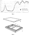
- Fig.4 illustrates a comparison between radiation efficiency of the present antenna assembly and radiation efficiency of a traditional antenna assembly under the same condition (i.e. the same distance between the antenna and the metal housing), by taking WI-FI (WIreless-Fidelity) at dual-frequency of 2.4 GHz/5 GHz as an example.
- the X-axis in Fig. 4 represents the radiation frequency and the Y-axis in Fig. 4 represents the radiation efficiency.
- the traditional antenna assembly has an antenna radiation efficiency of 7.5% at 2.4GHz.
- the antenna assembly according to the embodiments of the disclosure since the metal housing forms a part of the antenna and thus is involved in radiation of the antenna due to generation of resonance, the radiation efficiency of the antenna is improved.
- the antenna radiation efficiency at 2.4GHz reaches around 20%.
- the electronic device 500 includes the antenna assembly shown in any one of the Fig. 1, Fig. 2 and Fig. 3 .
- the antenna assembly includes an antenna 510, a PCB 520, and a metal housing 530.
- the metal housing 520 may be a metal housing of the electronic device 500; Fig. 5 is illustrated by taking the metal housing 530 being the seamless metal back cover of the electronic device 500 as an example.
- the electronic device 500 also include other required components.
- the electronic device 500 when it is a tablet, also includes a display module 540 and a battery 550.
- the electronic device 500 may also include components such as sensors, physical buttons, etc, which will not be described redundantly.
Landscapes
- Engineering & Computer Science (AREA)
- Computer Hardware Design (AREA)
- Computer Networks & Wireless Communication (AREA)
- General Engineering & Computer Science (AREA)
- Support Of Aerials (AREA)
Abstract
The present disclosure discloses an antenna assembly and an electronic device, which belong to the field of antenna. The antenna assembly includes an antenna (120), a printed circuit board (PCB) (140) and a metal housing (160); wherein the antenna (120) and the PCB (140) are electrically connected through a feeding point (142); and the antenna (120) and the metal housing (140) are electrically connected through a ground point (162).
Description
- The present disclosure generally relates to the field of antenna technology, and more particularly to an antenna assembly and electronic device.
- With continuous development of processes for manufacturing an electronic device, more and more electronic devices are provided with a full metal back cover. Compared to a traditional plastic back cover, a full metal back cover looks more beautiful and enables better tactile experience.
- However, the full metal back cover will affect radiation efficiency of an antenna in an electronic device, especially in the case where an electronic device is developed toward thinner and weight lighter, because the smaller the antenna is positioned within and separated from the full metal back cover, the greater the radiation efficiency of the antenna is affected.
- In view of the fact that the radiation efficiency of the antenna will be affected greatly as the antenna is placed closer to the full metal back cover in the case where an electronic device is developed toward thinner and weight lighter, the present disclosure provides an antenna assembly and electronic device. The technical solutions are as follows.
- According to a first aspect of embodiments of the present disclosure, an antenna assembly is provided. The antenna assembly includes: an antenna, a PCB (Printed Circuit Board) and a metal housing; wherein the antenna and the PCB are electrically connected through a feeding point; and the antenna and the metal housing are electrically connected through a ground point.
- In an alternative embodiment, the PCB has a ground point which is electrically connected to the metal housing. The metal housing directs currents flowing through the antenna and the metal housing back to the PCB.
- In an alternative embodiment, the antenna assembly further includes an intermediary metal frame, wherein the intermediary metal frame is electrically connected with both a ground point of the PCB and the metal housing. The intermediary metal frame directs currents flowing through the antenna and the metal housing back to the PCB.
- In an alternative embodiment, the metal housing is a seamless housing structure.
- In an alternative embodiment, the antenna includes at least one of a loop antenna, an inverted F-type antenna and a planar inverted-F antenna.
- According to a second aspect of embodiments of the present disclosure, an electronic device is provided. The electronic device includes the antenna assembly according to any one embodiment according to the first aspect.
- In an alternative embodiment, the metal housing is a seamless metal back cover of the electronic device.
- By connecting the antenna with a feeding point of the PCB electrically and connecting the antenna with the metal housing through ground points electrically such that the metal housing forms a part of the antenna, the present disclosure can solves the problem that the radiation efficiency of the antenna will be affected greatly as the antenna is placed closer to the full metal back cover in the case where an electronic device is developed toward thinner and weight lighter and thus attain the effects of increased radiation efficiency of the antenna by directing currents flowing through the antenna back to the ground via the metal housing and causing resonance of the metal housing.
- It is to be understood that both the forgoing general descriptions and the following detailed descriptions are exemplary and explanatory only, and are not restrictive of the present disclosure.
- The accompanying drawings, which are incorporated in and constitute a part of this specification, illustrate embodiments consistent with the disclosure and, together with the description, serve to explain the principles of the disclosure.
-
Fig. 1 is a schematic structural view of an antenna assembly according to an exemplary embodiment of the disclosure. -
Fig. 2 is a schematic structural view of an antenna assembly according to another exemplary embodiment of the disclosure. -
Fig. 3 is a schematic structural view of an antenna assembly according to yet another exemplary embodiment of the disclosure. -
Fig. 4 is a diagram illustrating comparison between radiation efficiency of the present antenna assembly and radiation efficiency of a traditional antenna assembly. -
Fig. 5 is a schematic structural view of an electronic device according to an exemplary embodiment of the disclosure. - Reference will now be made in detail to exemplary embodiments, examples of which are illustrated in the accompanying drawings. The following description refers to the accompanying drawings in which the same numbers in different drawings represent the same or similar elements unless otherwise described. The implementations set forth in the following description of exemplary embodiments do not represent all implementations consistent with the disclosure. Instead, they are merely examples of devices and methods consistent with aspects related to the disclosure as recited in the appended claims.
- The antenna assembly according to various embodiments of the disclosure can be used in an electronic device configured with a metal housing. The electronic device may be a smart phone, a tablet, a smart TV, an e-book reader, an MP3 (Moving Picture Experts Group Audio Layer III) player or MP4 (Moving Picture Experts Group Audio Layer IV) player, etc. The metal housing may be a seamless housing structure. For example, the metal housing may be a seamless metal back cover of a tablet. For convenience of description, the following embodiments are only illustrated by taking an antenna assembly for a tablet as an example, which is not intended to limit the disclosure.
- Referring to
Fig. 1 , there is shown a schematic structural view of anantenna assembly 100 according to an exemplary embodiment of the disclosure. Theantenna assembly 100 includes: anantenna 120, aPCB 140 and ametal housing 160. - The
antenna 120 and the PCB 140 are electrically connected through afeeding point 142. - The
antenna 120 may be a loop antenna, an inverted F-type antenna, or a planar inverted-F antenna, etc. Further, theantenna 120 and the PCB 140 are connected through a feeder. The disclosure does not limit the type of the antenna. - The
feeding point 142 is located on the PCB 140. ThePCB 140 transmits currents to theantenna 120 via thefeeding point 142 so that theantenna 120 generates electromagnetic radiation based on the currents. - The
antenna 120 and themetal housing 160 are electrically connected through aground point 162. - The
metal housing 160 may be a seamless housing structure such that currents can be conducted between any two points on themetal housing 160. For example, the metal housing may be a seamless metal back cover of the tablet. - The
ground point 162 is located on themetal housing 160. Themetal housing 160 is electrically connected with theantenna 120 via theground point 162, so that currents flowing through theantenna 120 go through themetal housing 160. As such, themetal housing 160 forms a part of theantenna 120, and will generates resonance under the effect of the currents, and thereby radiation efficiency of theantenna assembly 100 can be improved. - It should be noted that, the
antenna 120 includes anantenna feeding point 122 and anantenna ground point 124, and theantenna 120 is electrically connected with thefeeding point 142 of the PCB 140 via theantenna feeding point 122, and is electrically connected with theground point 162 of the metal housing 160via theantenna ground point 124. - In summary, in the antenna assembly according to the present embodiment, the antenna is electrically connected with a feeding point of the PCB and also is electrically connected with the metal housing through ground points such that the metal housing forms a part of the antenna, it is able to solve a problem that the radiation efficiency of the antenna will be affected greatly as the antenna is placed closer to the full metal back cover in the case where an electronic device is developed toward thinner and weight lighter and thus attain the effects of increased radiation efficiency of the antenna by directing currents flowing through the antenna back to the ground via the metal housing and causing resonance of the metal housing. Referring to
Fig. 2 , it shows a schematic structural view of anantenna assembly 200 according to another exemplary embodiment of the disclosure. Theantenna assembly 200 includes: anantenna 220, aPCB 240 and ametal housing 260. - The
antenna 220 and thePCB 240 are electrically connected through afeeding point 242. - As shown in
Fig. 2 , theantenna 220 is electrically connected with thefeeding point 242 of the PCB 240 via anantenna feeding point 222. - The
antenna 220 and themetal housing 260 are electrically connected through aground point 262. - As shown in
Fig. 2 , theantenna 220 is electrically connected with theground point 262 of themetal housing 260 via anantenna ground point 224. - The
ground point 244 of the PCB 240 is electrically connected to themetal housing 260. - Unlike the antenna assembly shown in
Fig. 1 , thePCB 240 is also provided with aground point 244, through which thePCB 240 is electrically connected with themetal housing 260. Themetal housing 260 directs currents flowing through theantenna 220 and themetal housing 260 back to the PCB 240. - With the above described connections, when the
antenna assembly 200 works, thePCB 240 transmits currents to theantenna feeding point 222 of theantenna 220 via thefeeding point 242, and with flowing of the currents through theantenna 220, electromagnetic radiation is generated. Since theantenna ground point 224 of theantenna 220 and theground point 262 of themetal housing 260 are electrically connected, the currents flowing through theantenna 220 then flows to themetal housing 260, and then flows back to thePCB 240 through theground point 244 connecting themetal housing 260 andPCB 240. A transmission path for the currents is shown inFig. 2 as a dotted line. - In a traditional antenna assembly, an antenna ground point of the antenna and a ground point of the PCB are directly connected such that the currents flowing through the antenna directly flows back to the PCB without flowing through the metal housing, and thus the metal housing is not involved in radiation of the antenna assembly. Therefore, the radiation efficiency of the antenna is only related to distance between the antenna and the metal housing, and the smaller the distance is, the lower the radiation efficiency of the antenna is.
- In the antenna assembly according to the present embodiment, however, the
metal housing 260 forms a part of theantenna 220 such that radiation area of theantenna 220 is greatly increased, and under the effect of the currents, themetal housing 260 generates resonance, and thereby the radiation efficiency of theantenna assembly 200 is improved significantly. - In summary, in the antenna assembly according to the present embodiment, the antenna is electrically connected with a feeding point of the PCB and also is electrically connected with the metal housing through ground points such that the metal housing forms a part of the antenna, it is able to solve an problem that the radiation efficiency of the antenna will be affected greatly as the antenna is placed smaller to the full metal back cover in the case where an electronic device is developed toward thinner and weight lighter and thus attain the effects of increased radiation efficiency of the antenna by directing currents flowing through the antenna back to the ground via the metal housing and causing resonance of the metal housing.
- Referring to
Fig. 3 , there is shown a schematic structural view of anantenna assembly 300 according to yet another exemplary embodiment of the disclosure. Theantenna assembly 300 includes: anantenna 320, aPCB 340 and ametal housing 360. - The
antenna 320 and thePCB 340 are electrically connected through afeeding point 342. - As shown in
Fig. 3 , theantenna 320 is electrically connected with thefeeding point 342 of thePCB 340 via anantenna feeding point 322. - The
antenna 320 and themetal housing 360 are electrically connected through aground point 362. - As shown in
Fig. 3 , theantenna 320 is electrically connected with theground point 362 of themetal housing 360 via anantenna ground point 324. - In order to improve stability of the
antenna assembly 300 in an electronic device, thePCB 340 is fixed on anintermediary metal frame 380 and electrically connected with theintermediary metal frame 380 through aground point 344, as shown inFig. 3 . - The
intermediary metal frame 380 is fixed on themetal housing 360 and is electrically connected with themetal housing 360. Theintermediary metal frame 380 may be made of an aluminum alloy material. - It should be noted that, the present embodiment is only illustrated by taking a PCB fixed on an intermediary metal frame as an example. In practice, a battery and other components of the electronic device may also be fixed on the intermediary metal frame in order to improve stability of the various components of the electronic device, which is not limited in the disclosure.
- The
PCB 340 transmits currents to theantenna feeding point 322 of theantenna 320 via thefeeding point 342, and with flowing of currents through theantenna 320, electromagnetic radiation is generated. Since theantenna ground point 324 of theantenna 320 and theground point 362 of themetal housing 360 are electrically connected, the currents, after flowing through theantenna 320 then flows to themetal housing 360. The currents flow through themetal housing 360, and then flows to theintermediary metal frame 380 which is electrically connected to themetal housing 360, and then flows back to thePCB 340 via theground point 344. - Similarly with the operation principle of the antenna assembly shown in
Fig. 2 , themetal housing 360 forms a part of theantenna 320 such that radiating area of theantenna 320 is greatly increased, and under the effect of the currents, themetal housing 360 generates resonance, and thereby the radiation efficiency of theantenna assembly 300 is improved significantly. - In summary, in the antenna assembly according to the present embodiment, the antenna is electrically connected with a feeding point of the PCB and also is electrically connected with the metal housing through ground points such that the metal housing forms a part of the antenna, it is able to solve a problem that the radiation efficiency of the antenna will be affected greatly as the antenna is placed closer to the full metal back cover in the case where an electronic device is developed toward thinner and weight lighter and thus attain the effects of increased radiation efficiency of the antenna by directing currents flowing through the antenna back to the ground via the metal housing and causing resonance of the metal housing.
- Further, in the present embodiment, by fixing the PCB on the intermediary metal frame and placing the intermediary metal frame on the metal housing, not only the antenna radiation efficiency can be improved, but also stability of the PCB and other components can be ensured.
-
Fig.4 illustrates a comparison between radiation efficiency of the present antenna assembly and radiation efficiency of a traditional antenna assembly under the same condition (i.e. the same distance between the antenna and the metal housing), by taking WI-FI (WIreless-Fidelity) at dual-frequency of 2.4 GHz/5 GHz as an example. The X-axis inFig. 4 represents the radiation frequency and the Y-axis inFig. 4 represents the radiation efficiency. - In a low frequency band, since wavelength in the low frequency band is longer, the radiation efficiency of the antenna will be very low if the distance between the antenna and the metal housing is short. For example, the traditional antenna assembly has an antenna radiation efficiency of 7.5% at 2.4GHz. With the antenna assembly according to the embodiments of the disclosure, since the metal housing forms a part of the antenna and thus is involved in radiation of the antenna due to generation of resonance, the radiation efficiency of the antenna is improved. The antenna radiation efficiency at 2.4GHz reaches around 20%. Obviously, by using the antenna assembly according to the embodiments of the disclosure, the radiation efficiency of the antenna can be significantly improved, especially in the low frequency band.
- Referring to
Fig. 5 , there is shown a schematic structural view of an electronic device 500 according to an exemplary embodiment of the present disclosure. The electronic device 500 includes the antenna assembly shown in any one of theFig. 1, Fig. 2 and Fig. 3 . The antenna assembly includes anantenna 510, aPCB 520, and ametal housing 530. - The
metal housing 520 may be a metal housing of the electronic device 500;Fig. 5 is illustrated by taking themetal housing 530 being the seamless metal back cover of the electronic device 500 as an example. - It should be noted that the electronic device 500 also include other required components. For example, as shown in
Fig. 5 , the electronic device 500, when it is a tablet, also includes adisplay module 540 and abattery 550. In other potential implementations, the electronic device 500 may also include components such as sensors, physical buttons, etc, which will not be described redundantly. - Other embodiments of the disclosure will be apparent to those skilled in the art from consideration of the specification and practice of the embodiments disclosed here. This application is intended to cover any variations, uses, or adaptations of the disclosure following the general principles thereof and including such departures from the present disclosure as come within known or customary practice in the art. The specification and embodiments are merely considered to be exemplary and the substantive scope of the disclosure is limited only by the appended claims.
- It should be understood that the disclosure is not limited to the precise structure as described above and shown in the figures, but can have various modification and alternations without departing from the scope of the disclosure. The scope of the disclosure is limited only by the appended claims.
Claims (9)
- An antenna assembly, characterized by comprising:an antenna (120), a printed circuit board (PCB) (140) and a metal housing (160);wherein the antenna (120) and the PCB (140) are electrically connected through a feeding point (142); andwherein the antenna (120) and the metal housing (160) are electrically connected through a ground point (162).
- The antenna assembly of claim 1, wherein the PCB (140) has a ground point (244) which is electrically connected to the metal housing (160).
- The antenna assembly of claim 2, wherein the metal housing (160) directs currents flowing through the antenna (120) and the metal housing (160) back to the PCB (140).
- The antenna assembly of claim 1, wherein the antenna assembly further comprises an intermediary metal frame (380), wherein the intermediary metal frame (380) is electrically connected with both a ground point (344) of the PCB (140) and the metal housing (160).
- The antenna assembly of claim 4, wherein the intermediary metal frame (380) directs currents flowing through the antenna (120) and the metal housing (160) back to the PCB (140).
- The antenna assembly of any one of claims 1 to 5, wherein the metal housing (160) is a seamless housing structure.
- The antenna assembly of any one of claims 1 to 5, wherein the antenna (120) comprises at least one of a loop antenna, an inverted F-type antenna and a planar inverted-F antenna.
- An electronic device, characterized by comprising the antenna assembly of any one of claims 1 to 7.
- The electronic device of claim 8, wherein the metal housing (160) is a seamless metal back cover of the electronic device.
Applications Claiming Priority (1)
| Application Number | Priority Date | Filing Date | Title |
|---|---|---|---|
| CN201510770242.3A CN106684555B (en) | 2015-11-11 | 2015-11-11 | Antenna module and electronic equipment |
Publications (1)
| Publication Number | Publication Date |
|---|---|
| EP3168929A1 true EP3168929A1 (en) | 2017-05-17 |
Family
ID=57281135
Family Applications (1)
| Application Number | Title | Priority Date | Filing Date |
|---|---|---|---|
| EP16198120.4A Withdrawn EP3168929A1 (en) | 2015-11-11 | 2016-11-10 | Antenna assembly and electronic device |
Country Status (4)
| Country | Link |
|---|---|
| US (1) | US20170133742A1 (en) |
| EP (1) | EP3168929A1 (en) |
| CN (1) | CN106684555B (en) |
| WO (1) | WO2017080322A1 (en) |
Families Citing this family (4)
| Publication number | Priority date | Publication date | Assignee | Title |
|---|---|---|---|---|
| US10193214B2 (en) * | 2016-07-29 | 2019-01-29 | Motorola Mobility Llc | Near field communication on a seamless metal band and metal backed device |
| WO2019084706A1 (en) * | 2017-10-30 | 2019-05-09 | 深圳传音制造有限公司 | Antenna assembly and mobile terminal |
| CN110649371B (en) * | 2019-09-27 | 2021-03-16 | 西南交通大学 | Antenna and mobile terminal equipment thereof |
| CN114079174B (en) * | 2020-08-19 | 2023-02-10 | 华为技术有限公司 | Connecting assembly and electronic equipment |
Citations (3)
| Publication number | Priority date | Publication date | Assignee | Title |
|---|---|---|---|---|
| US20100090921A1 (en) * | 2008-10-13 | 2010-04-15 | Samsung Electronics Co. Ltd. | Built-in antenna device for portable wireless terminal |
| EP2784873A1 (en) * | 2013-03-29 | 2014-10-01 | Pantech Co., Ltd. | Terminal including multiband antenna using conductive border |
| CN203932323U (en) * | 2014-05-28 | 2014-11-05 | 瑞声精密制造科技(常州)有限公司 | Be applicable to have the antenna system of the mobile terminal of metal frame structure |
Family Cites Families (7)
| Publication number | Priority date | Publication date | Assignee | Title |
|---|---|---|---|---|
| US8432678B2 (en) * | 2010-01-06 | 2013-04-30 | Apple Inc. | Component assembly |
| TWI573321B (en) * | 2013-05-09 | 2017-03-01 | 富智康(香港)有限公司 | Wireless communication device |
| US20150070239A1 (en) * | 2013-09-10 | 2015-03-12 | Mediatek Inc. | Antenna |
| KR102081392B1 (en) * | 2013-11-04 | 2020-02-25 | 삼성전자주식회사 | An electronic device including an antenna apparatus |
| CN204289695U (en) * | 2014-12-31 | 2015-04-22 | 惠州硕贝德无线科技股份有限公司 | A kind of double-ring antenna utilizing mobile phone metal back cover |
| CN105024135A (en) * | 2015-07-06 | 2015-11-04 | 昆山联滔电子有限公司 | Cellphone antenna |
| KR102306080B1 (en) * | 2015-08-13 | 2021-09-30 | 삼성전자주식회사 | Antenna and electronic device including the antenna |
-
2015
- 2015-11-11 CN CN201510770242.3A patent/CN106684555B/en active Active
-
2016
- 2016-09-26 WO PCT/CN2016/100063 patent/WO2017080322A1/en not_active Ceased
- 2016-11-04 US US15/343,238 patent/US20170133742A1/en not_active Abandoned
- 2016-11-10 EP EP16198120.4A patent/EP3168929A1/en not_active Withdrawn
Patent Citations (3)
| Publication number | Priority date | Publication date | Assignee | Title |
|---|---|---|---|---|
| US20100090921A1 (en) * | 2008-10-13 | 2010-04-15 | Samsung Electronics Co. Ltd. | Built-in antenna device for portable wireless terminal |
| EP2784873A1 (en) * | 2013-03-29 | 2014-10-01 | Pantech Co., Ltd. | Terminal including multiband antenna using conductive border |
| CN203932323U (en) * | 2014-05-28 | 2014-11-05 | 瑞声精密制造科技(常州)有限公司 | Be applicable to have the antenna system of the mobile terminal of metal frame structure |
Also Published As
| Publication number | Publication date |
|---|---|
| US20170133742A1 (en) | 2017-05-11 |
| CN106684555A (en) | 2017-05-17 |
| WO2017080322A1 (en) | 2017-05-18 |
| CN106684555B (en) | 2019-03-08 |
Similar Documents
| Publication | Publication Date | Title |
|---|---|---|
| CN106410428B (en) | Antenna device and electronic device including the same | |
| CN104795623B (en) | Mobile device and manufacturing method thereof | |
| US10276938B2 (en) | Mobile terminal device | |
| US9300055B2 (en) | Mobile device with two antennas and antenna switch modules | |
| KR101604759B1 (en) | Antenna assembly and portable terminal having the same | |
| CN105655701B (en) | Antenna device and mobile terminal | |
| KR102208207B1 (en) | Antenna for Mobile Device using Case | |
| US20160111773A1 (en) | Electronic device | |
| US20160351991A1 (en) | NFC Antenna Structure | |
| EP3168929A1 (en) | Antenna assembly and electronic device | |
| US20130044031A1 (en) | Antenna module | |
| US11165153B2 (en) | Antenna and terminal | |
| CN106229672A (en) | A kind of NFC antenna structure and mobile terminal | |
| JP2020524919A (en) | Electronic device and its antenna structure | |
| WO2019033311A1 (en) | Terminal device | |
| CN107464997B (en) | Metal shell and electronic equipment | |
| CN204011708U (en) | Wireless fidelity WIFI auxiliary antenna | |
| CN208045684U (en) | Antenna structure for electric terminal and the electric terminal with the antenna structure | |
| US20130141285A1 (en) | Electronic devie with structure for enhancing antenna performance | |
| US9386132B2 (en) | Wireless communication device | |
| CN109301476A (en) | A kind of metal back cover plate LTE ultra-wide band antenna | |
| CN206022629U (en) | Mobile terminal | |
| CN103928753A (en) | A mobile phone and its antenna | |
| CN104241809B (en) | The wireless communication device of antenna module and the application antenna module | |
| CN207800899U (en) | Antenna structure and electronic equipment |
Legal Events
| Date | Code | Title | Description |
|---|---|---|---|
| PUAI | Public reference made under article 153(3) epc to a published international application that has entered the european phase |
Free format text: ORIGINAL CODE: 0009012 |
|
| AK | Designated contracting states |
Kind code of ref document: A1 Designated state(s): AL AT BE BG CH CY CZ DE DK EE ES FI FR GB GR HR HU IE IS IT LI LT LU LV MC MK MT NL NO PL PT RO RS SE SI SK SM TR |
|
| AX | Request for extension of the european patent |
Extension state: BA ME |
|
| STAA | Information on the status of an ep patent application or granted ep patent |
Free format text: STATUS: THE APPLICATION IS DEEMED TO BE WITHDRAWN |
|
| 18D | Application deemed to be withdrawn |
Effective date: 20171118 |