EP3168928A1 - Electronic device and antenna - Google Patents
Electronic device and antenna Download PDFInfo
- Publication number
- EP3168928A1 EP3168928A1 EP16197267.4A EP16197267A EP3168928A1 EP 3168928 A1 EP3168928 A1 EP 3168928A1 EP 16197267 A EP16197267 A EP 16197267A EP 3168928 A1 EP3168928 A1 EP 3168928A1
- Authority
- EP
- European Patent Office
- Prior art keywords
- antenna
- electronic device
- field non
- communication
- contact communication
- Prior art date
- Legal status (The legal status is an assumption and is not a legal conclusion. Google has not performed a legal analysis and makes no representation as to the accuracy of the status listed.)
- Granted
Links
Images











Classifications
-
- H—ELECTRICITY
- H01—ELECTRIC ELEMENTS
- H01Q—ANTENNAS, i.e. RADIO AERIALS
- H01Q7/00—Loop antennas with a substantially uniform current distribution around the loop and having a directional radiation pattern in a plane perpendicular to the plane of the loop
- H01Q7/06—Loop antennas with a substantially uniform current distribution around the loop and having a directional radiation pattern in a plane perpendicular to the plane of the loop with core of ferromagnetic material
-
- H—ELECTRICITY
- H01—ELECTRIC ELEMENTS
- H01Q—ANTENNAS, i.e. RADIO AERIALS
- H01Q7/00—Loop antennas with a substantially uniform current distribution around the loop and having a directional radiation pattern in a plane perpendicular to the plane of the loop
-
- H—ELECTRICITY
- H01—ELECTRIC ELEMENTS
- H01Q—ANTENNAS, i.e. RADIO AERIALS
- H01Q1/00—Details of, or arrangements associated with, antennas
- H01Q1/12—Supports; Mounting means
- H01Q1/22—Supports; Mounting means by structural association with other equipment or articles
- H01Q1/2208—Supports; Mounting means by structural association with other equipment or articles associated with components used in interrogation type services, i.e. in systems for information exchange between an interrogator/reader and a tag/transponder, e.g. in Radio Frequency Identification [RFID] systems
- H01Q1/2216—Supports; Mounting means by structural association with other equipment or articles associated with components used in interrogation type services, i.e. in systems for information exchange between an interrogator/reader and a tag/transponder, e.g. in Radio Frequency Identification [RFID] systems used in interrogator/reader equipment
-
- H—ELECTRICITY
- H01—ELECTRIC ELEMENTS
- H01Q—ANTENNAS, i.e. RADIO AERIALS
- H01Q1/00—Details of, or arrangements associated with, antennas
- H01Q1/12—Supports; Mounting means
- H01Q1/22—Supports; Mounting means by structural association with other equipment or articles
- H01Q1/2291—Supports; Mounting means by structural association with other equipment or articles used in Bluetooth® or Wi-Fi® devices of Wireless Local Area Networks [WLAN]
-
- H—ELECTRICITY
- H01—ELECTRIC ELEMENTS
- H01Q—ANTENNAS, i.e. RADIO AERIALS
- H01Q1/00—Details of, or arrangements associated with, antennas
- H01Q1/12—Supports; Mounting means
- H01Q1/22—Supports; Mounting means by structural association with other equipment or articles
- H01Q1/24—Supports; Mounting means by structural association with other equipment or articles with receiving set
- H01Q1/241—Supports; Mounting means by structural association with other equipment or articles with receiving set used in mobile communications, e.g. GSM
- H01Q1/242—Supports; Mounting means by structural association with other equipment or articles with receiving set used in mobile communications, e.g. GSM specially adapted for hand-held use
- H01Q1/243—Supports; Mounting means by structural association with other equipment or articles with receiving set used in mobile communications, e.g. GSM specially adapted for hand-held use with built-in antennas
-
- H—ELECTRICITY
- H01—ELECTRIC ELEMENTS
- H01Q—ANTENNAS, i.e. RADIO AERIALS
- H01Q1/00—Details of, or arrangements associated with, antennas
- H01Q1/12—Supports; Mounting means
- H01Q1/22—Supports; Mounting means by structural association with other equipment or articles
- H01Q1/24—Supports; Mounting means by structural association with other equipment or articles with receiving set
- H01Q1/248—Supports; Mounting means by structural association with other equipment or articles with receiving set provided with an AC/DC converting device, e.g. rectennas
-
- H—ELECTRICITY
- H01—ELECTRIC ELEMENTS
- H01Q—ANTENNAS, i.e. RADIO AERIALS
- H01Q1/00—Details of, or arrangements associated with, antennas
- H01Q1/36—Structural form of radiating elements, e.g. cone, spiral, umbrella; Particular materials used therewith
- H01Q1/38—Structural form of radiating elements, e.g. cone, spiral, umbrella; Particular materials used therewith formed by a conductive layer on an insulating support
-
- H—ELECTRICITY
- H01—ELECTRIC ELEMENTS
- H01Q—ANTENNAS, i.e. RADIO AERIALS
- H01Q1/00—Details of, or arrangements associated with, antennas
- H01Q1/50—Structural association of antennas with earthing switches, lead-in devices or lightning protectors
-
- H—ELECTRICITY
- H01—ELECTRIC ELEMENTS
- H01Q—ANTENNAS, i.e. RADIO AERIALS
- H01Q21/00—Antenna arrays or systems
- H01Q21/28—Combinations of substantially independent non-interacting antenna units or systems
-
- H—ELECTRICITY
- H01—ELECTRIC ELEMENTS
- H01Q—ANTENNAS, i.e. RADIO AERIALS
- H01Q5/00—Arrangements for simultaneous operation of antennas on two or more different wavebands, e.g. dual-band or multi-band arrangements
- H01Q5/20—Arrangements for simultaneous operation of antennas on two or more different wavebands, e.g. dual-band or multi-band arrangements characterised by the operating wavebands
-
- H—ELECTRICITY
- H01—ELECTRIC ELEMENTS
- H01Q—ANTENNAS, i.e. RADIO AERIALS
- H01Q5/00—Arrangements for simultaneous operation of antennas on two or more different wavebands, e.g. dual-band or multi-band arrangements
- H01Q5/30—Arrangements for providing operation on different wavebands
- H01Q5/307—Individual or coupled radiating elements, each element being fed in an unspecified way
- H01Q5/314—Individual or coupled radiating elements, each element being fed in an unspecified way using frequency dependent circuits or components, e.g. trap circuits or capacitors
-
- H—ELECTRICITY
- H01—ELECTRIC ELEMENTS
- H01Q—ANTENNAS, i.e. RADIO AERIALS
- H01Q5/00—Arrangements for simultaneous operation of antennas on two or more different wavebands, e.g. dual-band or multi-band arrangements
- H01Q5/30—Arrangements for providing operation on different wavebands
- H01Q5/307—Individual or coupled radiating elements, each element being fed in an unspecified way
- H01Q5/342—Individual or coupled radiating elements, each element being fed in an unspecified way for different propagation modes
- H01Q5/35—Individual or coupled radiating elements, each element being fed in an unspecified way for different propagation modes using two or more simultaneously fed points
-
- H—ELECTRICITY
- H01—ELECTRIC ELEMENTS
- H01Q—ANTENNAS, i.e. RADIO AERIALS
- H01Q9/00—Electrically-short antennas having dimensions not more than twice the operating wavelength and consisting of conductive active radiating elements
- H01Q9/04—Resonant antennas
- H01Q9/0407—Substantially flat resonant element parallel to ground plane, e.g. patch antenna
- H01Q9/0421—Substantially flat resonant element parallel to ground plane, e.g. patch antenna with a shorting wall or a shorting pin at one end of the element
-
- H—ELECTRICITY
- H04—ELECTRIC COMMUNICATION TECHNIQUE
- H04B—TRANSMISSION
- H04B5/00—Near-field transmission systems, e.g. inductive or capacitive transmission systems
- H04B5/20—Near-field transmission systems, e.g. inductive or capacitive transmission systems characterised by the transmission technique; characterised by the transmission medium
- H04B5/24—Inductive coupling
- H04B5/26—Inductive coupling using coils
-
- H—ELECTRICITY
- H04—ELECTRIC COMMUNICATION TECHNIQUE
- H04B—TRANSMISSION
- H04B5/00—Near-field transmission systems, e.g. inductive or capacitive transmission systems
- H04B5/70—Near-field transmission systems, e.g. inductive or capacitive transmission systems specially adapted for specific purposes
- H04B5/79—Near-field transmission systems, e.g. inductive or capacitive transmission systems specially adapted for specific purposes for data transfer in combination with power transfer
-
- H—ELECTRICITY
- H04—ELECTRIC COMMUNICATION TECHNIQUE
- H04B—TRANSMISSION
- H04B5/00—Near-field transmission systems, e.g. inductive or capacitive transmission systems
- H04B5/40—Near-field transmission systems, e.g. inductive or capacitive transmission systems characterised by components specially adapted for near-field transmission
- H04B5/45—Transponders
Definitions
- the present disclosure relates to an electronic device and an antenna.
- a case that covers an electronic device like a smartphone uses plastic or glass in many cases, but products using metal have been increasing in recent years.
- a requester can be provided with an image of a high quality by the metal being used in the case that covers the electronic device.
- non-contact communication by electromagnetic induction using the antenna coil (hereinafter, also referred to as non-contact communication simply) is affected particularly.
- eddy current generated on a surface of the metal affects the non-contact communication if the surface of the case formed of metal is put on a reader/writer.
- a user puts a surface that is not formed of the metal, for example, a display surface, on the reader/writer, in order to perform the non-contact communication.
- a mark representing the position that is put on the reader/writer is to be provided for the purpose of user friendly or by a request from a communication business operator.
- the mark is unable to be attached to the display region of the display, and thus the mark is to be attached to the periphery portion of the display surface, and the electronic device is to be configured so that the antenna coil is positioned under the mark.
- the antenna coil interferes an antenna for performing wireless communication with a base station or the like (for example, a cellular antenna for performing wireless communication by a cellular method), which is provided at the periphery portion of the display surface in the same way.
- the present disclosure proposes a new and improved electronic device and an antenna, which allow the wireless communication antenna and the antenna coil to coexist effectively.
- an electronic device including: a first antenna for wireless communication; a second antenna for near-field communication that forms a loop by being used together with the first antenna, at least a part of the second antenna being positioned at a back surface of a display region of a display; and a first filter that is provided in the first antenna or the second antenna, passes a signal of a frequency band used in the near-field communication to the first antenna, and blocks inflow of the signal of the frequency band used in the wireless communication into the second antenna.
- an antenna including: a first antenna for wireless communication; and a second antenna for near-field communication that forms a loop by being used together with the first antenna, at least a part of the second antenna being positioned at a back surface of a display region of a display.
- the new and improved electronic device and the antenna which allow the wireless communication antenna and the antenna coil to coexist effectively, can be provided.
- the metal being used in the case that covers the electronic device has an influence on non-contact communication by electromagnetic induction that uses the antenna coil particularly.
- the electronic device is equipped with the antenna coil for performing the non-contact communication
- eddy current generated on a surface of the metal has an influence on the non-contact communication if a surface of the case formed of metal is put on a reader/writer.
- a user puts a surface that is not formed of the metal, for example, a display surface, on the reader/writer, in order to perform the non-contact communication.
- a mark representing the position that is put on the reader/writer is to be provided.
- a mark is unable to be attached to a display region of the display.
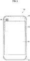
- FIG. 1 is an explanatory diagram illustrating an exemplary configuration of an electronic device 10.
- the electronic device 10 illustrated in FIG. 1 is to describe the overview of the embodiment of the present disclosure.
- the electronic device 10 illustrated in FIG. 1 is a smartphone, for example, and includes a main antenna 11 for wireless communication (hereinafter, also referred to as "cellular communication") by a cellular method which is provided at a lower portion of the electronic device 10, a cellular communication sub-antenna 12 which is provided at an upper portion of the electronic device 10, and an antenna coil 13 that is provided under a display region 15 of a display.
- cellular communication wireless communication
- the main antenna 11, the sub-antenna 12, and the antenna coil 13 are provided in an inner portion of the electronic device 10, but in FIG. 1 the main antenna 11 and the sub-antenna 12 are illustrated in the drawing to be provided on a front surface of the electronic device 10, for convenience of explanation. Also, a back surface of the electronic device 10 illustrated in FIG. 1 is covered with a cover made of metal such as aluminum.
- the sub-antenna 12 is not limited to usage in the cellular communication.
- the sub-antenna 12 may be used in a wireless LAN and a global navigation satellite system (GNSS), such as a global positioning network (GPS), GLONASS, and GALILEO as well.
- GNSS global navigation satellite system
- GPS global positioning network
- GLONASS global positioning network
- GALILEO global positioning network
- the display surface is directed to the reader/writer.
- the user can know which position of the electronic device 10 is to be put on the reader/writer if there is a mark representing a rough position of the antenna coil 13.
- a mark 14 for putting the electronic device 10 on the reader/writer is unable to be attached to the display region 15 of the display as in FIG. 1 .
- the electronic device 10 is configured such that the mark 14 is attached to a periphery portion of the display surface and the antenna coil 13 is positioned under the mark 14.
- FIG. 2 is an explanatory diagram illustrating an exemplary configuration of the electronic device 10.
- FIG. 2 illustrates an exemplary configuration of the electronic device 10 in which the antenna coil 13 is moved upward from the state of FIG. 1 .
- a part of the antenna coil 13 is positioned at an outside of the display region 15 of the display, so that the mark 14 can be attached to the outside of the display region 15 of the display as in FIG. 2 .
- the antenna coil 13 gets close to the sub-antenna 12 this time.
- the sub-antenna 12 and the antenna coil 13 get close to each other, the sub-antenna 12 and the antenna coil 13 impair the performance mutually.
- the present case discloser has performed an intense study with regard to a technology that allows an antenna for performing near-field non-contact communication with a reader/writer and an antenna for performing wireless communication with a base station or the like to coexist effectively, in consideration of the above point.
- the present case discloser has devised a technology that allows an antenna for performing near-field non-contact communication with a reader/writer and an antenna for performing wireless communication with a base station or the like to coexist effectively, as described below.
- FIG. 3 is an explanatory diagram illustrating the overview of the embodiment of the present disclosure.
- FIG. 3 illustrates an exemplary configuration of an electronic device 100 in which an antenna for performing near-field non-contact communication with the reader/writer and an antenna for performing wireless communication with a base station or the like coexist.
- the electronic device 100 illustrated in FIG. 3 is a smartphone, for example, and includes a cellular communication main antenna 101 that is provided at a lower portion of the electronic device 100, a cellular communication sub-antenna 102 that is provided at an upper portion of the electronic device 100, and a near-field non-contact communication antenna 103 that is provided under a display region 110 of the display.
- the main antenna 101, the sub-antenna 102, and the near-field non-contact communication antenna 103 are provided in an inner portion of the electronic device 100.
- a back surface of the electronic device 100 illustrated in FIG. 3 is covered with a cover of metal such as aluminum.
- the electronic device 100 is characterized in configuring a loop antenna with the sub-antenna 102 and the near-field non-contact communication antenna 103.
- the user of the electronic device 100 puts the display surface on the reader/writer to perform non-contact communication between the electronic device 100 and the reader/writer, the user may put the mark 104 provided on the outside of the display region 110 of the display on the reader/writer.
- the electronic device 100 expands the operation area of the near-field non-contact communication as compared with the electronic device 10 illustrated in FIG. 1 and other drawings, by configuring the loop antenna with the sub-antenna 102 and the near-field non-contact communication antenna 103.
- the sub-antenna 102 may be used in a wireless LAN, a GNSS such as GPS, GLONASS, and GALILEO, and Bluetooth (registered trademark) as well.
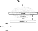
- FIG. 4 is an explanatory diagram illustrating the operation area of the near-field non-contact communication by the electronic device 10 illustrated in FIG. 1 and other drawings.
- the antenna coil 13 is provided under the display region 15 of the display as illustrated in FIG. 4 , the operation area of the near-field non-contact communication by the electronic device 10 is only in the upward direction (the direction of "Front" in FIG. 4 ) of the display surface.
- FIG. 5 is an explanatory diagram illustrating the operation area of the near-field non-contact communication by the electronic device 100 illustrated in FIG. 3 .
- the electronic device 100 can expand the operation area of the near-field non-contact communication, not only in the upward direction (the direction of "Front” in FIG. 5 ) of the display surface, but also the forward direction (the direction of "Top” in FIG. 5 ) of the electronic device 100 and the back surface direction (the direction of "Back” in FIG. 5 ) as compared with the electronic device 10 illustrated in FIG. 1 and other drawings.
- the electronic device 100 expands the operation area of the near-field non-contact communication as described above, and thus can reduce occurrence of read errors in the reader/writer.
- FIG. 6 is an explanatory diagram illustrating the exemplary configuration of the electronic device 100 according to the embodiment of the present disclosure.
- the electronic device 100 illustrated in FIG. 6 includes filters or matching components (referred to as "filter” simply in the following description) 115, 116, 117, 118, 119, 120, in addition to the above sub-antenna 102 and the near-field non-contact communication antenna 103.
- filters or matching components referred to as "filter” simply in the following description
- the sub-antenna 102 is provided in a periphery portion of the upper portion of the electronic device 100, and is produced by a laser direct structuring (LDS) antenna, a flex film, metal press processing, and the like, for example.
- LDS laser direct structuring
- the near-field non-contact communication antenna 103 is provided under the display region 110 of the display, for example, as illustrated in FIG. 3 , and is produced by an LDS film, a flex film, and the like, for example.
- the filters 115, 120 are low-pass filters, for example, and pass a signal of the near-field non-contact communication, and block a signal of the cellular communication.
- the sub-antenna 102 and the near-field non-contact communication antenna 103 are connected via the filters 115, 120, so that one turn of a loop antenna for the near-field non-contact communication is formed.
- two feeds (electricity feeding points) 113a, 113b are formed on a printed circuit board (PCB).
- the feed 113a is connected to the sub-antenna 102, and the feed 113b is connected to the near-field non-contact communication antenna 103.
- Each of the filters 116, 118, 119 is provided between the sub-antenna 102 and a ground point.
- the filter 117 is provided between the sub-antenna 102 and the feed 114.
- the filters 116, 117, 118, 119 may include matching components such as matching circuits.
- the filters 116, 118, 119 can function as an example of a communication characteristic adjustment unit of an embodiment of the present disclosure.
- the matching components such as the matching circuits alone may be provided at the positions of the filters 116, 117, 118, 119, instead of the filters.
- the filters 116, 117, 118, 119 are provided to tune the cellular communication sub-antenna 102. Thus, all of the filters 116, 117, 118, 119 block the signal of the near-field non-contact communication. Also, the filters 116, 117, 118, 119 may be used to tune a GPS antenna and a wireless LAN antenna that are not illustrated in FIG. 6 .
- the electronic device 100 has the configuration illustrated in FIG. 6 , in order to allow the antenna for performing the near-field non-contact communication with the reader/writer and the antenna for performing the wireless communication with the base station or the like to coexist effectively.
- the sub-antenna 102 and the near-field non-contact communication antenna 103 form the antenna coil, but the present disclosure is not limited to such an example, and the main antenna 101 and the near-field non-contact communication antenna 103 may form the antenna coil.
- the electronic device 100 may further include an antenna coil for near-field non-contact charging.
- FIG. 7 is an explanatory diagram illustrating another exemplary configuration of the electronic device 100 according to the embodiment of the present disclosure.
- FIG. 7 illustrates an exemplary configuration of the electronic device 100 in which an antenna coil 181 for the near-field non-contact charging is provided additionally in the electronic device 100 illustrated in FIG. 6 .
- the antenna coil 181 for the near-field non-contact charging may be provided in the electronic device 100. Note that the number of turns of the antenna coil 181 is 3 turns in FIG. 7 , but is not limited to such an example. Also, a near-field non-contact charging feed is connected to the antenna coil 181.
- FIG. 8 is an explanatory diagram illustrating another exemplary configuration of the electronic device 100 according to the embodiment of the present disclosure.
- FIG. 8 illustrates an exemplary configuration of the electronic device 100, when the near-field non-contact charging antenna 182 is shared with the main antenna 101 to form a loop antenna for the near-field non-contact charging.
- FIG. 8 includes filters 125, 126, 127, 128, 129, 130, in addition to the configuration illustrated in FIG. 6 .
- the filters 125, 130 are the low-pass filters, for example, and pass a signal of the near-field non-contact charging, and block a signal of the cellular communication.
- the main antenna 101 and the near-field non-contact charging antenna 182 are connected via the filters 125, 130, so as to form one turn of the loop antenna for the near-field non-contact charging.
- FIG. 8 illustrates a state in which two feeds 123a, 123b are formed on the PCB.
- the feed 123a is connected to the main antenna 101, and the feed 123b is connected to the near-field non-contact charging antenna 182.
- Each of the filters 126, 128, 129 is provided between the main antenna 101 and the ground point.
- the filter 127 is provided between the main antenna 101 and a feed 124.
- the filters 126, 127, 128, 129 may include matching components, such as matching circuits. Also, the matching components such as the matching circuits alone may be provided at the positions of the filters 126, 127, 128, 129, instead of the filters.
- the filters 126, 127, 128, 129 are provided to tune the cellular communication main antenna 101. Thus, all of the filters 126, 127, 128, 129 block the signal of the near-field non-contact charging.
- the near-field non-contact communication antenna 103 itself does not have a loop of one turn or more, but the present disclosure is not limited to such an example.
- the non-contact communication antenna for performing the near-field non-contact communication integrally with the sub-antenna 102 can take various forms to adjust the performance of the near-field non-contact communication.
- FIG. 9 is an explanatory diagram illustrating another exemplary configuration of the electronic device 100 according to the embodiment of the present disclosure.
- FIG. 9 illustrates an exemplary configuration of the electronic device 100 that includes a near-field non-contact communication antenna 103' having one turn in itself, instead of the near-field non-contact communication antenna 103 illustrated in FIG. 6 .
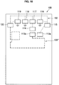
- FIG. 10 is an explanatory diagram illustrating another exemplary configuration of the electronic device 100 according to the embodiment of the present disclosure.
- FIG. 10 illustrates an exemplary configuration of the electronic device 100 that includes a near-field non-contact communication antenna 103" having one turn locally in itself, instead of the near-field non-contact communication antenna 103 illustrated in FIG. 6 .
- the near-field non-contact communication antenna for performing the near-field non-contact communication integrally with the sub-antenna 102 can take various forms. As a matter of course, it is needless to say that the form of the non-contact communication antenna for performing the near-field non-contact communication integrally with sub-antenna 102 is not limited to the ones illustrated in the above drawings.
- the near-field non-contact communication antenna 103 illustrated in FIG. 6 may also be used at the time of the near-field non-contact charging.
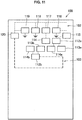
- FIG. 11 is an explanatory diagram illustrating another exemplary configuration of the electronic device 100 according to the embodiment of the present disclosure.
- FIG. 11 illustrates an exemplary configuration of the electronic device 100, when the near-field non-contact communication antenna 103 is also used in the near-field non-contact charging.
- the electronic device 100 illustrated in FIG. 11 is configured in such a manner that duplexers 112a, 112b for sharing the near-field non-contact communication antenna 103 for the near-field non-contact communication and the near-field non-contact charging and near-field non-contact charging feeds 114a, 114b are added to the electronic device 100 illustrated in FIG. 6 .
- FIG. 12A is an explanatory diagram that schematically illustrates a situation in which the duplexers 112a, 112b are connected to two feeds 113, 114. Note that, FIGS.
- 11 , 12A illustrate the situation in which the duplexers 112a, 112b are connected to the two feeds 113, 114, but what is connected to the two feeds 113, 114 may be a duplexer, a filter, or a switch.
- the duplexers 112a, 112b are provided to share the near-field non-contact communication antenna 103 for the near-field non-contact communication and the near-field non-contact charging.
- the duplexers 112a, 112b can prevent the signal of the near-field non-contact communication from flowing into the system of the near-field non-contact charging, and the signal of the near-field non-contact charging from flowing into the near-field non-contact communication, respectively.
- the electronic device 100 can share the near-field non-contact communication antenna 103 for the near-field non-contact communication and the near-field non-contact charging, by providing the duplexers 112a, 112b as illustrated in FIGS. 11 , 12A .
- FIG. 12B is an explanatory diagram illustrating a situation in which the duplexers 112a, 112b are connected to the two feeds 113, 114 and an FM unit 171.
- the FM unit 171 has a function for modulating frequency of a music piece saved in the electronic device 100 to output the music piece toward the receiver (not illustrated in the drawings), and for receiving radio waves that are FM broadcasted from a base station of radio broadcast.
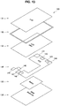
- FIG. 13 is an explanatory diagram illustrating an example of the exploded perspective view of the electronic device 100 according to the above embodiment, and is an exploded perspective view of a commonly used smartphone.
- the electronic device 100 includes a liquid crystal display (LCD) 131, a frame 132 that is formed of plastic, for example, a back surface plate 133 of the liquid crystal display, a PCB 134, a battery 135, and a backcover 136 made of metal such as aluminum.
- the metal backcover 136 can be formed with any thickness and in any shape, and can have a thickness equal to or smaller than 0.5 mm, for example.
- the PCB 134 is provided with a rear camera 141 for capturing an image of a back surface direction of the electronic device 100 (a direction in which the metal backcover 136 is provided), an ear speaker 142 for listening to a voice of a partner at the time of telephone call, a front camera 143 for capturing an image of a front surface direction of the electronic device 100 (a direction in which the LCD 131 is provided), an audio jack 144 for inserting a plug of a headphone or the like, a vibrator 145, a speaker 146, an outside input terminal 147 such as a USB, and a microphone 148.
- the positions of these devices are not limited to what are described in FIG. 13 .
- the above near-field non-contact communication antenna 103 can be provided between the LCD 131 and the back surface plate 133, for example. Note that the back surface plate 133 is not provided in the electronic device 100 in some cases, and thus the above near-field non-contact communication antenna 103 can be provided between the LCD 131 and the PCB 134, when the back surface plate 133 is not provided.
- At least a part of the above main antenna 101 and the sub-antenna 102 may be provided along an inner surface of the frame 132.
- FIG. 14A is an explanatory diagram illustrated in a perspective view of the electronic device 100 according to the above embodiment, as seen from the front surface side.
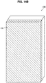
- FIG. 14B is an explanatory diagram illustrated in a perspective view of the electronic device 100 according to the above embodiment, as seen from the back surface side.
- FIG. 14A illustrates the sub-antenna 102, the near-field non-contact communication antenna 103, the feeds 113a, 113b, 114, and the filters 115, 117, 118, 120, among the exemplary configuration of the electronic device 100 illustrated in FIG. 6 .
- FIG. 14B illustrates the metal backcover 136 illustrated in FIG. 13 .
- the exterior appearance of the electronic device 100 is not limited to what is illustrated in FIGS. 14A and 14B .
- the side surface of the electronic device 100 may be covered with a metal cover.
- the side surface of the electronic device 100 alone may be covered with the metal cover.
- the back surface of the electronic device 100 may be covered with material such as plastic and glass.
- FIG. 15 is an explanatory diagram illustrated in a perspective view of another exemplary configuration of the electronic device 100 according to the above embodiment, as seen from the front surface side.
- FIG. 15 illustrates the sub-antenna 102, the near-field non-contact communication antenna 103, the feeds 113a, 113b, 114, and the filters 115, 116, 117, 118, 119, 120, among the exemplary configuration of the electronic device 100 illustrated in FIG. 6 .
- FIG. 16 is an explanatory diagram illustrated in the perspective view of another exemplary configuration of the electronic device 100 according to the above embodiment, as seen from the front surface side.
- FIG. 16 illustrates the sub-antenna 102, the near-field non-contact communication antenna 103, the feeds 113a, 113b, 114, and the filters 115, 116, 117, 118, 119, 120, among the exemplary configuration of the electronic device 100 illustrated in FIG. 6 .
- a part of the near-field non-contact communication antenna 103 illustrated in FIG. 16 is formed on the side surface of the electronic device 100, for example, an inner side of the frame 132 illustrated in FIG. 13 .
- the whole of the near-field non-contact communication antenna 103 is needless to be formed on the back surface of the LCD 131 as described above, but a part may be formed to protrude from the LCD 131.
- FIG. 17 is an explanatory diagram illustrating a more detailed exemplary configuration of the electronic device 100 according to the above embodiment.
- FIG. 17 illustrates a situation in which branches 151a, 151b are provided in the sub-antenna 102.
- the branches 151a, 151b added to the sub-antenna 102 are added to facilitate the adjustment of the resonance frequency at the time of the near-field non-contact communication, and the branches 151a, 151b are not to be provided necessarily.
- FIG. 17 illustrates a situation in which a wireless LAN antenna 152 and a GPS antenna 153 are provided in the electronic device 100. Note that the sub-antenna 102 illustrated in FIG. 17 can operate as a cellular communication main antenna.
- FIG. 18 is an explanatory diagram that illustrates a graph of reflection coefficient of the sub-antenna 102 of the electronic device 100.
- the horizontal axis of the graph illustrated in FIG. 18 represents frequency (MHz), and illustrates a range of about 700 MHz to 2700 MHz in the graph of FIG. 18 .
- the vertical axis of the graph illustrated in FIG. 18 represents reflection coefficient within a range of 0 dB to -20 dB. In the graph illustrated in FIG. 18 , the reflection coefficient drops near 880 MHz and near 1960 MHz.
- FIG. 19 is an explanatory diagram that illustrates a graph of the antenna efficiency of the sub-antenna 102.
- the horizontal axis of the graph illustrated in FIG. 19 represents frequency (MHz), and illustrates a range of about 700 MHz to 2700 MHz in the graph of FIG. 19 .
- the vertical axis of the graph illustrated in FIG. 19 represents the antenna efficiency within a range of 0 dB to -20 dB.
- the solid line of the graph of FIG. 19 illustrates an example of an ideal radiation efficiency without the mismatch loss
- the dashed line illustrates an example of an actual radiation efficiency when the sub-antenna 102 and the near-field non-contact communication antenna 103 are combined.
- the reflection coefficient drops near 880 MHz and near 1960 MHz, and thus in the graph of the antenna efficiency illustrated in FIG. 19 , the solid line and the dashed line get close to each other near 880 MHz and near 1960 MHz.
- the electronic device 100 can achieve both of the near-field non-contact communication and the cellular communication, by combining the near-field non-contact communication antenna 103 with the sub-antenna 102.
- FIGS. 20 to 27 are explanatory diagrams that illustrate graphs of examples of the characteristics of the near-field non-contact communication of the electronic device 100 according to the above embodiment.
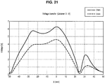
- FIGS. 20 , 21 , 22 are explanatory diagrams illustrating examples of the voltage supply characteristics of the electronic device 100 in X axis direction, in relation to the reader/writers of Listener-1, Listener-3, and Listener-6, respectively.
- each graph illustrated in FIGS. 20 , 21 , 22 represents the distance in millimeters in the X axis direction between the reader/writer and the center of the loop antenna formed by the sub-antenna 102 and the near-field non-contact communication antenna 103, with respect to the origin at the center of the loop antenna formed by the sub-antenna 102 and the near-field non-contact communication antenna 103.
- the vertical axis of each graph illustrated in FIGS. 20 , 21 , 22 represents the value of the voltage, in V, that is supplied from the electronic device 100 to the reader/writers of Listener-1, Listener-3, and Listener-6 respectively.
- the position of the center of the loop antenna formed by the sub-antenna 102 and the near-field non-contact communication antenna 103 can be the position that is moved in the direction of a side provided with the sub-antenna 102 by a predetermined distance from the center of the electronic device 100, for example.
- the solid lines of the graphs illustrated in FIGS. 20 , 21 , 22 are the voltage supply characteristics when the distance in the Z axis direction between the electronic device 100 and the reader/writer is 0 mm, and the dashed lines are the voltage supply characteristics when the distance in the Z axis direction between the electronic device 100 and the reader/writer is 5 mm.
- the voltage supply characteristic by the loop antenna formed by the sub-antenna 102 and the near-field non-contact communication antenna 103 is high near 0 mm.
- the voltage supply characteristic by the loop antenna formed by the sub-antenna 102 and the near-field non-contact communication antenna 103 satisfies a request with regard to the X axis direction, in the near-field non-contact communication.
- FIG. 23 , 24 , 25 are explanatory diagrams illustrating examples of the voltage supply characteristics of the electronic device 100 in the Y axis direction, in relation to the reader/writers of Listener-1, Listener-3, and Listener-6, respectively.
- each graph illustrated in FIG. 23 , 24 , 25 represents the distance in millimeters in the Y axis direction, between the reader/writer and the center of the loop antenna formed by the sub-antenna 102 and the near-field non-contact communication antenna 103, with respect to the origin at the center of the loop antenna formed by the sub-antenna 102 and the near-field non-contact communication antenna 103.
- the vertical axis of each graph illustrated in FIG. 23 , 24 , 25 represents the value of the voltage, in V, that is supplied from the electronic device 100 to Listener-1, Listener-3, and Listener-6 respectively.
- the solid lines of the graphs illustrated in FIG. 23 , 24 , 25 are the voltage supply characteristics when the distance in the Z axis direction between the electronic device 100 and the reader/writer is 0 mm, and the dashed lines are the voltage supply characteristics when the distance in the Z axis direction between the electronic device 100 and the reader/writer is 5 mm.
- the voltage supply characteristic by the loop antenna formed by the sub-antenna 102 and the near-field non-contact communication antenna 103 is high near 0 mm.
- the voltage supply characteristic by the loop antenna formed by the sub-antenna 102 and the near-field non-contact communication antenna 103 satisfies the request with regard to the Y axis direction in the near-field non-contact communication.
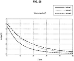
- FIG. 26 is an explanatory diagram illustrating an example of the voltage supply characteristics of the electronic device 100 in the Z axis direction, in the case of Listener-1, Listener-3, and Listener-6.
- the horizontal axis of the graph illustrated in FIG. 26 represents the distance in millimeters in the Z axis direction between the reader/writer and the center of the loop antenna formed by the sub-antenna 102 and the near-field non-contact communication antenna 103, with respect to the origin at the center of the loop antenna formed by the sub-antenna 102 and the near-field non-contact communication antenna 103. Also, the vertical axis of the graph illustrated in FIG. 26 represents the value of the voltage, in V, that is supplied from the electronic device 100 to Listener-1.
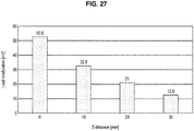
- FIG. 27 is an explanatory diagram that illustrates a bar graph of an example of the characteristics of the loop antenna formed by the sub-antenna 102 and the near-field non-contact communication antenna 103, of the electronic device 100.
- the horizontal axis represents the communication distance in millimeters in the Z axis direction between the center of the horizontal axis of the reader/writer and the center of the loop antenna formed by the sub-antenna 102 and the near-field non-contact communication antenna 103, and the vertical axis represents the load modulation level in mV.
- the voltage supply characteristic by the loop antenna formed by the sub-antenna 102 and the near-field non-contact communication antenna 103 is high near 0 mm.
- the voltage supply characteristic by the loop antenna formed by the sub-antenna 102 and the near-field non-contact communication antenna 103 also satisfies the request with regard to the Z axis direction in the near-field non-contact communication.
- the electronic device 100 is capable of the near-field non-contact communication that satisfies the request, even if the loop antenna is configured with the sub-antenna 102 and the near-field non-contact communication antenna 103.
- the electronic device 100 includes the metal backcover 136 on the back surface, but a slit can be formed in the metal backcover 136 in order to improve the characteristics of the near-field non-contact communication when the back surface side of the electronic device 100 is brought close to the reader/writer.
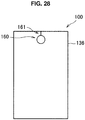
- FIGS. 28 and 29 are explanatory diagrams illustrating exemplary configurations of the backcover 136 of the electronic device 100 according to the above embodiment.
- FIGS. 28 and 29 illustrate examples of the backcover 136 in which a slit is formed.
- FIG. 28 illustrates a case in which a slit 161 is provided between a camera hole 160 that is provided at the upper portion of the center of the backcover 136 and the upper end of the backcover 136, that is, the side corresponding to the position at which the sub-antenna 102 is provided.
- FIG. 29 illustrates a case in which the slit 161 is provided between the camera hole 160 that is provided at the upper portion of the left end of the backcover 136 and the upper end of the backcover 136, that is, the side corresponding to the position at which the sub-antenna 102 is provided.
- the characteristics of the near-field non-contact communication when the back surface side is brought close to the reader/writer can be improved, by forming the slit 161 in the side corresponding to the position at which the sub-antenna 102 is provided in the metal backcover 136 as described above, which is described below.
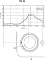
- FIG. 30 is an explanatory diagram illustrating an example of the magnetic field strength around the camera hole 160, when the camera hole 160 is provided at the upper portion of the left end of the backcover 136 as in FIG. 29 , but the slit 161 is not provided.
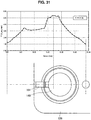
- FIG. 31 is an explanatory diagram illustrating an example of the magnetic field strength around the camera hole 160, when the camera hole 160 is provided at the upper portion of the left end of the backcover 136 as in FIG. 29 , and the slit 161 is provided as well.
- FIGS. 30 and 31 illustrate graphs at the upper sides and structures of the backcover 136 at the lower sides. Also, the horizontal axes in the graph of the upper side of FIGS. 30 and 31 correspond to the positions of the backcover 136 illustrated in the lower sides of the respective drawings, and the vertical axis represents the intensity of the magnetic field in A/m.
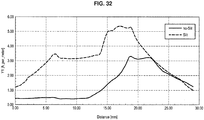
- FIG. 32 is an explanatory diagram illustrating superimposed graph parts illustrated in FIGS. 30 and 31 . It is known that the overall magnetic field is generated intensely when the slit 161 is provided, as compared with a case in which the slit 161 is not provided, as illustrated in FIG. 32 . The magnetic field being generated intensely can improve the communication characteristics at the time of the near-field non-contact communication from the electronic device 100 to the reader/writer.
- the slit 161 formed in the metal backcover 136 as illustrated in FIGS. 28 and 29 brings the effect of improving the communication characteristics when the back surface side of the electronic device 100 is brought close to the reader/writer to perform the near-field non-contact communication.
- the electronic device 100 that includes the sub-antenna 102 for performing the cellular communication and the near-field non-contact communication antenna 103 that configures the loop antenna integrally with the sub-antenna 102 is provided. Then, the filter that blocks the signal of the near-field non-contact communication is connected to the sub-antenna 102.
- the electronic device 100 has such a configuration to allow the antenna for performing the near-field non-contact communication with the reader/writer and the antenna for performing the wireless communication with the base station or the like to coexist effectively.
- the electronic device 100 includes such a configuration to attach the mark used when the user puts the display surface on the reader/writer to perform the near-field non-contact communication, to the region other than the display region of the display.
- the technology in the above embodiment relates to the technology that the present case discloser has already disclosed in application No. US 14/738,689 filed in the United States of America.
- the technology that is disclosed in the application is the same as the technology in the above embodiment in forming the loop through the filter.
- the technology in the above embodiment differs in the components that form the loop, from the technology that is disclosed in the application.
- the present technology is not limited to this example.
- the above configuration for sharing the sub-antenna 102 and the near-field non-contact communication antenna 103 may also be used in the electronic device including a cover at the back surface which is made of plastic or glass.
- the above configuration for sharing the sub-antenna 102 and the near-field non-contact communication antenna 103 may be used in the electronic device including the front surface covered with plastic or glass overall.
- present technology may also be configured as below.
Landscapes
- Engineering & Computer Science (AREA)
- Computer Networks & Wireless Communication (AREA)
- Signal Processing (AREA)
- Support Of Aerials (AREA)
- Telephone Set Structure (AREA)
- Variable-Direction Aerials And Aerial Arrays (AREA)
Abstract
Description
- This application claims the benefit of Japanese Priority Patent Application
JP 2015-223130 filed November 13, 2015 - The present disclosure relates to an electronic device and an antenna.
- A case that covers an electronic device like a smartphone uses plastic or glass in many cases, but products using metal have been increasing in recent years. A requester can be provided with an image of a high quality by the metal being used in the case that covers the electronic device.
- In addition, an electronic device that is equipped with an antenna coil and performs non-contact communication by electromagnetic induction using the antenna coil (hereinafter, also referred to as non-contact communication simply) is widespread, and many related technologies are proposed (refer to
JP 2014-096612A - When metal is used in the case that covers the electronic device, non-contact communication by electromagnetic induction using the antenna coil (hereinafter, also referred to as non-contact communication simply) is affected particularly. When the electronic device is equipped with the antenna coil for performing the non-contact communication, eddy current generated on a surface of the metal affects the non-contact communication if the surface of the case formed of metal is put on a reader/writer. Thus, when the metal is used in the case that covers the electronic device, a user puts a surface that is not formed of the metal, for example, a display surface, on the reader/writer, in order to perform the non-contact communication.
- In order to allow the user to put the display surface of the electronic device on the reader/writer to perform the non-contact communication, a mark representing the position that is put on the reader/writer is to be provided for the purpose of user friendly or by a request from a communication business operator. Also, in order to allow the display surface of the electronic device to be put on the reader/writer to perform the non-contact communication, it is desirable to expand the area capable of the non-contact communication, to reduce read errors in the reader/writer. Note that the mark is unable to be attached to the display region of the display, and thus the mark is to be attached to the periphery portion of the display surface, and the electronic device is to be configured so that the antenna coil is positioned under the mark.
- However, when the mark is attached to the periphery portion of the display surface, and the electronic device is configured in such a manner that the antenna coil is positioned under the mark, the antenna coil interferes an antenna for performing wireless communication with a base station or the like (for example, a cellular antenna for performing wireless communication by a cellular method), which is provided at the periphery portion of the display surface in the same way.
- Thus, the present disclosure proposes a new and improved electronic device and an antenna, which allow the wireless communication antenna and the antenna coil to coexist effectively.
- According to an embodiment of the present disclosure, there is provided an electronic device including: a first antenna for wireless communication; a second antenna for near-field communication that forms a loop by being used together with the first antenna, at least a part of the second antenna being positioned at a back surface of a display region of a display; and a first filter that is provided in the first antenna or the second antenna, passes a signal of a frequency band used in the near-field communication to the first antenna, and blocks inflow of the signal of the frequency band used in the wireless communication into the second antenna.
- According to an embodiment of the present disclosure, there is provided an antenna including: a first antenna for wireless communication; and a second antenna for near-field communication that forms a loop by being used together with the first antenna, at least a part of the second antenna being positioned at a back surface of a display region of a display.
- As described above, according to an embodiment of the present disclosure, the new and improved electronic device and the antenna, which allow the wireless communication antenna and the antenna coil to coexist effectively, can be provided.
- Note that the effects described above are not necessarily limitative. With or in the place of the above effects, there may be achieved any one of the effects described in this specification or other effects that may be grasped from this specification.
- Various respective aspects and features of the invention are defined in the appended claims. Combinations of features from the dependent claims may be combined with features of the independent claims as appropriate and not merely as explicitly set out in the claims.
- Embodiments of the invention will now be described with reference to the accompanying drawings, throughout which like parts are referred to by like references, and in which:
-
FIG. 1 is an explanatory diagram illustrating an exemplary configuration of anelectronic device 10; -
FIG. 2 is an explanatory diagram illustrating an exemplary configuration of anelectronic device 10; -
FIG. 3 is an explanatory diagram illustrating an overview of an embodiment of the present disclosure; -
FIG. 4 is an explanatory diagram illustrating an operation area of near-field non-contact communication by anelectronic device 10; -
FIG. 5 is an explanatory diagram illustrating an operation area of near-field non-contact communication by anelectronic device 100; -
FIG. 6 is an explanatory diagram illustrating an exemplary configuration of anelectronic device 100 according to an embodiment of the present disclosure; -
FIG. 7 is an explanatory diagram illustrating another exemplary configuration of anelectronic device 100 according to the above embodiment; -
FIG. 8 is an explanatory diagram illustrating another exemplary configuration of anelectronic device 100 according to the above embodiment; -
FIG. 9 is an explanatory diagram illustrating another exemplary configuration of anelectronic device 100 according to the above embodiment; -
FIG. 10 is an explanatory diagram illustrating another exemplary configuration of anelectronic device 100 according to the above embodiment; -
FIG. 11 is an explanatory diagram illustrating another exemplary configuration of anelectronic device 100 according to the above embodiment; -
FIG. 12A is an explanatory diagram that schematically illustrates a situation in which a duplexer and the like is connected to two feeds; -
FIG. 12B is an explanatory diagram that schematically illustrates a situation in which a duplexer and the like is connected to two feeds and a FM unit; -
FIG. 13 is an example of an exploded perspective view of anelectronic device 100; -
FIG. 14A is an explanatory diagram illustrated in a perspective view of anelectronic device 100 according to the above embodiment, as seen from a front surface side; -
FIG. 14B is an explanatory diagram illustrated in a perspective view of anelectronic device 100 according to the above embodiment, as seen from a back surface side; -
FIG. 15 is an explanatory diagram illustrated in a perspective view of another exemplary configuration of anelectronic device 100 according to the above embodiment, as seen from a front surface side; -
FIG. 16 is an explanatory diagram illustrated in a perspective view of another exemplary configuration of anelectronic device 100 according to the above embodiment, as seen from a front surface side; -
FIG. 17 is an explanatory diagram illustrating a more detailed exemplary configuration of anelectronic device 100 according to the above embodiment; -
FIG. 18 is an explanatory diagram that illustrates a graph of an example of a reflection coefficient of a sub-antenna; -
FIG. 19 is an explanatory diagram that illustrates a graph of an example of antenna efficiency of a sub-antenna; -
FIG. 20 is an explanatory diagram that illustrates a graph of an example of characteristics of near-field non-contact communication of anelectronic device 100 according to the above embodiment; -
FIG. 21 is an explanatory diagram that illustrates a graph of an example of characteristics of near-field non-contact communication of anelectronic device 100 according to the above embodiment; -
FIG. 22 is an explanatory diagram that illustrates a graph of an example of characteristics of near-field non-contact communication of anelectronic device 100 according to the above embodiment; -
FIG. 23 is an explanatory diagram that illustrates a graph of an example of characteristics of near-field non-contact communication of anelectronic device 100 according to the above embodiment; -
FIG. 24 is an explanatory diagram that illustrates a graph of an example of characteristics of near-field non-contact communication of anelectronic device 100 according to the above embodiment; -
FIG. 25 is an explanatory diagram that illustrates a graph of an example of characteristics of near-field non-contact communication of anelectronic device 100 according to the above embodiment; -
FIG. 26 is an explanatory diagram that illustrates a graph of an example of characteristics of near-field non-contact communication of anelectronic device 100 according to the above embodiment; -
FIG. 27 is an explanatory diagram that illustrates a graph of an example of characteristics of near-field non-contact communication of anelectronic device 100 according to the above embodiment; -
FIG. 28 is an explanatory diagram illustrating an exemplary configuration of abackcover 136 of anelectronic device 100 according to the above embodiment; -
FIG. 29 is an explanatory diagram illustrating an exemplary configuration of abackcover 136 of anelectronic device 100 according to the above embodiment; -
FIG. 30 is an explanatory diagram illustrating an example of a magnetic field strength around acamera hole 160; -
FIG. 31 is an explanatory diagram illustrating an example of a magnetic field strength around acamera hole 160; and -
FIG. 32 is an explanatory diagram illustrating an example of a magnetic field strength around acamera hole 160. - Hereinafter, (a) preferred embodiment(s) of the present disclosure will be described in detail with reference to the appended drawings. In this specification and the appended drawings, structural elements that have substantially the same function and structure are denoted with the same reference numerals, and repeated explanation of these structural elements is omitted.
- Note that description will be made in the following order.
- First, an overview of an embodiment of the present disclosure will be described.
- As described above, a case that covers an electronic device like a smartphone uses plastic or glass in many cases, but a product using metal has increased in recent years. An image of high quality can be given to a requester by the metal being used in the case that covers the electronic device.
- On the other hand, the metal being used in the case that covers the electronic device has an influence on non-contact communication by electromagnetic induction that uses the antenna coil particularly. When the electronic device is equipped with the antenna coil for performing the non-contact communication, eddy current generated on a surface of the metal has an influence on the non-contact communication if a surface of the case formed of metal is put on a reader/writer. Thus, when the metal is used in the case that covers the electronic device, a user puts a surface that is not formed of the metal, for example, a display surface, on the reader/writer, in order to perform the non-contact communication.
- In order to allow the user to put the display surface of the electronic device on the reader/writer to perform the non-contact communication, a mark representing the position that is put on the reader/writer is to be provided. However, a mark is unable to be attached to a display region of the display.
-
FIG. 1 is an explanatory diagram illustrating an exemplary configuration of anelectronic device 10. Theelectronic device 10 illustrated inFIG. 1 is to describe the overview of the embodiment of the present disclosure. - The
electronic device 10 illustrated inFIG. 1 is a smartphone, for example, and includes amain antenna 11 for wireless communication (hereinafter, also referred to as "cellular communication") by a cellular method which is provided at a lower portion of theelectronic device 10, acellular communication sub-antenna 12 which is provided at an upper portion of theelectronic device 10, and anantenna coil 13 that is provided under adisplay region 15 of a display. - The
main antenna 11, the sub-antenna 12, and theantenna coil 13 are provided in an inner portion of theelectronic device 10, but inFIG. 1 themain antenna 11 and the sub-antenna 12 are illustrated in the drawing to be provided on a front surface of theelectronic device 10, for convenience of explanation. Also, a back surface of theelectronic device 10 illustrated inFIG. 1 is covered with a cover made of metal such as aluminum. - Note that the sub-antenna 12 is not limited to usage in the cellular communication. The sub-antenna 12 may be used in a wireless LAN and a global navigation satellite system (GNSS), such as a global positioning network (GPS), GLONASS, and GALILEO as well.
- In order to cause the user to perform the non-contact communication by using the
electronic device 10 illustrated inFIG. 1 , not the back surface covered with the metal but the display surface is directed to the reader/writer. When theelectronic device 10 is put on the reader/writer, the user can know which position of theelectronic device 10 is to be put on the reader/writer if there is a mark representing a rough position of theantenna coil 13. However, amark 14 for putting theelectronic device 10 on the reader/writer is unable to be attached to thedisplay region 15 of the display as inFIG. 1 . - Thus, it is desirable that the
electronic device 10 is configured such that themark 14 is attached to a periphery portion of the display surface and theantenna coil 13 is positioned under themark 14. -
FIG. 2 is an explanatory diagram illustrating an exemplary configuration of theelectronic device 10.FIG. 2 illustrates an exemplary configuration of theelectronic device 10 in which theantenna coil 13 is moved upward from the state ofFIG. 1 . As described above, a part of theantenna coil 13 is positioned at an outside of thedisplay region 15 of the display, so that themark 14 can be attached to the outside of thedisplay region 15 of the display as inFIG. 2 . - However, when the
antenna coil 13 is positioned as illustrated inFIG. 2 , theantenna coil 13 gets close to the sub-antenna 12 this time. When the sub-antenna 12 and theantenna coil 13 get close to each other, the sub-antenna 12 and theantenna coil 13 impair the performance mutually. - Thus, the present case discloser has performed an intense study with regard to a technology that allows an antenna for performing near-field non-contact communication with a reader/writer and an antenna for performing wireless communication with a base station or the like to coexist effectively, in consideration of the above point. As a result, the present case discloser has devised a technology that allows an antenna for performing near-field non-contact communication with a reader/writer and an antenna for performing wireless communication with a base station or the like to coexist effectively, as described below.
-
FIG. 3 is an explanatory diagram illustrating the overview of the embodiment of the present disclosure.FIG. 3 illustrates an exemplary configuration of anelectronic device 100 in which an antenna for performing near-field non-contact communication with the reader/writer and an antenna for performing wireless communication with a base station or the like coexist. - The
electronic device 100 illustrated inFIG. 3 is a smartphone, for example, and includes a cellular communicationmain antenna 101 that is provided at a lower portion of theelectronic device 100, acellular communication sub-antenna 102 that is provided at an upper portion of theelectronic device 100, and a near-fieldnon-contact communication antenna 103 that is provided under adisplay region 110 of the display. Themain antenna 101, the sub-antenna 102, and the near-fieldnon-contact communication antenna 103 are provided in an inner portion of theelectronic device 100. Also, a back surface of theelectronic device 100 illustrated inFIG. 3 is covered with a cover of metal such as aluminum. - The
electronic device 100 according to the embodiment of the present disclosure is characterized in configuring a loop antenna with the sub-antenna 102 and the near-fieldnon-contact communication antenna 103. When the user of theelectronic device 100 puts the display surface on the reader/writer to perform non-contact communication between theelectronic device 100 and the reader/writer, the user may put the mark 104 provided on the outside of thedisplay region 110 of the display on the reader/writer. - Also, as illustrated in
FIG. 3 , theelectronic device 100 expands the operation area of the near-field non-contact communication as compared with theelectronic device 10 illustrated inFIG. 1 and other drawings, by configuring the loop antenna with the sub-antenna 102 and the near-fieldnon-contact communication antenna 103. Note that the sub-antenna 102 may be used in a wireless LAN, a GNSS such as GPS, GLONASS, and GALILEO, and Bluetooth (registered trademark) as well. -
FIG. 4 is an explanatory diagram illustrating the operation area of the near-field non-contact communication by theelectronic device 10 illustrated inFIG. 1 and other drawings. When theantenna coil 13 is provided under thedisplay region 15 of the display as illustrated inFIG. 4 , the operation area of the near-field non-contact communication by theelectronic device 10 is only in the upward direction (the direction of "Front" inFIG. 4 ) of the display surface. -
FIG. 5 is an explanatory diagram illustrating the operation area of the near-field non-contact communication by theelectronic device 100 illustrated inFIG. 3 . By configuring the loop antenna by the sub-antenna 102 and the near-fieldnon-contact communication antenna 103 as illustrated inFIG. 3 , theelectronic device 100 can expand the operation area of the near-field non-contact communication, not only in the upward direction (the direction of "Front" inFIG. 5 ) of the display surface, but also the forward direction (the direction of "Top" inFIG. 5 ) of theelectronic device 100 and the back surface direction (the direction of "Back" inFIG. 5 ) as compared with theelectronic device 10 illustrated inFIG. 1 and other drawings. Theelectronic device 100 expands the operation area of the near-field non-contact communication as described above, and thus can reduce occurrence of read errors in the reader/writer. - In the above, the overview of the embodiment of the present disclosure has been described. Next, the embodiment of the present disclosure will be described in more detail.
-
FIG. 6 is an explanatory diagram illustrating the exemplary configuration of theelectronic device 100 according to the embodiment of the present disclosure. Theelectronic device 100 illustrated inFIG. 6 includes filters or matching components (referred to as "filter" simply in the following description) 115, 116, 117, 118, 119, 120, in addition to theabove sub-antenna 102 and the near-fieldnon-contact communication antenna 103. - The sub-antenna 102 is provided in a periphery portion of the upper portion of the
electronic device 100, and is produced by a laser direct structuring (LDS) antenna, a flex film, metal press processing, and the like, for example. The near-fieldnon-contact communication antenna 103 is provided under thedisplay region 110 of the display, for example, as illustrated inFIG. 3 , and is produced by an LDS film, a flex film, and the like, for example. - The
filters non-contact communication antenna 103 are connected via thefilters - Note that, in
FIG. 6 , two feeds (electricity feeding points) 113a, 113b are formed on a printed circuit board (PCB). Thefeed 113a is connected to the sub-antenna 102, and thefeed 113b is connected to the near-fieldnon-contact communication antenna 103. - Each of the
filters filter 117 is provided between the sub-antenna 102 and thefeed 114. Thefilters filters filters - The
filters cellular communication sub-antenna 102. Thus, all of thefilters filters FIG. 6 . - The
electronic device 100 according to the embodiment of the present disclosure has the configuration illustrated inFIG. 6 , in order to allow the antenna for performing the near-field non-contact communication with the reader/writer and the antenna for performing the wireless communication with the base station or the like to coexist effectively. - In the
electronic device 100 illustrated inFIG. 6 , the sub-antenna 102 and the near-fieldnon-contact communication antenna 103 form the antenna coil, but the present disclosure is not limited to such an example, and themain antenna 101 and the near-fieldnon-contact communication antenna 103 may form the antenna coil. - The
electronic device 100 according to the embodiment of the present disclosure may further include an antenna coil for near-field non-contact charging. -
FIG. 7 is an explanatory diagram illustrating another exemplary configuration of theelectronic device 100 according to the embodiment of the present disclosure.FIG. 7 illustrates an exemplary configuration of theelectronic device 100 in which anantenna coil 181 for the near-field non-contact charging is provided additionally in theelectronic device 100 illustrated inFIG. 6 . As described above, theantenna coil 181 for the near-field non-contact charging may be provided in theelectronic device 100. Note that the number of turns of theantenna coil 181 is 3 turns inFIG. 7 , but is not limited to such an example. Also, a near-field non-contact charging feed is connected to theantenna coil 181. -
FIG. 8 is an explanatory diagram illustrating another exemplary configuration of theelectronic device 100 according to the embodiment of the present disclosure.FIG. 8 illustrates an exemplary configuration of theelectronic device 100, when the near-fieldnon-contact charging antenna 182 is shared with themain antenna 101 to form a loop antenna for the near-field non-contact charging.FIG. 8 includesfilters FIG. 6 . - The
filters main antenna 101 and the near-fieldnon-contact charging antenna 182 are connected via thefilters FIG. 8 illustrates a state in which twofeeds feed 123a is connected to themain antenna 101, and thefeed 123b is connected to the near-fieldnon-contact charging antenna 182. - Each of the
filters main antenna 101 and the ground point. Thefilter 127 is provided between themain antenna 101 and afeed 124. Thefilters filters - The
filters main antenna 101. Thus, all of thefilters - In the
electronic device 100 illustrated inFIG. 6 , the near-fieldnon-contact communication antenna 103 itself does not have a loop of one turn or more, but the present disclosure is not limited to such an example. The non-contact communication antenna for performing the near-field non-contact communication integrally with the sub-antenna 102 can take various forms to adjust the performance of the near-field non-contact communication. -
FIG. 9 is an explanatory diagram illustrating another exemplary configuration of theelectronic device 100 according to the embodiment of the present disclosure.FIG. 9 illustrates an exemplary configuration of theelectronic device 100 that includes a near-field non-contact communication antenna 103' having one turn in itself, instead of the near-fieldnon-contact communication antenna 103 illustrated inFIG. 6 . -
FIG. 10 is an explanatory diagram illustrating another exemplary configuration of theelectronic device 100 according to the embodiment of the present disclosure.FIG. 10 illustrates an exemplary configuration of theelectronic device 100 that includes a near-fieldnon-contact communication antenna 103" having one turn locally in itself, instead of the near-fieldnon-contact communication antenna 103 illustrated inFIG. 6 . - As described above, the near-field non-contact communication antenna for performing the near-field non-contact communication integrally with the sub-antenna 102 can take various forms. As a matter of course, it is needless to say that the form of the non-contact communication antenna for performing the near-field non-contact communication integrally with
sub-antenna 102 is not limited to the ones illustrated in the above drawings. - The near-field
non-contact communication antenna 103 illustrated inFIG. 6 may also be used at the time of the near-field non-contact charging. -
FIG. 11 is an explanatory diagram illustrating another exemplary configuration of theelectronic device 100 according to the embodiment of the present disclosure.FIG. 11 illustrates an exemplary configuration of theelectronic device 100, when the near-fieldnon-contact communication antenna 103 is also used in the near-field non-contact charging. - The
electronic device 100 illustrated inFIG. 11 is configured in such a manner that duplexers 112a, 112b for sharing the near-fieldnon-contact communication antenna 103 for the near-field non-contact communication and the near-field non-contact charging and near-field non-contact charging feeds 114a, 114b are added to theelectronic device 100 illustrated inFIG. 6 . Also,FIG. 12A is an explanatory diagram that schematically illustrates a situation in which the duplexers 112a, 112b are connected to twofeeds FIGS. 11 ,12A illustrate the situation in which the duplexers 112a, 112b are connected to the twofeeds feeds - The
duplexers non-contact communication antenna 103 for the near-field non-contact communication and the near-field non-contact charging. Theduplexers - The
electronic device 100 can share the near-fieldnon-contact communication antenna 103 for the near-field non-contact communication and the near-field non-contact charging, by providing theduplexers FIGS. 11 ,12A . - Note that, what is connected to the duplexers 112a, 112b is not limited to the two
feeds FIG. 12B is an explanatory diagram illustrating a situation in which the duplexers 112a, 112b are connected to the twofeeds FM unit 171. For example, theFM unit 171 has a function for modulating frequency of a music piece saved in theelectronic device 100 to output the music piece toward the receiver (not illustrated in the drawings), and for receiving radio waves that are FM broadcasted from a base station of radio broadcast. - Here, an example of an exploded perspective view of the
electronic device 100 is illustrated.FIG. 13 is an explanatory diagram illustrating an example of the exploded perspective view of theelectronic device 100 according to the above embodiment, and is an exploded perspective view of a commonly used smartphone. - The
electronic device 100 includes a liquid crystal display (LCD) 131, aframe 132 that is formed of plastic, for example, aback surface plate 133 of the liquid crystal display, aPCB 134, abattery 135, and abackcover 136 made of metal such as aluminum. The metal backcover 136 can be formed with any thickness and in any shape, and can have a thickness equal to or smaller than 0.5 mm, for example. - The
PCB 134 is provided with arear camera 141 for capturing an image of a back surface direction of the electronic device 100 (a direction in which themetal backcover 136 is provided), anear speaker 142 for listening to a voice of a partner at the time of telephone call, afront camera 143 for capturing an image of a front surface direction of the electronic device 100 (a direction in which theLCD 131 is provided), anaudio jack 144 for inserting a plug of a headphone or the like, avibrator 145, aspeaker 146, anoutside input terminal 147 such as a USB, and a microphone 148. As a matter of course, the positions of these devices are not limited to what are described inFIG. 13 . - The above near-field
non-contact communication antenna 103 can be provided between theLCD 131 and theback surface plate 133, for example. Note that theback surface plate 133 is not provided in theelectronic device 100 in some cases, and thus the above near-fieldnon-contact communication antenna 103 can be provided between theLCD 131 and thePCB 134, when theback surface plate 133 is not provided. - Also, at least a part of the above
main antenna 101 and the sub-antenna 102 may be provided along an inner surface of theframe 132. - Next, an exemplary configuration of the
electronic device 100 will be described, with a perspective view of theelectronic device 100 according to the above embodiment. -
FIG. 14A is an explanatory diagram illustrated in a perspective view of theelectronic device 100 according to the above embodiment, as seen from the front surface side. Also,FIG. 14B is an explanatory diagram illustrated in a perspective view of theelectronic device 100 according to the above embodiment, as seen from the back surface side. -
FIG. 14A illustrates the sub-antenna 102, the near-fieldnon-contact communication antenna 103, thefeeds filters electronic device 100 illustrated inFIG. 6 . Also,FIG. 14B illustrates themetal backcover 136 illustrated inFIG. 13 . - Note that the exterior appearance of the
electronic device 100 is not limited to what is illustrated inFIGS. 14A and14B . For example, not only the back surface but also the side surface of theelectronic device 100 may be covered with a metal cover. Also, for example, the side surface of theelectronic device 100 alone may be covered with the metal cover. In this case, the back surface of theelectronic device 100 may be covered with material such as plastic and glass. -
FIG. 15 is an explanatory diagram illustrated in a perspective view of another exemplary configuration of theelectronic device 100 according to the above embodiment, as seen from the front surface side. -
FIG. 15 illustrates the sub-antenna 102, the near-fieldnon-contact communication antenna 103, thefeeds filters electronic device 100 illustrated inFIG. 6 . -
FIG. 16 is an explanatory diagram illustrated in the perspective view of another exemplary configuration of theelectronic device 100 according to the above embodiment, as seen from the front surface side. -
FIG. 16 illustrates the sub-antenna 102, the near-fieldnon-contact communication antenna 103, thefeeds filters electronic device 100 illustrated inFIG. 6 . - Note that a part of the near-field
non-contact communication antenna 103 illustrated inFIG. 16 is formed on the side surface of theelectronic device 100, for example, an inner side of theframe 132 illustrated inFIG. 13 . The whole of the near-fieldnon-contact communication antenna 103 is needless to be formed on the back surface of theLCD 131 as described above, but a part may be formed to protrude from theLCD 131. -
FIG. 17 is an explanatory diagram illustrating a more detailed exemplary configuration of theelectronic device 100 according to the above embodiment. -
FIG. 17 illustrates a situation in whichbranches sub-antenna 102. Thebranches branches FIG. 17 illustrates a situation in which awireless LAN antenna 152 and aGPS antenna 153 are provided in theelectronic device 100. Note that the sub-antenna 102 illustrated inFIG. 17 can operate as a cellular communication main antenna. - Next, the communication characteristics of the
electronic device 100 according to the above embodiment will be described. -
FIG. 18 is an explanatory diagram that illustrates a graph of reflection coefficient of thesub-antenna 102 of theelectronic device 100. The horizontal axis of the graph illustrated inFIG. 18 represents frequency (MHz), and illustrates a range of about 700 MHz to 2700 MHz in the graph ofFIG. 18 . Also, the vertical axis of the graph illustrated inFIG. 18 represents reflection coefficient within a range of 0 dB to -20 dB. In the graph illustrated inFIG. 18 , the reflection coefficient drops near 880 MHz and near 1960 MHz. -
FIG. 19 is an explanatory diagram that illustrates a graph of the antenna efficiency of the sub-antenna 102. The horizontal axis of the graph illustrated inFIG. 19 represents frequency (MHz), and illustrates a range of about 700 MHz to 2700 MHz in the graph ofFIG. 19 . Also, the vertical axis of the graph illustrated inFIG. 19 represents the antenna efficiency within a range of 0 dB to -20 dB. Also, the solid line of the graph ofFIG. 19 illustrates an example of an ideal radiation efficiency without the mismatch loss, and the dashed line illustrates an example of an actual radiation efficiency when the sub-antenna 102 and the near-fieldnon-contact communication antenna 103 are combined. - In the graph of the reflection coefficient illustrated in
FIG. 18 , the reflection coefficient drops near 880 MHz and near 1960 MHz, and thus in the graph of the antenna efficiency illustrated inFIG. 19 , the solid line and the dashed line get close to each other near 880 MHz and near 1960 MHz. - Thus, the
electronic device 100 according to the above embodiment can achieve both of the near-field non-contact communication and the cellular communication, by combining the near-fieldnon-contact communication antenna 103 with the sub-antenna 102. -
FIGS. 20 to 27 are explanatory diagrams that illustrate graphs of examples of the characteristics of the near-field non-contact communication of theelectronic device 100 according to the above embodiment. -
FIGS. 20 ,21 ,22 are explanatory diagrams illustrating examples of the voltage supply characteristics of theelectronic device 100 in X axis direction, in relation to the reader/writers of Listener-1, Listener-3, and Listener-6, respectively. - The horizontal axis of each graph illustrated in
FIGS. 20 ,21 ,22 represents the distance in millimeters in the X axis direction between the reader/writer and the center of the loop antenna formed by the sub-antenna 102 and the near-fieldnon-contact communication antenna 103, with respect to the origin at the center of the loop antenna formed by the sub-antenna 102 and the near-fieldnon-contact communication antenna 103. Also, the vertical axis of each graph illustrated inFIGS. 20 ,21 ,22 represents the value of the voltage, in V, that is supplied from theelectronic device 100 to the reader/writers of Listener-1, Listener-3, and Listener-6 respectively. - Note that the position of the center of the loop antenna formed by the sub-antenna 102 and the near-field
non-contact communication antenna 103 can be the position that is moved in the direction of a side provided with the sub-antenna 102 by a predetermined distance from the center of theelectronic device 100, for example. - The solid lines of the graphs illustrated in
FIGS. 20 ,21 ,22 are the voltage supply characteristics when the distance in the Z axis direction between theelectronic device 100 and the reader/writer is 0 mm, and the dashed lines are the voltage supply characteristics when the distance in the Z axis direction between theelectronic device 100 and the reader/writer is 5 mm. - As described above, the voltage supply characteristic by the loop antenna formed by the sub-antenna 102 and the near-field
non-contact communication antenna 103 is high near 0 mm. Thus, the voltage supply characteristic by the loop antenna formed by the sub-antenna 102 and the near-fieldnon-contact communication antenna 103 satisfies a request with regard to the X axis direction, in the near-field non-contact communication. -
FIG. 23 ,24 ,25 are explanatory diagrams illustrating examples of the voltage supply characteristics of theelectronic device 100 in the Y axis direction, in relation to the reader/writers of Listener-1, Listener-3, and Listener-6, respectively. - The horizontal axis of each graph illustrated in
FIG. 23 ,24 ,25 represents the distance in millimeters in the Y axis direction, between the reader/writer and the center of the loop antenna formed by the sub-antenna 102 and the near-fieldnon-contact communication antenna 103, with respect to the origin at the center of the loop antenna formed by the sub-antenna 102 and the near-fieldnon-contact communication antenna 103. Also, the vertical axis of each graph illustrated inFIG. 23 ,24 ,25 represents the value of the voltage, in V, that is supplied from theelectronic device 100 to Listener-1, Listener-3, and Listener-6 respectively. - The solid lines of the graphs illustrated in
FIG. 23 ,24 ,25 are the voltage supply characteristics when the distance in the Z axis direction between theelectronic device 100 and the reader/writer is 0 mm, and the dashed lines are the voltage supply characteristics when the distance in the Z axis direction between theelectronic device 100 and the reader/writer is 5 mm. - As described above, the voltage supply characteristic by the loop antenna formed by the sub-antenna 102 and the near-field
non-contact communication antenna 103 is high near 0 mm. Thus, the voltage supply characteristic by the loop antenna formed by the sub-antenna 102 and the near-fieldnon-contact communication antenna 103 satisfies the request with regard to the Y axis direction in the near-field non-contact communication. -
FIG. 26 is an explanatory diagram illustrating an example of the voltage supply characteristics of theelectronic device 100 in the Z axis direction, in the case of Listener-1, Listener-3, and Listener-6. - The horizontal axis of the graph illustrated in
FIG. 26 represents the distance in millimeters in the Z axis direction between the reader/writer and the center of the loop antenna formed by the sub-antenna 102 and the near-fieldnon-contact communication antenna 103, with respect to the origin at the center of the loop antenna formed by the sub-antenna 102 and the near-fieldnon-contact communication antenna 103. Also, the vertical axis of the graph illustrated inFIG. 26 represents the value of the voltage, in V, that is supplied from theelectronic device 100 to Listener-1. -
FIG. 27 is an explanatory diagram that illustrates a bar graph of an example of the characteristics of the loop antenna formed by the sub-antenna 102 and the near-fieldnon-contact communication antenna 103, of theelectronic device 100. The horizontal axis represents the communication distance in millimeters in the Z axis direction between the center of the horizontal axis of the reader/writer and the center of the loop antenna formed by the sub-antenna 102 and the near-fieldnon-contact communication antenna 103, and the vertical axis represents the load modulation level in mV. - As described above, the voltage supply characteristic by the loop antenna formed by the sub-antenna 102 and the near-field
non-contact communication antenna 103 is high near 0 mm. Thus, the voltage supply characteristic by the loop antenna formed by the sub-antenna 102 and the near-fieldnon-contact communication antenna 103 also satisfies the request with regard to the Z axis direction in the near-field non-contact communication. - As described above, the
electronic device 100 according to the above embodiment is capable of the near-field non-contact communication that satisfies the request, even if the loop antenna is configured with the sub-antenna 102 and the near-fieldnon-contact communication antenna 103. - Next, the exemplary variant of the
electronic device 100 according to the above embodiment will be described. - The
electronic device 100 according to the above embodiment includes themetal backcover 136 on the back surface, but a slit can be formed in themetal backcover 136 in order to improve the characteristics of the near-field non-contact communication when the back surface side of theelectronic device 100 is brought close to the reader/writer. -
FIGS. 28 and29 are explanatory diagrams illustrating exemplary configurations of thebackcover 136 of theelectronic device 100 according to the above embodiment.FIGS. 28 and29 illustrate examples of thebackcover 136 in which a slit is formed. -
FIG. 28 illustrates a case in which aslit 161 is provided between acamera hole 160 that is provided at the upper portion of the center of thebackcover 136 and the upper end of thebackcover 136, that is, the side corresponding to the position at which the sub-antenna 102 is provided. Also,FIG. 29 illustrates a case in which theslit 161 is provided between thecamera hole 160 that is provided at the upper portion of the left end of thebackcover 136 and the upper end of thebackcover 136, that is, the side corresponding to the position at which the sub-antenna 102 is provided. - The characteristics of the near-field non-contact communication when the back surface side is brought close to the reader/writer can be improved, by forming the
slit 161 in the side corresponding to the position at which the sub-antenna 102 is provided in themetal backcover 136 as described above, which is described below. -
FIG. 30 is an explanatory diagram illustrating an example of the magnetic field strength around thecamera hole 160, when thecamera hole 160 is provided at the upper portion of the left end of thebackcover 136 as inFIG. 29 , but theslit 161 is not provided. Also,FIG. 31 is an explanatory diagram illustrating an example of the magnetic field strength around thecamera hole 160, when thecamera hole 160 is provided at the upper portion of the left end of thebackcover 136 as inFIG. 29 , and theslit 161 is provided as well. - Both of
FIGS. 30 and31 illustrate graphs at the upper sides and structures of thebackcover 136 at the lower sides. Also, the horizontal axes in the graph of the upper side ofFIGS. 30 and31 correspond to the positions of thebackcover 136 illustrated in the lower sides of the respective drawings, and the vertical axis represents the intensity of the magnetic field in A/m. -
FIG. 32 is an explanatory diagram illustrating superimposed graph parts illustrated inFIGS. 30 and31 . It is known that the overall magnetic field is generated intensely when theslit 161 is provided, as compared with a case in which theslit 161 is not provided, as illustrated inFIG. 32 . The magnetic field being generated intensely can improve the communication characteristics at the time of the near-field non-contact communication from theelectronic device 100 to the reader/writer. - Thus, the
slit 161 formed in themetal backcover 136 as illustrated inFIGS. 28 and29 brings the effect of improving the communication characteristics when the back surface side of theelectronic device 100 is brought close to the reader/writer to perform the near-field non-contact communication. - As described above, according to the embodiment of the present disclosure, the
electronic device 100 that includes the sub-antenna 102 for performing the cellular communication and the near-fieldnon-contact communication antenna 103 that configures the loop antenna integrally with the sub-antenna 102 is provided. Then, the filter that blocks the signal of the near-field non-contact communication is connected to thesub-antenna 102. - The
electronic device 100 according to the above embodiment has such a configuration to allow the antenna for performing the near-field non-contact communication with the reader/writer and the antenna for performing the wireless communication with the base station or the like to coexist effectively. - Also, the
electronic device 100 according to the embodiment includes such a configuration to attach the mark used when the user puts the display surface on the reader/writer to perform the near-field non-contact communication, to the region other than the display region of the display. - The technology in the above embodiment relates to the technology that the present case discloser has already disclosed in application No.
US 14/738,689 - It should be understood by those skilled in the art that various modifications, combinations, sub-combinations and alterations may occur depending on design requirements and other factors insofar as they are within the scope of the appended claims or the equivalents thereof.
- For example, in the above embodiment, a case that includes the
metal backcover 136 on the back surface of theelectronic device 100 has been described, but the present technology is not limited to this example. For example, the above configuration for sharing the sub-antenna 102 and the near-fieldnon-contact communication antenna 103 may also be used in the electronic device including a cover at the back surface which is made of plastic or glass. Also, for example, the above configuration for sharing the sub-antenna 102 and the near-fieldnon-contact communication antenna 103 may be used in the electronic device including the front surface covered with plastic or glass overall. - Further, the effects described in this specification are merely illustrative or exemplified effects, and are not limitative. That is, with or in the place of the above effects, the technology according to the present disclosure may achieve other effects that are clear to those skilled in the art based on the description of this specification.
- In so far as the embodiments of the invention described above are implemented, at least in part, using software-controlled data processing apparatus, it will be appreciated that a computer program providing such software control and a transmission, storage or other medium by which such a computer program is provided are envisaged as aspects of the present invention.
- Additionally, the present technology may also be configured as below.
- (1) An electronic device including:
- a first antenna for wireless communication;
- a second antenna for near-field communication that forms a loop by being used together with the first antenna, at least a part of the second antenna being positioned at a back surface of a display region of a display; and
- a first filter that is provided in the first antenna or the second antenna, passes a signal of a frequency band used in the near-field communication to the first antenna, and blocks inflow of the signal of the frequency band used in the wireless communication into the second antenna.
- (2) The electronic device according to (1), further including:
- at least one communication characteristic adjustment unit that is connected to the first antenna and adjusts a characteristic of the wireless communication.
- (3) The electronic device according to (2), wherein
- the communication characteristic adjustment unit includes a second filter that passes the signal of the frequency band used in the wireless communication.
- (4) The electronic device according to (2), wherein
- the communication characteristic adjustment unit includes a matching circuit.
- (5) The electronic device according to any of (1) to (4), wherein
- the near-field communication is near-field non-contact communication or near-field non-contact charging.
- (6) The electronic device according to (5), wherein
- a first antenna feed for the near-field non-contact communication or the near-field non-contact charging is connected to the second antenna.
- (7) The electronic device according to (5), wherein
- the second antenna is shared in the near-field non-contact communication and the near-field non-contact charging.
- (8) The electronic device according to (7), wherein
- a first antenna feed for the near-field non-contact communication and a second antenna feed for the near-field non-contact charging are connected to the second antenna.
- (9) The electronic device according to any of (1) to (8), wherein
- the second antenna is turned at least locally.
- (10) The electronic device according to (9), wherein
- the second antenna is turned overall.
- (11) The electronic device according to any of (9) to (10), wherein
- the wireless communication is wireless communication by a cellular method.
- (12) The electronic device according to any of (1) to (10), wherein
- the wireless communication is wireless communication in a satellite positioning system.
- (13) The electronic device according to any of (1) to (10), wherein
- the wireless communication is wireless communication by a wireless LAN.
- (14) The electronic device according to any of (1) to (10), wherein
- at least a back surface is covered with a metal plate.
- (15) The electronic device according to (14), wherein
- a slit is provided in a side that is a part of the metal plate and corresponds to a position at which the first antenna is provided.
- (16) The electronic device according to any of (1) to (13), wherein
- a front surface is covered with plastic or glass.
- (17) The electronic device according to any of (1) to (16), wherein
- at least a part of the first antenna is formed in a frame of a side surface.
- (18) The electronic device according to any of (1) to (17), wherein
- the second antenna is provided between the display and a support member of the display or a circuit substrate that operates the electronic device.
- (19) An antenna including:
- a first antenna for wireless communication; and
- a second antenna for near-field communication that forms a loop by being used together with the first antenna, at least a part of the second antenna being positioned at a back surface of a display region of a display.
Claims (15)
- An electronic device comprising:a first antenna for wireless communication;a second antenna for near-field communication that forms a loop by being used together with the first antenna, at least a part of the second antenna being positioned at a back surface of a display region of a display; anda first filter that is provided in the first antenna or the second antenna, passes a signal of a frequency band used in the near-field communication to the first antenna, and blocks inflow of the signal of the frequency band used in the wireless communication into the second antenna.
- The electronic device according to claim 1, further comprising:at least one communication characteristic adjustment unit that is connected to the first antenna and adjusts a characteristic of the wireless communication.
- The electronic device according to claim 2, whereinthe communication characteristic adjustment unit includes a second filter that passes the signal of the frequency band used in the wireless communication.
- The electronic device according to claim 2, whereinthe communication characteristic adjustment unit includes a matching circuit.
- The electronic device according to claim 1, whereinthe near-field communication is near-field non-contact communication or near-field non-contact charging.
- The electronic device according to claim 5, whereina first antenna feed for the near-field non-contact communication or the near-field non-contact charging is connected to the second antenna.
- The electronic device according to claim 5, whereinthe second antenna is shared in the near-field non-contact communication and the near-field non-contact charging.
- The electronic device according to claim 7, whereina first antenna feed for the near-field non-contact communication and a second antenna feed for the near-field non-contact charging are connected to the second antenna.
- The electronic device according to claim 1, whereinthe second antenna is turned at least locally.
- The electronic device according to claim 9, whereinthe second antenna is turned overall.
- The electronic device according to claim 1, whereinthe wireless communication is wireless communication by a cellular method.
- The electronic device according to claim 1, whereinthe wireless communication is wireless communication in a satellite positioning system.
- The electronic device according to claim 1, whereinthe wireless communication is wireless communication by a wireless LAN.
- The electronic device according to claim 1, whereinat least a back surface is covered with a metal plate.
- An antenna comprising:a first antenna for wireless communication; anda second antenna for near-field communication that forms a loop by being used together with the first antenna, at least a part of the second antenna being positioned at a back surface of a display region of a display.
Applications Claiming Priority (1)
| Application Number | Priority Date | Filing Date | Title |
|---|---|---|---|
| JP2015223130A JP6689592B2 (en) | 2015-11-13 | 2015-11-13 | Electronic equipment and antenna |
Publications (2)
| Publication Number | Publication Date |
|---|---|
| EP3168928A1 true EP3168928A1 (en) | 2017-05-17 |
| EP3168928B1 EP3168928B1 (en) | 2019-07-03 |
Family
ID=57226882
Family Applications (1)
| Application Number | Title | Priority Date | Filing Date |
|---|---|---|---|
| EP16197267.4A Active EP3168928B1 (en) | 2015-11-13 | 2016-11-04 | Electronic device and antenna |
Country Status (4)
| Country | Link |
|---|---|
| US (1) | US10270171B2 (en) |
| EP (1) | EP3168928B1 (en) |
| JP (1) | JP6689592B2 (en) |
| CN (1) | CN106711575B (en) |
Cited By (1)
| Publication number | Priority date | Publication date | Assignee | Title |
|---|---|---|---|---|
| FR3081618A1 (en) * | 2018-05-28 | 2019-11-29 | Ingenico Group | ANTENNA INTEGRATION FOR SHORT OR LOW DISTANCE WIRELESS COMMUNICATIONS IN AN ELECTRONIC PAYMENT DEVICE |
Families Citing this family (9)
| Publication number | Priority date | Publication date | Assignee | Title |
|---|---|---|---|---|
| US10321587B2 (en) * | 2017-02-03 | 2019-06-11 | Google Llc | Integrated connector receptacle device |
| KR102119591B1 (en) * | 2017-09-14 | 2020-06-05 | 주식회사 아모센스 | wireless power transmission device |
| CA3076260C (en) * | 2017-10-09 | 2022-10-25 | Huawei Technologies Co., Ltd. | Antenna apparatus and terminal |
| CN109818141B (en) * | 2017-11-22 | 2020-12-08 | 深圳富泰宏精密工业有限公司 | Antenna structure and wireless communication device with same |
| JP7022385B2 (en) * | 2018-03-16 | 2022-02-18 | 株式会社リコー | Display operation unit and image forming device |
| CN111656604B (en) | 2018-03-20 | 2022-06-14 | 华为技术有限公司 | Antenna extender and electronic device using the same |
| CN114122683B (en) * | 2020-08-28 | 2022-12-30 | 华为技术有限公司 | Antenna system and electronic device |
| CN112073561A (en) * | 2020-09-08 | 2020-12-11 | 珠海格力电器股份有限公司 | Antenna system of mobile terminal and mobile terminal |
| CN115706309A (en) * | 2021-08-05 | 2023-02-17 | 北京小米移动软件有限公司 | Electronic device |
Citations (6)
| Publication number | Priority date | Publication date | Assignee | Title |
|---|---|---|---|---|
| US20100279734A1 (en) * | 2009-04-30 | 2010-11-04 | Nokia Corporation | Multiprotocol Antenna For Wireless Systems |
| US20100315389A1 (en) * | 2009-06-12 | 2010-12-16 | Qualcomm Incorporated | Devices and methods related to a display assembly including an antenna |
| US20140139380A1 (en) * | 2012-11-19 | 2014-05-22 | Apple Inc. | Shared Antenna Structures for Near-Field Communications and Non-Near-Field Communications Circuitry |
| JP2014096612A (en) | 2012-11-07 | 2014-05-22 | Sony Corp | Antenna module, information communication device and information communication system |
| US20140152253A1 (en) * | 2009-02-13 | 2014-06-05 | Qualcomm Incorporated | Antenna sharing for wirelessly powered devices |
| US20150116168A1 (en) * | 2012-12-21 | 2015-04-30 | Murata Manufacturing Co., Ltd. | Antenna device and electronic apparatus |
Family Cites Families (17)
| Publication number | Priority date | Publication date | Assignee | Title |
|---|---|---|---|---|
| US7339120B2 (en) * | 2003-06-26 | 2008-03-04 | Matsushita Electric Industrial Co., Ltd. | Electromagnetic wave shield |
| GB2429372B (en) * | 2005-08-16 | 2010-02-24 | Zarlink Semiconductor Ab | A pick up coil functioning as an inductive element and as an antenna, especially useful in high frequency medical in-vivo devices |
| JP5118462B2 (en) * | 2007-12-12 | 2013-01-16 | 日本発條株式会社 | Coil antenna and non-contact information medium |
| CN201256184Y (en) * | 2008-08-25 | 2009-06-10 | 中兴通讯股份有限公司 | Near-far-field antenna |
| US9240824B2 (en) * | 2009-02-13 | 2016-01-19 | Qualcomm Incorporated | Wireless power and wireless communication for electronic devices |
| US8344959B2 (en) * | 2009-04-30 | 2013-01-01 | Nokia Corporation | Multiprotocol antenna for wireless systems |
| JP5593834B2 (en) * | 2010-05-24 | 2014-09-24 | Tdk株式会社 | Proximity antenna and wireless communication device |
| JP5608026B2 (en) * | 2010-09-24 | 2014-10-15 | Necトーキン株式会社 | Contactless power transmission and communication system |
| JP5677875B2 (en) * | 2011-03-16 | 2015-02-25 | 日立マクセル株式会社 | Non-contact power transmission system |
| US8798554B2 (en) * | 2012-02-08 | 2014-08-05 | Apple Inc. | Tunable antenna system with multiple feeds |
| WO2013147823A1 (en) * | 2012-03-30 | 2013-10-03 | Intel Corporation | Near field communications (nfc) coil with embedded wireless antenna |
| CN109067014B (en) * | 2012-09-05 | 2022-04-15 | 瑞萨电子株式会社 | Non-contact charging device |
| KR101788204B1 (en) * | 2013-08-09 | 2017-10-19 | 인텔 코포레이션 | Coil for mobile device context-driven switching and wireless charging |
| KR102219857B1 (en) * | 2014-03-18 | 2021-02-24 | 삼성전자주식회사 | An electronic device and operating method thereof |
| US10312593B2 (en) * | 2014-04-16 | 2019-06-04 | Apple Inc. | Antennas for near-field and non-near-field communications |
| CN104767033B (en) * | 2015-03-26 | 2016-06-22 | 上海安费诺永亿通讯电子有限公司 | The antenna assembly of near-field communication or wireless charging and electronic equipment |
| US9660327B2 (en) * | 2015-06-12 | 2017-05-23 | Sony Corporation | Combination antenna |
-
2015
- 2015-11-13 JP JP2015223130A patent/JP6689592B2/en active Active
-
2016
- 2016-11-04 CN CN201610973876.3A patent/CN106711575B/en active Active
- 2016-11-04 US US15/344,176 patent/US10270171B2/en active Active
- 2016-11-04 EP EP16197267.4A patent/EP3168928B1/en active Active
Patent Citations (6)
| Publication number | Priority date | Publication date | Assignee | Title |
|---|---|---|---|---|
| US20140152253A1 (en) * | 2009-02-13 | 2014-06-05 | Qualcomm Incorporated | Antenna sharing for wirelessly powered devices |
| US20100279734A1 (en) * | 2009-04-30 | 2010-11-04 | Nokia Corporation | Multiprotocol Antenna For Wireless Systems |
| US20100315389A1 (en) * | 2009-06-12 | 2010-12-16 | Qualcomm Incorporated | Devices and methods related to a display assembly including an antenna |
| JP2014096612A (en) | 2012-11-07 | 2014-05-22 | Sony Corp | Antenna module, information communication device and information communication system |
| US20140139380A1 (en) * | 2012-11-19 | 2014-05-22 | Apple Inc. | Shared Antenna Structures for Near-Field Communications and Non-Near-Field Communications Circuitry |
| US20150116168A1 (en) * | 2012-12-21 | 2015-04-30 | Murata Manufacturing Co., Ltd. | Antenna device and electronic apparatus |
Cited By (1)
| Publication number | Priority date | Publication date | Assignee | Title |
|---|---|---|---|---|
| FR3081618A1 (en) * | 2018-05-28 | 2019-11-29 | Ingenico Group | ANTENNA INTEGRATION FOR SHORT OR LOW DISTANCE WIRELESS COMMUNICATIONS IN AN ELECTRONIC PAYMENT DEVICE |
Also Published As
| Publication number | Publication date |
|---|---|
| JP2017092809A (en) | 2017-05-25 |
| CN106711575A (en) | 2017-05-24 |
| US10270171B2 (en) | 2019-04-23 |
| EP3168928B1 (en) | 2019-07-03 |
| CN106711575B (en) | 2021-04-27 |
| JP6689592B2 (en) | 2020-04-28 |
| US20170141470A1 (en) | 2017-05-18 |
Similar Documents
| Publication | Publication Date | Title |
|---|---|---|
| EP3168928B1 (en) | Electronic device and antenna | |
| US10741916B2 (en) | Metal frame antenna and terminal device | |
| US10965008B2 (en) | Electronic device with housing slots for antennas | |
| US10804617B2 (en) | Electronic devices having shared antenna structures and split return paths | |
| US9543660B2 (en) | Electronic device cavity antennas with slots and monopoles | |
| US10950932B1 (en) | Electronic device wide band antennas | |
| US9954273B2 (en) | Electronic device antennas with laser-activated plastic and foam carriers | |
| US9484633B2 (en) | Loop antenna having a parasitically coupled element | |
| US10530042B2 (en) | Electronic device having shared antenna structures | |
| KR101570016B1 (en) | Wireless communications circuitry with a triplexer for separating radio-frequency signals in adjacent frequency bands | |
| US20190081396A1 (en) | Electronic Device Antennas Having Split Return Paths | |
| KR20130104016A (en) | Antenna apparatus for portable terminal | |
| US8587481B2 (en) | Mobile wireless device with enlarged width portion multi-band loop antenna and related methods | |
| CN106252874B (en) | Combined antenna | |
| US10283843B2 (en) | Antenna system including closely spaced antennas adapted for operating at the same or similar frequencies | |
| US11128032B2 (en) | Electronic devices having multi-band antennas | |
| KR20130115318A (en) | Resonating element for reducing radio-frequency interference in an electronic device | |
| US20160209513A1 (en) | Electronic apparatus | |
| CN105490004A (en) | Mobile terminal antenna system and mobile terminal | |
| US20150338523A1 (en) | Electronic Device Having Array of Satellite Navigation System Antennas | |
| US20120229349A1 (en) | Mobile wireless communications device including antenna assembly having shorted feed points and inductor-capacitor circuit and related methods | |
| US8698674B2 (en) | Mobile wireless device with multi-band loop antenna and related methods | |
| US11101548B2 (en) | Antenna and wireless communication device using the same | |
| CN106450804A (en) | Mobile terminal and antenna circuit thereof | |
| CN110994139A (en) | Mobile terminal |
Legal Events
| Date | Code | Title | Description |
|---|---|---|---|
| PUAI | Public reference made under article 153(3) epc to a published international application that has entered the european phase |
Free format text: ORIGINAL CODE: 0009012 |
|
| STAA | Information on the status of an ep patent application or granted ep patent |
Free format text: STATUS: REQUEST FOR EXAMINATION WAS MADE |
|
| 17P | Request for examination filed |
Effective date: 20161205 |
|
| AK | Designated contracting states |
Kind code of ref document: A1 Designated state(s): AL AT BE BG CH CY CZ DE DK EE ES FI FR GB GR HR HU IE IS IT LI LT LU LV MC MK MT NL NO PL PT RO RS SE SI SK SM TR |
|
| AX | Request for extension of the european patent |
Extension state: BA ME |
|
| STAA | Information on the status of an ep patent application or granted ep patent |
Free format text: STATUS: EXAMINATION IS IN PROGRESS |
|
| 17Q | First examination report despatched |
Effective date: 20180608 |
|
| GRAP | Despatch of communication of intention to grant a patent |
Free format text: ORIGINAL CODE: EPIDOSNIGR1 |
|
| STAA | Information on the status of an ep patent application or granted ep patent |
Free format text: STATUS: GRANT OF PATENT IS INTENDED |
|
| RIC1 | Information provided on ipc code assigned before grant |
Ipc: H01Q 5/35 20150101ALI20190110BHEP Ipc: H01Q 21/28 20060101ALI20190110BHEP Ipc: H01Q 7/00 20060101ALI20190110BHEP Ipc: H04B 5/00 20060101ALI20190110BHEP Ipc: H01Q 9/04 20060101ALI20190110BHEP Ipc: H01Q 5/314 20150101ALI20190110BHEP Ipc: H01Q 5/20 20150101ALI20190110BHEP Ipc: H01Q 1/24 20060101AFI20190110BHEP |
|
| INTG | Intention to grant announced |
Effective date: 20190204 |
|
| RAP1 | Party data changed (applicant data changed or rights of an application transferred) |
Owner name: SONY CORPORATION |
|
| GRAS | Grant fee paid |
Free format text: ORIGINAL CODE: EPIDOSNIGR3 |
|
| GRAA | (expected) grant |
Free format text: ORIGINAL CODE: 0009210 |
|
| STAA | Information on the status of an ep patent application or granted ep patent |
Free format text: STATUS: THE PATENT HAS BEEN GRANTED |
|
| AK | Designated contracting states |
Kind code of ref document: B1 Designated state(s): AL AT BE BG CH CY CZ DE DK EE ES FI FR GB GR HR HU IE IS IT LI LT LU LV MC MK MT NL NO PL PT RO RS SE SI SK SM TR |
|
| REG | Reference to a national code |
Ref country code: GB Ref legal event code: FG4D |
|
| REG | Reference to a national code |
Ref country code: CH Ref legal event code: EP Ref country code: AT Ref legal event code: REF Ref document number: 1152092 Country of ref document: AT Kind code of ref document: T Effective date: 20190715 |
|
| REG | Reference to a national code |
Ref country code: IE Ref legal event code: FG4D |
|
| REG | Reference to a national code |
Ref country code: DE Ref legal event code: R096 Ref document number: 602016016210 Country of ref document: DE |
|
| REG | Reference to a national code |
Ref country code: NL Ref legal event code: FP |
|
| REG | Reference to a national code |
Ref country code: LT Ref legal event code: MG4D |
|
| REG | Reference to a national code |
Ref country code: AT Ref legal event code: MK05 Ref document number: 1152092 Country of ref document: AT Kind code of ref document: T Effective date: 20190703 |
|
| PG25 | Lapsed in a contracting state [announced via postgrant information from national office to epo] |
Ref country code: NO Free format text: LAPSE BECAUSE OF FAILURE TO SUBMIT A TRANSLATION OF THE DESCRIPTION OR TO PAY THE FEE WITHIN THE PRESCRIBED TIME-LIMIT Effective date: 20191003 Ref country code: AT Free format text: LAPSE BECAUSE OF FAILURE TO SUBMIT A TRANSLATION OF THE DESCRIPTION OR TO PAY THE FEE WITHIN THE PRESCRIBED TIME-LIMIT Effective date: 20190703 Ref country code: PT Free format text: LAPSE BECAUSE OF FAILURE TO SUBMIT A TRANSLATION OF THE DESCRIPTION OR TO PAY THE FEE WITHIN THE PRESCRIBED TIME-LIMIT Effective date: 20191104 Ref country code: SE Free format text: LAPSE BECAUSE OF FAILURE TO SUBMIT A TRANSLATION OF THE DESCRIPTION OR TO PAY THE FEE WITHIN THE PRESCRIBED TIME-LIMIT Effective date: 20190703 Ref country code: BG Free format text: LAPSE BECAUSE OF FAILURE TO SUBMIT A TRANSLATION OF THE DESCRIPTION OR TO PAY THE FEE WITHIN THE PRESCRIBED TIME-LIMIT Effective date: 20191003 Ref country code: FI Free format text: LAPSE BECAUSE OF FAILURE TO SUBMIT A TRANSLATION OF THE DESCRIPTION OR TO PAY THE FEE WITHIN THE PRESCRIBED TIME-LIMIT Effective date: 20190703 Ref country code: CZ Free format text: LAPSE BECAUSE OF FAILURE TO SUBMIT A TRANSLATION OF THE DESCRIPTION OR TO PAY THE FEE WITHIN THE PRESCRIBED TIME-LIMIT Effective date: 20190703 Ref country code: LT Free format text: LAPSE BECAUSE OF FAILURE TO SUBMIT A TRANSLATION OF THE DESCRIPTION OR TO PAY THE FEE WITHIN THE PRESCRIBED TIME-LIMIT Effective date: 20190703 Ref country code: HR Free format text: LAPSE BECAUSE OF FAILURE TO SUBMIT A TRANSLATION OF THE DESCRIPTION OR TO PAY THE FEE WITHIN THE PRESCRIBED TIME-LIMIT Effective date: 20190703 |
|
| PG25 | Lapsed in a contracting state [announced via postgrant information from national office to epo] |
Ref country code: ES Free format text: LAPSE BECAUSE OF FAILURE TO SUBMIT A TRANSLATION OF THE DESCRIPTION OR TO PAY THE FEE WITHIN THE PRESCRIBED TIME-LIMIT Effective date: 20190703 Ref country code: GR Free format text: LAPSE BECAUSE OF FAILURE TO SUBMIT A TRANSLATION OF THE DESCRIPTION OR TO PAY THE FEE WITHIN THE PRESCRIBED TIME-LIMIT Effective date: 20191004 Ref country code: IS Free format text: LAPSE BECAUSE OF FAILURE TO SUBMIT A TRANSLATION OF THE DESCRIPTION OR TO PAY THE FEE WITHIN THE PRESCRIBED TIME-LIMIT Effective date: 20191103 Ref country code: RS Free format text: LAPSE BECAUSE OF FAILURE TO SUBMIT A TRANSLATION OF THE DESCRIPTION OR TO PAY THE FEE WITHIN THE PRESCRIBED TIME-LIMIT Effective date: 20190703 Ref country code: AL Free format text: LAPSE BECAUSE OF FAILURE TO SUBMIT A TRANSLATION OF THE DESCRIPTION OR TO PAY THE FEE WITHIN THE PRESCRIBED TIME-LIMIT Effective date: 20190703 Ref country code: LV Free format text: LAPSE BECAUSE OF FAILURE TO SUBMIT A TRANSLATION OF THE DESCRIPTION OR TO PAY THE FEE WITHIN THE PRESCRIBED TIME-LIMIT Effective date: 20190703 |
|
| PG25 | Lapsed in a contracting state [announced via postgrant information from national office to epo] |
Ref country code: TR Free format text: LAPSE BECAUSE OF FAILURE TO SUBMIT A TRANSLATION OF THE DESCRIPTION OR TO PAY THE FEE WITHIN THE PRESCRIBED TIME-LIMIT Effective date: 20190703 |
|
| PG25 | Lapsed in a contracting state [announced via postgrant information from national office to epo] |
Ref country code: PL Free format text: LAPSE BECAUSE OF FAILURE TO SUBMIT A TRANSLATION OF THE DESCRIPTION OR TO PAY THE FEE WITHIN THE PRESCRIBED TIME-LIMIT Effective date: 20190703 Ref country code: DK Free format text: LAPSE BECAUSE OF FAILURE TO SUBMIT A TRANSLATION OF THE DESCRIPTION OR TO PAY THE FEE WITHIN THE PRESCRIBED TIME-LIMIT Effective date: 20190703 Ref country code: IT Free format text: LAPSE BECAUSE OF FAILURE TO SUBMIT A TRANSLATION OF THE DESCRIPTION OR TO PAY THE FEE WITHIN THE PRESCRIBED TIME-LIMIT Effective date: 20190703 Ref country code: RO Free format text: LAPSE BECAUSE OF FAILURE TO SUBMIT A TRANSLATION OF THE DESCRIPTION OR TO PAY THE FEE WITHIN THE PRESCRIBED TIME-LIMIT Effective date: 20190703 Ref country code: EE Free format text: LAPSE BECAUSE OF FAILURE TO SUBMIT A TRANSLATION OF THE DESCRIPTION OR TO PAY THE FEE WITHIN THE PRESCRIBED TIME-LIMIT Effective date: 20190703 |
|
| PG25 | Lapsed in a contracting state [announced via postgrant information from national office to epo] |
Ref country code: SK Free format text: LAPSE BECAUSE OF FAILURE TO SUBMIT A TRANSLATION OF THE DESCRIPTION OR TO PAY THE FEE WITHIN THE PRESCRIBED TIME-LIMIT Effective date: 20190703 Ref country code: IS Free format text: LAPSE BECAUSE OF FAILURE TO SUBMIT A TRANSLATION OF THE DESCRIPTION OR TO PAY THE FEE WITHIN THE PRESCRIBED TIME-LIMIT Effective date: 20200224 Ref country code: SM Free format text: LAPSE BECAUSE OF FAILURE TO SUBMIT A TRANSLATION OF THE DESCRIPTION OR TO PAY THE FEE WITHIN THE PRESCRIBED TIME-LIMIT Effective date: 20190703 |
|
| REG | Reference to a national code |
Ref country code: DE Ref legal event code: R097 Ref document number: 602016016210 Country of ref document: DE |
|
| REG | Reference to a national code |
Ref country code: CH Ref legal event code: PL |
|
| PLBE | No opposition filed within time limit |
Free format text: ORIGINAL CODE: 0009261 |
|
| STAA | Information on the status of an ep patent application or granted ep patent |
Free format text: STATUS: NO OPPOSITION FILED WITHIN TIME LIMIT |
|
| PG2D | Information on lapse in contracting state deleted |
Ref country code: IS |
|
| PG25 | Lapsed in a contracting state [announced via postgrant information from national office to epo] |
Ref country code: LU Free format text: LAPSE BECAUSE OF NON-PAYMENT OF DUE FEES Effective date: 20191104 Ref country code: CH Free format text: LAPSE BECAUSE OF NON-PAYMENT OF DUE FEES Effective date: 20191130 Ref country code: MC Free format text: LAPSE BECAUSE OF FAILURE TO SUBMIT A TRANSLATION OF THE DESCRIPTION OR TO PAY THE FEE WITHIN THE PRESCRIBED TIME-LIMIT Effective date: 20190703 Ref country code: LI Free format text: LAPSE BECAUSE OF NON-PAYMENT OF DUE FEES Effective date: 20191130 |
|
| 26N | No opposition filed |
Effective date: 20200603 |
|
| REG | Reference to a national code |
Ref country code: BE Ref legal event code: MM Effective date: 20191130 |
|
| PG25 | Lapsed in a contracting state [announced via postgrant information from national office to epo] |
Ref country code: SI Free format text: LAPSE BECAUSE OF FAILURE TO SUBMIT A TRANSLATION OF THE DESCRIPTION OR TO PAY THE FEE WITHIN THE PRESCRIBED TIME-LIMIT Effective date: 20190703 |
|
| PG25 | Lapsed in a contracting state [announced via postgrant information from national office to epo] |
Ref country code: IE Free format text: LAPSE BECAUSE OF NON-PAYMENT OF DUE FEES Effective date: 20191104 Ref country code: FR Free format text: LAPSE BECAUSE OF NON-PAYMENT OF DUE FEES Effective date: 20191130 |
|
| PG25 | Lapsed in a contracting state [announced via postgrant information from national office to epo] |
Ref country code: BE Free format text: LAPSE BECAUSE OF NON-PAYMENT OF DUE FEES Effective date: 20191130 |
|
| PG25 | Lapsed in a contracting state [announced via postgrant information from national office to epo] |
Ref country code: CY Free format text: LAPSE BECAUSE OF FAILURE TO SUBMIT A TRANSLATION OF THE DESCRIPTION OR TO PAY THE FEE WITHIN THE PRESCRIBED TIME-LIMIT Effective date: 20190703 |
|
| GBPC | Gb: european patent ceased through non-payment of renewal fee |
Effective date: 20201104 |
|
| PG25 | Lapsed in a contracting state [announced via postgrant information from national office to epo] |
Ref country code: HU Free format text: LAPSE BECAUSE OF FAILURE TO SUBMIT A TRANSLATION OF THE DESCRIPTION OR TO PAY THE FEE WITHIN THE PRESCRIBED TIME-LIMIT; INVALID AB INITIO Effective date: 20161104 Ref country code: MT Free format text: LAPSE BECAUSE OF FAILURE TO SUBMIT A TRANSLATION OF THE DESCRIPTION OR TO PAY THE FEE WITHIN THE PRESCRIBED TIME-LIMIT Effective date: 20190703 |
|
| PG25 | Lapsed in a contracting state [announced via postgrant information from national office to epo] |
Ref country code: GB Free format text: LAPSE BECAUSE OF NON-PAYMENT OF DUE FEES Effective date: 20201104 |
|
| PG25 | Lapsed in a contracting state [announced via postgrant information from national office to epo] |
Ref country code: MK Free format text: LAPSE BECAUSE OF FAILURE TO SUBMIT A TRANSLATION OF THE DESCRIPTION OR TO PAY THE FEE WITHIN THE PRESCRIBED TIME-LIMIT Effective date: 20190703 |
|
| P01 | Opt-out of the competence of the unified patent court (upc) registered |
Effective date: 20230527 |
|
| PGFP | Annual fee paid to national office [announced via postgrant information from national office to epo] |
Ref country code: NL Payment date: 20241022 Year of fee payment: 9 |
|
| PGFP | Annual fee paid to national office [announced via postgrant information from national office to epo] |
Ref country code: DE Payment date: 20241022 Year of fee payment: 9 |