EP3168870A1 - Semiconductor device and method of making a semiconductor device - Google Patents
Semiconductor device and method of making a semiconductor device Download PDFInfo
- Publication number
- EP3168870A1 EP3168870A1 EP15194136.6A EP15194136A EP3168870A1 EP 3168870 A1 EP3168870 A1 EP 3168870A1 EP 15194136 A EP15194136 A EP 15194136A EP 3168870 A1 EP3168870 A1 EP 3168870A1
- Authority
- EP
- European Patent Office
- Prior art keywords
- major surface
- substrate
- encapsulant
- contact
- semiconductor device
- Prior art date
- Legal status (The legal status is an assumption and is not a legal conclusion. Google has not performed a legal analysis and makes no representation as to the accuracy of the status listed.)
- Ceased
Links
Images



Classifications
-
- H—ELECTRICITY
- H10—SEMICONDUCTOR DEVICES; ELECTRIC SOLID-STATE DEVICES NOT OTHERWISE PROVIDED FOR
- H10P—GENERIC PROCESSES OR APPARATUS FOR THE MANUFACTURE OR TREATMENT OF DEVICES COVERED BY CLASS H10
- H10P54/00—Cutting or separating of wafers, substrates or parts of devices
-
- H—ELECTRICITY
- H10—SEMICONDUCTOR DEVICES; ELECTRIC SOLID-STATE DEVICES NOT OTHERWISE PROVIDED FOR
- H10W—GENERIC PACKAGES, INTERCONNECTIONS, CONNECTORS OR OTHER CONSTRUCTIONAL DETAILS OF DEVICES COVERED BY CLASS H10
- H10W20/00—Interconnections in chips, wafers or substrates
- H10W20/20—Interconnections within wafers or substrates, e.g. through-silicon vias [TSV]
-
- H—ELECTRICITY
- H10—SEMICONDUCTOR DEVICES; ELECTRIC SOLID-STATE DEVICES NOT OTHERWISE PROVIDED FOR
- H10W—GENERIC PACKAGES, INTERCONNECTIONS, CONNECTORS OR OTHER CONSTRUCTIONAL DETAILS OF DEVICES COVERED BY CLASS H10
- H10W70/00—Package substrates; Interposers; Redistribution layers [RDL]
- H10W70/01—Manufacture or treatment
- H10W70/05—Manufacture or treatment of insulating or insulated package substrates, or of interposers, or of redistribution layers
- H10W70/093—Connecting or disconnecting other interconnections thereto or therefrom, e.g. connecting bond wires or bumps
-
- H—ELECTRICITY
- H10—SEMICONDUCTOR DEVICES; ELECTRIC SOLID-STATE DEVICES NOT OTHERWISE PROVIDED FOR
- H10W—GENERIC PACKAGES, INTERCONNECTIONS, CONNECTORS OR OTHER CONSTRUCTIONAL DETAILS OF DEVICES COVERED BY CLASS H10
- H10W74/00—Encapsulations, e.g. protective coatings
- H10W74/10—Encapsulations, e.g. protective coatings characterised by their shape or disposition
- H10W74/111—Encapsulations, e.g. protective coatings characterised by their shape or disposition the semiconductor body being completely enclosed
- H10W74/114—Encapsulations, e.g. protective coatings characterised by their shape or disposition the semiconductor body being completely enclosed by a substrate and the encapsulations
-
- H—ELECTRICITY
- H10—SEMICONDUCTOR DEVICES; ELECTRIC SOLID-STATE DEVICES NOT OTHERWISE PROVIDED FOR
- H10W—GENERIC PACKAGES, INTERCONNECTIONS, CONNECTORS OR OTHER CONSTRUCTIONAL DETAILS OF DEVICES COVERED BY CLASS H10
- H10W74/00—Encapsulations, e.g. protective coatings
- H10W74/10—Encapsulations, e.g. protective coatings characterised by their shape or disposition
- H10W74/131—Encapsulations, e.g. protective coatings characterised by their shape or disposition the semiconductor body being only partially enclosed
- H10W74/141—Encapsulations, e.g. protective coatings characterised by their shape or disposition the semiconductor body being only partially enclosed the encapsulations being on at least the sidewalls of the semiconductor body
-
- H—ELECTRICITY
- H10—SEMICONDUCTOR DEVICES; ELECTRIC SOLID-STATE DEVICES NOT OTHERWISE PROVIDED FOR
- H10W—GENERIC PACKAGES, INTERCONNECTIONS, CONNECTORS OR OTHER CONSTRUCTIONAL DETAILS OF DEVICES COVERED BY CLASS H10
- H10W90/00—Package configurations
-
- H—ELECTRICITY
- H10—SEMICONDUCTOR DEVICES; ELECTRIC SOLID-STATE DEVICES NOT OTHERWISE PROVIDED FOR
- H10W—GENERIC PACKAGES, INTERCONNECTIONS, CONNECTORS OR OTHER CONSTRUCTIONAL DETAILS OF DEVICES COVERED BY CLASS H10
- H10W42/00—Arrangements for protection of devices
- H10W42/121—Arrangements for protection of devices protecting against mechanical damage
-
- H—ELECTRICITY
- H10—SEMICONDUCTOR DEVICES; ELECTRIC SOLID-STATE DEVICES NOT OTHERWISE PROVIDED FOR
- H10W—GENERIC PACKAGES, INTERCONNECTIONS, CONNECTORS OR OTHER CONSTRUCTIONAL DETAILS OF DEVICES COVERED BY CLASS H10
- H10W70/00—Package substrates; Interposers; Redistribution layers [RDL]
- H10W70/60—Insulating or insulated package substrates; Interposers; Redistribution layers
- H10W70/62—Insulating or insulated package substrates; Interposers; Redistribution layers characterised by their interconnections
- H10W70/65—Shapes or dispositions of interconnections
-
- H—ELECTRICITY
- H10—SEMICONDUCTOR DEVICES; ELECTRIC SOLID-STATE DEVICES NOT OTHERWISE PROVIDED FOR
- H10W—GENERIC PACKAGES, INTERCONNECTIONS, CONNECTORS OR OTHER CONSTRUCTIONAL DETAILS OF DEVICES COVERED BY CLASS H10
- H10W70/00—Package substrates; Interposers; Redistribution layers [RDL]
- H10W70/60—Insulating or insulated package substrates; Interposers; Redistribution layers
- H10W70/62—Insulating or insulated package substrates; Interposers; Redistribution layers characterised by their interconnections
- H10W70/65—Shapes or dispositions of interconnections
- H10W70/654—Top-view layouts
- H10W70/655—Fan-out layouts
-
- H—ELECTRICITY
- H10—SEMICONDUCTOR DEVICES; ELECTRIC SOLID-STATE DEVICES NOT OTHERWISE PROVIDED FOR
- H10W—GENERIC PACKAGES, INTERCONNECTIONS, CONNECTORS OR OTHER CONSTRUCTIONAL DETAILS OF DEVICES COVERED BY CLASS H10
- H10W72/00—Interconnections or connectors in packages
- H10W72/01—Manufacture or treatment
- H10W72/019—Manufacture or treatment of bond pads
-
- H—ELECTRICITY
- H10—SEMICONDUCTOR DEVICES; ELECTRIC SOLID-STATE DEVICES NOT OTHERWISE PROVIDED FOR
- H10W—GENERIC PACKAGES, INTERCONNECTIONS, CONNECTORS OR OTHER CONSTRUCTIONAL DETAILS OF DEVICES COVERED BY CLASS H10
- H10W72/00—Interconnections or connectors in packages
- H10W72/01—Manufacture or treatment
- H10W72/019—Manufacture or treatment of bond pads
- H10W72/01908—Manufacture or treatment of bond pads using permanent auxiliary members, e.g. using alignment marks
-
- H—ELECTRICITY
- H10—SEMICONDUCTOR DEVICES; ELECTRIC SOLID-STATE DEVICES NOT OTHERWISE PROVIDED FOR
- H10W—GENERIC PACKAGES, INTERCONNECTIONS, CONNECTORS OR OTHER CONSTRUCTIONAL DETAILS OF DEVICES COVERED BY CLASS H10
- H10W72/00—Interconnections or connectors in packages
- H10W72/01—Manufacture or treatment
- H10W72/019—Manufacture or treatment of bond pads
- H10W72/01931—Manufacture or treatment of bond pads using blanket deposition
- H10W72/01933—Manufacture or treatment of bond pads using blanket deposition in liquid form, e.g. spin coating, spray coating or immersion coating
-
- H—ELECTRICITY
- H10—SEMICONDUCTOR DEVICES; ELECTRIC SOLID-STATE DEVICES NOT OTHERWISE PROVIDED FOR
- H10W—GENERIC PACKAGES, INTERCONNECTIONS, CONNECTORS OR OTHER CONSTRUCTIONAL DETAILS OF DEVICES COVERED BY CLASS H10
- H10W72/00—Interconnections or connectors in packages
- H10W72/01—Manufacture or treatment
- H10W72/019—Manufacture or treatment of bond pads
- H10W72/01931—Manufacture or treatment of bond pads using blanket deposition
- H10W72/01933—Manufacture or treatment of bond pads using blanket deposition in liquid form, e.g. spin coating, spray coating or immersion coating
- H10W72/01935—Manufacture or treatment of bond pads using blanket deposition in liquid form, e.g. spin coating, spray coating or immersion coating by plating, e.g. electroless plating or electroplating
-
- H—ELECTRICITY
- H10—SEMICONDUCTOR DEVICES; ELECTRIC SOLID-STATE DEVICES NOT OTHERWISE PROVIDED FOR
- H10W—GENERIC PACKAGES, INTERCONNECTIONS, CONNECTORS OR OTHER CONSTRUCTIONAL DETAILS OF DEVICES COVERED BY CLASS H10
- H10W72/00—Interconnections or connectors in packages
- H10W72/01—Manufacture or treatment
- H10W72/019—Manufacture or treatment of bond pads
- H10W72/01951—Changing the shapes of bond pads
-
- H—ELECTRICITY
- H10—SEMICONDUCTOR DEVICES; ELECTRIC SOLID-STATE DEVICES NOT OTHERWISE PROVIDED FOR
- H10W—GENERIC PACKAGES, INTERCONNECTIONS, CONNECTORS OR OTHER CONSTRUCTIONAL DETAILS OF DEVICES COVERED BY CLASS H10
- H10W72/00—Interconnections or connectors in packages
- H10W72/01—Manufacture or treatment
- H10W72/0198—Manufacture or treatment batch processes
-
- H—ELECTRICITY
- H10—SEMICONDUCTOR DEVICES; ELECTRIC SOLID-STATE DEVICES NOT OTHERWISE PROVIDED FOR
- H10W—GENERIC PACKAGES, INTERCONNECTIONS, CONNECTORS OR OTHER CONSTRUCTIONAL DETAILS OF DEVICES COVERED BY CLASS H10
- H10W72/00—Interconnections or connectors in packages
- H10W72/20—Bump connectors, e.g. solder bumps or copper pillars; Dummy bumps; Thermal bumps
- H10W72/251—Materials
- H10W72/252—Materials comprising solid metals or solid metalloids, e.g. PbSn, Ag or Cu
-
- H—ELECTRICITY
- H10—SEMICONDUCTOR DEVICES; ELECTRIC SOLID-STATE DEVICES NOT OTHERWISE PROVIDED FOR
- H10W—GENERIC PACKAGES, INTERCONNECTIONS, CONNECTORS OR OTHER CONSTRUCTIONAL DETAILS OF DEVICES COVERED BY CLASS H10
- H10W72/00—Interconnections or connectors in packages
- H10W72/20—Bump connectors, e.g. solder bumps or copper pillars; Dummy bumps; Thermal bumps
- H10W72/29—Bond pads specially adapted therefor
-
- H—ELECTRICITY
- H10—SEMICONDUCTOR DEVICES; ELECTRIC SOLID-STATE DEVICES NOT OTHERWISE PROVIDED FOR
- H10W—GENERIC PACKAGES, INTERCONNECTIONS, CONNECTORS OR OTHER CONSTRUCTIONAL DETAILS OF DEVICES COVERED BY CLASS H10
- H10W72/00—Interconnections or connectors in packages
- H10W72/851—Dispositions of multiple connectors or interconnections
- H10W72/874—On different surfaces
- H10W72/877—Bump connectors and die-attach connectors
-
- H—ELECTRICITY
- H10—SEMICONDUCTOR DEVICES; ELECTRIC SOLID-STATE DEVICES NOT OTHERWISE PROVIDED FOR
- H10W—GENERIC PACKAGES, INTERCONNECTIONS, CONNECTORS OR OTHER CONSTRUCTIONAL DETAILS OF DEVICES COVERED BY CLASS H10
- H10W72/00—Interconnections or connectors in packages
- H10W72/90—Bond pads, in general
- H10W72/921—Structures or relative sizes of bond pads
- H10W72/922—Bond pads being integral with underlying chip-level interconnections
-
- H—ELECTRICITY
- H10—SEMICONDUCTOR DEVICES; ELECTRIC SOLID-STATE DEVICES NOT OTHERWISE PROVIDED FOR
- H10W—GENERIC PACKAGES, INTERCONNECTIONS, CONNECTORS OR OTHER CONSTRUCTIONAL DETAILS OF DEVICES COVERED BY CLASS H10
- H10W72/00—Interconnections or connectors in packages
- H10W72/90—Bond pads, in general
- H10W72/921—Structures or relative sizes of bond pads
- H10W72/922—Bond pads being integral with underlying chip-level interconnections
- H10W72/9223—Bond pads being integral with underlying chip-level interconnections with redistribution layers [RDL]
-
- H—ELECTRICITY
- H10—SEMICONDUCTOR DEVICES; ELECTRIC SOLID-STATE DEVICES NOT OTHERWISE PROVIDED FOR
- H10W—GENERIC PACKAGES, INTERCONNECTIONS, CONNECTORS OR OTHER CONSTRUCTIONAL DETAILS OF DEVICES COVERED BY CLASS H10
- H10W72/00—Interconnections or connectors in packages
- H10W72/90—Bond pads, in general
- H10W72/921—Structures or relative sizes of bond pads
- H10W72/922—Bond pads being integral with underlying chip-level interconnections
- H10W72/9226—Bond pads being integral with underlying chip-level interconnections with via interconnections
-
- H—ELECTRICITY
- H10—SEMICONDUCTOR DEVICES; ELECTRIC SOLID-STATE DEVICES NOT OTHERWISE PROVIDED FOR
- H10W—GENERIC PACKAGES, INTERCONNECTIONS, CONNECTORS OR OTHER CONSTRUCTIONAL DETAILS OF DEVICES COVERED BY CLASS H10
- H10W72/00—Interconnections or connectors in packages
- H10W72/90—Bond pads, in general
- H10W72/921—Structures or relative sizes of bond pads
- H10W72/923—Bond pads having multiple stacked layers
-
- H—ELECTRICITY
- H10—SEMICONDUCTOR DEVICES; ELECTRIC SOLID-STATE DEVICES NOT OTHERWISE PROVIDED FOR
- H10W—GENERIC PACKAGES, INTERCONNECTIONS, CONNECTORS OR OTHER CONSTRUCTIONAL DETAILS OF DEVICES COVERED BY CLASS H10
- H10W72/00—Interconnections or connectors in packages
- H10W72/90—Bond pads, in general
- H10W72/921—Structures or relative sizes of bond pads
- H10W72/923—Bond pads having multiple stacked layers
- H10W72/9232—Bond pads having multiple stacked layers with additional elements interposed between layers
-
- H—ELECTRICITY
- H10—SEMICONDUCTOR DEVICES; ELECTRIC SOLID-STATE DEVICES NOT OTHERWISE PROVIDED FOR
- H10W—GENERIC PACKAGES, INTERCONNECTIONS, CONNECTORS OR OTHER CONSTRUCTIONAL DETAILS OF DEVICES COVERED BY CLASS H10
- H10W72/00—Interconnections or connectors in packages
- H10W72/90—Bond pads, in general
- H10W72/941—Dispositions of bond pads
- H10W72/9413—Dispositions of bond pads on encapsulations
-
- H—ELECTRICITY
- H10—SEMICONDUCTOR DEVICES; ELECTRIC SOLID-STATE DEVICES NOT OTHERWISE PROVIDED FOR
- H10W—GENERIC PACKAGES, INTERCONNECTIONS, CONNECTORS OR OTHER CONSTRUCTIONAL DETAILS OF DEVICES COVERED BY CLASS H10
- H10W72/00—Interconnections or connectors in packages
- H10W72/90—Bond pads, in general
- H10W72/941—Dispositions of bond pads
- H10W72/9415—Dispositions of bond pads relative to the surface, e.g. recessed, protruding
-
- H—ELECTRICITY
- H10—SEMICONDUCTOR DEVICES; ELECTRIC SOLID-STATE DEVICES NOT OTHERWISE PROVIDED FOR
- H10W—GENERIC PACKAGES, INTERCONNECTIONS, CONNECTORS OR OTHER CONSTRUCTIONAL DETAILS OF DEVICES COVERED BY CLASS H10
- H10W72/00—Interconnections or connectors in packages
- H10W72/90—Bond pads, in general
- H10W72/941—Dispositions of bond pads
- H10W72/942—Dispositions of bond pads relative to underlying supporting features, e.g. bond pads, RDLs or vias
-
- H—ELECTRICITY
- H10—SEMICONDUCTOR DEVICES; ELECTRIC SOLID-STATE DEVICES NOT OTHERWISE PROVIDED FOR
- H10W—GENERIC PACKAGES, INTERCONNECTIONS, CONNECTORS OR OTHER CONSTRUCTIONAL DETAILS OF DEVICES COVERED BY CLASS H10
- H10W72/00—Interconnections or connectors in packages
- H10W72/90—Bond pads, in general
- H10W72/951—Materials of bond pads
- H10W72/952—Materials of bond pads comprising metals or metalloids, e.g. PbSn, Ag or Cu
-
- H—ELECTRICITY
- H10—SEMICONDUCTOR DEVICES; ELECTRIC SOLID-STATE DEVICES NOT OTHERWISE PROVIDED FOR
- H10W—GENERIC PACKAGES, INTERCONNECTIONS, CONNECTORS OR OTHER CONSTRUCTIONAL DETAILS OF DEVICES COVERED BY CLASS H10
- H10W74/00—Encapsulations, e.g. protective coatings
- H10W74/01—Manufacture or treatment
- H10W74/014—Manufacture or treatment using batch processing
-
- H—ELECTRICITY
- H10—SEMICONDUCTOR DEVICES; ELECTRIC SOLID-STATE DEVICES NOT OTHERWISE PROVIDED FOR
- H10W—GENERIC PACKAGES, INTERCONNECTIONS, CONNECTORS OR OTHER CONSTRUCTIONAL DETAILS OF DEVICES COVERED BY CLASS H10
- H10W90/00—Package configurations
- H10W90/701—Package configurations characterised by the relative positions of pads or connectors relative to package parts
- H10W90/721—Package configurations characterised by the relative positions of pads or connectors relative to package parts of bump connectors
- H10W90/724—Package configurations characterised by the relative positions of pads or connectors relative to package parts of bump connectors between a chip and a stacked insulating package substrate, interposer or RDL
-
- H—ELECTRICITY
- H10—SEMICONDUCTOR DEVICES; ELECTRIC SOLID-STATE DEVICES NOT OTHERWISE PROVIDED FOR
- H10W—GENERIC PACKAGES, INTERCONNECTIONS, CONNECTORS OR OTHER CONSTRUCTIONAL DETAILS OF DEVICES COVERED BY CLASS H10
- H10W90/00—Package configurations
- H10W90/701—Package configurations characterised by the relative positions of pads or connectors relative to package parts
- H10W90/731—Package configurations characterised by the relative positions of pads or connectors relative to package parts of die-attach connectors
- H10W90/734—Package configurations characterised by the relative positions of pads or connectors relative to package parts of die-attach connectors between a chip and a stacked insulating package substrate, interposer or RDL
Definitions
- the present specification relates to a semiconductor device and to a method of making a semiconductor device.
- Wafer level packages are becoming increasingly important for applications that require a small footprint with improved electrical performance. Wafer level packages are commonly used, for instance, in mobile communications devices such as mobile telephones.
- Wafer level packages typically include a substrate having a major surface with one or more electrical contact provided thereon. Solder bumps may be used to mount the package on a surface (such as on a printed circuit board (PCB)) and to form electrical connections to the electrical contact located on the major surface. An encapsulant may be used to provide electrical and mechanical protection for the substrate.
- wafer level package derives from the fact that, during manufacture, the solder bumps and encapsulant may be applied to a semiconductor wafer prior to singulation.
- a semiconductor device comprising:
- a method of making a semiconductor device comprising:
- the provision of the metal filled vias may avoid the need to attach solder (e.g. solder balls) directly to the contacts on the major surface of the substrate. This may avoid problems relating to solder flakes or excess solder flux contacting the major surface or any sidewalls of the semiconductor substrate directly.
- solder e.g. solder balls
- the configuration of the metal filled vias themselves, in which their sidewalls fall inside the contact areas defined by the respective contacts they meet, may also prevent the metal used to connect to the contacts on the major surface extending over the edge of those contacts, which may otherwise lead to similar problems such as those described above in relation to the use of solder balls.
- the vias may be formed using a laser (e.g. laser drilling). This may allow the location, shape and size of the vias precisely to be controlled.
- a laser e.g. laser drilling
- a surface area of each bond pad may be larger than the contact area of the contact on the major surface of the substrate to which the bond pad is electrically connected.
- the relatively large area of the bond pads may allow for convenient soldering of the device to a surface, such as the surface of a printed circuit board (PCB).
- PCB printed circuit board
- the encapsulant may have a first outer surface located in a plane parallel to the major surface of the substrate.
- the one or more bond pads may be located on the first outer surface of the encapsulant.
- the first outer surface and the bond pads located thereon may allow for convenient surface mounting of the semiconductor device on, for instance, a printed circuit board (PCB).
- PCB printed circuit board
- At least a part of a peripheral edge of at least some of the bond pads may extend to an edge of the first outer surface. This may maximise the surface area of the bond pads without increasing the overall size of the device.
- the metal of the metal filled vias may extend at least partially over the first outer surface of the encapsulant. This may allow a good electrical contact to be formed between the bond pad and the metal of the metal filled vias, for example in cases where the bond pad has a larger area than the cross sectional area of the via when viewed from above the major surface of the substrate.
- Each bond pad may completely cover an upper surface of the metal of the respective metal filled via electrically connecting the bond pad to the respective contact on the major surface of the substrate.
- the substrate may have a backside and a plurality of sidewalls extending between the major surface and the backside.
- the encapsulant may cover at least some of the sidewalls of the substrate.
- the encapsulant may thus provide electrical insulation and mechanical protection for the sidewalls of the substrate.
- the encapsulant may prevent any solder flakes or excess solder flux used to attach the bond pads of the device to a printed circuit board (PCB), or other surface, making contact with the sidewalls.
- PCB printed circuit board
- the device may further include a second substrate attached to the backside of the substrate.
- the second substrate may be a silicon substrate.
- the second substrate may provide additional mechanical protection for the substrate.
- the second substrate may also facilitate covering the sidewalls of the substrate with encapsulant during manufacture.
- the second substrate may have a major surface and a backside.
- the major surface of the second substrate may be attached to the backside of the semiconductor substrate.
- the backside of the second substrate may be provided with a coating.
- the semiconductor device may be a wafer level packaged device.
- a method of making the device may include:
- the method may include attaching the above described second wafer to a backside of the semiconductor wafer prior to singulation.
- the method may further include sawing through the semiconductor wafer along a plurality of saw lanes after the semiconductor wafer is attached to the second wafer and prior to depositing the encapsulant. In this way, when the encapsulant is deposited, it may fill the saw lanes to cover sidewalls of the semiconductor substrate formed by the sides of each saw lane.
- a mobile communications device including a semiconductor device of the kind described above.
- Figures 1 and 2 show an example of a semiconductor device according to a first embodiment of this disclosure.
- Figure 2 shows an external view of the device 10
- Figure 2 shows a cross-section of the device 10.
- the device 10 includes a semiconductor substrate 2 having a major surface 3.
- the semiconductor substrate 2 may, for example, comprise silicon.
- the semiconductor substrate 2 may incorporate one or more active components such as transistors or diodes.
- One or more contacts 4 may be located on the major surface 3 of the semiconductor substrate 2. These contacts 4 may provide electrical connections to the active components within the semiconductor substrate 2.
- the contacts 4 may comprise a metal such as aluminium, although other metals are envisaged.
- the contacts 4 may be formed by depositing a patterned metal layer on the major surface 3 of the semiconductor substrate 2.
- the device 10 also includes an encapsulant 8, which covers at least the major surface 3 of the semiconductor substrate 2.
- the encapsulant 8 may comprise any suitable mold compound, such as a compound of the kind that is already used in the field of semiconductor packaging.
- the encapsulant 8 may provide physical, mechanical and chemical protection for the parts of the device 10 that it encapsulates.
- the encapsulant 8 also covers one or more side walls 5 of the semiconductor substrate 2, which side walls 5 extend between the major surface 3 and a back side of the semiconductor substrate 2.
- the contacts 4 on the major surface 3 of the semiconductor substrate 2 each occupy an area on the major surface 3 of the semiconductor substrate 2 that may be referred to hereinafter as a contact area.
- the contact area associated with each contact 4 on the major surface 3 may be defined by the peripheral edge of that contact 4.
- the encapsulant 8 includes a number of vias 9, which extend through the encapsulant 8 to meet an upper surface of each respective contact 4 on the major surface 3 of the semiconductor substrate 2.
- the shape of each via 9 may, for example, be circular or oblong (e.g. square).
- Each via 9 is filled with metal 12.
- the metal 12 filling the vias 9 may comprise a stack of metal layers.
- the device 10 also includes one or more bond pads 14.
- the one or more bond pads 14 are each located outside the encapsulant 8.
- Each bond pad 14 may comprise a layer of metal provided on top of the metal 12 that fills the vias 9.
- the bond pads 14 may be used to mount the device on a surface such as the surface of a printed circuit board (PCB) using, for example, solder balls. Since the metal 12 filling each via 9 connects each bond pad 14 to a respective contact 4 on the major surface 3 of the semiconductor substrate 2, appropriate electrical connections to the active components within the semiconductor substrate 2 may thereby be provided.
- PCB printed circuit board
- Each via 9 has a side wall 11 that falls within (when viewed from above the major surface 3 of the semiconductor substrate 2) the contact area defined by the contact 4 on the major surface 3 of the substrate that that respective via 9 meets. Since the side wall 11 of each via 9 falls within the contact area defined by its respective contact 4, none of the metal 12 filling each respective via 9 can extend outside the contact area of that respective contact 4.
- the arrangement of the contacts 4, metal filled vias 9 and bond pads 14 may allow for secure and effective mounting of the device 10 on the surface of, for example, a printed circuit board (PCB), while avoiding problems relating to the use of solder balls directly on contacts provided on the major surface of a semiconductor substrate.
- the bond pads 14 are located outside the encapsulant 8 and are separated from the contacts 4 on the major surface 3 of the semiconductor substrate 2, the bond pads 14 may allow solder (e.g. solder balls) to be used to mount the device 10 and to make electrical connections to the device 10 in the manner that may, for example, avoid problems relating to solder flakes and excess solder flux making contact with the major surface 3 of the semiconductor substrate 2.
- solder e.g. solder balls
- a surface area of each bond pad 14 is larger than the contact area of the contact 4 on the major surface 3 of the semiconductor substrate 2 to which that bond pad 14 is electrically connected by a respective metal filled via 9.
- at least a part of a peripheral edge of at least some of the bond pads 14 may extend to an edge of of a first outer surface 13 of the encapsulant 8.
- the first outer surface 13 of the encapsulant 8 may be a surface that is parallel to a plane containing the major surface 3 of the semiconductor substrate 2.
- each bond pad 14 may be larger than the contact area of its associated contact 4, effective electrical connections may be made to each contact 4 while presenting a larger surface area for the attachment of the solder (e.g. a solder ball). This may make mounting of the device 10 on a surface such as the surface of a printed circuit board (PCB) easier.
- PCB printed circuit board
- the metal 12 filling each via 9 may be provided in the form of a stack of metal layers.
- Table 1 below shows a number of alternative example configurations (labelled A through G) for the material of the contacts 4, the stack of metal layers forming the metal 12 filling the vias 9, and the bond pads 14.
- Example Metal Layer Configurations A B C D E F G Contacts 4 Al alloy, Ag alloy, or Tn alloy Al alloy, Ag alloy, or Tn alloy Al alloy, Ag alloy, or Tn alloy Al alloy, Ag alloy, or Tn alloy Al alloy, Ag alloy, or Tn alloy Al alloy, Ag alloy, or Tn alloy Al alloy, Ag alloy, or Tn alloy Al alloy, Ag alloy, or Tn alloy Layers in stack forming metal 12 (listed from lowermost layer to upper most layer) Copper, Nickel, Copper Copper, Nickel, Copper Copper, Ag Paste, Nickel Copper, Ag Paste, Copper Ag Paste, Nickel Ag Paste, Nickel Copper Bond Pads 14 Tin ENiG Tin ENiG ENiG Tin Tin
- the metal 12 filing each via 9 may extend at least partially over the first outer surface 13 of the encapsulant 8. Accordingly, not all of the metal 12 filling each via 9 is necessarily located inside the via 9 itself. In this example, some of the metal 12 may extend outside the via 9 in order to implement a good electrical connection between the metal 12 and its respective bond pad 14, particularly in examples in which the area of each bond 14 pad is greater than the area defined by the side wall 11 of each respective via 9 and/or the contact area of each respective contact 4. For instance, each bond pad 14 may completely cover an upper surface of the metal 12 of the metal filled via 9.
- the device 10 further includes a second substrate 20.
- the second substrate 20 may, for example, also be a semiconductor substrate such as a silicon substrate.
- the second substrate 20 may be attached to a back side of the semiconductor substrate 2 using an adhesive 6.
- the second substrate 20 may provide additional mechanical strength for the device 10 and may also protect the back side of the semiconductor substrate 2.
- the encapsulant 8 and second substrate 20 in the present example may completely enclose the semiconductor substrate 2 from the surrounding environment.
- Figures 3 and 4 show a semiconductor device 10 according to another embodiment of the present disclosure.
- the example shown in Figures 3 and 4 is similar in many respects to the example described above in relation to Figures 1 and 2 .
- the device 10 is further provided with a coating 16, which may provide mechanical and chemical protection for the back of the device 10 and which may block out light.
- the coating 16 may comprise a plastic tape.
- the second substrate 20 may have a major surface which may be attached to the back side of the semiconductor substrate 2 using the adhesive 6.
- the coating 16 may be located on a back side of the second substrate 20, which may be a surface opposite the major surface of the second substrate 20. Where the device 10 does not include a second substrate 20, the coating 16 may be provided instead on the backside of the substrate 2.
- a device of the kind described herein may, for example, be provided in a mobile communications device such as a mobile telephone, laptop, watch or tablet.
- Figures 5-13 show the various stages in a method of making a semiconductor device in accordance with an embodiment of this disclosure.
- a semiconductor wafer 30 may be a silicon wafer. As will be described below, the wafer 30 will subsequently be singulated to form a plurality of semiconductor devices of the kind described above.
- the wafer 30 has major surface that corresponds to the major surface 3 of the semiconductor substrates 2 described above in relation to Figures 1-4 .
- a patterned metal layer may be deposited onto the major surface of the wafer 3 to form a plurality of contacts 4, which also correspond to the contacts 4 described above in relation to Figures 1-4 .
- a second wafer 50 (which, after singulation, will correspond to the second substrate 20 described above in relation to Figures 1-4 ) may be attached to a back side of the wafer 30 using an adhesive 60.
- the wafer 50 may act as a carrier for the semiconductor wafer 30 during manufacture.
- Figure 7 An example of this can be seen in Figure 7 .
- the wafer 30 is sawn in a number of locations defined by saw lanes 24. This singulates the wafer 30 to produce a plurality of semiconductor substrates 2 of the kind described above.
- the saw lanes 24 extend completely through the wafer 30 in order effectively to singulate the substrates 2, but do not also singulate the underlying second substrate 50.
- the saw lanes 24 do not extend at all into the second wafer 50, although it is envisaged that in other examples the saw lanes 24 may extend at least partially down into the second wafer 50, so that an encapsulant, which is to be deposited subsequently, may cover at least a part of some of the side walls of the second substrate 20 described above in relation to Figures 1-4 .
- the second wafer 50 carries each semiconductor substrate 2 to which it is adhered by the adhesive 60, so that further steps of the kind described below may be implemented.
- an encapsulant 80 is deposited over the major surface of the wafer 30 comprising the singulated substrates 2.
- the encapsulant 80 covers the major surface 3 of each singulated semiconductor substrate 2 and also may fill the saw lanes 24. Note that the encapsulant 80 filling the saw lanes 24 may subsequently form the part of the encapsulant 8 that covers the side walls 5 of each semiconductor substrate 2 of the kind described above.
- a number of vias 26 may be formed through the encapsulant 80.
- each via 26 may extend through a portion of the encapsulant 80 located substantially above each contact 4.
- the vias 26 may, for example, be formed using a laser, whereby the location, size and shape of each via 26 may be precisely controlled.
- the vias 26 may, for instance, be circular or oblong in cross section.
- each via 26 may be filled with metal 22.
- the metal 22 may be deposited as a stack of metal layers as described above in relation to Table 1.
- the metal 22 may be patterned to produce a number of separate metal portions separated by gaps 28. These gaps 28 will, after singulation, correspond to the gaps 28 shown in Figures 2 and 4 of the examples described above.
- the metal 22 may be covered with a further metal layer 32 that, after singulation, will form the bond pads 14 of the kind described above in relation to Figures 1-4 .
- the wafer may be singulated along the dotted lines shown in Figure 12 , to produce a plurality of semiconductor devices 10 of the kind shown in Figures 1 and 2 .
- the saw lanes used to singulate the wafer may be thinner than the saw lanes 24 described above in relation to Figure 7 and may thus be sufficiently thin such that at least a part of the encapsulant 80 remains on the side walls of each semiconductor substrate 2, as already described in relation to Figure 1 and Figure 2 .
- Figures 14-16 show an alternative sequence of manufacturing steps to those described above in relation to Figures 11-13 .
- the sequence shown in Figures 14-16 is substantially the same as the sequence shown in Figures 11-13 , except that a coating 70 is provided on the back side of the second wafer 50.
- the coating 70 forms a coating 16 on the back side of each second substrate 20 of each singulated semiconductor device 10.
- the coating 16 may be a coating of the kind already described above in relation to Figures 3 and 4 .
- the device includes a semiconductor substrate having a major surface, one or more contacts located on the major surface and an encapsulant covering at least the major surface. A peripheral edge of each contact defines a contact area on the major surface.
- the device also includes one or more bond pads located outside the encapsulant. Each bond pad is electrically connected to a respective contact located on the major surface of the substrate by a respective metal filled via that passes through the encapsulant. A sidewall of each respective metal filled via, at the point at which it meets the respective contact, falls inside the contact area defined by the respective contact when viewed from above the major surface of the substrate, whereby none of the metal filling each respective via extends outside the contact area of each respective contact.
Landscapes
- Engineering & Computer Science (AREA)
- Internal Circuitry In Semiconductor Integrated Circuit Devices (AREA)
- Structures Or Materials For Encapsulating Or Coating Semiconductor Devices Or Solid State Devices (AREA)
- Manufacturing & Machinery (AREA)
- Microelectronics & Electronic Packaging (AREA)
Abstract
Description
- The present specification relates to a semiconductor device and to a method of making a semiconductor device.
- Wafer level packages (WLPs) are becoming increasingly important for applications that require a small footprint with improved electrical performance. Wafer level packages are commonly used, for instance, in mobile communications devices such as mobile telephones.
- Wafer level packages typically include a substrate having a major surface with one or more electrical contact provided thereon. Solder bumps may be used to mount the package on a surface (such as on a printed circuit board (PCB)) and to form electrical connections to the electrical contact located on the major surface. An encapsulant may be used to provide electrical and mechanical protection for the substrate. The term "wafer level package" derives from the fact that, during manufacture, the solder bumps and encapsulant may be applied to a semiconductor wafer prior to singulation.
- Aspects of the present disclosure are set out in the accompanying independent and dependent claims. Combinations of features from the dependent claims may be combined with features of the independent claims as appropriate and not merely as explicitly set out in the claims.
- According to an aspect of the present disclosure, there is provided a semiconductor device comprising:
- a semiconductor substrate having a major surface;
- an encapsulant covering at least the major surface of the substrate;
- one or more contacts located on the major surface, wherein a peripheral edge of each contact defines a contact area on the major surface; and
- one or more bond pads located outside the encapsulant,
- wherein each bond pad is electrically connected to a respective contact located on the major surface of the substrate by a respective metal filled via that passes through the encapsulant, and
- wherein a sidewall of each respective metal filled via, at the point at which it meets the respective contact, falls inside the contact area defined by the respective contact when viewed from above the major surface of the substrate, whereby none of the metal filling each respective via extends outside the contact area of each respective contact.
- According to another aspect of the present disclosure, there is provided a method of making a semiconductor device, the method comprising:
- providing a semiconductor substrate having a major surface;
- forming one or more contacts located on the major surface, wherein a peripheral edge of each contact defines a contact area on the major surface;
- depositing an encapsulant to cover at least the major surface of the substrate;
- forming a via through the encapsulant for each respective contact on the major surface, wherein a sidewall of each via, at the point at which it meets the respective contact, falls inside the contact area defined by the respective contact when viewed from above the major surface of the substrate;
- filling each via with metal, wherein none of the metal filling each via extends outside the contact area of each respective contact; and
- forming one or more bond pads located outside the encapsulant, wherein each bond pad is electrically connected to a respective contact located on the major surface of the substrate by a respective via filled with metal.
- The provision of the metal filled vias may avoid the need to attach solder (e.g. solder balls) directly to the contacts on the major surface of the substrate. This may avoid problems relating to solder flakes or excess solder flux contacting the major surface or any sidewalls of the semiconductor substrate directly. The configuration of the metal filled vias themselves, in which their sidewalls fall inside the contact areas defined by the respective contacts they meet, may also prevent the metal used to connect to the contacts on the major surface extending over the edge of those contacts, which may otherwise lead to similar problems such as those described above in relation to the use of solder balls.
- The vias may be formed using a laser (e.g. laser drilling). This may allow the location, shape and size of the vias precisely to be controlled.
- A surface area of each bond pad may be larger than the contact area of the contact on the major surface of the substrate to which the bond pad is electrically connected. The relatively large area of the bond pads may allow for convenient soldering of the device to a surface, such as the surface of a printed circuit board (PCB).
- The encapsulant may have a first outer surface located in a plane parallel to the major surface of the substrate. The one or more bond pads may be located on the first outer surface of the encapsulant. The first outer surface and the bond pads located thereon may allow for convenient surface mounting of the semiconductor device on, for instance, a printed circuit board (PCB).
- At least a part of a peripheral edge of at least some of the bond pads may extend to an edge of the first outer surface. This may maximise the surface area of the bond pads without increasing the overall size of the device.
- The metal of the metal filled vias may extend at least partially over the first outer surface of the encapsulant. This may allow a good electrical contact to be formed between the bond pad and the metal of the metal filled vias, for example in cases where the bond pad has a larger area than the cross sectional area of the via when viewed from above the major surface of the substrate.
- Each bond pad may completely cover an upper surface of the metal of the respective metal filled via electrically connecting the bond pad to the respective contact on the major surface of the substrate.
- The substrate may have a backside and a plurality of sidewalls extending between the major surface and the backside.
- The encapsulant may cover at least some of the sidewalls of the substrate. The encapsulant may thus provide electrical insulation and mechanical protection for the sidewalls of the substrate. For instance, the encapsulant may prevent any solder flakes or excess solder flux used to attach the bond pads of the device to a printed circuit board (PCB), or other surface, making contact with the sidewalls.
- The device may further include a second substrate attached to the backside of the substrate. The second substrate may be a silicon substrate. The second substrate may provide additional mechanical protection for the substrate. The second substrate may also facilitate covering the sidewalls of the substrate with encapsulant during manufacture.
- The second substrate may have a major surface and a backside. The major surface of the second substrate may be attached to the backside of the semiconductor substrate. The backside of the second substrate may be provided with a coating.
- The semiconductor device may be a wafer level packaged device. A method of making the device may include:
- providing a semiconductor wafer having a major surface corresponding to the major surface of the semiconductor substrate;
- forming the one or more contacts on the major surface of the wafer;
- depositing the encapsulant on the major surface of the wafer;
- forming the via(s) and filling each via with metal;
- forming the one or more bond pads; and
- singulating the wafer to produce the semiconductor device.
- The method may include attaching the above described second wafer to a backside of the semiconductor wafer prior to singulation. The method may further include sawing through the semiconductor wafer along a plurality of saw lanes after the semiconductor wafer is attached to the second wafer and prior to depositing the encapsulant. In this way, when the encapsulant is deposited, it may fill the saw lanes to cover sidewalls of the semiconductor substrate formed by the sides of each saw lane.
- According to another aspect of the present disclosure, there is provided a mobile communications device including a semiconductor device of the kind described above.
- Embodiments of this disclosure will be described hereinafter, by way of example only, with reference to the accompanying drawings in which like reference signs relate to like elements and in which:
-
Figure 1 shows a cross section of a semiconductor device according to an embodiment of this disclosure; -
Figure 2 shows another view of the semiconductor device ofFigure 1 ; -
Figure 3 shows a cross section of a semiconductor device according to another embodiment of this disclosure; -
Figure 4 shows another view of the semiconductor device ofFigure 3 ; -
Figures 5 to 13 illustrate a method of making a semiconductor device according to an embodiment of this disclosure; and -
Figures 14 to 16 illustrate a method of making a semiconductor device according to another embodiment of this disclosure. - Embodiments of this disclosure are described in the following with reference to the accompanying drawings.
-
Figures 1 and 2 show an example of a semiconductor device according to a first embodiment of this disclosure. In particular,Figure 2 shows an external view of thedevice 10, whileFigure 2 shows a cross-section of thedevice 10. - The
device 10 includes asemiconductor substrate 2 having amajor surface 3. Thesemiconductor substrate 2 may, for example, comprise silicon. Thesemiconductor substrate 2 may incorporate one or more active components such as transistors or diodes. One ormore contacts 4 may be located on themajor surface 3 of thesemiconductor substrate 2. Thesecontacts 4 may provide electrical connections to the active components within thesemiconductor substrate 2. Thecontacts 4 may comprise a metal such as aluminium, although other metals are envisaged. Thecontacts 4 may be formed by depositing a patterned metal layer on themajor surface 3 of thesemiconductor substrate 2. - The
device 10 also includes anencapsulant 8, which covers at least themajor surface 3 of thesemiconductor substrate 2. Theencapsulant 8 may comprise any suitable mold compound, such as a compound of the kind that is already used in the field of semiconductor packaging. Theencapsulant 8 may provide physical, mechanical and chemical protection for the parts of thedevice 10 that it encapsulates. In the present example, theencapsulant 8 also covers one ormore side walls 5 of thesemiconductor substrate 2, whichside walls 5 extend between themajor surface 3 and a back side of thesemiconductor substrate 2. - The
contacts 4 on themajor surface 3 of thesemiconductor substrate 2 each occupy an area on themajor surface 3 of thesemiconductor substrate 2 that may be referred to hereinafter as a contact area. The contact area associated with eachcontact 4 on themajor surface 3 may be defined by the peripheral edge of thatcontact 4. - As can be seen more clearly in
Figure 1 , theencapsulant 8 includes a number ofvias 9, which extend through theencapsulant 8 to meet an upper surface of eachrespective contact 4 on themajor surface 3 of thesemiconductor substrate 2. When viewed from above themajor surface 3 of thesemiconductor substrate 2, the shape of each via 9 may, for example, be circular or oblong (e.g. square). Each via 9 is filled withmetal 12. As will be described in more detail below, themetal 12 filling thevias 9 may comprise a stack of metal layers. - The
device 10 also includes one ormore bond pads 14. The one ormore bond pads 14 are each located outside theencapsulant 8. Eachbond pad 14 may comprise a layer of metal provided on top of themetal 12 that fills thevias 9. Thebond pads 14 may be used to mount the device on a surface such as the surface of a printed circuit board (PCB) using, for example, solder balls. Since themetal 12 filling each via 9 connects eachbond pad 14 to arespective contact 4 on themajor surface 3 of thesemiconductor substrate 2, appropriate electrical connections to the active components within thesemiconductor substrate 2 may thereby be provided. - Each via 9 has a
side wall 11 that falls within (when viewed from above themajor surface 3 of the semiconductor substrate 2) the contact area defined by thecontact 4 on themajor surface 3 of the substrate that that respective via 9 meets. Since theside wall 11 of each via 9 falls within the contact area defined by itsrespective contact 4, none of themetal 12 filling each respective via 9 can extend outside the contact area of thatrespective contact 4. - The arrangement of the
contacts 4, metal filledvias 9 andbond pads 14 may allow for secure and effective mounting of thedevice 10 on the surface of, for example, a printed circuit board (PCB), while avoiding problems relating to the use of solder balls directly on contacts provided on the major surface of a semiconductor substrate. Since thebond pads 14 are located outside theencapsulant 8 and are separated from thecontacts 4 on themajor surface 3 of thesemiconductor substrate 2, thebond pads 14 may allow solder (e.g. solder balls) to be used to mount thedevice 10 and to make electrical connections to thedevice 10 in the manner that may, for example, avoid problems relating to solder flakes and excess solder flux making contact with themajor surface 3 of thesemiconductor substrate 2. Note that in examples in which theencapsulant 8 covers theside walls 5 of thesemiconductor substrate 2, this may further prevent any material such as solder or flux coming into contact with thesemiconductor substrate 2 itself. - In the present example, a surface area of each
bond pad 14 is larger than the contact area of thecontact 4 on themajor surface 3 of thesemiconductor substrate 2 to which thatbond pad 14 is electrically connected by a respective metal filled via 9. For instance, at least a part of a peripheral edge of at least some of thebond pads 14 may extend to an edge of of a firstouter surface 13 of theencapsulant 8. The firstouter surface 13 of theencapsulant 8 may be a surface that is parallel to a plane containing themajor surface 3 of thesemiconductor substrate 2. - Accordingly, because the area of each
bond pad 14 may be larger than the contact area of its associatedcontact 4, effective electrical connections may be made to eachcontact 4 while presenting a larger surface area for the attachment of the solder (e.g. a solder ball). This may make mounting of thedevice 10 on a surface such as the surface of a printed circuit board (PCB) easier. - As noted previously, the
metal 12 filling each via 9 may be provided in the form of a stack of metal layers. Table 1 below shows a number of alternative example configurations (labelled A through G) for the material of thecontacts 4, the stack of metal layers forming themetal 12 filling thevias 9, and thebond pads 14.Table 1: Example Metal Layer Configurations A B C D E F G Contacts 4 Al alloy, Ag alloy, or Tn alloy Al alloy, Ag alloy, or Tn alloy Al alloy, Ag alloy, or Tn alloy Al alloy, Ag alloy, or Tn alloy Al alloy, Ag alloy, or Tn alloy Al alloy, Ag alloy, or Tn alloy Al alloy, Ag alloy, or Tn alloy Layers in stack forming metal 12 (listed from lowermost layer to upper most layer) Copper, Nickel, Copper Copper, Nickel, Copper Copper, Ag Paste, Nickel Copper, Ag Paste, Copper Ag Paste, Nickel Ag Paste, Nickel Copper Bond Pads 14 Tin ENiG Tin ENiG ENiG Tin Tin - As can be seen in
Figure 1 in particular, in the present example, themetal 12 filing each via 9 may extend at least partially over the firstouter surface 13 of theencapsulant 8. Accordingly, not all of themetal 12 filling each via 9 is necessarily located inside the via 9 itself. In this example, some of themetal 12 may extend outside the via 9 in order to implement a good electrical connection between themetal 12 and itsrespective bond pad 14, particularly in examples in which the area of eachbond 14 pad is greater than the area defined by theside wall 11 of each respective via 9 and/or the contact area of eachrespective contact 4. For instance, eachbond pad 14 may completely cover an upper surface of themetal 12 of the metal filled via 9. - As can be seen from
Figures 1 and 2 , in the present example thedevice 10 further includes asecond substrate 20. Thesecond substrate 20 may, for example, also be a semiconductor substrate such as a silicon substrate. Thesecond substrate 20 may be attached to a back side of thesemiconductor substrate 2 using anadhesive 6. Thesecond substrate 20 may provide additional mechanical strength for thedevice 10 and may also protect the back side of thesemiconductor substrate 2. Note that theencapsulant 8 andsecond substrate 20 in the present example may completely enclose thesemiconductor substrate 2 from the surrounding environment. -
Figures 3 and 4 show asemiconductor device 10 according to another embodiment of the present disclosure. The example shown inFigures 3 and 4 is similar in many respects to the example described above in relation toFigures 1 and 2 . However, in the example ofFigures 3 and 4 thedevice 10 is further provided with acoating 16, which may provide mechanical and chemical protection for the back of thedevice 10 and which may block out light. Thecoating 16 may comprise a plastic tape. Thesecond substrate 20 may have a major surface which may be attached to the back side of thesemiconductor substrate 2 using theadhesive 6. Thecoating 16 may be located on a back side of thesecond substrate 20, which may be a surface opposite the major surface of thesecond substrate 20. Where thedevice 10 does not include asecond substrate 20, thecoating 16 may be provided instead on the backside of thesubstrate 2. - The devices described above in relation to
Figures 1-4 may be relatively compact and accordingly may be particularly suitable for use in applications that require a small footprint and/or volume. The devices may comprise wafer level packages, and examples methods for making such devices is described below. In accordance with embodiments of this disclosure, a device of the kind described herein may, for example, be provided in a mobile communications device such as a mobile telephone, laptop, watch or tablet. -
Figures 5-13 show the various stages in a method of making a semiconductor device in accordance with an embodiment of this disclosure. - In
Figure 5 there is provided asemiconductor wafer 30. Thewafer 30 may be a silicon wafer. As will be described below, thewafer 30 will subsequently be singulated to form a plurality of semiconductor devices of the kind described above. Thewafer 30 has major surface that corresponds to themajor surface 3 of thesemiconductor substrates 2 described above in relation toFigures 1-4 . A patterned metal layer may be deposited onto the major surface of thewafer 3 to form a plurality ofcontacts 4, which also correspond to thecontacts 4 described above in relation toFigures 1-4 . - As shown in
Figure 6 , in this example a second wafer 50 (which, after singulation, will correspond to thesecond substrate 20 described above in relation toFigures 1-4 ) may be attached to a back side of thewafer 30 using an adhesive 60. In addition to providing mechanical, electrical and chemical protection for the back side of thesemiconductor substrate 2 described above, thewafer 50 may act as a carrier for thesemiconductor wafer 30 during manufacture. An example of this can be seen inFigure 7 . InFigure 7 , thewafer 30 is sawn in a number of locations defined bysaw lanes 24. This singulates thewafer 30 to produce a plurality ofsemiconductor substrates 2 of the kind described above. Note that thesaw lanes 24 extend completely through thewafer 30 in order effectively to singulate thesubstrates 2, but do not also singulate the underlyingsecond substrate 50. In the example ofFigure 7 , thesaw lanes 24 do not extend at all into thesecond wafer 50, although it is envisaged that in other examples thesaw lanes 24 may extend at least partially down into thesecond wafer 50, so that an encapsulant, which is to be deposited subsequently, may cover at least a part of some of the side walls of thesecond substrate 20 described above in relation toFigures 1-4 . Note that after singulation of thesubstrates 2 as shown inFigure 7 , thesecond wafer 50 carries eachsemiconductor substrate 2 to which it is adhered by the adhesive 60, so that further steps of the kind described below may be implemented. - In a next step shown in
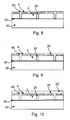
Figure 8 , anencapsulant 80 is deposited over the major surface of thewafer 30 comprising thesingulated substrates 2. Theencapsulant 80 covers themajor surface 3 of eachsingulated semiconductor substrate 2 and also may fill thesaw lanes 24. Note that theencapsulant 80 filling thesaw lanes 24 may subsequently form the part of theencapsulant 8 that covers theside walls 5 of eachsemiconductor substrate 2 of the kind described above. - In a next step shown in
Figure 9 , a number ofvias 26 may be formed through theencapsulant 80. As can be seen inFigure 9 , each via 26 may extend through a portion of theencapsulant 80 located substantially above eachcontact 4. Thevias 26 may, for example, be formed using a laser, whereby the location, size and shape of each via 26 may be precisely controlled. As previously noted, thevias 26 may, for instance, be circular or oblong in cross section. - In a next step shown in
Figure 10 , each via 26 may be filled withmetal 22. Themetal 22 may be deposited as a stack of metal layers as described above in relation to Table 1. - In a next step shown in
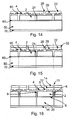
Figure 11 , themetal 22 may be patterned to produce a number of separate metal portions separated bygaps 28. Thesegaps 28 will, after singulation, correspond to thegaps 28 shown inFigures 2 and4 of the examples described above. - In a next step shown in
Figure 12 , themetal 22 may be covered with afurther metal layer 32 that, after singulation, will form thebond pads 14 of the kind described above in relation toFigures 1-4 . - In a next step shown in
Figure 13 , the wafer may be singulated along the dotted lines shown inFigure 12 , to produce a plurality ofsemiconductor devices 10 of the kind shown inFigures 1 and 2 . Note that the saw lanes used to singulate the wafer may be thinner than thesaw lanes 24 described above in relation toFigure 7 and may thus be sufficiently thin such that at least a part of theencapsulant 80 remains on the side walls of eachsemiconductor substrate 2, as already described in relation toFigure 1 and Figure 2 . -
Figures 14-16 show an alternative sequence of manufacturing steps to those described above in relation toFigures 11-13 . The sequence shown inFigures 14-16 is substantially the same as the sequence shown inFigures 11-13 , except that acoating 70 is provided on the back side of thesecond wafer 50. As can be seen inFigure 16 , after singulation, thecoating 70 forms acoating 16 on the back side of eachsecond substrate 20 of eachsingulated semiconductor device 10. Thecoating 16 may be a coating of the kind already described above in relation toFigures 3 and 4 . - Accordingly, there has been described a semiconductor device and a method of making the same. The device includes a semiconductor substrate having a major surface, one or more contacts located on the major surface and an encapsulant covering at least the major surface. A peripheral edge of each contact defines a contact area on the major surface. The device also includes one or more bond pads located outside the encapsulant. Each bond pad is electrically connected to a respective contact located on the major surface of the substrate by a respective metal filled via that passes through the encapsulant. A sidewall of each respective metal filled via, at the point at which it meets the respective contact, falls inside the contact area defined by the respective contact when viewed from above the major surface of the substrate, whereby none of the metal filling each respective via extends outside the contact area of each respective contact.
- Although particular embodiments of this disclosure have been described, it will be appreciated that many modifications/additions and/or substitutions may be made within the scope of the claims.
Claims (15)
- A semiconductor device comprising:a semiconductor substrate having a major surface;an encapsulant covering at least the major surface of the substrate;one or more contacts located on the major surface, wherein a peripheral edge of each contact defines a contact area on the major surface; andone or more bond pads located outside the encapsulant,wherein each bond pad is electrically connected to a respective contact located on the major surface of the substrate by a respective metal filled via that passes through the encapsulant, andwherein a sidewall of each respective metal filled via, at the point at which it meets the respective contact, falls inside the contact area defined by the respective contact when viewed from above the major surface of the substrate, whereby none of the metal filling each respective via extends outside the contact area of each respective contact.
- The semiconductor device of claim 1, wherein a surface area of each bond pad is larger than the contact area of the contact on the major surface of the substrate to which the bond pad is electrically connected.
- The semiconductor device of claim 1 or claim 2, wherein the encapsulant has a first outer surface located in a plane parallel to the major surface of the substrate, wherein the one or more bond pads are located on the first outer surface of the encapsulant.
- The semiconductor device of claim 3, wherein at least a part of a peripheral edge of at least some of the bond pads extends to an edge of the first outer surface.
- The semiconductor device of claim 3 or claim 4, wherein the metal of the metal filled vias extends at least partially over the first outer surface of the encapsulant.
- The semiconductor device of any preceding claim, wherein each bond pad completely covers an upper surface of the metal of the respective metal filled via electrically connecting the bond pad to the respective contact on the major surface of the substrate.
- The semiconductor device of any preceding claim, wherein the substrate has a backside and a plurality of sidewalls extending between the major surface and the backside, and wherein the encapsulant covers at least some of the sidewalls of the substrate.
- The semiconductor device of any preceding claim, wherein the substrate has a backside and a plurality of sidewalls extending between the major surface and the backside, and wherein the device further comprises a second substrate attached to the backside of the substrate.
- The semiconductor device of claim 8, wherein the second substrate has a major surface and a backside, wherein the major surface of the second substrate is attached to the backside of the semiconductor substrate, and wherein the backside of the second substrate is provided with a coating.
- A mobile communications device comprising the semiconductor device of any preceding claim.
- A method of making a semiconductor device, the method comprising:providing a semiconductor substrate having a major surface;forming one or more contacts located on the major surface, wherein a peripheral edge of each contact defines a contact area on the major surface;depositing an encapsulant to cover at least the major surface of the substrate;forming a via through the encapsulant for each respective contact on the major surface, wherein a sidewall of each via, at the point at which it meets the respective contact, falls inside the contact area defined by the respective contact when viewed from above the major surface of the substrate;filling each via with metal, wherein none of the metal filling each via extends outside the contact area of each respective contact; andfonning one or more bond pads located outside the encapsulant, wherein each bond pad is electrically connected to a respective contact located on the major surface of the substrate by a respective via filled with metal.
- The method of claim 11, comprising using a laser to form each respective via.
- The method of claim 11 or claim 12, comprising:providing a semiconductor wafer having a major surface corresponding to the major surface of said semiconductor substrate;forming said one or more contacts on the major surface of the wafer;depositing the encapsulant on the major surface of the wafer;forming said via(s) and filling each via with metal;forming said one or more bond pads; andsingulating the wafer to produce said semiconductor device.
- The method of claim 13, further comprising attaching a second wafer to a backside of the semiconductor wafer prior to said singulation.
- The method of claim 14, comprising sawing through the semiconductor wafer along a plurality of saw lanes after said semiconductor wafer is attached to the second wafer and prior to depositing the encapsulant, whereby the encapsulant fills the saw lanes to cover sidewalls of the semiconductor substrate formed by the sides of each saw lane.
Priority Applications (3)
| Application Number | Priority Date | Filing Date | Title |
|---|---|---|---|
| EP15194136.6A EP3168870A1 (en) | 2015-11-11 | 2015-11-11 | Semiconductor device and method of making a semiconductor device |
| US15/336,774 US9947632B2 (en) | 2015-11-11 | 2016-10-27 | Semiconductor device and method of making a semiconductor device |
| CN201610984517.8A CN107017222B (en) | 2015-11-11 | 2016-11-09 | Semiconductor device and method of manufacturing semiconductor device |
Applications Claiming Priority (1)
| Application Number | Priority Date | Filing Date | Title |
|---|---|---|---|
| EP15194136.6A EP3168870A1 (en) | 2015-11-11 | 2015-11-11 | Semiconductor device and method of making a semiconductor device |
Publications (1)
| Publication Number | Publication Date |
|---|---|
| EP3168870A1 true EP3168870A1 (en) | 2017-05-17 |
Family
ID=54540929
Family Applications (1)
| Application Number | Title | Priority Date | Filing Date |
|---|---|---|---|
| EP15194136.6A Ceased EP3168870A1 (en) | 2015-11-11 | 2015-11-11 | Semiconductor device and method of making a semiconductor device |
Country Status (3)
| Country | Link |
|---|---|
| US (1) | US9947632B2 (en) |
| EP (1) | EP3168870A1 (en) |
| CN (1) | CN107017222B (en) |
Families Citing this family (1)
| Publication number | Priority date | Publication date | Assignee | Title |
|---|---|---|---|---|
| EP3499552A1 (en) * | 2017-12-14 | 2019-06-19 | Nexperia B.V. | Semiconductor device and method of manufacture |
Citations (9)
| Publication number | Priority date | Publication date | Assignee | Title |
|---|---|---|---|---|
| US20090227070A1 (en) * | 2008-03-07 | 2009-09-10 | Denso Corporation | Semiconductor device and method of manufacturing the same |
| US20120211892A1 (en) * | 2011-02-22 | 2012-08-23 | Stats Chippac, Ltd. | Semiconductor Device and Method of Forming WLCSP Structure Using Protruded MLP |
| US20130032944A1 (en) * | 2011-08-01 | 2013-02-07 | Tessera, Inc. | Microelectronic package with stacked microelectronic elements and method for manufacture thereof |
| US20130040423A1 (en) * | 2011-08-10 | 2013-02-14 | Taiwan Semiconductor Manufacturing Company, Ltd. | Method of Multi-Chip Wafer Level Packaging |
| US20130037962A1 (en) * | 2011-08-09 | 2013-02-14 | Yan Xun Xue | Wafer level packaging structure with large contact area and preparation method thereof |
| US20130267066A1 (en) * | 2010-11-01 | 2013-10-10 | Samsung Electronics Co., Ltd. | Semiconductor Packages and Methods of Fabricating the Same |
| US20130334683A1 (en) * | 2012-06-13 | 2013-12-19 | SK Hynix Inc. | Electronic device packages having bumps and methods of manufacturing the same |
| US20140008809A1 (en) * | 2011-12-30 | 2014-01-09 | Deca Technologies, Inc. | Die up fully molded fan-out wafer level packaging |
| US9040316B1 (en) * | 2014-06-12 | 2015-05-26 | Deca Technologies Inc. | Semiconductor device and method of adaptive patterning for panelized packaging with dynamic via clipping |
Family Cites Families (2)
| Publication number | Priority date | Publication date | Assignee | Title |
|---|---|---|---|---|
| CN100342526C (en) * | 2003-08-22 | 2007-10-10 | 全懋精密科技股份有限公司 | Semiconductor packaging substrate structure with metal protective layer for electrical connection pads and its manufacturing method |
| US20090170241A1 (en) * | 2007-12-26 | 2009-07-02 | Stats Chippac, Ltd. | Semiconductor Device and Method of Forming the Device Using Sacrificial Carrier |
-
2015
- 2015-11-11 EP EP15194136.6A patent/EP3168870A1/en not_active Ceased
-
2016
- 2016-10-27 US US15/336,774 patent/US9947632B2/en active Active
- 2016-11-09 CN CN201610984517.8A patent/CN107017222B/en active Active
Patent Citations (9)
| Publication number | Priority date | Publication date | Assignee | Title |
|---|---|---|---|---|
| US20090227070A1 (en) * | 2008-03-07 | 2009-09-10 | Denso Corporation | Semiconductor device and method of manufacturing the same |
| US20130267066A1 (en) * | 2010-11-01 | 2013-10-10 | Samsung Electronics Co., Ltd. | Semiconductor Packages and Methods of Fabricating the Same |
| US20120211892A1 (en) * | 2011-02-22 | 2012-08-23 | Stats Chippac, Ltd. | Semiconductor Device and Method of Forming WLCSP Structure Using Protruded MLP |
| US20130032944A1 (en) * | 2011-08-01 | 2013-02-07 | Tessera, Inc. | Microelectronic package with stacked microelectronic elements and method for manufacture thereof |
| US20130037962A1 (en) * | 2011-08-09 | 2013-02-14 | Yan Xun Xue | Wafer level packaging structure with large contact area and preparation method thereof |
| US20130040423A1 (en) * | 2011-08-10 | 2013-02-14 | Taiwan Semiconductor Manufacturing Company, Ltd. | Method of Multi-Chip Wafer Level Packaging |
| US20140008809A1 (en) * | 2011-12-30 | 2014-01-09 | Deca Technologies, Inc. | Die up fully molded fan-out wafer level packaging |
| US20130334683A1 (en) * | 2012-06-13 | 2013-12-19 | SK Hynix Inc. | Electronic device packages having bumps and methods of manufacturing the same |
| US9040316B1 (en) * | 2014-06-12 | 2015-05-26 | Deca Technologies Inc. | Semiconductor device and method of adaptive patterning for panelized packaging with dynamic via clipping |
Also Published As
| Publication number | Publication date |
|---|---|
| CN107017222B (en) | 2021-10-19 |
| US9947632B2 (en) | 2018-04-17 |
| US20170133335A1 (en) | 2017-05-11 |
| CN107017222A (en) | 2017-08-04 |
Similar Documents
| Publication | Publication Date | Title |
|---|---|---|
| US12166001B2 (en) | Single-shot encapsulation | |
| TWI778381B (en) | A semiconductor device with an electromagnetic interference (emi) shield | |
| TWI725262B (en) | Semiconductor device and method of forming a 3d interposer system-in-package module | |
| US8247269B1 (en) | Wafer level embedded and stacked die power system-in-package packages | |
| US9312218B2 (en) | Semiconductor device and method of forming leadframe with conductive bodies for vertical electrical interconnect of semiconductor die | |
| US10804217B2 (en) | EMI shielding for flip chip package with exposed die backside | |
| US11145588B2 (en) | Method for fabricating semiconductor package and semiconductor package using the same | |
| US20110037155A1 (en) | Semiconductor Device and Method of Forming Dam Material Around Periphery of Die to Reduce Warpage | |
| TWI861546B (en) | Package with windowed heat spreader | |
| US9418942B2 (en) | Semiconductor device | |
| US20120286410A1 (en) | Semiconductor device packaging method and semiconductor device package | |
| US9263335B2 (en) | Discrete semiconductor device package and manufacturing method | |
| KR101631406B1 (en) | Semiconductor package and manufacturing method thereof | |
| US7109587B1 (en) | Apparatus and method for enhanced thermal conductivity packages for high powered semiconductor devices | |
| TWI862968B (en) | Package with compartmentalized lid for heat spreader and emi shield | |
| US9947632B2 (en) | Semiconductor device and method of making a semiconductor device | |
| TW202349643A (en) | Semiconductor device and method of selective shielding using fod material | |
| TW202331861A (en) | Semiconductor device and method of forming selective emi shielding with slotted substrate | |
| TW202505710A (en) | Semiconductor device and method of forming an antenna-in-package structure | |
| KR20240164743A (en) | Semiconductor device and method of making a dual-side molded system-in-package with fine-pitched interconnects | |
| JP2009295646A (en) | Chip size package semiconductor device and method of manufacturing the same |
Legal Events
| Date | Code | Title | Description |
|---|---|---|---|
| PUAI | Public reference made under article 153(3) epc to a published international application that has entered the european phase |
Free format text: ORIGINAL CODE: 0009012 |
|
| STAA | Information on the status of an ep patent application or granted ep patent |
Free format text: STATUS: THE APPLICATION HAS BEEN PUBLISHED |
|
| AK | Designated contracting states |
Kind code of ref document: A1 Designated state(s): AL AT BE BG CH CY CZ DE DK EE ES FI FR GB GR HR HU IE IS IT LI LT LU LV MC MK MT NL NO PL PT RO RS SE SI SK SM TR |
|
| AX | Request for extension of the european patent |
Extension state: BA ME |
|
| STAA | Information on the status of an ep patent application or granted ep patent |
Free format text: STATUS: REQUEST FOR EXAMINATION WAS MADE |
|
| 17P | Request for examination filed |
Effective date: 20171113 |
|
| RBV | Designated contracting states (corrected) |
Designated state(s): AL AT BE BG CH CY CZ DE DK EE ES FI FR GB GR HR HU IE IS IT LI LT LU LV MC MK MT NL NO PL PT RO RS SE SI SK SM TR |
|
| STAA | Information on the status of an ep patent application or granted ep patent |
Free format text: STATUS: EXAMINATION IS IN PROGRESS |
|
| 17Q | First examination report despatched |
Effective date: 20200127 |
|
| RAP3 | Party data changed (applicant data changed or rights of an application transferred) |
Owner name: NEXPERIA B.V. |
|
| 18R | Application refused |
Effective date: 20240222 |