EP3168677A1 - Double-surface display panel and double-surface display apparatus - Google Patents
Double-surface display panel and double-surface display apparatus Download PDFInfo
- Publication number
- EP3168677A1 EP3168677A1 EP14882144.0A EP14882144A EP3168677A1 EP 3168677 A1 EP3168677 A1 EP 3168677A1 EP 14882144 A EP14882144 A EP 14882144A EP 3168677 A1 EP3168677 A1 EP 3168677A1
- Authority
- EP
- European Patent Office
- Prior art keywords
- sub
- display
- unit
- double
- faced
- Prior art date
- Legal status (The legal status is an assumption and is not a legal conclusion. Google has not performed a legal analysis and makes no representation as to the accuracy of the status listed.)
- Granted
Links
Images

Classifications
-
- H—ELECTRICITY
- H10—SEMICONDUCTOR DEVICES; ELECTRIC SOLID-STATE DEVICES NOT OTHERWISE PROVIDED FOR
- H10K—ORGANIC ELECTRIC SOLID-STATE DEVICES
- H10K59/00—Integrated devices, or assemblies of multiple devices, comprising at least one organic light-emitting element covered by group H10K50/00
- H10K59/10—OLED displays
- H10K59/12—Active-matrix OLED [AMOLED] displays
- H10K59/128—Active-matrix OLED [AMOLED] displays comprising two independent displays, e.g. for emitting information from two major sides of the display
-
- G—PHYSICS
- G02—OPTICS
- G02F—OPTICAL DEVICES OR ARRANGEMENTS FOR THE CONTROL OF LIGHT BY MODIFICATION OF THE OPTICAL PROPERTIES OF THE MEDIA OF THE ELEMENTS INVOLVED THEREIN; NON-LINEAR OPTICS; FREQUENCY-CHANGING OF LIGHT; OPTICAL LOGIC ELEMENTS; OPTICAL ANALOGUE/DIGITAL CONVERTERS
- G02F1/00—Devices or arrangements for the control of the intensity, colour, phase, polarisation or direction of light arriving from an independent light source, e.g. switching, gating or modulating; Non-linear optics
- G02F1/01—Devices or arrangements for the control of the intensity, colour, phase, polarisation or direction of light arriving from an independent light source, e.g. switching, gating or modulating; Non-linear optics for the control of the intensity, phase, polarisation or colour
- G02F1/13—Devices or arrangements for the control of the intensity, colour, phase, polarisation or direction of light arriving from an independent light source, e.g. switching, gating or modulating; Non-linear optics for the control of the intensity, phase, polarisation or colour based on liquid crystals, e.g. single liquid crystal display cells
- G02F1/133—Constructional arrangements; Operation of liquid crystal cells; Circuit arrangements
- G02F1/1333—Constructional arrangements; Manufacturing methods
- G02F1/1343—Electrodes
- G02F1/134309—Electrodes characterised by their geometrical arrangement
-
- G—PHYSICS
- G02—OPTICS
- G02F—OPTICAL DEVICES OR ARRANGEMENTS FOR THE CONTROL OF LIGHT BY MODIFICATION OF THE OPTICAL PROPERTIES OF THE MEDIA OF THE ELEMENTS INVOLVED THEREIN; NON-LINEAR OPTICS; FREQUENCY-CHANGING OF LIGHT; OPTICAL LOGIC ELEMENTS; OPTICAL ANALOGUE/DIGITAL CONVERTERS
- G02F1/00—Devices or arrangements for the control of the intensity, colour, phase, polarisation or direction of light arriving from an independent light source, e.g. switching, gating or modulating; Non-linear optics
- G02F1/01—Devices or arrangements for the control of the intensity, colour, phase, polarisation or direction of light arriving from an independent light source, e.g. switching, gating or modulating; Non-linear optics for the control of the intensity, phase, polarisation or colour
- G02F1/13—Devices or arrangements for the control of the intensity, colour, phase, polarisation or direction of light arriving from an independent light source, e.g. switching, gating or modulating; Non-linear optics for the control of the intensity, phase, polarisation or colour based on liquid crystals, e.g. single liquid crystal display cells
- G02F1/133—Constructional arrangements; Operation of liquid crystal cells; Circuit arrangements
- G02F1/1333—Constructional arrangements; Manufacturing methods
- G02F1/1343—Electrodes
- G02F1/13439—Electrodes characterised by their electrical, optical, physical properties; materials therefor; method of making
-
- G—PHYSICS
- G02—OPTICS
- G02F—OPTICAL DEVICES OR ARRANGEMENTS FOR THE CONTROL OF LIGHT BY MODIFICATION OF THE OPTICAL PROPERTIES OF THE MEDIA OF THE ELEMENTS INVOLVED THEREIN; NON-LINEAR OPTICS; FREQUENCY-CHANGING OF LIGHT; OPTICAL LOGIC ELEMENTS; OPTICAL ANALOGUE/DIGITAL CONVERTERS
- G02F1/00—Devices or arrangements for the control of the intensity, colour, phase, polarisation or direction of light arriving from an independent light source, e.g. switching, gating or modulating; Non-linear optics
- G02F1/01—Devices or arrangements for the control of the intensity, colour, phase, polarisation or direction of light arriving from an independent light source, e.g. switching, gating or modulating; Non-linear optics for the control of the intensity, phase, polarisation or colour
- G02F1/13—Devices or arrangements for the control of the intensity, colour, phase, polarisation or direction of light arriving from an independent light source, e.g. switching, gating or modulating; Non-linear optics for the control of the intensity, phase, polarisation or colour based on liquid crystals, e.g. single liquid crystal display cells
- G02F1/137—Devices or arrangements for the control of the intensity, colour, phase, polarisation or direction of light arriving from an independent light source, e.g. switching, gating or modulating; Non-linear optics for the control of the intensity, phase, polarisation or colour based on liquid crystals, e.g. single liquid crystal display cells characterised by the electro-optical or magneto-optical effect, e.g. field-induced phase transition, orientation effect, guest-host interaction or dynamic scattering
-
- G—PHYSICS
- G02—OPTICS
- G02F—OPTICAL DEVICES OR ARRANGEMENTS FOR THE CONTROL OF LIGHT BY MODIFICATION OF THE OPTICAL PROPERTIES OF THE MEDIA OF THE ELEMENTS INVOLVED THEREIN; NON-LINEAR OPTICS; FREQUENCY-CHANGING OF LIGHT; OPTICAL LOGIC ELEMENTS; OPTICAL ANALOGUE/DIGITAL CONVERTERS
- G02F1/00—Devices or arrangements for the control of the intensity, colour, phase, polarisation or direction of light arriving from an independent light source, e.g. switching, gating or modulating; Non-linear optics
- G02F1/01—Devices or arrangements for the control of the intensity, colour, phase, polarisation or direction of light arriving from an independent light source, e.g. switching, gating or modulating; Non-linear optics for the control of the intensity, phase, polarisation or colour
- G02F1/13—Devices or arrangements for the control of the intensity, colour, phase, polarisation or direction of light arriving from an independent light source, e.g. switching, gating or modulating; Non-linear optics for the control of the intensity, phase, polarisation or colour based on liquid crystals, e.g. single liquid crystal display cells
- G02F1/137—Devices or arrangements for the control of the intensity, colour, phase, polarisation or direction of light arriving from an independent light source, e.g. switching, gating or modulating; Non-linear optics for the control of the intensity, phase, polarisation or colour based on liquid crystals, e.g. single liquid crystal display cells characterised by the electro-optical or magneto-optical effect, e.g. field-induced phase transition, orientation effect, guest-host interaction or dynamic scattering
- G02F1/139—Devices or arrangements for the control of the intensity, colour, phase, polarisation or direction of light arriving from an independent light source, e.g. switching, gating or modulating; Non-linear optics for the control of the intensity, phase, polarisation or colour based on liquid crystals, e.g. single liquid crystal display cells characterised by the electro-optical or magneto-optical effect, e.g. field-induced phase transition, orientation effect, guest-host interaction or dynamic scattering based on orientation effects in which the liquid crystal remains transparent
- G02F1/1396—Devices or arrangements for the control of the intensity, colour, phase, polarisation or direction of light arriving from an independent light source, e.g. switching, gating or modulating; Non-linear optics for the control of the intensity, phase, polarisation or colour based on liquid crystals, e.g. single liquid crystal display cells characterised by the electro-optical or magneto-optical effect, e.g. field-induced phase transition, orientation effect, guest-host interaction or dynamic scattering based on orientation effects in which the liquid crystal remains transparent the liquid crystal being selectively controlled between a twisted state and a non-twisted state, e.g. TN-LC cell
-
- H—ELECTRICITY
- H10—SEMICONDUCTOR DEVICES; ELECTRIC SOLID-STATE DEVICES NOT OTHERWISE PROVIDED FOR
- H10K—ORGANIC ELECTRIC SOLID-STATE DEVICES
- H10K50/00—Organic light-emitting devices
- H10K50/80—Constructional details
- H10K50/85—Arrangements for extracting light from the devices
- H10K50/856—Arrangements for extracting light from the devices comprising reflective means
-
- H—ELECTRICITY
- H10—SEMICONDUCTOR DEVICES; ELECTRIC SOLID-STATE DEVICES NOT OTHERWISE PROVIDED FOR
- H10K—ORGANIC ELECTRIC SOLID-STATE DEVICES
- H10K59/00—Integrated devices, or assemblies of multiple devices, comprising at least one organic light-emitting element covered by group H10K50/00
- H10K59/30—Devices specially adapted for multicolour light emission
- H10K59/35—Devices specially adapted for multicolour light emission comprising red-green-blue [RGB] subpixels
-
- H—ELECTRICITY
- H10—SEMICONDUCTOR DEVICES; ELECTRIC SOLID-STATE DEVICES NOT OTHERWISE PROVIDED FOR
- H10K—ORGANIC ELECTRIC SOLID-STATE DEVICES
- H10K59/00—Integrated devices, or assemblies of multiple devices, comprising at least one organic light-emitting element covered by group H10K50/00
- H10K59/50—OLEDs integrated with light modulating elements, e.g. with electrochromic elements, photochromic elements or liquid crystal elements
-
- H—ELECTRICITY
- H10—SEMICONDUCTOR DEVICES; ELECTRIC SOLID-STATE DEVICES NOT OTHERWISE PROVIDED FOR
- H10K—ORGANIC ELECTRIC SOLID-STATE DEVICES
- H10K59/00—Integrated devices, or assemblies of multiple devices, comprising at least one organic light-emitting element covered by group H10K50/00
- H10K59/80—Constructional details
- H10K59/875—Arrangements for extracting light from the devices
- H10K59/878—Arrangements for extracting light from the devices comprising reflective means
-
- H—ELECTRICITY
- H10—SEMICONDUCTOR DEVICES; ELECTRIC SOLID-STATE DEVICES NOT OTHERWISE PROVIDED FOR
- H10K—ORGANIC ELECTRIC SOLID-STATE DEVICES
- H10K59/00—Integrated devices, or assemblies of multiple devices, comprising at least one organic light-emitting element covered by group H10K50/00
- H10K59/90—Assemblies of multiple devices comprising at least one organic light-emitting element
-
- G—PHYSICS
- G02—OPTICS
- G02F—OPTICAL DEVICES OR ARRANGEMENTS FOR THE CONTROL OF LIGHT BY MODIFICATION OF THE OPTICAL PROPERTIES OF THE MEDIA OF THE ELEMENTS INVOLVED THEREIN; NON-LINEAR OPTICS; FREQUENCY-CHANGING OF LIGHT; OPTICAL LOGIC ELEMENTS; OPTICAL ANALOGUE/DIGITAL CONVERTERS
- G02F1/00—Devices or arrangements for the control of the intensity, colour, phase, polarisation or direction of light arriving from an independent light source, e.g. switching, gating or modulating; Non-linear optics
- G02F1/01—Devices or arrangements for the control of the intensity, colour, phase, polarisation or direction of light arriving from an independent light source, e.g. switching, gating or modulating; Non-linear optics for the control of the intensity, phase, polarisation or colour
- G02F1/13—Devices or arrangements for the control of the intensity, colour, phase, polarisation or direction of light arriving from an independent light source, e.g. switching, gating or modulating; Non-linear optics for the control of the intensity, phase, polarisation or colour based on liquid crystals, e.g. single liquid crystal display cells
- G02F1/133—Constructional arrangements; Operation of liquid crystal cells; Circuit arrangements
- G02F1/1333—Constructional arrangements; Manufacturing methods
- G02F1/133342—Constructional arrangements; Manufacturing methods for double-sided displays
-
- G—PHYSICS
- G02—OPTICS
- G02F—OPTICAL DEVICES OR ARRANGEMENTS FOR THE CONTROL OF LIGHT BY MODIFICATION OF THE OPTICAL PROPERTIES OF THE MEDIA OF THE ELEMENTS INVOLVED THEREIN; NON-LINEAR OPTICS; FREQUENCY-CHANGING OF LIGHT; OPTICAL LOGIC ELEMENTS; OPTICAL ANALOGUE/DIGITAL CONVERTERS
- G02F2201/00—Constructional arrangements not provided for in groups G02F1/00 - G02F7/00
- G02F2201/44—Arrangements combining different electro-active layers, e.g. electrochromic, liquid crystal or electroluminescent layers
-
- G—PHYSICS
- G02—OPTICS
- G02F—OPTICAL DEVICES OR ARRANGEMENTS FOR THE CONTROL OF LIGHT BY MODIFICATION OF THE OPTICAL PROPERTIES OF THE MEDIA OF THE ELEMENTS INVOLVED THEREIN; NON-LINEAR OPTICS; FREQUENCY-CHANGING OF LIGHT; OPTICAL LOGIC ELEMENTS; OPTICAL ANALOGUE/DIGITAL CONVERTERS
- G02F2203/00—Function characteristic
- G02F2203/01—Function characteristic transmissive
-
- G—PHYSICS
- G02—OPTICS
- G02F—OPTICAL DEVICES OR ARRANGEMENTS FOR THE CONTROL OF LIGHT BY MODIFICATION OF THE OPTICAL PROPERTIES OF THE MEDIA OF THE ELEMENTS INVOLVED THEREIN; NON-LINEAR OPTICS; FREQUENCY-CHANGING OF LIGHT; OPTICAL LOGIC ELEMENTS; OPTICAL ANALOGUE/DIGITAL CONVERTERS
- G02F2203/00—Function characteristic
- G02F2203/02—Function characteristic reflective
-
- H—ELECTRICITY
- H10—SEMICONDUCTOR DEVICES; ELECTRIC SOLID-STATE DEVICES NOT OTHERWISE PROVIDED FOR
- H10K—ORGANIC ELECTRIC SOLID-STATE DEVICES
- H10K2102/00—Constructional details relating to the organic devices covered by this subclass
- H10K2102/301—Details of OLEDs
- H10K2102/302—Details of OLEDs of OLED structures
- H10K2102/3023—Direction of light emission
- H10K2102/3026—Top emission
-
- H—ELECTRICITY
- H10—SEMICONDUCTOR DEVICES; ELECTRIC SOLID-STATE DEVICES NOT OTHERWISE PROVIDED FOR
- H10K—ORGANIC ELECTRIC SOLID-STATE DEVICES
- H10K2102/00—Constructional details relating to the organic devices covered by this subclass
- H10K2102/301—Details of OLEDs
- H10K2102/302—Details of OLEDs of OLED structures
- H10K2102/3023—Direction of light emission
- H10K2102/3031—Two-side emission, e.g. transparent OLEDs [TOLED]
Definitions
- Embodiments of the invention relate to a double-faced display panel and a double-faced display device comprising the double-faced display panel.
- Double-faced display has many advantages, for example, when the double-faced display device is adopted as a television signal receiving device at home, it can be embedded into a door frame or partition wall of adjacent rooms, so persons in different rooms can acquire one piece or different pieces of information at the same time.
- the double-faced display device has problems of low light utilization, small contrast between display brightness and ambient light, difficulty in recognizing a display picture under bright light and the like.
- Embodiments of the invention provide a double-faced display panel and a double-faced display device comprising the double-faced display panel, which has higher light utilization, improves contrast between display brightness and ambient light and has a better display effect.
- an embodiment of the invention provides a double-faced display panel, comprising: a first display sub-unit, provided with a first display surface and a first non-display surface opposite to each other; a second display sub-unit, provided with a second display surface and a second non-display surface opposite to each other, and arranged back to back with the first display sub-unit, the second non-display surface facing the first non-display surface; and a reflection unit, arranged between the first display sub-unit and the second display sub-unit, wherein the reflection unit is configured to reflect displaying light emitted from the first display sub-unit back to the first display sub-unit and reflect displaying light emitted from the second display sub-unit back to the second display sub-unit.
- an embodiment of the invention further provides a double-faced display device, comprising: a display panel, which is the double-faced display panel described above; and a drive circuit, connected with the display panel.
- the first embodiment of the invention provides a double-faced display panel; as shown in FIG. 1 , the double-faced display panel comprises: a first display sub-unit 1, provided with a first display surface and a first non-display surface opposite to each other; a second display sub-unit 2, provided with a second display surface and a second non-display surface opposite to each other, the second display sub-unit 2 being arranged back to back with the first display sub-unit 1, and the second non-display surface facing the first non-display surface; and a reflection unit 3, arranged between the first display sub-unit 1 and the second display sub-unit 2, and configured to reflect display light emitted from the first display sub-unit 1 back to the first display sub-unit 1 and reflect display light emitted from the second display sub-unit 2 back to the second display sub-unit 2.
- the first display sub-unit 1 includes two first substrates 11 oppositely arranged and a plurality of first sub-pixels 12 arranged between the two first substrates 11;
- the second display sub-unit 2 includes two second substrates 21 oppositely arranged and a plurality of second sub-pixels 22 arranged between the two second substrates 21.
- the reflection unit 3 is configured to reflect the light emitted from the first sub-pixels 12 back to the first display sub-unit 1 and reflect the light emitted from second sub-pixels 22 back to the second display sub-unit 2.
- each of the first sub-pixels 12 and the second sub-pixels 22 includes an Organic Light-Emitting Diode (OLED), wherein the OLED may be of a top emitting type or a double directional emitting type.
- OLED Organic Light-Emitting Diode
- the OLED included by each of the first sub-pixels 12 and the second sub-pixels 22 is of the top emitting type, namely, each OLED of the first sub-pixels 12 and each OLED of the second sub-pixels 22 respectively emit light to the display surfaces disposed back to back of the first display sub-unit and the second display sub-unit
- the reflection unit 3 can reflect the light deflected and emitted to the non-display surfaces back to the first display sub-unit and the second display sub-unit, thus improving the light utilization.
- each OLED included by each of the first sub-pixels 12 and the second sub-pixels 22 is the double directional emitting type
- one OLED can not only emit light to the top, but also emit light to the bottom (i.e., a side facing the reflection unit 3)
- the light emitted to the top can directly be transmitted through the first display sub-unit 1 or the second display sub-unit 2 for use, and the light emitted to the bottom is reflected by the reflection unit 3 and then be transmitted through the first display sub-unit 1 or the second display sub-unit 2 for use, thus improving the light utilization of the double-faced display panel.
- a structure of each OLED included by each of the first sub-pixels 12 and the second sub-pixels 22 may include three layers: an anode, a light emitting layer and a cathode, for example, FIG. 3 shows the structure of the OLED included by the first sub-pixel 12, comprising: an anode 121, a cathode 123 and a light emitting layer 122 arranged between the anode 121 and the cathode 123.
- the OLED may further include an organic functional layer arranged between the anode 121 and the cathode 123, and the organic functional layer includes at least one of a hole injection layer, a hole transport layer, an electron blocking layer, a hole and exciton blocking layer, an electron transport layer and an electron injection layer.
- the organic functional layer may be flexibly selected according to needs in actual application, which will not be repeated herein.
- an electrode arranged close to the display surface of the first or second display sub-unit may be an anode or a cathode, but is a transparent electrode, correspondingly, the other electrode except the electrode close to the display surface may be a non-transparent electrode or a reflection electrode; for the OLED of double directional emitting type, at least one of the cathode or the anode is transparent.
- the first sub-pixels 21 may include first sub-pixels with three colors of red (R), green (G) and blue (B), and the second sub-pixels 22 may also include second sub pixels with three colors of red (R), green (G) and blue (B), that is to say, color display is realized in a full color manner.
- each of the first sub-pixels and the second sub-pixels may include a white OLED, and RGB color filters are arranged on the substrates at a light exitting side, so the full color display is realized in a WOLED-COA manner; of course, the color display may be realized in a WOLED-CF (a white OLED and four color filters of R, G, B, W) manner, which is not limited by the embodiment of the invention.
- the reflection unit 3 includes a switch layer 33 and a first reflection layer 31 and a second reflection layer 32 which are respectively complementarily arranged on both sides of the switch layer 33 in a staggered manner.
- the first reflection layer 31 and the second reflection layer 32 may be a reflection mirror, for example, a chemically silvered silver mirror.
- the first reflection layer 31 is disposed to correspond to the first sub-pixels 12 and is separated from the first display sub-unit 1 by the second reflection layer 32 and the switch layer 33
- the second reflection layer 32 is disposed to correspond to the second sub-pixels 22 and is separated from the second display sub-unit 2 by the first reflection layer 31 and the switch layer 33
- the first reflection layer 31 is arranged on a side of the switch layer 33 close to the second display sub-unit 2
- the second reflection layer 32 is arranged on a side of the switch layer 33 close to the first display sub-unit 1.
- the first reflection layer 31 and the second reflection layer 32 are arranged on both sides of the switch layer 33, “staggered” means that orthogonal projections of the first reflection layer 31 and the second reflection layer 32 do not overlap on the switch layer 33, and “complementarily” means that the first reflection layer 31 and the second reflection layer 32 can form a whole seamless pattern by parallel movement to the same plane.
- the switch layer 33 is mainly used for adjusting light to activate or deactivate reflection.
- the switch layer 33 includes a liquid crystal cell, the liquid crystal cell including an upper substrate 331, a lower substrate 333 and a liquid crystal layer 332 arranged between the upper substrate 331 and the lower substrate 333, wherein the liquid crystal cell further includes a control electrode, the control electrode including: a plurality of first upper electrodes 311 and second upper electrodes 321 which are alternately arranged at an interval on a side of the upper substrate 331 close to the liquid crystal layer 332, and a plurality of first lower electrodes 312 and second lower electrodes 322 which are alternately arranged at an interval on a side of the lower substrate 333 close to the liquid crystal layer 332, wherein the first upper electrodes 311 and the first lower electrodes 312 are arranged in pair and correspond to the first reflection layer 31, the second upper electrodes 321 and the second lower electrodes 322 are arranged in pair and correspond to the second reflection layer 32, the first upper electrodes 3
- the liquid crystal positioned between the first upper electrodes 311 and the first lower electrodes 312 in the liquid crystal cell deflects
- the second upper electrodes 321 and the second lower electrodes 322 are respectively applied with voltages with a voltage difference
- the liquid crystal positioned between the second upper electrodes 321 and the second lower electrodes 322 in the liquid crystal cell deflects.
- the plurality of first upper electrodes 311 may be applied with a same voltage
- the plurality of first lower electrodes 312 may be applied with a same voltage
- the plurality of second upper electrodes 321 may be applied with a same voltage
- the plurality of second lower electrodes 322 may be applied with a same voltage
- the first upper electrodes and the second upper electrodes are respectively controlled
- the first lower electrodes and the second lower electrodes are respectively controlled.
- the first upper electrodes 311 and the first lower electrodes 312 are respectively applied with a positive voltage and a reference voltage
- the second upper electrodes 321 and the second lower electrodes 322 are respectively applied with a positive voltage and a reference voltage, and in this way, an electric field is formed by applying a voltage to the control electrode, so that deflection of the liquid crystal can be conveniently controlled.
- control electrode may be made from transparent electrode material, for example, Indium Tin Oxide (ITO), and the liquid crystal in the liquid crystal cell sandwiched between two layers of sub-electrodes may be Twisted Nematic (TN) type liquid crystal; namely, the liquid crystal deflects to form a transparent state when an electric field is applied, and is in an non-transparent state when no electric field is applied.
- ITO Indium Tin Oxide
- TN Twisted Nematic
- a light control state of the reflection unit 3 is changed by controlling a magnitude of the electric field between the sub-electrodes.
- the switch layer 33 may be switched between two different optical states of the transparent state and the non-transparent state, so the reflection layer performs a function or not.
- the control electrode in a corresponding region is controlled to apply an electric field, liquid crystal molecules are regularly arranged perpendicular to the electric field, and refractive indexes of the liquid crystal molecules are matched to form the transparent state, so the reflection layer corresponding to the sub-pixel play a role, and light emitted by the transparent sub-pixel can be reflected, so as to achieve a highlight display effect and an energy-saving aim; as shown in FIG.
- the first display sub-unit 1 further includes first black matrixes (BM) 13 arranged between adjacent first sub-pixels 12
- the second display sub-unit 2 further includes second black matrixes 23 arranged between adjacent second sub-pixels 22,
- the first reflection layer 31 is disposed to correspond to the second black matrixes 23, and
- the second reflection layer 32 is disposed to correspond to the first black matrixes 13.
- the first reflection layer 31, the first sub-pixel 12 and the second black matrix 23 are same in area; and the second reflection layer 32, the second sub-pixel 22 and the first black matrix 13 are same in area.
- the sub-pixels in the first display sub-unit 1 and the second display sub-unit 2 are arranged in a staggering manner respectively, the first sub-pixels 12 of the first display sub-unit 1 correspond to the first reflection layer 31 and the second black matrixes 23 of the second display sub-unit 2, which not only effectively use light emitted by the first sub-pixels 12 in the first display sub-unit 1 to improve light utilization of the first display sub-unit 1, but also does not influence operation of the second display sub-unit 2; similarly, the second sub-pixels 22 of the second display sub-unit 2 correspond to the second reflection layer 32 and the first black matrixes 13 of the first display sub-unit 1, which not only effectively use light emitted by the second sub-pixels 22 in the second display sub-unit 2 to improve light utilization of the second display sub-unit 2, but also does not influence
- the areas of the first reflection layer 31, the first sub-pixel 12 and the second black matrix 23 may also be different, and the areas of the second reflection layer 32, the second sub-pixel 22 and the first black matrix 13 may also be different, as long as the operation of the second display sub-unit 2 and that of the first display sub-unit 1 do not affect each other and the light utilization can be improved, which is not limited by the embodiment of the invention.
- the first sub-pixel 12 and the second sub-pixel 22 are same in area.
- the areas of the first sub-pixel 12, the first black matrix 13 and the first reflection layer 31 in the first display sub-unit 1 are same as those of the second sub-pixel 22, the second black matrix 23 and the second reflection layer 32 in the second display sub-unit 2, in order to further simplify a design process and improve process efficiency.
- an embodiment of the invention further provides a manufacturing method of a double-faced display panel; when the above double-faced display panel is manufactured, the first display sub-unit 1, the second display sub-unit 2 and the reflection unit 3 may be manufactured respectively, then they are bonded with a sealant to form a whole; also one display sub-unit may be taken as a reference, and the reflection unit 3 and the other display sub-unit may be formed on one side of the display sub-unit in sequence.
- Step 1 manufacturing a sub-pixel including an OLED and a black matrix on a first base substrate, for example, a transparent substrate, and arranging a second base substrate opposite to the first base substrate, to form one display sub-unit.
- each sub-pixel may emit red (R), green (G) or blue (B) color light, and the black matrix and the sub pixel are same in area.
- Step 2 manufacturing a reflection layer at a position, corresponding to the black matrix, of the second base substrate at a non-display surface of the display sub-unit; and then forming a switch layer and the other switch layer on the reflection layer, wherein the positions of the two reflection layers are staggered and complementary;
- Step 3 arranging a third base substrate, for example a transparent substrate, on the other reflection layer, and then manufacturing a sub-pixel including an OLED and a black matrix on the third base substrate and arranging a fourth base substrate opposite to the third base substrate, to form the other display sub-unit.
- a third base substrate for example a transparent substrate
- OLED organic light-emitting diode
- a fourth base substrate opposite to the third base substrate
- the reflection unit can reflect displaying light emitted by each of the display sub-units and travelling to the non-display surface back to the corresponding display sub-unit for reuse, and can block ambient light, so that the double-faced display panel has higher display brightness and high contrast, the contrast between the display brightness of the display panel and the ambient light can be improved, a better display effect is achieved, and in addition, more energy is saved under the condition of the same display brightness.
- the second embodiment of the invention provides a double-faced display device, comprising a display panel and a drive circuit connected with the display panel, and the display panel is the double-faced display panel in the first embodiment.
- the first display sub-unit and the second display sub-unit have independent drive circuits, and the first display sub-unit and the second display sub-unit display same or different images at a certain moment.
- one assembly manner is: firstly bonding two first substrates 11 with a first sub-pixel 12 by a sealant to form a first display sub-unit 1; meanwhile, connecting two second substrates 21 with a second sub-pixel 22 by a sealant to form a second display sub-unit 2; then arranging a reflection unit 3 between the first display sub-unit 1 and the second display sub-unit 2, aligning them, and performing frame sealing by using a sealant, so as to obtain the double-faced display device.
- the double-faced display device has two independent input ports, through which same or different signals may be input; and correspondingly, same or different image information may be displayed.
- the double-faced display panel thereof adopts the reflection unit to reflect the light emitted from the sub-pixels in the first display sub-unit and the second display sub-unit and travelling to the non-display surface for reuse, the light utilization of the double-faced display device is improved, and highlight and better contrast are realized, so the display device has better display effect, and a viewer can easily recognize a picture even under bright light and obtain a better visual experience.
Landscapes
- Physics & Mathematics (AREA)
- Nonlinear Science (AREA)
- Optics & Photonics (AREA)
- General Physics & Mathematics (AREA)
- Crystallography & Structural Chemistry (AREA)
- Chemical & Material Sciences (AREA)
- Mathematical Physics (AREA)
- Engineering & Computer Science (AREA)
- Microelectronics & Electronic Packaging (AREA)
- Geometry (AREA)
- Devices For Indicating Variable Information By Combining Individual Elements (AREA)
- Liquid Crystal (AREA)
- Electroluminescent Light Sources (AREA)
Abstract
Description
- Embodiments of the invention relate to a double-faced display panel and a double-faced display device comprising the double-faced display panel.
- With diversified demands on a display function, a double-faced display device is widely adopted. Double-faced display has many advantages, for example, when the double-faced display device is adopted as a television signal receiving device at home, it can be embedded into a door frame or partition wall of adjacent rooms, so persons in different rooms can acquire one piece or different pieces of information at the same time.
- However, due to diversity of application environments, the double-faced display device has problems of low light utilization, small contrast between display brightness and ambient light, difficulty in recognizing a display picture under bright light and the like.
- Embodiments of the invention provide a double-faced display panel and a double-faced display device comprising the double-faced display panel, which has higher light utilization, improves contrast between display brightness and ambient light and has a better display effect.
- In one aspect, an embodiment of the invention provides a double-faced display panel, comprising: a first display sub-unit, provided with a first display surface and a first non-display surface opposite to each other; a second display sub-unit, provided with a second display surface and a second non-display surface opposite to each other, and arranged back to back with the first display sub-unit, the second non-display surface facing the first non-display surface; and a reflection unit, arranged between the first display sub-unit and the second display sub-unit, wherein the reflection unit is configured to reflect displaying light emitted from the first display sub-unit back to the first display sub-unit and reflect displaying light emitted from the second display sub-unit back to the second display sub-unit.
- In another aspect, an embodiment of the invention further provides a double-faced display device, comprising: a display panel, which is the double-faced display panel described above; and a drive circuit, connected with the display panel.
- In order to clearly illustrate the technical solution of the embodiments of the invention, the drawings of the embodiments will be briefly described in the following; it is obvious that the described drawings are only related to some embodiments of the invention and thus are not limitative of the invention.
-
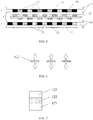
FIG. 1 is a sectional structural diagram of a double-faced display panel according to a first embodiment of the invention; -
FIG. 2 is a light emitting schematic diagram of a sub pixel inFIG. 1 ; -
FIG. 3 is a structural schematic diagram of the sub pixel inFIG. 1 ; -
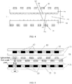
FIG. 4 is a schematic sectional diagram of a reflection unit according to the first embodiment of the invention; -
FIG. 5 is a light path schematic diagram of the double-faced display panel under a light emitting state of the sub pixel inFIG. 1 ; and -
FIG. 6 is a light path schematic diagram of the double-faced display panel under a non-light emitting state of the sub pixel inFIG. 1 . - In order to make objects, technical details and advantages of the embodiments of the invention apparent, the technical solutions of the embodiment will be described in a clearly and fully understandable way in connection with the drawings related to the embodiments of the invention. It is obvious that the described embodiments are just a part but not all of the embodiments of the invention. Based on the described embodiments herein, those skilled in the art can obtain other embodiment(s), without any inventive work, which should be within the scope of the invention.
- The first embodiment of the invention provides a double-faced display panel; as shown in
FIG. 1 , the double-faced display panel comprises: afirst display sub-unit 1, provided with a first display surface and a first non-display surface opposite to each other; asecond display sub-unit 2, provided with a second display surface and a second non-display surface opposite to each other, thesecond display sub-unit 2 being arranged back to back with thefirst display sub-unit 1, and the second non-display surface facing the first non-display surface; and areflection unit 3, arranged between thefirst display sub-unit 1 and thesecond display sub-unit 2, and configured to reflect display light emitted from thefirst display sub-unit 1 back to thefirst display sub-unit 1 and reflect display light emitted from thesecond display sub-unit 2 back to thesecond display sub-unit 2. - Exemplarily, as shown in
FIG. 1 , thefirst display sub-unit 1 includes twofirst substrates 11 oppositely arranged and a plurality offirst sub-pixels 12 arranged between the twofirst substrates 11; thesecond display sub-unit 2 includes twosecond substrates 21 oppositely arranged and a plurality ofsecond sub-pixels 22 arranged between the twosecond substrates 21. In this way, light emitted from thefirst display sub-unit 1 is emitted by thefirst sub-pixels 12 of thefirst display sub-unit 1, light emitted from thesecond display sub-unit 2 is emitted by thesecond sub-pixels 22 of thefirst display sub-unit 1, and thereflection unit 3 is configured to reflect the light emitted from thefirst sub-pixels 12 back to thefirst display sub-unit 1 and reflect the light emitted fromsecond sub-pixels 22 back to thesecond display sub-unit 2. - Exemplarily, each of the
first sub-pixels 12 and thesecond sub-pixels 22 includes an Organic Light-Emitting Diode (OLED), wherein the OLED may be of a top emitting type or a double directional emitting type. For example, when the OLED included by each of thefirst sub-pixels 12 and thesecond sub-pixels 22 is of the top emitting type, namely, each OLED of thefirst sub-pixels 12 and each OLED of thesecond sub-pixels 22 respectively emit light to the display surfaces disposed back to back of the first display sub-unit and the second display sub-unit, as thereflection unit 3 is arranged between the non-display surfaces facing each other of the first display sub-unit and the second display sub-unit, thereflection unit 3 can reflect the light deflected and emitted to the non-display surfaces back to the first display sub-unit and the second display sub-unit, thus improving the light utilization. For example, as shown in a light emitting schematic diagram of each sub-pixel inFIG. 2 , when the OLED included by each of thefirst sub-pixels 12 and thesecond sub-pixels 22 is the double directional emitting type, one OLED can not only emit light to the top, but also emit light to the bottom (i.e., a side facing the reflection unit 3), the light emitted to the top can directly be transmitted through thefirst display sub-unit 1 or thesecond display sub-unit 2 for use, and the light emitted to the bottom is reflected by thereflection unit 3 and then be transmitted through thefirst display sub-unit 1 or thesecond display sub-unit 2 for use, thus improving the light utilization of the double-faced display panel. - Exemplarily, a structure of each OLED included by each of the
first sub-pixels 12 and thesecond sub-pixels 22 may include three layers: an anode, a light emitting layer and a cathode, for example,FIG. 3 shows the structure of the OLED included by thefirst sub-pixel 12, comprising: ananode 121, acathode 123 and alight emitting layer 122 arranged between theanode 121 and thecathode 123. Of course, in order to further improve performance of the OLED, the OLED may further include an organic functional layer arranged between theanode 121 and thecathode 123, and the organic functional layer includes at least one of a hole injection layer, a hole transport layer, an electron blocking layer, a hole and exciton blocking layer, an electron transport layer and an electron injection layer. The organic functional layer may be flexibly selected according to needs in actual application, which will not be repeated herein. - In addition, it should be noted that for the OLED of top emitting type, an electrode arranged close to the display surface of the first or second display sub-unit may be an anode or a cathode, but is a transparent electrode, correspondingly, the other electrode except the electrode close to the display surface may be a non-transparent electrode or a reflection electrode; for the OLED of double directional emitting type, at least one of the cathode or the anode is transparent.
- Exemplarily, the
first sub-pixels 21 may include first sub-pixels with three colors of red (R), green (G) and blue (B), and thesecond sub-pixels 22 may also include second sub pixels with three colors of red (R), green (G) and blue (B), that is to say, color display is realized in a full color manner. Or, each of the first sub-pixels and the second sub-pixels may include a white OLED, and RGB color filters are arranged on the substrates at a light exitting side, so the full color display is realized in a WOLED-COA manner; of course, the color display may be realized in a WOLED-CF (a white OLED and four color filters of R, G, B, W) manner, which is not limited by the embodiment of the invention. - Exemplarily, the
reflection unit 3 includes aswitch layer 33 and afirst reflection layer 31 and asecond reflection layer 32 which are respectively complementarily arranged on both sides of theswitch layer 33 in a staggered manner. Thefirst reflection layer 31 and thesecond reflection layer 32 may be a reflection mirror, for example, a chemically silvered silver mirror. Thefirst reflection layer 31 is disposed to correspond to thefirst sub-pixels 12 and is separated from thefirst display sub-unit 1 by thesecond reflection layer 32 and theswitch layer 33, thesecond reflection layer 32 is disposed to correspond to thesecond sub-pixels 22 and is separated from thesecond display sub-unit 2 by thefirst reflection layer 31 and theswitch layer 33, thefirst reflection layer 31 is arranged on a side of theswitch layer 33 close to thesecond display sub-unit 2, and thesecond reflection layer 32 is arranged on a side of theswitch layer 33 close to thefirst display sub-unit 1. In the embodiment, thefirst reflection layer 31 and thesecond reflection layer 32 are arranged on both sides of theswitch layer 33, "staggered" means that orthogonal projections of thefirst reflection layer 31 and thesecond reflection layer 32 do not overlap on theswitch layer 33, and "complementarily" means that thefirst reflection layer 31 and thesecond reflection layer 32 can form a whole seamless pattern by parallel movement to the same plane. - The
switch layer 33 is mainly used for adjusting light to activate or deactivate reflection. Exemplarily, as shown inFIG. 4 , theswitch layer 33 includes a liquid crystal cell, the liquid crystal cell including anupper substrate 331, alower substrate 333 and aliquid crystal layer 332 arranged between theupper substrate 331 and thelower substrate 333, wherein the liquid crystal cell further includes a control electrode, the control electrode including: a plurality of firstupper electrodes 311 and secondupper electrodes 321 which are alternately arranged at an interval on a side of theupper substrate 331 close to theliquid crystal layer 332, and a plurality of firstlower electrodes 312 and secondlower electrodes 322 which are alternately arranged at an interval on a side of thelower substrate 333 close to theliquid crystal layer 332, wherein the firstupper electrodes 311 and the firstlower electrodes 312 are arranged in pair and correspond to thefirst reflection layer 31, the secondupper electrodes 321 and the secondlower electrodes 322 are arranged in pair and correspond to thesecond reflection layer 32, the firstupper electrodes 311 and the firstlower electrodes 312 cooperate with each other to control corresponding liquid crystal in the liquid crystal cell to deflect, and the secondupper electrodes 321 and the secondlower electrodes 322 cooperate with each other to control corresponding liquid crystal in the liquid crystal cell to deflect. - Exemplarily, when the first
upper electrodes 311 and the firstlower electrodes 312 are respectively applied with voltages with a voltage difference, the liquid crystal positioned between the firstupper electrodes 311 and the firstlower electrodes 312 in the liquid crystal cell deflects, and when the secondupper electrodes 321 and the secondlower electrodes 322 are respectively applied with voltages with a voltage difference, the liquid crystal positioned between the secondupper electrodes 321 and the secondlower electrodes 322 in the liquid crystal cell deflects. Herein, the plurality of firstupper electrodes 311 may be applied with a same voltage, the plurality of firstlower electrodes 312 may be applied with a same voltage, the plurality of secondupper electrodes 321 may be applied with a same voltage, the plurality of secondlower electrodes 322 may be applied with a same voltage, the first upper electrodes and the second upper electrodes are respectively controlled, and the first lower electrodes and the second lower electrodes are respectively controlled. For example, the firstupper electrodes 311 and the firstlower electrodes 312 are respectively applied with a positive voltage and a reference voltage, and the secondupper electrodes 321 and the secondlower electrodes 322 are respectively applied with a positive voltage and a reference voltage, and in this way, an electric field is formed by applying a voltage to the control electrode, so that deflection of the liquid crystal can be conveniently controlled. - Exemplarily, the control electrode may be made from transparent electrode material, for example, Indium Tin Oxide (ITO), and the liquid crystal in the liquid crystal cell sandwiched between two layers of sub-electrodes may be Twisted Nematic (TN) type liquid crystal; namely, the liquid crystal deflects to form a transparent state when an electric field is applied, and is in an non-transparent state when no electric field is applied. A light control state of the
reflection unit 3 is changed by controlling a magnitude of the electric field between the sub-electrodes. - In the embodiment, the
switch layer 33 may be switched between two different optical states of the transparent state and the non-transparent state, so the reflection layer performs a function or not. Exemplarily, as shown inFIG. 5 , when a certain sub-pixel is in a light (light emitting) state, the control electrode in a corresponding region is controlled to apply an electric field, liquid crystal molecules are regularly arranged perpendicular to the electric field, and refractive indexes of the liquid crystal molecules are matched to form the transparent state, so the reflection layer corresponding to the sub-pixel play a role, and light emitted by the transparent sub-pixel can be reflected, so as to achieve a highlight display effect and an energy-saving aim; as shown inFIG. 6 , when a certain sub-pixel is in a dark (non-light emitting) state, no electric field is formed by controlling the control electrode in the corresponding region, the liquid crystal molecules are irregularly arranged; as the refractive indexes of the liquid crystal molecules are anisotropic, a non-transparent state is formed, incident ambient light is blocked by theswitch layer 33, the reflection layer corresponding to the sub-pixel does not play a role, and the ambient light cannot be reflected by the reflection layer, and the ambient light is absorbed when irradiating the double-faced display panel regardless of brightness of the ambient light, so as to achieve the aim of improving the contrast between the ambient light and the display brightness of the display panel. - In the double-faced display panel of the embodiment, the
first display sub-unit 1 further includes first black matrixes (BM) 13 arranged between adjacentfirst sub-pixels 12, thesecond display sub-unit 2 further includes secondblack matrixes 23 arranged between adjacentsecond sub-pixels 22, thefirst reflection layer 31 is disposed to correspond to the secondblack matrixes 23, and thesecond reflection layer 32 is disposed to correspond to the firstblack matrixes 13. - Exemplarily, the
first reflection layer 31, thefirst sub-pixel 12 and the secondblack matrix 23 are same in area; and thesecond reflection layer 32, thesecond sub-pixel 22 and the firstblack matrix 13 are same in area. Namely, the sub-pixels in thefirst display sub-unit 1 and thesecond display sub-unit 2 are arranged in a staggering manner respectively, thefirst sub-pixels 12 of thefirst display sub-unit 1 correspond to thefirst reflection layer 31 and the secondblack matrixes 23 of thesecond display sub-unit 2, which not only effectively use light emitted by thefirst sub-pixels 12 in thefirst display sub-unit 1 to improve light utilization of thefirst display sub-unit 1, but also does not influence operation of thesecond display sub-unit 2; similarly, thesecond sub-pixels 22 of thesecond display sub-unit 2 correspond to thesecond reflection layer 32 and the firstblack matrixes 13 of thefirst display sub-unit 1, which not only effectively use light emitted by thesecond sub-pixels 22 in thesecond display sub-unit 2 to improve light utilization of thesecond display sub-unit 2, but also does not influence operation of thefirst display sub-unit 1. - Of course, the areas of the
first reflection layer 31, thefirst sub-pixel 12 and the secondblack matrix 23 may also be different, and the areas of thesecond reflection layer 32, thesecond sub-pixel 22 and the firstblack matrix 13 may also be different, as long as the operation of thesecond display sub-unit 2 and that of thefirst display sub-unit 1 do not affect each other and the light utilization can be improved, which is not limited by the embodiment of the invention. - Exemplarily, the
first sub-pixel 12 and thesecond sub-pixel 22 are same in area. In this way, the areas of thefirst sub-pixel 12, the firstblack matrix 13 and thefirst reflection layer 31 in thefirst display sub-unit 1 are same as those of thesecond sub-pixel 22, the secondblack matrix 23 and thesecond reflection layer 32 in thesecond display sub-unit 2, in order to further simplify a design process and improve process efficiency. - Further, an embodiment of the invention further provides a manufacturing method of a double-faced display panel; when the above double-faced display panel is manufactured, the
first display sub-unit 1, thesecond display sub-unit 2 and thereflection unit 3 may be manufactured respectively, then they are bonded with a sealant to form a whole; also one display sub-unit may be taken as a reference, and thereflection unit 3 and the other display sub-unit may be formed on one side of the display sub-unit in sequence. - Hereinafter, by taking an example of forming the double-faced display panel in the second manner, the process is simply described as follows:
- Step 1: manufacturing a sub-pixel including an OLED and a black matrix on a first base substrate, for example, a transparent substrate, and arranging a second base substrate opposite to the first base substrate, to form one display sub-unit.
- Exemplarily, each sub-pixel may emit red (R), green (G) or blue (B) color light, and the black matrix and the sub pixel are same in area.
- Step 2: manufacturing a reflection layer at a position, corresponding to the black matrix, of the second base substrate at a non-display surface of the display sub-unit; and then forming a switch layer and the other switch layer on the reflection layer, wherein the positions of the two reflection layers are staggered and complementary;
- Step 3: arranging a third base substrate, for example a transparent substrate, on the other reflection layer, and then manufacturing a sub-pixel including an OLED and a black matrix on the third base substrate and arranging a fourth base substrate opposite to the third base substrate, to form the other display sub-unit.
In the double-faced display panel in the embodiment, as the reflection unit is arranged between the two display sub-units arranged back to back, the reflection unit can reflect displaying light emitted by each of the display sub-units and travelling to the non-display surface back to the corresponding display sub-unit for reuse, and can block ambient light, so that the double-faced display panel has higher display brightness and high contrast, the contrast between the display brightness of the display panel and the ambient light can be improved, a better display effect is achieved, and in addition, more energy is saved under the condition of the same display brightness. - The second embodiment of the invention provides a double-faced display device, comprising a display panel and a drive circuit connected with the display panel, and the display panel is the double-faced display panel in the first embodiment. Wherein, the first display sub-unit and the second display sub-unit have independent drive circuits, and the first display sub-unit and the second display sub-unit display same or different images at a certain moment.
- In the double-faced display device of the embodiment, one assembly manner is: firstly bonding two
first substrates 11 with afirst sub-pixel 12 by a sealant to form afirst display sub-unit 1; meanwhile, connecting twosecond substrates 21 with asecond sub-pixel 22 by a sealant to form asecond display sub-unit 2; then arranging areflection unit 3 between thefirst display sub-unit 1 and thesecond display sub-unit 2, aligning them, and performing frame sealing by using a sealant, so as to obtain the double-faced display device. - The double-faced display device has two independent input ports, through which same or different signals may be input; and correspondingly, same or different image information may be displayed.
- When the two display sub-units of the double-faced display device display a same image, same signal sources are input to a drive port corresponding to the
first display sub-unit 1 and a drive port corresponding to thesecond display sub-unit 2, and the same image information is sent to thefirst display sub-unit 1 and thesecond display sub-unit 2 for display at the same time; such a driving manner is usually used for a square panel, a highway billboards or other occasions where double-faced display is needed. - When the two display sub-units of the double-faced display device display different images, different signal sources are input to the drive port corresponding to the
first display sub-unit 1 and the drive port corresponding to thesecond display sub-unit 2, and different image information are respectively sent to thefirst display sub-unit 1 and thesecond display sub-unit 2 for display; such a driving manner is usually used for a medical instrument, a teaching equipment, or double-faced panels and other occasions where double-faced display is needed. - In the double-faced display device, as the double-faced display panel thereof adopts the reflection unit to reflect the light emitted from the sub-pixels in the first display sub-unit and the second display sub-unit and travelling to the non-display surface for reuse, the light utilization of the double-faced display device is improved, and highlight and better contrast are realized, so the display device has better display effect, and a viewer can easily recognize a picture even under bright light and obtain a better visual experience.
- It should be understood that the foregoing embodiments are only exemplary embodiments of the invention to describe the principle of the invention; however, the invention is not limited thereto. Those ordinarily skilled in the art can make various changes and modifications without departing from the spirit and essence of the invention, and such changes and modifications also fall into the protection scope of the invention.
- The application claims priority of Chinese Patent Application No.
201410332533.X filed on July 11, 2014
Claims (16)
- A double-faced display panel, comprising:a first display sub-unit, provided with a first display surface and a first non-display surface opposite to each other;a second display sub-unit, provided with a second display surface and a second non-display surface opposite to each other, and arranged back to back with the first display sub-unit, the second non-display surface facing the first non-display surface; anda reflection unit, arranged between the first display sub-unit and the second display sub-unit,wherein the reflection unit is configured to reflect displaying light emitted from the first display sub-unit back to the first display sub-unit and reflect displaying light emitted from the second display sub-unit back to the second display sub-unit.
- The double-faced display panel according to claim 1, wherein the reflection unit comprises a switch layer, and a first reflection layer and a second reflection layer which are respectively complementarily arranged on both sides of the switch layer in a staggered manner, the first reflection layer is arranged on a side of the switch layer close to the second display sub-unit, and the second reflection layer is arranged on a side of the switch layer close to the first display sub-unit.
- The double-faced display panel according to claim 2, wherein the first display sub-unit comprises two first substrates oppositely arranged and a plurality of first sub-pixels arranged between the two first substrates, and the second display sub-unit comprises two second substrates oppositely arranged and a plurality of second sub-pixels arranged between the two second substrates.
- The double-faced display panel according to claim 3, wherein the first reflection layer is disposed to correspond to the first sub-pixels and the second reflection layer is disposed to correspond to the second sub-pixels.
- The double-faced display panel according to claim 4, wherein a first black matrix is arranged between any two adjacent of the plurality of first sub-pixels, and a second black matrix is arranged between any two adjacent of the plurality of second sub-pixels.
- The double-faced display panel according to any one of claims 2 to 4, wherein the switch layer comprises: an upper substrate, a lower substrate, a liquid crystal layer arranged between the upper substrate and the lower substrate, and a control electrode arranged on sides of the upper substrate and the lower substrate close to the liquid crystal layer, the control electrode being applied with a voltage to control liquid crystal in a liquid crystal cell to deflect.
- The double-faced display panel according to claim 6, wherein the control electrode comprises a plurality of first upper electrodes and a plurality of second upper electrodes which are alternately arranged at an interval on a side of the upper substrate close to the liquid crystal layer, and a plurality of first lower electrodes and a plurality of second lower electrodes which are alternately arranged at an interval on a side of the lower substrate close to the liquid crystal layer.
- The double-faced display panel according to claim 7, wherein the first upper electrodes and the second upper electrodes are respectively applied with a positive voltage and a reference voltage, and the first lower electrodes and the second lower electrodes are respectively applied with a positive voltage and a reference voltage.
- The double-faced display panel according to claim 5, wherein the first reflection layer is disposed opposite to the second black matrix and the second reflection layer is disposed opposite to the first black matrix.
- The double-faced display panel according to claim 9, wherein the first reflection layer, the first sub-pixel and the second black matrix are same in area; and the second reflection layer, the second sub-pixel and the first black matrix are same in area.
- The double-faced display panel according to claim 10, wherein the first sub-pixel and the second sub-pixel are same in area.
- The double-faced display panel according to any one of claims 3 to 11, wherein each of the plurality of first sub-pixels and the plurality of second sub-pixels comprises an organic light-emitting member.
- The double-faced display panel according to claim 12, wherein the organic light-emitting member is of a double directional emitting type or a top emitting type.
- The double-faced display panel according to claim 3, wherein the plurality of first sub-pixels comprise red, green and blue sub-pixels and the plurality of second sub-pixels comprise red, green and blue sub-pixels.
- A double-faced display device, comprising:a display panel, being the double-faced display panel according to any one of claims 1 to 14; anda drive circuit connected with the display panel.
- The double-faced display device according to claim 15, wherein the first display sub-unit and the second display sub-unit respectively have independent drive circuits, and the first display sub-unit and the second display sub-unit display same or different images at a certain moment.
Applications Claiming Priority (2)
| Application Number | Priority Date | Filing Date | Title |
|---|---|---|---|
| CN201410332533.XA CN104155791B (en) | 2014-07-11 | 2014-07-11 | Double-sided display panel and double-sided display device |
| PCT/CN2014/092957 WO2016004726A1 (en) | 2014-07-11 | 2014-12-03 | Double-surface display panel and double-surface display apparatus |
Publications (3)
| Publication Number | Publication Date |
|---|---|
| EP3168677A1 true EP3168677A1 (en) | 2017-05-17 |
| EP3168677A4 EP3168677A4 (en) | 2018-04-18 |
| EP3168677B1 EP3168677B1 (en) | 2019-07-31 |
Family
ID=51881330
Family Applications (1)
| Application Number | Title | Priority Date | Filing Date |
|---|---|---|---|
| EP14882144.0A Not-in-force EP3168677B1 (en) | 2014-07-11 | 2014-12-03 | Double-surface display panel and double-surface display apparatus |
Country Status (4)
| Country | Link |
|---|---|
| US (1) | US9997583B2 (en) |
| EP (1) | EP3168677B1 (en) |
| CN (1) | CN104155791B (en) |
| WO (1) | WO2016004726A1 (en) |
Cited By (1)
| Publication number | Priority date | Publication date | Assignee | Title |
|---|---|---|---|---|
| CN109768063A (en) * | 2019-01-28 | 2019-05-17 | 京东方科技集团股份有限公司 | A kind of two-sided display screen and display device |
Families Citing this family (40)
| Publication number | Priority date | Publication date | Assignee | Title |
|---|---|---|---|---|
| KR101511117B1 (en) * | 2014-01-07 | 2015-04-10 | 주식회사 토비스 | A Dual-sided Display |
| CN104155791B (en) * | 2014-07-11 | 2017-01-18 | 京东方科技集团股份有限公司 | Double-sided display panel and double-sided display device |
| CN104391407B (en) * | 2014-12-15 | 2017-04-05 | 京东方科技集团股份有限公司 | The display packing of display device and display device |
| KR102380158B1 (en) * | 2015-04-24 | 2022-03-29 | 삼성디스플레이 주식회사 | Display device and manufacturing method thereof |
| CN105242443A (en) * | 2015-10-28 | 2016-01-13 | 深圳市华星光电技术有限公司 | Reflective dual-face LCD |
| US11243735B2 (en) | 2016-02-09 | 2022-02-08 | Lim Industries LLC | Electronic panel having multiple display devices and a multi-state device operable with a processor to control a see-through mode and a plurality of display modes |
| CN105810714B (en) | 2016-03-16 | 2019-03-15 | 武汉华星光电技术有限公司 | OLED display device with double-sided display and manufacturing method thereof |
| CN105785685B (en) | 2016-05-11 | 2018-03-09 | 深圳市华星光电技术有限公司 | Display with double faces, display module and its tft array substrate |
| KR102604993B1 (en) * | 2016-05-17 | 2023-11-27 | 삼성디스플레이 주식회사 | Organic light emitting display apparatus |
| US10339531B2 (en) | 2016-06-10 | 2019-07-02 | Bank Of America Corporation | Organic light emitting diode (“OLED”) security authentication system |
| US10970027B2 (en) | 2016-06-21 | 2021-04-06 | Bank Of America Corporation | Combination organic light emitting diode (“OLED”) device |
| US10783336B2 (en) | 2016-06-21 | 2020-09-22 | Bank Of America Corporation | Reshape-able OLED device for positioning payment instrument |
| US10163154B2 (en) * | 2016-06-21 | 2018-12-25 | Bank Of America Corporation | OLED (“organic light emitting diode”) teller windows |
| US9665818B1 (en) | 2016-06-21 | 2017-05-30 | Bank Of America Corporation | Organic light emitting diode (“OLED”) universal plastic |
| US10460135B1 (en) | 2016-06-21 | 2019-10-29 | Bank Of America Corporation | Foldable organic light emitting diode (“OLED”) purchasing instrument reader |
| US10001640B1 (en) * | 2016-06-27 | 2018-06-19 | Amazon Technologies, Inc. | Relocating common connector pads in display devices |
| US10580068B2 (en) | 2016-07-11 | 2020-03-03 | Bank Of America Corporation | OLED-based secure monitoring of valuables |
| US10043183B2 (en) | 2016-08-30 | 2018-08-07 | Bank Of America Corporation | Organic light emitting diode (“OLED”) visual authentication circuit board |
| US10176676B2 (en) | 2016-09-23 | 2019-01-08 | Bank Of America Corporation | Organic light emitting diode (“OLED”) display with quick service terminal (“QST”) functionality |
| US10156714B1 (en) * | 2017-03-22 | 2018-12-18 | Amazon Technologies, Inc. | Electrowetting pixel with bottom electrode to reduce electromagnetic fringe fields |
| CN107274786B (en) * | 2017-07-06 | 2021-04-06 | 京东方科技集团股份有限公司 | Display panel, display device and display method |
| CN107255888A (en) * | 2017-08-03 | 2017-10-17 | 深圳市华星光电技术有限公司 | Double face display panel and display device |
| KR102502881B1 (en) | 2018-01-16 | 2023-02-24 | 엘지전자 주식회사 | Display device |
| CN108459442A (en) * | 2018-02-11 | 2018-08-28 | 深圳市华星光电技术有限公司 | Double-side display device |
| CN108400155B (en) | 2018-04-23 | 2020-06-05 | 京东方科技集团股份有限公司 | OLED double-sided display panel and preparation method thereof |
| CN109192763A (en) * | 2018-09-11 | 2019-01-11 | 武汉华星光电半导体显示技术有限公司 | OLED display |
| US10916731B2 (en) | 2018-09-11 | 2021-02-09 | Wuhan China Star Optoelectronics Semiconductor Display Technology Co., Ltd. | Organic light emitting diode display device |
| CN109300968B (en) * | 2018-11-22 | 2022-05-20 | 合肥鑫晟光电科技有限公司 | Display substrate, display device and display control method |
| CN109273518A (en) | 2018-11-26 | 2019-01-25 | 京东方科技集团股份有限公司 | Display substrate, manufacturing method thereof, display device and control method thereof |
| CN109559536B (en) * | 2018-12-10 | 2021-06-08 | 百度在线网络技术(北京)有限公司 | Traffic light, traffic light identification method, traffic light identification device, traffic light identification equipment and storage medium |
| WO2020205712A1 (en) * | 2019-04-04 | 2020-10-08 | Lim Industries LLC | Electronic panel having multiple display devices operable with a multi-state device |
| US11138488B2 (en) | 2019-06-26 | 2021-10-05 | Bank Of America Corporation | Organic light emitting diode (“OLED”) single-use payment instrument |
| CN112782893B (en) * | 2019-11-08 | 2022-08-26 | 京东方科技集团股份有限公司 | Display panel, driving method and preparation method thereof, and display device |
| KR102835329B1 (en) * | 2019-12-05 | 2025-07-16 | 엘지디스플레이 주식회사 | Display Device And Method Of Fabricating The Same |
| US11164822B1 (en) * | 2020-09-28 | 2021-11-02 | United Microelectronics Corp. | Structure of semiconductor device and method for bonding two substrates |
| CN113053966B (en) | 2021-03-09 | 2023-08-22 | 京东方科技集团股份有限公司 | Display panel, brightness compensation method and display device |
| CN113299708B (en) * | 2021-05-12 | 2022-09-09 | 武汉华星光电技术有限公司 | Double-sided display panel and preparation method thereof |
| CN113238415B (en) * | 2021-05-13 | 2023-05-23 | 北京京东方技术开发有限公司 | Transparent display panel and display device |
| CN116096167A (en) * | 2023-01-20 | 2023-05-09 | 京东方科技集团股份有限公司 | Double-sided display panel and double-sided display device |
| CN118519295B (en) * | 2024-06-06 | 2026-04-21 | 昆山龙腾光电股份有限公司 | Dual-sided display device and driving method |
Family Cites Families (19)
| Publication number | Priority date | Publication date | Assignee | Title |
|---|---|---|---|---|
| JP2003185994A (en) * | 2001-12-14 | 2003-07-03 | Nanox Corp | Liquid crystal display |
| JP2004014316A (en) * | 2002-06-07 | 2004-01-15 | Rohm Co Ltd | Double-sided organic electroluminescent display module and information terminal |
| JP4159817B2 (en) | 2002-07-11 | 2008-10-01 | シチズンホールディングス株式会社 | Liquid crystal display |
| JP2004199028A (en) | 2002-10-24 | 2004-07-15 | Seiko Epson Corp | Display device and electronic equipment |
| US8681140B2 (en) * | 2004-05-21 | 2014-03-25 | Semiconductor Energy Laboratory Co., Ltd. | Display device and electronic apparatus having the same |
| TWI351549B (en) * | 2004-09-03 | 2011-11-01 | Hon Hai Prec Ind Co Ltd | Backlight module capable of emitting light from tw |
| US7259815B2 (en) * | 2004-10-28 | 2007-08-21 | Motorola Inc. | Two-way trans-reflective display |
| WO2007040028A1 (en) * | 2005-10-04 | 2007-04-12 | Sharp Kabushiki Kaisha | Liquid crystal display unit and portable electronic apparatus provided with it |
| CN2862090Y (en) * | 2005-10-12 | 2007-01-24 | 群康科技(深圳)有限公司 | Two-side display LCD |
| US7514861B2 (en) * | 2005-11-24 | 2009-04-07 | Chunghwa Picture Tubes, Ltd. | Organic electro-luminescent device |
| US8472101B2 (en) * | 2009-06-08 | 2013-06-25 | Industrial Technology Research Institute | Dual display |
| CN202736926U (en) * | 2012-08-29 | 2013-02-13 | 温兆楠 | Oled display |
| CN102998845B (en) * | 2012-12-11 | 2015-07-15 | 京东方科技集团股份有限公司 | Liquid crystal display (LCD) and display device |
| CN103257474B (en) * | 2013-03-15 | 2015-12-02 | 京东方科技集团股份有限公司 | A kind of double face display panel and double-side display device |
| CN103246105A (en) * | 2013-04-26 | 2013-08-14 | 京东方科技集团股份有限公司 | Liquid crystal display panel and liquid crystal display |
| CN203299494U (en) * | 2013-05-27 | 2013-11-20 | 北京京东方光电科技有限公司 | Double-face displayer |
| CN103293793B (en) * | 2013-05-31 | 2016-06-01 | 京东方科技集团股份有限公司 | A kind of double face display panel and manufacture method thereof |
| TW201504718A (en) * | 2013-07-16 | 2015-02-01 | Wintek Corp | Optoelectronic device |
| CN104155791B (en) * | 2014-07-11 | 2017-01-18 | 京东方科技集团股份有限公司 | Double-sided display panel and double-sided display device |
-
2014
- 2014-07-11 CN CN201410332533.XA patent/CN104155791B/en active Active
- 2014-12-03 EP EP14882144.0A patent/EP3168677B1/en not_active Not-in-force
- 2014-12-03 WO PCT/CN2014/092957 patent/WO2016004726A1/en not_active Ceased
- 2014-12-03 US US14/768,983 patent/US9997583B2/en active Active
Cited By (1)
| Publication number | Priority date | Publication date | Assignee | Title |
|---|---|---|---|---|
| CN109768063A (en) * | 2019-01-28 | 2019-05-17 | 京东方科技集团股份有限公司 | A kind of two-sided display screen and display device |
Also Published As
| Publication number | Publication date |
|---|---|
| CN104155791A (en) | 2014-11-19 |
| WO2016004726A1 (en) | 2016-01-14 |
| US9997583B2 (en) | 2018-06-12 |
| CN104155791B (en) | 2017-01-18 |
| EP3168677B1 (en) | 2019-07-31 |
| US20160254336A1 (en) | 2016-09-01 |
| EP3168677A4 (en) | 2018-04-18 |
Similar Documents
| Publication | Publication Date | Title |
|---|---|---|
| US9997583B2 (en) | Double-faced display panel and double-faced display device | |
| US10082903B2 (en) | Display panel and display device | |
| CN104898317B (en) | Dot structure and liquid crystal display panel | |
| EP3351998B1 (en) | 3d display apparatus and driving method therefor | |
| US10007107B2 (en) | Light valve and display device | |
| KR101948191B1 (en) | Electro wetting display apparatus | |
| US9429811B2 (en) | Display panel and display method thereof and display apparatus | |
| WO2018228047A1 (en) | Display device and method for driving same | |
| CN109920831A (en) | A kind of display panel and its driving method, display device | |
| JP2013041100A (en) | Transparent display device | |
| CN110412799B (en) | Display panel, driving method thereof and display device | |
| CN103323989B (en) | A kind of display | |
| CN117711338B (en) | Display module and display device | |
| CN105576005A (en) | Light-and-thin low-consumption 3D touch control type OLED display device | |
| CN105679232A (en) | Touch control-type 3D organic light emitting display (OLED) device | |
| CN103439832B (en) | Transparent display | |
| US20170309858A1 (en) | Display device | |
| CN109212832B (en) | Liquid crystal display panel and manufacturing method thereof, liquid crystal display device | |
| CN205644488U (en) | Three -dimensional organic electroluminescence display device of touch | |
| KR20070058149A (en) | Reflective color display device using cholesteric liquid crystal and its manufacturing method | |
| CN104793393A (en) | Display panel and display device | |
| CN117037731B (en) | Display panel and driving method, display device | |
| KR20070069721A (en) | Flexible display | |
| KR102607274B1 (en) | Liquid crystal transparent display | |
| US20170358635A1 (en) | Display device |
Legal Events
| Date | Code | Title | Description |
|---|---|---|---|
| STAA | Information on the status of an ep patent application or granted ep patent |
Free format text: STATUS: THE INTERNATIONAL PUBLICATION HAS BEEN MADE |
|
| PUAI | Public reference made under article 153(3) epc to a published international application that has entered the european phase |
Free format text: ORIGINAL CODE: 0009012 |
|
| STAA | Information on the status of an ep patent application or granted ep patent |
Free format text: STATUS: REQUEST FOR EXAMINATION WAS MADE |
|
| 17P | Request for examination filed |
Effective date: 20150819 |
|
| AK | Designated contracting states |
Kind code of ref document: A1 Designated state(s): AL AT BE BG CH CY CZ DE DK EE ES FI FR GB GR HR HU IE IS IT LI LT LU LV MC MK MT NL NO PL PT RO RS SE SI SK SM TR |
|
| AX | Request for extension of the european patent |
Extension state: BA ME |
|
| DAX | Request for extension of the european patent (deleted) | ||
| RIC1 | Information provided on ipc code assigned before grant |
Ipc: H01L 25/04 20140101ALN20180308BHEP Ipc: H01L 27/32 20060101AFI20180308BHEP Ipc: G02F 1/1335 20060101ALI20180308BHEP Ipc: H01L 51/52 20060101ALI20180308BHEP |
|
| A4 | Supplementary search report drawn up and despatched |
Effective date: 20180316 |
|
| REG | Reference to a national code |
Ref country code: DE Ref legal event code: R079 Ref document number: 602014051069 Country of ref document: DE Free format text: PREVIOUS MAIN CLASS: G02F0001133500 Ipc: H01L0027320000 |
|
| GRAP | Despatch of communication of intention to grant a patent |
Free format text: ORIGINAL CODE: EPIDOSNIGR1 |
|
| STAA | Information on the status of an ep patent application or granted ep patent |
Free format text: STATUS: GRANT OF PATENT IS INTENDED |
|
| RIC1 | Information provided on ipc code assigned before grant |
Ipc: H01L 51/52 20060101ALI20190131BHEP Ipc: H01L 25/04 20140101ALN20190131BHEP Ipc: G02F 1/1335 20060101ALI20190131BHEP Ipc: H01L 27/32 20060101AFI20190131BHEP |
|
| INTG | Intention to grant announced |
Effective date: 20190221 |
|
| GRAS | Grant fee paid |
Free format text: ORIGINAL CODE: EPIDOSNIGR3 |
|
| GRAA | (expected) grant |
Free format text: ORIGINAL CODE: 0009210 |
|
| STAA | Information on the status of an ep patent application or granted ep patent |
Free format text: STATUS: THE PATENT HAS BEEN GRANTED |
|
| AK | Designated contracting states |
Kind code of ref document: B1 Designated state(s): AL AT BE BG CH CY CZ DE DK EE ES FI FR GB GR HR HU IE IS IT LI LT LU LV MC MK MT NL NO PL PT RO RS SE SI SK SM TR |
|
| REG | Reference to a national code |
Ref country code: CH Ref legal event code: EP Ref country code: GB Ref legal event code: FG4D |
|
| REG | Reference to a national code |
Ref country code: DE Ref legal event code: R096 Ref document number: 602014051069 Country of ref document: DE |
|
| REG | Reference to a national code |
Ref country code: AT Ref legal event code: REF Ref document number: 1161842 Country of ref document: AT Kind code of ref document: T Effective date: 20190815 |
|
| REG | Reference to a national code |
Ref country code: IE Ref legal event code: FG4D |
|
| REG | Reference to a national code |
Ref country code: NL Ref legal event code: FP |
|
| REG | Reference to a national code |
Ref country code: LT Ref legal event code: MG4D |
|
| REG | Reference to a national code |
Ref country code: AT Ref legal event code: MK05 Ref document number: 1161842 Country of ref document: AT Kind code of ref document: T Effective date: 20190731 |
|
| PG25 | Lapsed in a contracting state [announced via postgrant information from national office to epo] |
Ref country code: PT Free format text: LAPSE BECAUSE OF FAILURE TO SUBMIT A TRANSLATION OF THE DESCRIPTION OR TO PAY THE FEE WITHIN THE PRESCRIBED TIME-LIMIT Effective date: 20191202 Ref country code: FI Free format text: LAPSE BECAUSE OF FAILURE TO SUBMIT A TRANSLATION OF THE DESCRIPTION OR TO PAY THE FEE WITHIN THE PRESCRIBED TIME-LIMIT Effective date: 20190731 Ref country code: SE Free format text: LAPSE BECAUSE OF FAILURE TO SUBMIT A TRANSLATION OF THE DESCRIPTION OR TO PAY THE FEE WITHIN THE PRESCRIBED TIME-LIMIT Effective date: 20190731 Ref country code: HR Free format text: LAPSE BECAUSE OF FAILURE TO SUBMIT A TRANSLATION OF THE DESCRIPTION OR TO PAY THE FEE WITHIN THE PRESCRIBED TIME-LIMIT Effective date: 20190731 Ref country code: LT Free format text: LAPSE BECAUSE OF FAILURE TO SUBMIT A TRANSLATION OF THE DESCRIPTION OR TO PAY THE FEE WITHIN THE PRESCRIBED TIME-LIMIT Effective date: 20190731 Ref country code: NO Free format text: LAPSE BECAUSE OF FAILURE TO SUBMIT A TRANSLATION OF THE DESCRIPTION OR TO PAY THE FEE WITHIN THE PRESCRIBED TIME-LIMIT Effective date: 20191031 Ref country code: AT Free format text: LAPSE BECAUSE OF FAILURE TO SUBMIT A TRANSLATION OF THE DESCRIPTION OR TO PAY THE FEE WITHIN THE PRESCRIBED TIME-LIMIT Effective date: 20190731 Ref country code: BG Free format text: LAPSE BECAUSE OF FAILURE TO SUBMIT A TRANSLATION OF THE DESCRIPTION OR TO PAY THE FEE WITHIN THE PRESCRIBED TIME-LIMIT Effective date: 20191031 |
|
| PG25 | Lapsed in a contracting state [announced via postgrant information from national office to epo] |
Ref country code: IS Free format text: LAPSE BECAUSE OF FAILURE TO SUBMIT A TRANSLATION OF THE DESCRIPTION OR TO PAY THE FEE WITHIN THE PRESCRIBED TIME-LIMIT Effective date: 20191130 Ref country code: GR Free format text: LAPSE BECAUSE OF FAILURE TO SUBMIT A TRANSLATION OF THE DESCRIPTION OR TO PAY THE FEE WITHIN THE PRESCRIBED TIME-LIMIT Effective date: 20191101 Ref country code: AL Free format text: LAPSE BECAUSE OF FAILURE TO SUBMIT A TRANSLATION OF THE DESCRIPTION OR TO PAY THE FEE WITHIN THE PRESCRIBED TIME-LIMIT Effective date: 20190731 Ref country code: LV Free format text: LAPSE BECAUSE OF FAILURE TO SUBMIT A TRANSLATION OF THE DESCRIPTION OR TO PAY THE FEE WITHIN THE PRESCRIBED TIME-LIMIT Effective date: 20190731 Ref country code: RS Free format text: LAPSE BECAUSE OF FAILURE TO SUBMIT A TRANSLATION OF THE DESCRIPTION OR TO PAY THE FEE WITHIN THE PRESCRIBED TIME-LIMIT Effective date: 20190731 Ref country code: ES Free format text: LAPSE BECAUSE OF FAILURE TO SUBMIT A TRANSLATION OF THE DESCRIPTION OR TO PAY THE FEE WITHIN THE PRESCRIBED TIME-LIMIT Effective date: 20190731 |
|
| PG25 | Lapsed in a contracting state [announced via postgrant information from national office to epo] |
Ref country code: TR Free format text: LAPSE BECAUSE OF FAILURE TO SUBMIT A TRANSLATION OF THE DESCRIPTION OR TO PAY THE FEE WITHIN THE PRESCRIBED TIME-LIMIT Effective date: 20190731 |
|
| PG25 | Lapsed in a contracting state [announced via postgrant information from national office to epo] |
Ref country code: RO Free format text: LAPSE BECAUSE OF FAILURE TO SUBMIT A TRANSLATION OF THE DESCRIPTION OR TO PAY THE FEE WITHIN THE PRESCRIBED TIME-LIMIT Effective date: 20190731 Ref country code: PL Free format text: LAPSE BECAUSE OF FAILURE TO SUBMIT A TRANSLATION OF THE DESCRIPTION OR TO PAY THE FEE WITHIN THE PRESCRIBED TIME-LIMIT Effective date: 20190731 Ref country code: EE Free format text: LAPSE BECAUSE OF FAILURE TO SUBMIT A TRANSLATION OF THE DESCRIPTION OR TO PAY THE FEE WITHIN THE PRESCRIBED TIME-LIMIT Effective date: 20190731 Ref country code: DK Free format text: LAPSE BECAUSE OF FAILURE TO SUBMIT A TRANSLATION OF THE DESCRIPTION OR TO PAY THE FEE WITHIN THE PRESCRIBED TIME-LIMIT Effective date: 20190731 Ref country code: IT Free format text: LAPSE BECAUSE OF FAILURE TO SUBMIT A TRANSLATION OF THE DESCRIPTION OR TO PAY THE FEE WITHIN THE PRESCRIBED TIME-LIMIT Effective date: 20190731 |
|
| PG25 | Lapsed in a contracting state [announced via postgrant information from national office to epo] |
Ref country code: CZ Free format text: LAPSE BECAUSE OF FAILURE TO SUBMIT A TRANSLATION OF THE DESCRIPTION OR TO PAY THE FEE WITHIN THE PRESCRIBED TIME-LIMIT Effective date: 20190731 Ref country code: SM Free format text: LAPSE BECAUSE OF FAILURE TO SUBMIT A TRANSLATION OF THE DESCRIPTION OR TO PAY THE FEE WITHIN THE PRESCRIBED TIME-LIMIT Effective date: 20190731 Ref country code: SK Free format text: LAPSE BECAUSE OF FAILURE TO SUBMIT A TRANSLATION OF THE DESCRIPTION OR TO PAY THE FEE WITHIN THE PRESCRIBED TIME-LIMIT Effective date: 20190731 Ref country code: IS Free format text: LAPSE BECAUSE OF FAILURE TO SUBMIT A TRANSLATION OF THE DESCRIPTION OR TO PAY THE FEE WITHIN THE PRESCRIBED TIME-LIMIT Effective date: 20200224 |
|
| REG | Reference to a national code |
Ref country code: DE Ref legal event code: R097 Ref document number: 602014051069 Country of ref document: DE |
|
| PLBE | No opposition filed within time limit |
Free format text: ORIGINAL CODE: 0009261 |
|
| STAA | Information on the status of an ep patent application or granted ep patent |
Free format text: STATUS: NO OPPOSITION FILED WITHIN TIME LIMIT |
|
| PG2D | Information on lapse in contracting state deleted |
Ref country code: IS |
|
| PG25 | Lapsed in a contracting state [announced via postgrant information from national office to epo] |
Ref country code: IS Free format text: LAPSE BECAUSE OF FAILURE TO SUBMIT A TRANSLATION OF THE DESCRIPTION OR TO PAY THE FEE WITHIN THE PRESCRIBED TIME-LIMIT Effective date: 20191030 |
|
| REG | Reference to a national code |
Ref country code: CH Ref legal event code: PL |
|
| 26N | No opposition filed |
Effective date: 20200603 |
|
| REG | Reference to a national code |
Ref country code: BE Ref legal event code: MM Effective date: 20191231 |
|
| PG25 | Lapsed in a contracting state [announced via postgrant information from national office to epo] |
Ref country code: MC Free format text: LAPSE BECAUSE OF FAILURE TO SUBMIT A TRANSLATION OF THE DESCRIPTION OR TO PAY THE FEE WITHIN THE PRESCRIBED TIME-LIMIT Effective date: 20190731 Ref country code: SI Free format text: LAPSE BECAUSE OF FAILURE TO SUBMIT A TRANSLATION OF THE DESCRIPTION OR TO PAY THE FEE WITHIN THE PRESCRIBED TIME-LIMIT Effective date: 20190731 |
|
| PG25 | Lapsed in a contracting state [announced via postgrant information from national office to epo] |
Ref country code: LU Free format text: LAPSE BECAUSE OF NON-PAYMENT OF DUE FEES Effective date: 20191203 Ref country code: IE Free format text: LAPSE BECAUSE OF NON-PAYMENT OF DUE FEES Effective date: 20191203 |
|
| PG25 | Lapsed in a contracting state [announced via postgrant information from national office to epo] |
Ref country code: CH Free format text: LAPSE BECAUSE OF NON-PAYMENT OF DUE FEES Effective date: 20191231 Ref country code: LI Free format text: LAPSE BECAUSE OF NON-PAYMENT OF DUE FEES Effective date: 20191231 Ref country code: BE Free format text: LAPSE BECAUSE OF NON-PAYMENT OF DUE FEES Effective date: 20191231 |
|
| PG25 | Lapsed in a contracting state [announced via postgrant information from national office to epo] |
Ref country code: CY Free format text: LAPSE BECAUSE OF FAILURE TO SUBMIT A TRANSLATION OF THE DESCRIPTION OR TO PAY THE FEE WITHIN THE PRESCRIBED TIME-LIMIT Effective date: 20190731 |
|
| PG25 | Lapsed in a contracting state [announced via postgrant information from national office to epo] |
Ref country code: HU Free format text: LAPSE BECAUSE OF FAILURE TO SUBMIT A TRANSLATION OF THE DESCRIPTION OR TO PAY THE FEE WITHIN THE PRESCRIBED TIME-LIMIT; INVALID AB INITIO Effective date: 20141203 Ref country code: MT Free format text: LAPSE BECAUSE OF FAILURE TO SUBMIT A TRANSLATION OF THE DESCRIPTION OR TO PAY THE FEE WITHIN THE PRESCRIBED TIME-LIMIT Effective date: 20190731 |
|
| PG25 | Lapsed in a contracting state [announced via postgrant information from national office to epo] |
Ref country code: MK Free format text: LAPSE BECAUSE OF FAILURE TO SUBMIT A TRANSLATION OF THE DESCRIPTION OR TO PAY THE FEE WITHIN THE PRESCRIBED TIME-LIMIT Effective date: 20190731 |
|
| REG | Reference to a national code |
Ref country code: DE Ref legal event code: R079 Ref document number: 602014051069 Country of ref document: DE Free format text: PREVIOUS MAIN CLASS: H01L0027320000 Ipc: H10K0059000000 |
|
| P01 | Opt-out of the competence of the unified patent court (upc) registered |
Effective date: 20230706 |
|
| PGFP | Annual fee paid to national office [announced via postgrant information from national office to epo] |
Ref country code: GB Payment date: 20231116 Year of fee payment: 10 |
|
| PGFP | Annual fee paid to national office [announced via postgrant information from national office to epo] |
Ref country code: NL Payment date: 20231219 Year of fee payment: 10 Ref country code: FR Payment date: 20231120 Year of fee payment: 10 Ref country code: DE Payment date: 20231214 Year of fee payment: 10 |
|
| REG | Reference to a national code |
Ref country code: DE Ref legal event code: R119 Ref document number: 602014051069 Country of ref document: DE |
|
| REG | Reference to a national code |
Ref country code: NL Ref legal event code: MM Effective date: 20250101 |
|
| GBPC | Gb: european patent ceased through non-payment of renewal fee |
Effective date: 20241203 |
|
| PG25 | Lapsed in a contracting state [announced via postgrant information from national office to epo] |
Ref country code: NL Free format text: LAPSE BECAUSE OF NON-PAYMENT OF DUE FEES Effective date: 20250101 |
|
| PG25 | Lapsed in a contracting state [announced via postgrant information from national office to epo] |
Ref country code: DE Free format text: LAPSE BECAUSE OF NON-PAYMENT OF DUE FEES Effective date: 20250701 |
|
| PG25 | Lapsed in a contracting state [announced via postgrant information from national office to epo] |
Ref country code: GB Free format text: LAPSE BECAUSE OF NON-PAYMENT OF DUE FEES Effective date: 20241203 |
|
| PG25 | Lapsed in a contracting state [announced via postgrant information from national office to epo] |
Ref country code: FR Free format text: LAPSE BECAUSE OF NON-PAYMENT OF DUE FEES Effective date: 20241231 |