EP3166126A1 - Charged particle beam system - Google Patents
Charged particle beam system Download PDFInfo
- Publication number
- EP3166126A1 EP3166126A1 EP16196946.4A EP16196946A EP3166126A1 EP 3166126 A1 EP3166126 A1 EP 3166126A1 EP 16196946 A EP16196946 A EP 16196946A EP 3166126 A1 EP3166126 A1 EP 3166126A1
- Authority
- EP
- European Patent Office
- Prior art keywords
- sample holder
- type
- eds
- charged particle
- sample
- Prior art date
- Legal status (The legal status is an assumption and is not a legal conclusion. Google has not performed a legal analysis and makes no representation as to the accuracy of the status listed.)
- Granted
Links
Images




Classifications
-
- H—ELECTRICITY
- H01—ELECTRIC ELEMENTS
- H01J—ELECTRIC DISCHARGE TUBES OR DISCHARGE LAMPS
- H01J37/00—Discharge tubes with provision for introducing objects or material to be exposed to the discharge, e.g. for the purpose of examination or processing thereof
- H01J37/02—Details
- H01J37/023—Means for mechanically adjusting components not otherwise provided for
-
- H—ELECTRICITY
- H01—ELECTRIC ELEMENTS
- H01J—ELECTRIC DISCHARGE TUBES OR DISCHARGE LAMPS
- H01J37/00—Discharge tubes with provision for introducing objects or material to be exposed to the discharge, e.g. for the purpose of examination or processing thereof
- H01J37/02—Details
- H01J37/04—Arrangements of electrodes and associated parts for generating or controlling the discharge, e.g. electron-optical arrangement or ion-optical arrangement
- H01J37/10—Lenses
-
- H—ELECTRICITY
- H01—ELECTRIC ELEMENTS
- H01J—ELECTRIC DISCHARGE TUBES OR DISCHARGE LAMPS
- H01J37/00—Discharge tubes with provision for introducing objects or material to be exposed to the discharge, e.g. for the purpose of examination or processing thereof
- H01J37/02—Details
- H01J37/20—Means for supporting or positioning the object or the material; Means for adjusting diaphragms or lenses associated with the support
-
- H—ELECTRICITY
- H01—ELECTRIC ELEMENTS
- H01J—ELECTRIC DISCHARGE TUBES OR DISCHARGE LAMPS
- H01J37/00—Discharge tubes with provision for introducing objects or material to be exposed to the discharge, e.g. for the purpose of examination or processing thereof
- H01J37/02—Details
- H01J37/244—Detectors; Associated components or circuits therefor
-
- H—ELECTRICITY
- H01—ELECTRIC ELEMENTS
- H01J—ELECTRIC DISCHARGE TUBES OR DISCHARGE LAMPS
- H01J37/00—Discharge tubes with provision for introducing objects or material to be exposed to the discharge, e.g. for the purpose of examination or processing thereof
- H01J37/26—Electron or ion microscopes; Electron or ion diffraction tubes
-
- G—PHYSICS
- G01—MEASURING; TESTING
- G01N—INVESTIGATING OR ANALYSING MATERIALS BY DETERMINING THEIR CHEMICAL OR PHYSICAL PROPERTIES
- G01N23/00—Investigating or analysing materials by the use of wave or particle radiation, e.g. X-rays or neutrons, not covered by groups G01N3/00 – G01N17/00, G01N21/00 or G01N22/00
- G01N23/20—Investigating or analysing materials by the use of wave or particle radiation, e.g. X-rays or neutrons, not covered by groups G01N3/00 – G01N17/00, G01N21/00 or G01N22/00 by using diffraction of the radiation by the materials, e.g. for investigating crystal structure; by using scattering of the radiation by the materials, e.g. for investigating non-crystalline materials; by using reflection of the radiation by the materials
- G01N23/20091—Measuring the energy-dispersion spectrum [EDS] of diffracted radiation
-
- H—ELECTRICITY
- H01—ELECTRIC ELEMENTS
- H01J—ELECTRIC DISCHARGE TUBES OR DISCHARGE LAMPS
- H01J2237/00—Discharge tubes exposing object to beam, e.g. for analysis treatment, etching, imaging
- H01J2237/02—Details
- H01J2237/024—Moving components not otherwise provided for
-
- H—ELECTRICITY
- H01—ELECTRIC ELEMENTS
- H01J—ELECTRIC DISCHARGE TUBES OR DISCHARGE LAMPS
- H01J2237/00—Discharge tubes exposing object to beam, e.g. for analysis treatment, etching, imaging
- H01J2237/244—Detection characterized by the detecting means
- H01J2237/2445—Photon detectors for X-rays, light, e.g. photomultipliers
-
- H—ELECTRICITY
- H01—ELECTRIC ELEMENTS
- H01J—ELECTRIC DISCHARGE TUBES OR DISCHARGE LAMPS
- H01J37/00—Discharge tubes with provision for introducing objects or material to be exposed to the discharge, e.g. for the purpose of examination or processing thereof
- H01J37/26—Electron or ion microscopes; Electron or ion diffraction tubes
- H01J37/28—Electron or ion microscopes; Electron or ion diffraction tubes with scanning beams
Definitions
- An analysis position at which the EDS detector 40 detects the characteristic X-rays emanating from the sample S is located within the sample chamber 15 and close to the sample S.
- the analysis position of the EDS detector 40 is determined by the EDS controller 52 based on information about the type of the sample holder 20 as described later.
- the EDS controller 52 determines the analysis position of the EDS detector 40 on the basis of both information about the type of the sample holder 20 and information about the type of the objective lens 16a.
Landscapes
- Chemical & Material Sciences (AREA)
- Analytical Chemistry (AREA)
- Analysing Materials By The Use Of Radiation (AREA)
Abstract
Description
- The present invention relates to a charged particle beam system.
- Electron microscopes, such as transmission electron microscope (TEM), scanning transmission electron microscope (STEM), and scanning electron microscopes (STEM), are used as means for obtaining structural information about nano-sized materials, devices, and biological samples. Where compositional information on such samples should be obtained, an energy dispersive X-ray spectrometer (EDS) detector is equipped to such an electron microscope.
- When EDS analysis is performed using an electron microscope equipped with an EDS detector, the EDS detector is inserted close to a sample placed within a sample chamber. When no EDS analysis is performed, the EDS detector is retracted from the sample chamber. By effecting such operations, where EDS analysis is not made, the electron microscope can be placed in a condition where neither observation of the sample nor exchange of the sample holder is hindered (see, for example, patent document 1).
- The insertion and retraction of the EDS detector are done under control of an EDS controller and are carried out, for example, when a user selects "IN" and "OUT", respectively, on the EDS detector via the manual control section of the EDS controller.
- Patent document 1:
JP-A-2011-153846 - In an electron microscope, an electron beam is directed at a sample, and an electron microscope image is formed by detecting secondary electrons or backscattered electrons emitted from the sample, electrons transmitted through the sample, or scattering electrons. When an electron beam is made to hit a sample, there are generated characteristic X-rays attributable to materials or elements constituting the sample. The produced characteristic X-rays have different energy bands for different elements. Therefore, compositional information about the sample can be obtained by detecting the characteristic X-rays.
- An EDS system including an EDS detector can detect characteristic X-rays and provide characteristic X-ray intensities which are different for different energy levels. The EDS system can perform various analyses such as point analysis, line analysis, and map analysis combined with scanned images.
- In recent years, silicon drift detectors (SDDs) have been put into practical use as EDS detectors and, therefore, higher sensitivity and higher speeds of EDS analysis are being accomplished. An SDD can have an improved detection efficiency by having a larger detector active area so as to increase the detection solid angle.
- The detection solid angle, Ω, is given by

- As can be seen from the above equation, in order to increase the detection solid angle of the EDS detector, the detector active area S must be increased, while the distance L must be reduced. Therefore, in order to increase the detection solid angle of the EDS detector, it is desirable to place the EDS detector as close as possible to the sample when the detector is inserted.
- However, if the EDS detector is placed closer to a sample, the EDS detector and sample holder may mechanically interfere with each other. Various types of sample holders are available. Different types of sample holders have different shapes and, therefore, it is difficult to place an EDS detector in an appropriate position for analysis.
- In view of the foregoing problem, the present invention has been made. One object associated with some aspects of the present invention is to provide a charged particle beam system in which a detector can be disposed in an appropriate analysis position.
- (1) A charged particle beam system associated with the present invention has: a charged particle source for producing charged particles; a sample holder for holding a sample; a detector for detecting, in an analysis position, a signal produced from the sample by impingement of the charged particles on the sample; a drive mechanism for moving the detector into the analysis position; and a controller for controlling the drive mechanism. The controller performs the steps of obtaining information about the type of the sample holder, determining the analysis position on the basis of the obtained information about the type of the sample holder, and controlling the drive mechanism to move the detector into the determined analysis position.
In this charged particle beam system, the controller performs the steps as described above and so the detector can be placed in an appropriate analysis position according to the type of the sample holder. Consequently, in this charged particle beam system, the detection solid angle can be increased by reducing the distance between the detector and the sample while preventing mechanical interference between the detector and the sample holder. Hence, in this charged particle beam system, the detection efficiency of the detector can be improved. - (2) In one feature of this charged particle beam system, the sample holder may be connected with the controller via plural signal lines. The controller may obtain information about the type of the sample holder on the basis of the state of electrical connection between the signal lines.
In this charged particle beam system, the type of the sample holder can be identified with a simple structure. - (3) In another feature of the charged particle beam system of (1), the sample holder may have an information storage section in which there is stored information about the type of the sample holder. The controller may obtain the information about the type of the sample holder by reading this information about the type of the sample holder from the information storage section.
- (4) In a further feature of the charged particle beam system of (1), there may be further included a manual control unit permitting a user to enter information about the type of the sample holder. The controller may obtain the information about the type of the sample holder on the basis of the information about the type of the sample holder entered via the manual control unit.
In this charged particle beam system, information about the type of the sample holder can be obtained without the need to interconnect the sample holder and the controller, for example, by a signal line such as a communication cable. - (5) In one feature of the charged particle beam system of any one of (1)-(4), there may be further included an objective lens. The controller may perform the step of obtaining information about the type of the objective lens. During the step of determining the analysis position, the controller may determine the analysis position on the basis of both the information about the type of the sample holder and the information about the type of the objective lens.
- In this charged particle beam system, the controller performs the steps as described above and so the detector can be disposed in an appropriate analysis position according both to the type of the sample holder and to the type of the objective lens. Therefore, in this charged particle beam system, the detection solid angle can be increased by reducing the distance between the detector and the sample while preventing both mechanical interference between the detector and the sample holder and the mechanical interference between the detector and the objective lens.
-
-
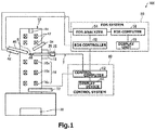
FIG. 1 is a schematic representation, partly in block form, of a charged particle beam system associated with a first embodiment of the present invention. -
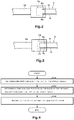
FIG. 2 is a schematic representation of a normal type sample holder identification portion. -
FIG. 3 is a schematic representation of a large solid angle compliant type sample holder identification portion. -
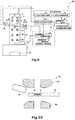
FIG. 4 is a flowchart illustrating one example of processing subroutine performed by an EDS controller of the system ofFIG. 1 . -
FIG. 5 illustrates an analysis position of an EDS detector of the system ofFIG. 1 assumed when the normal type sample holder has been inserted. -
FIG. 6 illustrates an analysis position of the EDS detector assumed when the large solid angle compliant type sample holder has been inserted. -
FIG. 7 is a schematic representation, partly in block form, of a charged particle beam system associated with a first modification of the first embodiment. -
FIG. 8 is a schematic representation, partly in block form, of a charged particle beam system associated with a second modification of the first embodiment. -
FIG. 9 is a schematic representation, partly in block form, of a charged particle beam system associated with a third modification of the first embodiment. -
FIG. 10 is a schematic representation of a sample chamber in the charged particle beam system ofFIG. 9 . -
FIG. 11 is a flowchart illustrating one example of processing subroutine performed by an EDS controller included in the charged particle beam system ofFIG. 9 . -
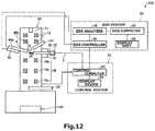
FIG. 12 is a schematic representation, partly in block form, of a charged particle beam system associated with a second embodiment. -
FIG. 13 illustrates an analysis position of an EDS detector of the system ofFIG. 12 assumed when the normal type sample holder has been inserted. -
FIG. 14 illustrates an analysis position of the EDS detector assumed when the large solid angle compliant type sample holder has been inserted. - The preferred embodiments of the present invention are hereinafter described in detail with reference to the drawings. It is to be understood that the embodiments described below are not intended to unduly restrict the content of the present invention delineated by the claims and that not all the configurations described below are essential constituent components of the invention.
- A charged particle beam system associated with a first embodiment of the present invention is first described by referring to
FIG. 1 , which schematically shows the charged particle beam system, generally indicated byreference numeral 100. - As shown in
FIG. 1 , the chargedparticle beam system 100 whose body portion is indicated bynumeral 10 includes asample holder 20, animage capture device 30, anSTEM detector 32, asecondary electron detector 34, anEDS detector 40, adrive mechanism 42, anEDS system 50, and acontrol system 60. - The
body portion 10 of the charged particle beam system includes an electron source 11 (which is one example of a charged particle source), anillumination lens system 12, asample stage 13, and animaging lens system 16. - The
electron source 11 produces electrons which are one kind of charged particles. For example, theelectron source 11 is an electron gun that emits an electron beam by accelerating electrons, emitted from a cathode, by means of an anode. - The electron beam generated by the
electron source 11 is focused onto a sample S by theillumination lens system 12 in asample chamber 15 such that the beam impinges on the sample S. - The charged
particle beam system 100 may be configured including deflectors (not shown) for causing the electron beam (electron probe) focused by theillumination lens system 12 to be scanned over the sample S. - The
sample stage 13 holds the sample S via thesample holder 20. Thesample stage 13 can move and stop the sample holder 20 (and the sample S). Thesample stage 13 can place the sample S in position. - The
sample chamber 15 is a space where the sample S is placed. In thesample chamber 15, electrons are made to impinge on the sample S. The interior of thesample chamber 15 is vacuum pumped by vacuum pumping equipment (not shown). - The
imaging lens system 16 forms an image from electrons transmitted through the sample S. Theimaging lens system 16 is made up of anobjective lens 16a, anintermediate lens 16b, and aprojector lens 16c. - The
sample holder 20 holds the sample S. Thesample stage 13 has a receptacle portion in which thesample holder 20 holding the sample S is inserted. Thus, the sample S is accommodated in thesample chamber 15.FIG. 1 shows a state in which thesample holder 20 has been inserted in thesample chamber 15. - The
sample holder 20 is connected to acontrol computer 62 and to anEDS controller 52 via communication cabling 2. In the illustrated example, thesample holder 20 is connected to theEDS controller 52 via both communication cabling 2 and controlcomputer 62. Alternatively, thesample holder 20 andEDS controller 52 may be interconnected by a communication cable without via thecontrol computer 62 in an unillustrated manner. - The communication cabling 2 is used for communications between the
sample holder 20 and theEDS controller 52 through thecontrol computer 62. The communication cabling 2 is ancillary to thesample holder 20, and connected to thecontrol computer 62 via a connector. The communication cabling 2 has a plurality of signal lines. - In the communication route between the
sample holder 20 and theEDS controller 52 via thecontrol computer 62, there may be A/D converters (not shown) or other circuits for converting signals output from thesample holder 20 into a form that is readable by thecontrol computer 62 andEDS controller 52. - The
sample holder 20 has atype identification portion 22 for identification of the type of thesample holder 20. Thetype identification portion 22 will be described in detail later. Thesample holder 20 may have a tilt stage for tilting the sample S, a rotary stage for rotating the sample S, a heater for controlling the temperature of the sample S, and other means. Control signals for controlling the tilting stage and other devices may be sent to thesample holder 20 from thecontrol computer 62 via the communication cabling 2. - The
image capture device 30 obtains a TEM (transmission electron microscope) image focused by theimaging lens system 16, for example, using a digital camera such as a CCD camera or CMOS camera. - The
STEM detector 32 detects the intensity of transmitted wave or diffracted wave passing through each point on the sample S by scanning the electron probe over the sample S. The output signal from theSTEM detector 32 is stored as STEM image data in a storage section (not shown) while being associated with information about the positions of electron impingement. - The
secondary electron detector 34 detects secondary electrons emitted from each point on the sample S in response to scanning of the electron probe over the sample S. The output signal from thesecondary electron detector 34 is stored as SE (secondary electron) image data into the storage section (not shown) while being associated with information about the positions of electron impingement. - The
EDS detector 40 detects characteristic X-rays (which are one example of signal produced from the sample by impingement of charged particles on the sample ) emanating from the sample S in response to impingement of electrons on the sample S. For example, theEDS detector 40 is a silicon drift detector. - An analysis position at which the
EDS detector 40 detects the characteristic X-rays emanating from the sample S is located within thesample chamber 15 and close to the sample S. The analysis position of theEDS detector 40 is determined by theEDS controller 52 based on information about the type of thesample holder 20 as described later. - The
drive mechanism 42 moves theEDS detector 40 into the analysis position. Thedrive mechanism 42 operates to insert thedetector 40 into the analysis position within thesample chamber 15 and to retract thedetector 40 from inside thesample chamber 15. - The
drive mechanism 42 is configured, for example, including a guide portion and a linear actuator for moving theEDS detector 40 on the guide portion on which theEDS detector 40 is slidably mounted. Position sensors are mounted on the guide portion to detect the position of theEDS detector 40. The plural position sensors are mounted in a corresponding manner to the plural analysis positions of theEDS detector 40. When theEDS detector 40 is located in the detection position of any one of the position sensors, this position sensor provides a detection signal. Note that no restriction is imposed on the configuration of thedrive mechanism 42 as long as it can insert and retract the detector. - The
EDS system 50 is used to perform EDS analysis. TheEDS system 50 has the above-described EDS controller 52 (that is one example of controller), anEDS analyzer 54, anEDS computer 56, and adisplay unit 58. - The
EDS controller 52 controls thedrive mechanism 42. The processing performed by theEDS controller 52 will be described later in "1.2. Operation of Charged Particle Beam System". The functions of theEDS controller 52 may be implemented by executing computer programs by means of a processor (such as a CPU or a DSP) or by using dedicated circuitry such as an ASIC (e.g., a gate array). - The
EDS analyzer 54 is a multichannel pulse height analyzer having multiple channels. TheEDS analyzer 54 counts the output signal from theEDS detector 40 for each X-ray energy range. - The
EDS computer 56 generates an EDS spectrum based on counts obtained by theEDS analyzer 54 for each X-ray energy range. - The
display unit 58 is an LCD, CRT, or the like. The EDS spectrum generated by theEDS computer 56 is displayed on thedisplay unit 58. - The
control system 60 controls thebody portion 10 of the charged particle beam system, as well as the components and devices making up the chargedparticle beam system 100 such as thesample holder 20. Thecontrol system 60 has thecontrol computer 62 and adisplay device 64. - The
control computer 62 performs processing to control thebody portion 10 of the charged particle beam, thesample holder 20, and other components. - The
display device 64 is an LCD, CRT, or the like. Information about various operating parameters such as the position of thesample holder 20, tilt angle, imaging mode (e.g., TEM mode, STEM mode, or SEM mode), and final magnification is displayed on thedisplay device 64. - As noted previously, the charged
particle beam system 100 functions as transmission electron microscope (TEM), scanning transmission electron microscope (STEM), and scanning electron microscope (STEM). Note that the chargedparticle beam system 100 may function as at least one of transmission electron microscope (TEM), scanning transmission electron microscope (STEM), and scanning electron microscope (STEM). - The
type identification portion 22 for identification of the type of thesample holder 20 is next described.FIG. 2 schematically shows atype identification portion 22a for a normaltype sample holder 20a that is one type of thesample holder 20.FIG. 3 schematically shows a type identification portion 22b for a large solid angle complianttype sample holder 20b that is another type of thesample holder 20. Each ofFIGS. 2 and 3 shows a state in which the communication cabling 2 is connected to thesample holder - The sample holder of the large solid angle compliant type referred to herein is designed to be capable of increasing the detection solid angle by placing the
EDS detector 40 closer to the sample S than achievable by the sample holder of the normal type. For example, thesample holder 20b of the large solid angle compliant type has a shortened front end portion as shown inFIG. 6 . The shortened front end portion permits theEDS detector 40 to be placed closer to the sample S. - As shown in
FIG. 2 , thetype identification portion 22a for the normaltype sample holder 20a has afirst terminal 23a and asecond terminal 23b. When the communication cabling 2 is connected with thesample holder 20a, thefirst terminal 23a is connected with afirst signal line 2a of the communication cabling 2, while thesecond terminal 23b is connected with thesecond signal line 2b of the communication cabling 2. In thetype identification portion 22a, no electrical connection is made between thefirst terminal 23a and thesecond terminal 23b. Therefore, when the communication cabling 2 has been connected with thesample holder 20a, there is no electrical connection between thefirst signal line 2a and thesecond signal line 2b. That is, when the communication cabling 2 is connected with thesample holder 20a, the electrical connection between thesignal lines - As shown in
FIG. 3 , the type identification portion 22b for thesample holder 20b of the large solid angle compliant type has afirst terminal 23a and asecond terminal 23b in the same way as thetype identification portion 22a. In the type identification portion 22b, thefirst terminal 23a and thesecond terminal 23b are electrically interconnected by alead wire 23c. Therefore, when the communication cabling 2 is connected with thesample holder 20b, thefirst signal line 2a andsecond signal line 2b are electrically interconnected. That is, when the communication cabling 2 is connected to thesample holder 20b, the electrical connection between thesignal lines - The operation of the charged
particle beam system 100 is next described. An insertion operation in which theEDS detector 40 is moved into an analysis position is now described.FIG. 4 is a flowchart illustrating one example of processing subroutine performed by theEDS controller 52. - First, the
EDS controller 52 obtains information about the type of the sample holder 20 (step S100). The information about the type of thesample holder 20 that theEDS controller 52 obtains is used to identify the type of thesample holder 20 now inserted in thesample chamber 15. - The
EDS controller 52 obtains information about the type of thesample holder 20 on the basis of the state of electrical connection between thefirst signal line 2a and thesecond signal line 2b. In particular, when the electrical connection between thesignal lines FIG. 2 ), theEDS controller 52 identifies the currently insertedsample holder 20 as thesample holder 20a of the normal type. When the electrical connection between thesignal lines FIG. 3 ), theEDS controller 52 identifies the presently insertedsample holder 20 as thesample holder 20b of the large solid angle compliant type. - Then, the
EDS controller 52 determines the analysis position of theEDS detector 40 on the basis of the obtained information about the type of the sample holder 20 (step S102). -
FIG. 5 shows an analysis position P1 of theEDS detector 40 assumed when thesample holder 20a of the normal type has been inserted.FIG. 6 shows an analysis position P2 of theEDS detector 40 assumed when thesample holder 20b of the large solid angle compliant type has been inserted.FIGS. 5 and 6 show states in which theEDS detector 40 is located in analysis positions. - When the presently inserted
sample holder 20 is thesample holder 20a of the normal type, theEDS controller 52 determines the analysis position P1 (FIG. 5 ) as the analysis position of theEDS detector 40. - When the currently inserted
sample holder 20 is thesample holder 20b of the large solid angle compliant type, theEDS controller 52 determines the analysis position P2 (FIG. 6 ) as the analysis position of theEDS detector 40. The analysis position P2 is closer to the sample S than the analysis position P1. - The
EDS controller 52 has a storage unit (not shown) in which there is stored information about analysis positions of theEDS detector 40 according to the types of thesample holder 20. TheEDS controller 52 determines the analysis position of theEDS detector 40 by matching the obtained information about the type of thesample holder 20 against the information stored in the storage unit. Information about the determined analysis position of theEDS detector 40 is stored in the storage unit of theEDS controller 52. - The
EDS controller 52 then controls thedrive mechanism 42 to move theEDS detector 40 into the analysis position determined in step S102 (step S104). - If a user or an automatic sequence of commands issues an instruction to insert the
EDS detector 40, theEDS controller 52 performs a control operation to move theEDS detector 40 into the analysis position. In particular, theEDS controller 52 reads information about an analysis position from the storage unit and moves theEDS detector 40 into this analysis position in response to the detection signal emanating from the position sensor of thedrive mechanism 42. Because of the processing sequence described so far, theEDS detector 40 can be moved into the analysis position complying with the type of thesample holder 20. - The charged
particle beam system 100 has the following features. In the chargedparticle beam system 100, theEDS controller 52 performs the step S100 of obtaining information about the type of thesample holder 20, the step S102 of determining an analysis position on the basis of the obtained information about the type of thesample holder 20, and the step S104 of controlling thedrive mechanism 42 to move theEDS detector 40 into the determined analysis position. - Consequently, in the charged
particle beam system 100, theEDS detector 40 can be placed in an appropriate analysis position according to the type of thesample holder 20. Thus, in the chargedparticle beam system 100, the detection solid angle can be increased by reducing the distance between theEDS detector 40 and the sample S while preventing mechanical interference between theEDS detector 40 and thesample holder 20. Hence, in the chargedparticle beam system 100, the detection efficiency of theEDS detector 40 can be improved. - In the charged
particle beam system 100, theEDS controller 52 obtains information about the type of thesample holder 20 on the basis of the state of electrical connection between theplural signal lines particle beam system 100, the type of thesample holder 20 can be identified with a simple structure. - Modifications of the charged
particle beam system 100 associated with the first embodiment are next described. In the following modifications, those members which have the same functions as their respective counterparts of the above-described chargedparticle beam system 100 are indicated by the same reference numerals as in the above referenced figures and a detailed description thereof is omitted. - A charged particle beam system associated with a first modification of the first embodiment is first described by referring to
FIG. 7 , which schematically shows the charged particle beam system, 200, associated with the first modification. - In the above-described charged
particle beam system 100, theEDS controller 52 obtains information about the type of thesample holder 20 on the basis of the state of electrical connection between theplural signal lines FIGS. 3 and 4 . - On the other hand, in the charged
particle beam system 200, as shown inFIG. 7 , theEDS controller 52 reads information about the type of thesample holder 20 from thestorage unit 24 of thesample holder 20 and obtains the information about the type of thesample holder 20. - The
sample holder 20 has thestorage section 24 in which information about the type of thesample holder 20 is stored. Thestorage section 24 is a storage medium such as a ROM. - The
EDS controller 52 reads information about the type of thesample holder 20 from thestorage section 24 via both communication cabling 2 and controlcomputer 62. Alternatively, thesample holder 20 and theEDS controller 52 may be interconnected by a communication cable without via thecontrol computer 62 in an unillustrated manner such that theEDS controller 52 may directly read information about the type of thesample holder 20 from thestorage section 24. - The charged
particle beam system 200 is similar in operation to the chargedparticle beam system 100 except for the operation (step S100) in which theEDS controller 52 obtains information about the type of thesample holder 20 as described previously and so a description of the operation of the chargedparticle beam system 200 is omitted. - In the charged
particle beam system 200, theEDS controller 52 reads information about the type of thesample holder 20 from thestorage section 24 of thesample holder 20 and obtains the information about the type of thesample holder 20. Therefore, in the chargedparticle beam system 200, theEDS detector 40 can be placed in an appropriate analysis position according to the type of thesample holder 20 in the same way as in the chargedparticle beam system 100. - A charged particle beam system associated with a second modification of the first embodiment is next described by referring to
FIG. 8 , which schematically shows the charged particle beam system, 300, associated with the second modification. - Those members of the charged
particle beam system 300 which are similar in function to their respective counterparts of the above-described chargedparticle beam system 100 are indicated by the same reference numerals as in the above referenced figures and a detailed description thereof is omitted. - In the above-described charged
particle beam system 100, theEDS controller 52 obtains information about the type of thesample holder 20 on the basis of the state of electrical connection between theplural signal lines FIGS. 3 and 4 . - On the other hand, in the charged
particle beam system 300, as shown inFIG. 8 , theEDS controller 52 obtains information about the type of thesample holder 20 on the basis of information about the type of thesample holder 20 entered via amanual control unit 66. - The
control system 60 has themanual control unit 66 permitting a user to enter information about the type of thesample holder 20. Themanual control unit 66 operates to obtain a control signal responsive to a user's manipulation and to send the signal to thecontrol computer 62. Themanual control unit 66 is made of buttons, keys, a touch panel display, a microphone, or the like. - The
control computer 62 performs processing to send the information about the type of thesample holder 20, which has been entered via themanual control unit 66, to theEDS controller 52. TheEDS controller 52 receives the information about the type of thesample holder 20 from thecontrol computer 62 and obtains the information about the type of theholder 20. - The charged
particle beam system 300 is similar in operation to the chargedparticle beam system 100 except for the operation (step S100) in which theEDS controller 52 obtains information about the type of thesample holder 20 as described previously and so a description of the operation of thesystem 300 is omitted. - In the charged
particle beam system 300, theEDS controller 52 obtains information about the type of thesample holder 20 on the basis of information about the type of thesample holder 20 entered via themanual control unit 66. Therefore, in the chargedparticle beam system 300, theEDS detector 40 can be placed in an appropriate analysis position according to the type of thesample holder 20 in the same way as in the chargedparticle beam system 100. - Furthermore, in the charged
particle beam system 300, information about the type of thesample holder 20 can be derived without the need to interconnect thesample holder 20 and thecontrol computer 62 by communication cabling such as the communication cabling 2 used in the chargedparticle beam system 100. - A charged particle beam system associated with a third modification of the first embodiment is next described by referring to
FIG. 9 , which schematically shows the charged particle beam system, 400, associated with the third modification. - In the above-described charged
particle beam system 100, theEDS controller 52 determines the analysis position of theEDS detector 40 on the basis of information about the type of thesample holder 20. - In contrast, in the charged
particle beam system 400, theEDS controller 52 determines the analysis position of theEDS detector 40 on the basis of both information about the type of thesample holder 20 and information about the type of theobjective lens 16a, for the reason described below. -
FIG. 10 schematically shows thesample chamber 15 of the chargedparticle beam system 400.FIG. 10 shows a state in which thesample holder 20 has been inserted in thesample chamber 15 and theEDS detector 40 is located in an analysis position. - As shown in
FIG. 10 , theobjective lens 16a has atop polepiece 160 and abottom polepiece 162. A sample S held in thesample holder 20 is disposed in the space between thetop polepiece 160 andbottom polepiece 162. Therefore, in order to prevent mechanical interference between theEDS detector 40 and theobjective lens 16a, the type of theobjective lens 16a must be taken into account in addition to the type of thesample holder 20 in determining the analysis position of theEDS detector 40. - Accordingly, in the charged
particle beam system 400, theEDS controller 52 determines the analysis position of theEDS detector 40 on the basis of both information about the type of thesample holder 20 and information about the type of theobjective lens 16a. - As shown in
FIG. 9 , theEDS system 50 has aninformation storage section 59, which stores information about the analysis position of theEDS detector 40 according to both the type of thesample holder 20 and the type of theobjective lens 16a. Theinformation storage section 59 is a storage device such as a ROM or a hard disk. - Table 1 below illustrates analysis positions of the
EDS detector 40 according to types of thesample holder 20 and to types of theobjective lens 16a.Table 1 sample holder of normal type sample holder of large solid angle compliant type objective lens A B A B analysis position P1 P3 P2 P4 - In this table, A and B indicate types of the
objective lens 16a. For example, objective lens A has normal polepieces. Objective lens B has polepieces adapted for high resolution. P1-P4 indicate analysis positions of theEDS detector 40. - Use of Table 1 makes it possible to determine the analysis position of the
EDS detector 40 from both the type of thesample holder 20 and the type of theobjective lens 16a. - The operation of the charged
particle beam system 400 is next described.FIG. 11 is a flowchart illustrating one example of processing subroutine performed by theEDS controller 52 of the chargedparticle beam system 400. - First, the
EDS controller 52 obtains information about the type of theobjective lens 16a (step S200). - The
EDS controller 52 obtains information about the type of theobjective lens 16a from thecontrol computer 62. Thecontrol computer 62 performs processing to send the information about the type of theobjective lens 16a, which has been entered by the user via the manual control unit (not shown), to theEDS controller 52. TheEDS controller 52 receives the information about the type of theobjective lens 16a from thecontrol computer 62 and obtains the information about the type of theobjective lens 16a now in use. - Then, the
EDS controller 52 obtains information about the type of the sample holder 20 (step S202). Since step S202 is identical to the above-described step S100, a description thereof is omitted. - The
EDS controller 52 then determines the analysis position of theEDS detector 40 on the basis of both the obtained information about the type of thesample holder 20 and the obtained information about the type of theobjective lens 16a (step S204). - The
EDS controller 52 then matches the obtained information about the type of thesample holder 20 and the obtained information about the type of theobjective lens 16a against information about analysis positions of the EDS detector 40 (see Table 1) corresponding to the types of thesample holder 20 and types of theobjective lens 16a stored in thestorage section 59, and determines the analysis position of theEDS detector 40. Information about the determined analysis position of theEDS detector 40 is stored in the storage section of theEDS controller 52. - The
EDS controller 52 then controls thedrive mechanism 42 to move theEDS detector 40 into the analysis position determined at step S204 (step S206). Since step S206 is identical to the above-described step S104, a description thereof is omitted. - Because of the processing subroutine described so far, the
EDS detector 40 can be moved into an analysis position according to both the type of thesample holder 20 and the type of theobjective lens 16a. - In the charged
particle beam system 400, during the process (step S204) of determining the analysis position of theEDS detector 40, theEDS controller 52 determines the analysis position of theEDS detector 40 on the basis of both information about the type of thesample holder 20 and information about the type of theobjective lens 16a. Therefore, in the chargedparticle beam system 400, theEDS detector 40 can be placed in an appropriate analysis position according to both the type of thesample holder 20 and the type of theobjective lens 16a. Consequently, in the chargedparticle beam system 400, the detection solid angle can be increased by reducing the distance between theEDS detector 40 and the sample S while preventing mechanical interference between theEDS detector 40 and thesample holder 20 and mechanical interference between theEDS detector 40 and theobjective lens 16a. - A charged particle beam system associated with a fourth modification of the first embodiment is next described. The charged particle beam system associated with the fourth modification is identical in configuration to the charged
particle beam system 100 shown inFIG. 1 and thus is omitted from being shown. Only the differences with the above-described chargedparticle beam system 100 are described below; a description of similarities is omitted. - In the charged particle beam system associated with the fourth modification, if the
EDS controller 52 cannot make communications with thesample holder 20, theEDS controller 52 brings the analysis position of theEDS detector 40 into a position where there occurs no mechanical interference at all with whatever type ofsample holder 20. - Some types of sample holders are not connected to the
control computer 62 by the communication cabling 2. One example of such sample holders is equipped with none of tilting stage, rotary stage, heater, and so on because this example of sample holder does not need to perform communications with thecontrol system 60. - Furthermore, some types of sample holders are not compliant with EDS analysis. One example is a sample holder which is not coated with a beryllium material and thus cannot be easily detected with an EDS detector.
- If such a sample holder has been inserted, the
EDS detector 40 would not normally be inserted into thesample chamber 15. However, due to a user's operational error or for other reason, theEDS detector 40 may be inserted into thesample chamber 15. In preparation for such circumstances, if no communications can be made with thesample holder 20, theEDS controller 52 brings the analysis position of theEDS detector 40 into a position where no mechanical interference occurs with whatever type ofsample holder 20 as described previously. - A charged particle beam system associated with a second embodiment is next described by referring to some drawings.
FIG. 12 schematically shows the charged particle beam system, 500, associated with the second embodiment.FIG. 13 shows analysis positions ofEDS detectors sample holder 20a of the normal type has been inserted.FIG. 14 shows analysis positions of theEDS detectors sample holder 20c of the large solid angle compliant type has been inserted.FIGS. 13 and 14 show states in which theEDS detectors - Those members of the charged
particle beam system 500 associated with the second embodiment which are similar in function to their respective counterparts of the chargedparticle beam system 100 associated with the first embodiment are indicated by the same reference numerals as in the above referenced figures and a detailed description thereof is omitted. - As shown in
FIGS. 12-14 , the chargedparticle beam system 500 has a plurality of EDS detectors 40 (i.e., 40a-40c). In the illustrated example, the chargedparticle beam system 500 has three EDS detectors, i.e.,first EDS detector 40a,second EDS detector 40b, andthird EDS detector 40c. Furthermore, thesystem 500 includes adrive mechanism 42 for moving thefirst EDS detector 40a, another drive mechanism (not shown) for moving thesecond EDS detector 40b, and a further drive mechanism (not shown) for moving thethird EDS detector 40c. Note that no restriction is imposed on the number of EDS detectors in the chargedparticle beam system 500. - Since the charged
particle beam system 500 has theplural EDS detectors FIGS. 13 and 14 , theEDS detectors - The
sample holder 20c of the large solid angle compliant type shown inFIG. 14 has a front end portion which has length and width that are smaller than those of the normaltype sample holder 20a ofFIG. 13 . Consequently, with thesample holder 20c of the large solid angle compliant type, theEDS detectors type sample holder 20a. - The
EDS controller 52 of the chargedparticle beam system 500 is similar in operation to theEDS controller 52 of the above-described chargedparticle beam system 100 except that steps S102 and S104 are performed for each of theEDS detectors EDS controller 52 is omitted. - In the charged
particle beam system 500, theplural EDS detectors sample holder 20 in the same way as in the above-described chargedparticle beam system 100. - The above-described first through fourth modifications of the first embodiment are similarly applicable to the charged
particle beam system 500 associated with the second embodiment. - It is to be understood that the present invention is not restricted to the above-described embodiments and that they can be practiced in variously modified forms within the gist of the present invention.
- For example, in the above embodiments, examples are given in which the charged particle beam system functions as a transmission electron microscope, a scanning transmission electron microscope, and a scanning electron microscope. The charged particle beam system associated with the present invention may be an instrument in which a sample can be irradiated with charged particles such as electrons or ions for observation, analysis, or machining. The charged particle beam system associated with the present invention may also be an electron probe microanalyzer (EPMA), a focused ion beam system, or the like.
- It is to be understood that the above embodiments and modifications are merely exemplary and that the invention is not restricted thereto. For example, the embodiments and modifications can be appropriately combined.
- The present invention embraces configurations substantially identical (e.g., in function and method) with the configurations described in any one of the embodiments of the invention. Furthermore, the invention embraces configurations described in the embodiments and including portions which have non-essential portions replaced. Further, the invention embraces configurations which are similar to the configurations described in the embodiments except that well-known techniques have been added.
Claims (5)
- A charged particle beam system comprising:a charged particle source for producing charged particles;a sample holder for holding a sample;a detector for detecting, in an analysis position, a signal produced from the sample by impingement of the charged particles on the sample;a drive mechanism for moving the detector into the analysis position; anda controller for controlling the drive mechanism;wherein the controller performs the steps of: obtaining information about the type of the sample holder, determining the analysis position on the basis of the obtained information about the type of the sample holder, and controlling the drive mechanism to move the detector into the determined analysis position.
- A charged particle beam system as set forth in claim 1, wherein said sample holder is connected with said controller via plural signal lines, and wherein the controller obtains the information about the type of the sample holder on the basis of the state of electrical connection between the plural signal lines.
- A charged particle beam system as set forth in claim 1, wherein said sample holder has an information storage section in which there is stored information about the type of the sample holder, and wherein said controller obtains the information about the type of the sample holder by reading this information about the type of the sample holder from the information storage section.
- A charged particle beam system as set forth in claim 1, further comprising a manual control unit permitting a user to enter information about the type of said sample holder, and wherein said controller obtains the information about the type of the sample holder on the basis of the information about the type of the sample holder entered via the manual control unit.
- A charged particle beam system of any one of claims 1 to 4,
wherein there is further included an objective lens,
wherein said controller performs the step of obtaining information about the type of the objective lens, and
wherein during the step of determining said analysis position, the controller determines the analysis position on the basis of both the information about the type of the sample holder and the information about the type of the objective lens.
Applications Claiming Priority (1)
| Application Number | Priority Date | Filing Date | Title |
|---|---|---|---|
| JP2015216654A JP6622061B2 (en) | 2015-11-04 | 2015-11-04 | Charged particle beam equipment |
Publications (2)
| Publication Number | Publication Date |
|---|---|
| EP3166126A1 true EP3166126A1 (en) | 2017-05-10 |
| EP3166126B1 EP3166126B1 (en) | 2018-09-19 |
Family
ID=57223579
Family Applications (1)
| Application Number | Title | Priority Date | Filing Date |
|---|---|---|---|
| EP16196946.4A Active EP3166126B1 (en) | 2015-11-04 | 2016-11-02 | Charged particle beam system |
Country Status (3)
| Country | Link |
|---|---|
| US (1) | US10529530B2 (en) |
| EP (1) | EP3166126B1 (en) |
| JP (1) | JP6622061B2 (en) |
Families Citing this family (2)
| Publication number | Priority date | Publication date | Assignee | Title |
|---|---|---|---|---|
| JP7531719B2 (en) * | 2021-07-28 | 2024-08-09 | 株式会社日立ハイテク | Charged particle beam device and sample analysis method |
| KR102921035B1 (en) * | 2022-06-29 | 2026-02-03 | 드롱 인스트루먼츠 에이.에스. | Multimode low-voltage electron microscope |
Citations (4)
| Publication number | Priority date | Publication date | Assignee | Title |
|---|---|---|---|---|
| WO2000016077A1 (en) * | 1998-09-17 | 2000-03-23 | Noran Instruments, Inc. | Application of x-ray optics to energy dispersive spectroscopy |
| JP2011153846A (en) | 2010-01-26 | 2011-08-11 | Jeol Ltd | X-ray detection device |
| EP2765591A1 (en) * | 2013-02-08 | 2014-08-13 | FEI Company | Sample preparation stage |
| US20140339436A1 (en) * | 2011-11-25 | 2014-11-20 | Toto Ltd. | Back scattered electron detector |
Family Cites Families (14)
| Publication number | Priority date | Publication date | Assignee | Title |
|---|---|---|---|---|
| US3629579A (en) * | 1970-01-16 | 1971-12-21 | Hitachi Ltd | Electron probe specimen stage with a scattered electron detector mounted thereon |
| JP3850182B2 (en) * | 1999-09-09 | 2006-11-29 | 日本電子株式会社 | Charged particle beam equipment |
| DE10007650C2 (en) * | 2000-02-19 | 2003-04-10 | Leica Microsystems | Light-optical microscope with electron beam device |
| JP4178741B2 (en) * | 2000-11-02 | 2008-11-12 | 株式会社日立製作所 | Charged particle beam apparatus and sample preparation apparatus |
| JP3820964B2 (en) * | 2001-11-13 | 2006-09-13 | 株式会社日立製作所 | Sample observation apparatus and method using electron beam |
| JP4847711B2 (en) * | 2004-04-16 | 2011-12-28 | 株式会社日立ハイテクノロジーズ | Charged particle beam equipment |
| JP5010725B2 (en) * | 2010-10-14 | 2012-08-29 | 株式会社リガク | Analysis equipment |
| JP5865676B2 (en) * | 2011-11-25 | 2016-02-17 | 株式会社日立ハイテクノロジーズ | Charged particle beam equipment |
| JP2014041734A (en) * | 2012-08-22 | 2014-03-06 | Hitachi High-Technologies Corp | Composite charged particle beam device |
| US9194829B2 (en) * | 2012-12-28 | 2015-11-24 | Fei Company | Process for performing automated mineralogy |
| EP2824445B1 (en) * | 2013-07-08 | 2016-03-02 | Fei Company | Charged-particle microscopy combined with raman spectroscopy |
| JP5464537B1 (en) * | 2013-09-12 | 2014-04-09 | 株式会社日立ハイテクノロジーズ | Charged particle beam equipment |
| DE112014006378T5 (en) * | 2014-03-28 | 2017-01-12 | Hitachi High-Technologies Corporation | A sample holder for a charged particle beam device and a charged particle beam device |
| JP6346016B2 (en) * | 2014-07-17 | 2018-06-20 | 日本電子株式会社 | Radiation analyzer |
-
2015
- 2015-11-04 JP JP2015216654A patent/JP6622061B2/en active Active
-
2016
- 2016-11-02 US US15/341,309 patent/US10529530B2/en active Active
- 2016-11-02 EP EP16196946.4A patent/EP3166126B1/en active Active
Patent Citations (4)
| Publication number | Priority date | Publication date | Assignee | Title |
|---|---|---|---|---|
| WO2000016077A1 (en) * | 1998-09-17 | 2000-03-23 | Noran Instruments, Inc. | Application of x-ray optics to energy dispersive spectroscopy |
| JP2011153846A (en) | 2010-01-26 | 2011-08-11 | Jeol Ltd | X-ray detection device |
| US20140339436A1 (en) * | 2011-11-25 | 2014-11-20 | Toto Ltd. | Back scattered electron detector |
| EP2765591A1 (en) * | 2013-02-08 | 2014-08-13 | FEI Company | Sample preparation stage |
Also Published As
| Publication number | Publication date |
|---|---|
| JP2017091652A (en) | 2017-05-25 |
| US10529530B2 (en) | 2020-01-07 |
| EP3166126B1 (en) | 2018-09-19 |
| US20170236680A1 (en) | 2017-08-17 |
| JP6622061B2 (en) | 2019-12-18 |
Similar Documents
| Publication | Publication Date | Title |
|---|---|---|
| EP4179301B1 (en) | Material analysis with multiple detectors | |
| JP5948084B2 (en) | Scanning electron microscope | |
| US9991087B2 (en) | Spectroscopy in a transmission charged-particle microscope | |
| CN110849926B (en) | Method for examining samples using a charged particle microscope | |
| US9524851B2 (en) | Method of performing spectroscopy in a transmission charged-particle microscope | |
| US10832901B2 (en) | EELS detection technique in an electron microscope | |
| JP7105647B2 (en) | Diffraction pattern detection in transmission charged particle microscope | |
| US9620331B1 (en) | Method for analyzing an object and charged particle beam device for carrying out the method | |
| KR102678539B1 (en) | Charged particle beam device | |
| EP3166126B1 (en) | Charged particle beam system | |
| US10559448B2 (en) | Transmission charged particle microscope with improved EELS/EFTEM module | |
| US20170018397A1 (en) | Sample holder for charged particle beam device, and charged particle beam device | |
| Gubbens et al. | An imaging filter for high voltage electron microscopy | |
| EP1058943B1 (en) | Sem for transmission operation with a location-sensitive detector | |
| JP2005032732A (en) | Scanning electron microscope | |
| US20240241068A1 (en) | Live chemical imaging with multiple detectors | |
| JP7615499B2 (en) | Method for determining the energy spread of a charged particle beam | |
| EP3751595A1 (en) | A method of examining a sample using a charged particle microscope, wherein an electron energy-loss spectroscopy (eels) spectrum is acquired | |
| EP4310485B1 (en) | Method of examining a sample using a charged particle microscope | |
| JP2000292380A (en) | Positron annihilation analyzer | |
| CN120539200A (en) | Sample end | |
| JP2000338070A (en) | Surface analyzer | |
| JP2000292385A (en) | Surface analyzer | |
| JPH05325868A (en) | Electron beam equipment |
Legal Events
| Date | Code | Title | Description |
|---|---|---|---|
| PUAI | Public reference made under article 153(3) epc to a published international application that has entered the european phase |
Free format text: ORIGINAL CODE: 0009012 |
|
| AK | Designated contracting states |
Kind code of ref document: A1 Designated state(s): AL AT BE BG CH CY CZ DE DK EE ES FI FR GB GR HR HU IE IS IT LI LT LU LV MC MK MT NL NO PL PT RO RS SE SI SK SM TR |
|
| AX | Request for extension of the european patent |
Extension state: BA ME |
|
| 17P | Request for examination filed |
Effective date: 20171109 |
|
| RBV | Designated contracting states (corrected) |
Designated state(s): AL AT BE BG CH CY CZ DE DK EE ES FI FR GB GR HR HU IE IS IT LI LT LU LV MC MK MT NL NO PL PT RO RS SE SI SK SM TR |
|
| GRAP | Despatch of communication of intention to grant a patent |
Free format text: ORIGINAL CODE: EPIDOSNIGR1 |
|
| RIC1 | Information provided on ipc code assigned before grant |
Ipc: H01J 37/20 20060101AFI20180305BHEP Ipc: H01J 37/244 20060101ALI20180305BHEP Ipc: H01J 37/02 20060101ALI20180305BHEP |
|
| INTG | Intention to grant announced |
Effective date: 20180326 |
|
| GRAS | Grant fee paid |
Free format text: ORIGINAL CODE: EPIDOSNIGR3 |
|
| GRAA | (expected) grant |
Free format text: ORIGINAL CODE: 0009210 |
|
| AK | Designated contracting states |
Kind code of ref document: B1 Designated state(s): AL AT BE BG CH CY CZ DE DK EE ES FI FR GB GR HR HU IE IS IT LI LT LU LV MC MK MT NL NO PL PT RO RS SE SI SK SM TR |
|
| REG | Reference to a national code |
Ref country code: GB Ref legal event code: FG4D |
|
| REG | Reference to a national code |
Ref country code: CH Ref legal event code: EP |
|
| REG | Reference to a national code |
Ref country code: AT Ref legal event code: REF Ref document number: 1044205 Country of ref document: AT Kind code of ref document: T Effective date: 20181015 |
|
| REG | Reference to a national code |
Ref country code: IE Ref legal event code: FG4D |
|
| REG | Reference to a national code |
Ref country code: DE Ref legal event code: R096 Ref document number: 602016005727 Country of ref document: DE |
|
| REG | Reference to a national code |
Ref country code: NL Ref legal event code: MP Effective date: 20180919 |
|
| PG25 | Lapsed in a contracting state [announced via postgrant information from national office to epo] |
Ref country code: BG Free format text: LAPSE BECAUSE OF FAILURE TO SUBMIT A TRANSLATION OF THE DESCRIPTION OR TO PAY THE FEE WITHIN THE PRESCRIBED TIME-LIMIT Effective date: 20181219 Ref country code: SE Free format text: LAPSE BECAUSE OF FAILURE TO SUBMIT A TRANSLATION OF THE DESCRIPTION OR TO PAY THE FEE WITHIN THE PRESCRIBED TIME-LIMIT Effective date: 20180919 Ref country code: RS Free format text: LAPSE BECAUSE OF FAILURE TO SUBMIT A TRANSLATION OF THE DESCRIPTION OR TO PAY THE FEE WITHIN THE PRESCRIBED TIME-LIMIT Effective date: 20180919 Ref country code: NO Free format text: LAPSE BECAUSE OF FAILURE TO SUBMIT A TRANSLATION OF THE DESCRIPTION OR TO PAY THE FEE WITHIN THE PRESCRIBED TIME-LIMIT Effective date: 20181219 Ref country code: FI Free format text: LAPSE BECAUSE OF FAILURE TO SUBMIT A TRANSLATION OF THE DESCRIPTION OR TO PAY THE FEE WITHIN THE PRESCRIBED TIME-LIMIT Effective date: 20180919 Ref country code: GR Free format text: LAPSE BECAUSE OF FAILURE TO SUBMIT A TRANSLATION OF THE DESCRIPTION OR TO PAY THE FEE WITHIN THE PRESCRIBED TIME-LIMIT Effective date: 20181220 Ref country code: LT Free format text: LAPSE BECAUSE OF FAILURE TO SUBMIT A TRANSLATION OF THE DESCRIPTION OR TO PAY THE FEE WITHIN THE PRESCRIBED TIME-LIMIT Effective date: 20180919 |
|
| REG | Reference to a national code |
Ref country code: LT Ref legal event code: MG4D |
|
| PG25 | Lapsed in a contracting state [announced via postgrant information from national office to epo] |
Ref country code: LV Free format text: LAPSE BECAUSE OF FAILURE TO SUBMIT A TRANSLATION OF THE DESCRIPTION OR TO PAY THE FEE WITHIN THE PRESCRIBED TIME-LIMIT Effective date: 20180919 Ref country code: AL Free format text: LAPSE BECAUSE OF FAILURE TO SUBMIT A TRANSLATION OF THE DESCRIPTION OR TO PAY THE FEE WITHIN THE PRESCRIBED TIME-LIMIT Effective date: 20180919 Ref country code: HR Free format text: LAPSE BECAUSE OF FAILURE TO SUBMIT A TRANSLATION OF THE DESCRIPTION OR TO PAY THE FEE WITHIN THE PRESCRIBED TIME-LIMIT Effective date: 20180919 |
|
| REG | Reference to a national code |
Ref country code: AT Ref legal event code: MK05 Ref document number: 1044205 Country of ref document: AT Kind code of ref document: T Effective date: 20180919 |
|
| PG25 | Lapsed in a contracting state [announced via postgrant information from national office to epo] |
Ref country code: NL Free format text: LAPSE BECAUSE OF FAILURE TO SUBMIT A TRANSLATION OF THE DESCRIPTION OR TO PAY THE FEE WITHIN THE PRESCRIBED TIME-LIMIT Effective date: 20180919 Ref country code: IS Free format text: LAPSE BECAUSE OF FAILURE TO SUBMIT A TRANSLATION OF THE DESCRIPTION OR TO PAY THE FEE WITHIN THE PRESCRIBED TIME-LIMIT Effective date: 20190119 Ref country code: PL Free format text: LAPSE BECAUSE OF FAILURE TO SUBMIT A TRANSLATION OF THE DESCRIPTION OR TO PAY THE FEE WITHIN THE PRESCRIBED TIME-LIMIT Effective date: 20180919 Ref country code: ES Free format text: LAPSE BECAUSE OF FAILURE TO SUBMIT A TRANSLATION OF THE DESCRIPTION OR TO PAY THE FEE WITHIN THE PRESCRIBED TIME-LIMIT Effective date: 20180919 Ref country code: IT Free format text: LAPSE BECAUSE OF FAILURE TO SUBMIT A TRANSLATION OF THE DESCRIPTION OR TO PAY THE FEE WITHIN THE PRESCRIBED TIME-LIMIT Effective date: 20180919 Ref country code: RO Free format text: LAPSE BECAUSE OF FAILURE TO SUBMIT A TRANSLATION OF THE DESCRIPTION OR TO PAY THE FEE WITHIN THE PRESCRIBED TIME-LIMIT Effective date: 20180919 Ref country code: AT Free format text: LAPSE BECAUSE OF FAILURE TO SUBMIT A TRANSLATION OF THE DESCRIPTION OR TO PAY THE FEE WITHIN THE PRESCRIBED TIME-LIMIT Effective date: 20180919 Ref country code: EE Free format text: LAPSE BECAUSE OF FAILURE TO SUBMIT A TRANSLATION OF THE DESCRIPTION OR TO PAY THE FEE WITHIN THE PRESCRIBED TIME-LIMIT Effective date: 20180919 |
|
| PG25 | Lapsed in a contracting state [announced via postgrant information from national office to epo] |
Ref country code: SK Free format text: LAPSE BECAUSE OF FAILURE TO SUBMIT A TRANSLATION OF THE DESCRIPTION OR TO PAY THE FEE WITHIN THE PRESCRIBED TIME-LIMIT Effective date: 20180919 Ref country code: SM Free format text: LAPSE BECAUSE OF FAILURE TO SUBMIT A TRANSLATION OF THE DESCRIPTION OR TO PAY THE FEE WITHIN THE PRESCRIBED TIME-LIMIT Effective date: 20180919 Ref country code: PT Free format text: LAPSE BECAUSE OF FAILURE TO SUBMIT A TRANSLATION OF THE DESCRIPTION OR TO PAY THE FEE WITHIN THE PRESCRIBED TIME-LIMIT Effective date: 20190119 |
|
| REG | Reference to a national code |
Ref country code: DE Ref legal event code: R097 Ref document number: 602016005727 Country of ref document: DE |
|
| PLBE | No opposition filed within time limit |
Free format text: ORIGINAL CODE: 0009261 |
|
| STAA | Information on the status of an ep patent application or granted ep patent |
Free format text: STATUS: NO OPPOSITION FILED WITHIN TIME LIMIT |
|
| PG25 | Lapsed in a contracting state [announced via postgrant information from national office to epo] |
Ref country code: LU Free format text: LAPSE BECAUSE OF NON-PAYMENT OF DUE FEES Effective date: 20181102 Ref country code: DK Free format text: LAPSE BECAUSE OF FAILURE TO SUBMIT A TRANSLATION OF THE DESCRIPTION OR TO PAY THE FEE WITHIN THE PRESCRIBED TIME-LIMIT Effective date: 20180919 Ref country code: MC Free format text: LAPSE BECAUSE OF FAILURE TO SUBMIT A TRANSLATION OF THE DESCRIPTION OR TO PAY THE FEE WITHIN THE PRESCRIBED TIME-LIMIT Effective date: 20180919 |
|
| REG | Reference to a national code |
Ref country code: BE Ref legal event code: MM Effective date: 20181130 |
|
| REG | Reference to a national code |
Ref country code: IE Ref legal event code: MM4A |
|
| 26N | No opposition filed |
Effective date: 20190620 |
|
| PG25 | Lapsed in a contracting state [announced via postgrant information from national office to epo] |
Ref country code: SI Free format text: LAPSE BECAUSE OF FAILURE TO SUBMIT A TRANSLATION OF THE DESCRIPTION OR TO PAY THE FEE WITHIN THE PRESCRIBED TIME-LIMIT Effective date: 20180919 Ref country code: IE Free format text: LAPSE BECAUSE OF NON-PAYMENT OF DUE FEES Effective date: 20181102 Ref country code: FR Free format text: LAPSE BECAUSE OF NON-PAYMENT OF DUE FEES Effective date: 20181119 |
|
| PG25 | Lapsed in a contracting state [announced via postgrant information from national office to epo] |
Ref country code: BE Free format text: LAPSE BECAUSE OF NON-PAYMENT OF DUE FEES Effective date: 20181130 |
|
| PG25 | Lapsed in a contracting state [announced via postgrant information from national office to epo] |
Ref country code: MT Free format text: LAPSE BECAUSE OF NON-PAYMENT OF DUE FEES Effective date: 20181102 |
|
| PG25 | Lapsed in a contracting state [announced via postgrant information from national office to epo] |
Ref country code: TR Free format text: LAPSE BECAUSE OF FAILURE TO SUBMIT A TRANSLATION OF THE DESCRIPTION OR TO PAY THE FEE WITHIN THE PRESCRIBED TIME-LIMIT Effective date: 20180919 |
|
| PG25 | Lapsed in a contracting state [announced via postgrant information from national office to epo] |
Ref country code: HU Free format text: LAPSE BECAUSE OF FAILURE TO SUBMIT A TRANSLATION OF THE DESCRIPTION OR TO PAY THE FEE WITHIN THE PRESCRIBED TIME-LIMIT; INVALID AB INITIO Effective date: 20161102 Ref country code: CY Free format text: LAPSE BECAUSE OF FAILURE TO SUBMIT A TRANSLATION OF THE DESCRIPTION OR TO PAY THE FEE WITHIN THE PRESCRIBED TIME-LIMIT Effective date: 20180919 Ref country code: MK Free format text: LAPSE BECAUSE OF NON-PAYMENT OF DUE FEES Effective date: 20180919 |
|
| REG | Reference to a national code |
Ref country code: CH Ref legal event code: PL |
|
| PG25 | Lapsed in a contracting state [announced via postgrant information from national office to epo] |
Ref country code: LI Free format text: LAPSE BECAUSE OF NON-PAYMENT OF DUE FEES Effective date: 20191130 Ref country code: CH Free format text: LAPSE BECAUSE OF NON-PAYMENT OF DUE FEES Effective date: 20191130 |
|
| PGFP | Annual fee paid to national office [announced via postgrant information from national office to epo] |
Ref country code: DE Payment date: 20251119 Year of fee payment: 10 |
|
| PGFP | Annual fee paid to national office [announced via postgrant information from national office to epo] |
Ref country code: GB Payment date: 20251120 Year of fee payment: 10 |
|
| PGFP | Annual fee paid to national office [announced via postgrant information from national office to epo] |
Ref country code: CZ Payment date: 20251029 Year of fee payment: 10 |