EP3163754A1 - Method for performing phase shift control for timing recovery in an electronic device, and associated apparatus - Google Patents
Method for performing phase shift control for timing recovery in an electronic device, and associated apparatus Download PDFInfo
- Publication number
- EP3163754A1 EP3163754A1 EP16178397.2A EP16178397A EP3163754A1 EP 3163754 A1 EP3163754 A1 EP 3163754A1 EP 16178397 A EP16178397 A EP 16178397A EP 3163754 A1 EP3163754 A1 EP 3163754A1
- Authority
- EP
- European Patent Office
- Prior art keywords
- oscillator
- signals
- digital control
- digital
- phase shift
- Prior art date
- Legal status (The legal status is an assumption and is not a legal conclusion. Google has not performed a legal analysis and makes no representation as to the accuracy of the status listed.)
- Withdrawn
Links
Images


Classifications
-
- H—ELECTRICITY
- H03—ELECTRONIC CIRCUITRY
- H03F—AMPLIFIERS
- H03F3/00—Amplifiers with only discharge tubes or only semiconductor devices as amplifying elements
- H03F3/45—Differential amplifiers
- H03F3/45071—Differential amplifiers with semiconductor devices only
- H03F3/45076—Differential amplifiers with semiconductor devices only characterised by the way of implementation of the active amplifying circuit in the differential amplifier
- H03F3/45475—Differential amplifiers with semiconductor devices only characterised by the way of implementation of the active amplifying circuit in the differential amplifier using IC blocks as the active amplifying circuit
-
- H—ELECTRICITY
- H03—ELECTRONIC CIRCUITRY
- H03L—AUTOMATIC CONTROL, STARTING, SYNCHRONISATION OR STABILISATION OF GENERATORS OF ELECTRONIC OSCILLATIONS OR PULSES
- H03L7/00—Automatic control of frequency or phase; Synchronisation
- H03L7/06—Automatic control of frequency or phase; Synchronisation using a reference signal applied to a frequency- or phase-locked loop
- H03L7/08—Details of the phase-locked loop
- H03L7/0807—Details of the phase-locked loop concerning mainly a recovery circuit for the reference signal
-
- H—ELECTRICITY
- H03—ELECTRONIC CIRCUITRY
- H03L—AUTOMATIC CONTROL, STARTING, SYNCHRONISATION OR STABILISATION OF GENERATORS OF ELECTRONIC OSCILLATIONS OR PULSES
- H03L7/00—Automatic control of frequency or phase; Synchronisation
- H03L7/06—Automatic control of frequency or phase; Synchronisation using a reference signal applied to a frequency- or phase-locked loop
- H03L7/08—Details of the phase-locked loop
- H03L7/081—Details of the phase-locked loop provided with an additional controlled phase shifter
- H03L7/0812—Details of the phase-locked loop provided with an additional controlled phase shifter and where no voltage or current controlled oscillator is used
- H03L7/0814—Details of the phase-locked loop provided with an additional controlled phase shifter and where no voltage or current controlled oscillator is used the phase shifting device being digitally controlled
-
- H—ELECTRICITY
- H03—ELECTRONIC CIRCUITRY
- H03L—AUTOMATIC CONTROL, STARTING, SYNCHRONISATION OR STABILISATION OF GENERATORS OF ELECTRONIC OSCILLATIONS OR PULSES
- H03L7/00—Automatic control of frequency or phase; Synchronisation
- H03L7/06—Automatic control of frequency or phase; Synchronisation using a reference signal applied to a frequency- or phase-locked loop
- H03L7/08—Details of the phase-locked loop
- H03L7/085—Details of the phase-locked loop concerning mainly the frequency- or phase-detection arrangement including the filtering or amplification of its output signal
- H03L7/091—Details of the phase-locked loop concerning mainly the frequency- or phase-detection arrangement including the filtering or amplification of its output signal the phase or frequency detector using a sampling device
-
- H—ELECTRICITY
- H03—ELECTRONIC CIRCUITRY
- H03L—AUTOMATIC CONTROL, STARTING, SYNCHRONISATION OR STABILISATION OF GENERATORS OF ELECTRONIC OSCILLATIONS OR PULSES
- H03L7/00—Automatic control of frequency or phase; Synchronisation
- H03L7/06—Automatic control of frequency or phase; Synchronisation using a reference signal applied to a frequency- or phase-locked loop
- H03L7/08—Details of the phase-locked loop
- H03L7/099—Details of the phase-locked loop concerning mainly the controlled oscillator of the loop
- H03L7/0995—Details of the phase-locked loop concerning mainly the controlled oscillator of the loop the oscillator comprising a ring oscillator
- H03L7/0998—Details of the phase-locked loop concerning mainly the controlled oscillator of the loop the oscillator comprising a ring oscillator using phase interpolation
-
- H—ELECTRICITY
- H03—ELECTRONIC CIRCUITRY
- H03L—AUTOMATIC CONTROL, STARTING, SYNCHRONISATION OR STABILISATION OF GENERATORS OF ELECTRONIC OSCILLATIONS OR PULSES
- H03L7/00—Automatic control of frequency or phase; Synchronisation
- H03L7/24—Automatic control of frequency or phase; Synchronisation using a reference signal directly applied to the generator
-
- H—ELECTRICITY
- H03—ELECTRONIC CIRCUITRY
- H03M—CODING; DECODING; CODE CONVERSION IN GENERAL
- H03M1/00—Analogue/digital conversion; Digital/analogue conversion
- H03M1/12—Analogue/digital converters
- H03M1/1205—Multiplexed conversion systems
- H03M1/121—Interleaved, i.e. using multiple converters or converter parts for one channel
- H03M1/1215—Interleaved, i.e. using multiple converters or converter parts for one channel using time-division multiplexing
Definitions
- the present invention relates to a method and apparatus for performing phase shift control for timing recovery in an electronic device according to the pre-characterizing clauses of claims 1 and 11.
- the sub-rate e.g. half-rate, quarter-rate, oct-rate, etc.
- Serdes or interleave ADC architecture may have become the main stream since it is possible to reduce the samplers timing budget or the noise specification requirement.
- some problems such as some side effects may occur.
- the related art may suffer from one or more of high power consumption, large area, and poor timing recovery. Thus, how to achieve lower power consumption, smaller area, and better timing recovery has become an important issue to be solved.
- the present invention aims at providing a method and apparatus for performing phase shift control for timing recovery in an electronic device that guarantee the overall performance of the electronic device.
- the disclosure features a method for performing phase shift control in an electronic device, where the method comprises the steps of: obtaining a set of clock signals corresponding to a set of phases; and controlling a phase shift of an output signal of an oscillator by selectively mixing the set of clock signals into the oscillator according to a set of digital control signals, wherein the phase shift corresponds to the set of digital control signals, and the set of digital control signals carries a set of digital weightings for selectively mixing the set of clock signals.
- the oscillator may comprise a plurality of stages
- the step of controlling the phase shift of the output signal of the oscillator by selectively mixing the set of clock signals into the oscillator according to the set of digital control signals may further comprise: controlling the phase shift of the output signal of the oscillator by selectively mixing the set of clock signals into a specific stage of the plurality of stages according to the set of digital control signals.
- the disclosure features an apparatus for performing phase shift control in an electronic device, where the apparatus comprises at least one portion of the electronic device.
- the apparatus comprises an oscillator, and further comprises at least one mixing circuit that is electrically connected to the oscillator.
- the oscillator is arranged to generate an output signal.
- the aforementioned at least one mixing circuit comprises a set of clock receiving terminals that is arranged to obtain a set of clock signals corresponding to a set of phases.
- the aforementioned at least one mixing circuit is arranged to perform phase shift control on the output signal of the oscillator.
- the aforementioned at least one mixing circuit may control a phase shift of the output signal of the oscillator by selectively mixing the set of clock signals into the oscillator according to a set of digital control signals, wherein the phase shift corresponds to the set of digital control signals, and the set of digital control signals carries a set of digital weightings for selectively mixing the set of clock signals.
- the oscillator may comprise a plurality of stages, and the aforementioned at least one mixing circuit may control the phase shift of the output signal of the oscillator by selectively mixing the set of clock signals into a specific stage of the plurality of stages according to the set of digital control signals.
- the disclosure features a method for performing phase shift control for timing recovery in an electronic device, where the method may comprise: generating an output signal of an oscillator, wherein a phase shift of the output signal of the oscillator is controlled by selectively combining a set of clock signals into the oscillator according to a set of digital control signals, and the set of clock signals is obtained from a clock generator, wherein the phase shift corresponds to the set of digital control signals, and the set of digital control signals carries a set of digital weightings for selectively mixing the set of clock signals; and performing timing recovery and sampling on a receiver input signal of a receiver in the electronic device according to the output signal of the oscillator to reproduce data from the receiver input signal, wherein the reproduced data are reproduced at a data bus of the receiver, and the set of digital control signals is generated according to feedback signals from the data bus.
- the method may further comprise utilizing a digital low pass filter to perform digital low pass filtering on derivatives of the feedback signals to generate the set of digital control signals.
- the method may further comprise utilizing a phase detector to perform phase detection on the feedback signals from the data bus of the receiver to generate phase detection results, wherein the derivatives of the feedback signals comprise the phase detection results.
- the timing recovery and sampling may be performed with Analog-to-Digital Converters (ADCs) of an interleave ADC architecture or edge/data samplers of a Serializer/Deserializer (SerDes) architecture.
- ADCs Analog-to-Digital Converters
- SerDes Serializer/Deserializer
- the disclosure features an apparatus for performing phase shift control for timing recovery in an electronic device, where the apparatus may comprise at least one portion (e.g. a portion or all) of the electronic device.
- the apparatus may comprise an oscillator, and further comprise at least one mixing circuit that is electrically connected to the oscillator.
- the oscillator is arranged to generate an output signal
- the aforementioned at least one mixing circuit comprises a set of clock receiving terminals that is arranged to obtain a set of clock signals.
- the aforementioned at least one mixing circuit is arranged to perform phase shift control on the output signal of the oscillator.
- the aforementioned at least one mixing circuit may control a phase shift of the output signal of the oscillator by selectively combining the set of clock signals into the oscillator according to a set of digital control signals, wherein the phase shift corresponds to the set of digital control signals, and the set of digital control signals carries a set of digital weightings for selectively mixing the set of clock signals.
- the apparatus may further comprise a clock generator, and comprise a sampling circuit that is positioned in a receiver in the electronic device.
- the clock generator is arranged to generate the set of clock signals
- the sampling circuit is arranged to perform timing recovery and sampling on a receiver input signal of the receiver according to the output signal of the oscillator to reproduce data from the receiver input signal, wherein the reproduced data are reproduced at a data bus of the receiver, and the set of digital control signals is generated according to feedback signals from the data bus.
- the apparatus may further comprise a digital low pass filter arranged to perform digital low pass filtering on derivatives of the feedback signals to generate the set of digital control signals.
- the apparatus may further comprise a phase detector arranged to perform phase detection on the feedback signals from the data bus of the receiver to generate phase detection results, wherein the derivatives of the feedback signals comprise the phase detection results.
- the sampling circuit may be implemented with ADCs of an interleave ADC architecture or edge/data samplers of a SerDes architecture.
- the present invention method and the associated apparatus can guarantee the overall performance of the electronic device.
- the present invention method and the associated apparatus can maintain linearity of the hardware circuitry for a wide frequency range.
- the present invention method and the associated apparatus can achieve lower power consumption, smaller area, and better timing recovery. As a result, the related art problems may no longer be an issue.
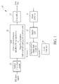
- FIG. 1 illustrates a diagram of an apparatus 10 for performing phase shift control for timing recovery in an electronic device according to an embodiment of the present invention, where the apparatus 10 may comprise at least one portion (e.g. a portion or all) of the electronic device.
- the apparatus 10 may comprise a portion of the electronic device mentioned above, and more particularly, can be at least one hardware circuit such as at least one integrated circuit (IC) within the electronic device and associated circuits thereof.
- the apparatus 10 can be the whole of the electronic device mentioned above.
- the apparatus 10 may comprise a system comprising the electronic device mentioned above (e.g. an audio/video system comprising the electronic device).
- Examples of the electronic device may include, but not limited to, a mobile phone (e.g. a multifunctional mobile phone), a tablet, and a personal computer such as a laptop computer.
- the apparatus 10 may comprise a sampling circuit 12 (labeled "ADC (2-way interleave / 4-way interleave / 8-way interleave) or Edge/Data Samplers (Full-rate / Half-rate / Quarter-rate / Oct-rate)" in FIG. 1 , for better comprehension) that may be implemented with one of various types of sampling architectures.
- the sampling circuit 12 may comprise Analog-to-Digital Converters (ADCs) of one of the 2-way interleave architecture, the 4-way interleave architecture, and the 8-way interleave architecture.
- the sampling circuit 12 may comprise edge/data samplers of one of the Full-rate architecture, the Half-rate (i.e.
- the apparatus 10 may comprise an analog front-end circuit 11, a deserializer 13, a phase detector 14, a digital lower pass filter (LPF) 15, and at least one digital control phase shift oscillator (e.g. one or more digital control phase shift oscillators (DCPSOs)) that can be collectively referred to as the digital control phase shift oscillator 16, and may further comprise a clock generator 18.
- DCPSOs digital control phase shift oscillators
- the analog front-end circuit 11, the sampling circuit 12, the deserializer 13, the phase detector 14, the digital LPF 15, the digital control phase shift oscillator 16, and the clock generator 18 may be positioned in a receiver (RX) of the electronic device.
- the receiver may receive a receiver input signal (i.e. RX input signal) to obtain data carried by the receiver input signal.
- a processing circuit in the electronic device may be coupled to the receiver through at least one data terminal (e.g. one or more data terminals) of the receiver, such as that of a data bus of the receiver, for performing further processing on the data output from the data bus.
- the apparatus 10 may comprise only a portion of the architecture shown in FIG. 1 .
- the analog front-end circuit 11 and the deserializer 13 may be optional.
- internal components of the digital control phase shift oscillator 16 may comprise an oscillator, and may further comprise at least one mixing circuit (e.g. one or more mixing circuits) that is electrically connected to the oscillator.
- the oscillator may be a ring oscillator, and may comprise a plurality of stages, which may be regarded as the oscillator circuit of the oscillator.
- the oscillator may generate one or more output signals, and the digital control phase shift oscillator 16 may shift the phase of any output signal within the one or more output signals.
- the digital control phase shift oscillator 16 may output one or more of the output signals having N phases (labeled "N-phases" in FIG.
- the aforementioned at least one mixing circuit may comprise a set of clock receiving terminals that is arranged to obtain a set of clock signals corresponding to a set of phases, such as those having X phases (labeled "X-phases" in FIG. 1 , for better comprehension), where the notation "X” may represent a positive integer.
- the clock generator 18 may generate the set of clock signals such as those having the X phases, and output the set of clock signals to the digital control phase shift oscillator 16.
- the aforementioned at least one mixing circuit may perform phase shift control on the output signal of the oscillator.
- the aforementioned at least one mixing circuit may control a phase shift of the output signal of the oscillator by selectively combining the set of clock signals of the clock generator 18 into the oscillator within the digital control phase shift oscillator 16 according to a set of digital control signals from the digital LPF 15, where the phase shift corresponds to the set of digital control signals, and the set of digital control signals carries a set of digital weightings for selectively mixing the set of clock signals.
- the sampling circuit 12 may perform timing recovery and sampling on the receiver input signal according to the output signals of the digital control phase shift oscillator 16 (e.g. the aforementioned output signal of the oscillator therein) to reproduce the data from the receiver input signal, where the loop in the architecture shown in FIG. 1 (e.g. the loop formed with the sampling circuit 12, the deserializer 13, the phase detector 14, the digital LPF 15, and the digital control phase shift oscillator 16) may be regarded as a timing recovery loop, and the reproduced data may be reproduced at the aforementioned at least one data terminal of the receiver, such as the data terminals of the data bus of this embodiment.
- the set of digital control signals may be generated according to feedback signals from the data bus.
- the digital LPF 15 may perform digital low pass filtering on derivatives of the feedback signals to generate the set of digital control signals.
- the phase detector 14 may perform phase detection on the feedback signals from the data bus of the receiver to generate phase detection results, where the derivatives of the feedback signals may comprise the phase detection results.
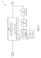
- FIG. 2 illustrates a diagram of an apparatus 10' for performing phase shift control for timing recovery in an electronic device according to an embodiment of the present invention, where the apparatus 10' of this embodiment may comprise some of the components in the architecture shown in FIG. 1 .
- the analog front-end circuit 11 and the deserializer 13 mentioned above may be omitted in this embodiment.
- the sampling circuit 12 may directly receive the receiver input signal, and the data bus may become serial (rather than parallel) in this embodiment.
- the phase detector 14 may be electrically connected to the sampling circuit 12, directly.
- the processing circuit in the electronic device may be coupled to the receiver through the aforementioned at least one data terminal of the receiver, such as the data terminal of the data bus of this embodiment, for performing further processing on the data output from the data bus.
- the sampling circuit 12 may perform timing recovery and sampling on the receiver input signal according to the output signals of the digital control phase shift oscillator 16 (e.g. the aforementioned output signal of the oscillator therein) to reproduce the data from the receiver input signal, where the loop in the architecture shown in FIG. 2 (e.g. the loop formed with the sampling circuit 12, the phase detector 14, the digital LPF 15, and the digital control phase shift oscillator 16) may be regarded as a timing recovery loop, and the reproduced data may be reproduced at the aforementioned at least one data terminal of the receiver, such as the data terminal of the data bus of this embodiment.
- the set of digital control signals may be generated according to a feedback signal from the data bus.
- the digital LPF 15 may perform digital low pass filtering on derivatives of the feedback signal to generate the set of digital control signals.
- the phase detector 14 may perform phase detection on the feedback signal from the data bus of the receiver to generate phase detection results, where the derivatives of the feedback signal may comprise the phase detection results.
- the digital control phase shift oscillator (DCPSO) 16 may be implemented according to the teachings in the U.S. Non-provisional Application No. 14/968,926 (e.g. an apparatus for performing phase shift control in an electronic device in one or more of the embodiments of the U.S. Non-provisional Application No. 14/968,926 , such as the apparatus 100 shown in FIG. 1 thereof, the architecture shown in any of FIGS. 3-4 thereof, the DCPSO shown in any of FIGS. 5-6 thereof, the apparatus 100SE shown in FIG. 7 thereof, the apparatus 100DF shown in FIG. 8 thereof, the apparatus 100SE' shown in FIG. 9 thereof, or the apparatus 100DF' shown in FIG. 10 thereof).
- the U.S. Non-provisional Application No. 14/968,926 for some implementation details.
- the present invention apparatus e.g. the apparatus 10 or the apparatus 10'
- the associated method e.g. a method for controlling operations of the apparatus 10 or the apparatus 10'
- the present invention method and the associated apparatus can achieve lower power consumption, smaller area, and better timing recovery. As a result, the related art problems may no longer be an issue.
- FIG. 3 illustrates a current mode control scheme involved with the digital control phase shift oscillator 16 shown in any of FIGS. 1-2 according to an embodiment of the present invention, where the stages 310-1, 310-2, ..., and 310-N s can be taken as an example of the plurality of stages within the digital control phase shift oscillator 16 shown in any of FIGS. 1-2 .
- each stage of the plurality of stages in the digital control phase shift oscillator 16, such as any of the stages 310-1, 310-2, ..., and 310-N s shown in FIG. 3 may comprise a current mode amplifier.
- each stage of the plurality of stages in the digital control phase shift oscillator 16 may comprise a voltage mode amplifier.
- each stage of the plurality of stages may comprise a differential amplifier.
- each stage of the plurality of stages may comprise a single-end amplifier.
- the aforementioned at least one mixing circuit such as the injection circuits INJ+ and INJ- shown in FIG. 3 may comprise a set of adjustable current sources, such as the two current sources shown around the uppermost of FIG. 3 and the two current sources shown around the lowermost of FIG. 3 , and may further comprise a set of switching units, such as those next to the adjustable current sources shown in FIG. 3 , respectively.
- the set of switching units is coupled between the set of adjustable current sources and the oscillator circuit (which may comprise the plurality of stages) of this embodiment, and more particularly, is coupled between the set of adjustable current sources and at least one stage (e.g.
- the set of clock receiving terminals for obtaining the set of clock signals can be the switching control terminals of these switching units, respectively.
- the clock signal ck( ⁇ + ⁇ * (0 / N x )) having the phase of ( ⁇ + ⁇ * (0 / N x )), the clock signal ck( ⁇ + ⁇ * 1 / N x )) having the phase of ( ⁇ + ⁇ * (/ N x )), the clock signal ck( ⁇ * (0 / N x )) having the phase of ( ⁇ * (0 / N x )), and the clock signal ck( ⁇ * (1 / N x )) having the phase of ( ⁇ * (1 1 N x )) that are shown in FIG. 3 can be taken as an example of the set of clock signals.
- the apparatus 10 may utilize the set of adjustable current sources respectively corresponding to the set of clock signals such as the clock signal ck( ⁇ + ⁇ * (0 / N x )), the clock signal ck( ⁇ + ⁇ * (1 / N x )), the clock signal ck( ⁇ * (0 / N X )), and the clock signal ck( ⁇ * (1 / N X )), to selectively mix the set of clock signals into the oscillator circuit according to the set of digital weighting control signals.
- the set of adjustable current sources respectively corresponding to the set of clock signals such as the clock signal ck( ⁇ + ⁇ * (0 / N x )), the clock signal ck( ⁇ + ⁇ * (1 / N x )), the clock signal ck( ⁇ * (0 / N X )), and the clock signal ck( ⁇ * (1 / N X )
- the set of digital weighting control signals of this embodiment may carry the set of digital weightings such as the digital weightings ⁇ (1 - W), W ⁇ , ⁇ (1 - W), W ⁇ , and therefore, the set of adjustable current sources respectively corresponding to the set of clock signals such as the clock signal ck( ⁇ + ⁇ * (0 / N X )), the clock signal ck( ⁇ + ⁇ * (1 / N X )), the clock signal ck( ⁇ * (0 / N X )), and the clock signal ck( ⁇ * (1 N X )) may generate the currents of ((1 - W) * I), (W * I), ((1 - W) * I), and (W * I), respectively.
- each adjustable current source of the set of adjustable current sources selectively mixes a corresponding clock signal of the set of clock signals, such as the corresponding clock signal within the clock signal ck( ⁇ + ⁇ * (0 N X )), the clock signal ck( ⁇ + ⁇ * (1 / N X )), the clock signal ck( ⁇ * (0 / N X )), and the clock signal ck( ⁇ * (1 / N X )), into the oscillator circuit according to a corresponding digital weighting control signal of the set of digital weighting control signals, such as the corresponding digital weighting control signal within the digital weighting control signals carrying the digital weightings ⁇ (1 - W), W ⁇ , ⁇ (1-W), W ⁇ .
- each stage of the plurality of stages within the digital control phase shift oscillator 16, such as any of the stages 310-1, 310-2, ..., and 310-N S shown in FIG. 3 may comprise a differential amplifier, where at least one portion (e.g. a portion or all) of the set of differential output signals S_OUT+ and S_OUT- shown in FIG. 3 , such as any or both of the differential output signals S_OUT+ and S_OUT-, can be taken as an example of the output signal(s) in the embodiments shown in FIGS. 1-2 .
- the set of differential output signals S_OUT+ and S_OUT- shown in FIG. 3 such as any or both of the differential output signals S_OUT+ and S_OUT-
- each stage of the plurality of stages within the digital control phase shift oscillator 16 such as any of the stages 310-1, 310-2, ..., and 310-N S shown in FIG. 3 , may comprise a single-end amplifier.
- stages 310-1, 310-2, ..., and 310-N S shown in FIG. 3 may comprise a single-end amplifier.
- the number N S of stages within the stages 310-1, 310-2, ..., and 310-N S may be unrelated to the number N of phases within the N phases mentioned above.
- the number N S of stages within the stages 310-1, 310-2, ..., and 310-N S of some embodiments may be different from the number N of phases within the N phases. This is for illustrative purposes only, and is not meant to be a limitation of the present invention.
- the number N S of stages within the stages 310-1, 310-2, ..., and 310-N s may be the same as the number N of phases within the N phases.
- phase parameter N X regarding the phases of some clock signals described above (e.g. the clock signal ck( ⁇ + ⁇ * (0 / N X )) having the phase of ( ⁇ + ⁇ * (0 N X )), the clock signal ck( ⁇ + ⁇ * (1 / N X )) having the phase of ( ⁇ + ⁇ * (/ N X )), the clock signal ck( ⁇ * (0 / N X )) having the phase of ( ⁇ * (0 / N X )), and the clock signal ck( ⁇ * (1 / N X )) having the phase of ( ⁇ * (1 / N X )) that are shown in FIG. 3 ) may be related to the number X of phases within the X phases mentioned above.
- phase parameter N X regarding the phases of these clock signals in some embodiments may be the same as the number X of phases within the X phases. This is for illustrative purposes only, and is not meant to be a limitation of the present invention. In some other embodiments, the phase parameter N X regarding the phases of these clock signals may be different from the number X of phases within the X phases.
- phase parameter N X regarding the phases of some clock signals described above (e.g. the clock signal ck( ⁇ + ⁇ * (0 / N X )) having the phase of ( ⁇ + ⁇ * (0 / N X )), the clock signal ck( ⁇ + ⁇ * (1 / N X )) having the phase of ( ⁇ + ⁇ * (/ N X )), the clock signal ck( ⁇ * (0 / N X )) having the phase of ( ⁇ * (0 / N X )), and the clock signal ck( ⁇ * (1 / N X )) having the phase of ( ⁇ * (1 / N X )) that are shown in FIG. 3 ) may be unrelated to the number N of phases within the N phases mentioned above.
- phase parameter N X regarding the phases of these clock signals in some embodiments may be different from the number N of phases within the N phases. This is for illustrative purposes only, and is not meant to be a limitation of the present invention. In some other embodiments, the phase parameter N X regarding the phases of these clock signals may be the same as the number N of phases within the N phases.
- FIG. 4 illustrates a sub-circuit of one of the injection circuits INJ+ and INJ-shown in FIG. 3 according to an embodiment of the present invention.
- the sub-circuit shown in FIG. 4 can be utilized for implementing any of the two branches in the injection circuit INJ+ (e.g. the left branch and the right branch of the injection circuit INJ+, respectively), and can be utilized for implementing any of the two branches in the injection circuit INJ- (e.g. the left branch and the right branch of the injection circuit INJ-, respectively).
- the two branches in the injection circuit INJ+ e.g. the left branch and the right branch of the injection circuit INJ+, respectively
- the injection circuit INJ- e.g. the left branch and the right branch of the injection circuit INJ-
- a first sub-circuit, a second sub-circuit, a third sub-circuit, and a fourth sub-circuit can be utilized for implementing the left branch of the two branches in the injection circuit INJ+, the right branch of the two branches in the injection circuit INJ+, the left branch of the two branches in the injection circuit INJ-, and the right branch of the two branches in the injection circuit INJ-, respectively.
- the terminal VB thereof may receive the clock signal ck( ⁇ + ⁇ * (0 / N X )) having the phase of ( ⁇ + ⁇ * (0 / N X )), and the (N R + 1) switches ⁇ MB(0), MB(1), ..., MB(N R ) ⁇ thereof (e.g. (N R + 1) Metal Oxide Semiconductor Field Effect Transistors (MOSFETs)) may perform switching operations according to the clock signal ck( ⁇ + ⁇ * (0 / N X )).
- MOSFETs Metal Oxide Semiconductor Field Effect Transistors
- the terminals ⁇ B[0], B[1], ..., B[N R ] ⁇ thereof may receive the digital weighting control signals corresponding to the left branch of the two branches in the injection circuit INJ+, and the digital weighting (1 - W) for this branch may be equivalent to the ratio of the number N R-ON (1) of turn-on switch(es) within the (N R + 1) switches ⁇ MS(0), MS(1), ..., MS(N R ) ⁇ thereof (e.g.
- N R + 1 MOSFETs to the number (N R + 1) of all of these (N R + 1) switches ⁇ MS(0),MS(1), ..., MS(N R ) ⁇ , where the notation "N R-ON (1)" may represent an integer that falls within the range of the interval [0, N R + 1].
- the digital weighting (1 - W) for this branch is not equal to zero.
- the number N R-ON (1) may be a positive integer that falls within the range of the interval [1, N R + 1].
- each of the digital weighting (1 - W) for this branch and the digital weighting W for the other branch within the two branches in the injection circuit INJ+ is not equal to zero.
- the number N R-ON (1) may be a positive integer that falls within the range of the interval [1, N R ].
- the terminal VB thereof may receive the clock signal ck( ⁇ + ⁇ * 1 / N X )) having the phase of ( ⁇ + ⁇ * (/ N X )), and the (N R +1) switches ⁇ MB(0), MB(1), ..., MB(N R ) ⁇ thereof (e.g. (N R + 1) MOSFETs) may perform switching operations according to the clock signal ck( ⁇ + ⁇ * (1 / N X )).
- terminals ⁇ B[0], B[1], ..., B[N R ] ⁇ thereof may receive the digital weighting control signals corresponding to the right branch of the two branches in the injection circuit INJ+, and the digital weighting W for this branch may be equivalent to the ratio of the number N R-ON (2) of turn-on switch(es) within the (N R + 1) switches ⁇ MS(0),MS(1), ..., MS(N R ) ⁇ thereof (e.g.
- N R + 1) MOSFETs to the number (N R + 1) of all of these (N R + 1) switches ⁇ MS(0),MS(1), ..., MS(NR) ⁇ , where the notation "N R-ON (2)" may represent an integer that falls within the range of the interval [0, N R + 1].
- the digital weighting W for this branch is not equal to zero.
- the number N R-ON (2) may be a positive integer that falls within the range of the interval [1, N R + 1].
- each of the digital weighting W for this branch and the digital weighting (1 - W) for the other branch within the two branches in the injection circuit INJ+ is not equal to zero.
- the number N R-ON (2) may be a positive integer that falls within the range of the interval [1, N R ].
- the terminal VB thereof may receive the clock signal ck( ⁇ * (0 / N X )) having the phase of ( ⁇ * (0 / N X )), and the (N R + 1) switches ⁇ MB(0), MB(1), ..., MB(N R ) ⁇ thereof (e.g. (N R + 1) MOSFETs) may perform switching operations according to the clock signal ck( ⁇ * (0 / N X )).
- the terminals ⁇ B[0], B[1], ..., B[N R ] ⁇ thereof may receive the digital weighting control signals corresponding to the left branch of the two branches in the injection circuit INJ-, and the digital weighting (1 - W) for this branch may be equivalent to the ratio of the number N R-ON (3) of turn-on switch(es) within the (N R + 1) switches ⁇ MS(0), MS(1), ..., MS(N R ) ⁇ thereof (e.g.
- N R + 1) MOSFETs to the number (N R + 1) of all of these (N R + 1) switches ⁇ MS(0),MS(1), ..., MS(N R ) ⁇ , where the notation "N R-ON (3)" may represent an integer that falls within the range of the interval [0, N R + 1].
- the digital weighting (1 - W) for this branch is not equal to zero.
- the number N R-ON (3) may be a positive integer that falls within the range of the interval [1, N R + 1].
- each of the digital weighting (1 - W) for this branch and the digital weighting W for the other branch within the two branches in the injection circuit INJ- is not equal to zero.
- the number N R-ON (3) may be a positive integer that falls within the range of the interval [1, N R ].
- the terminal VB thereof may receive the clock signal ck( ⁇ * (1 / N X )) having the phase of ( ⁇ * (1 / N X )), and the (N R + 1) switches ⁇ MB(0), MB(1), ..., MB(N R ) ⁇ thereof (e.g. (N R + 1) MOSFETs) may perform switching operations according to the clock signal ck( ⁇ * (1 / N X )).
- the terminals ⁇ B[0], B[1], ..., B[N R ] ⁇ thereof may receive the digital weighting control signals corresponding to the right branch of the two branches in the injection circuit INJ-, and the digital weighting W for this branch may be equivalent to the ratio of the number N R-ON (4) of turn-on switch(es) within the (N R + 1) switches ⁇ MS(0), MS(1), ..., MS(N R ) ⁇ thereof (e.g.
- N R + 1 MOSFETs
- N R + 1 MOSFETs
- the number N R + 1 MOSFETs to the number (N R + 1) of all of these (N R + 1) switches ⁇ MS(0),MS(1), ..., MS(NR) ⁇
- the notation "N R - ON (4)" may represent an integer that falls within the range of the interval [0, N R + 1].
- the digital weighting W for this branch is not equal to zero.
- the number N R-ON (4) may be a positive integer that falls within the range of the interval [1, N R + 1].
- each of the digital weighting W for this branch and the digital weighting (1 - W) for the other branch within the two branches in the injection circuit INJ- is not equal to zero.
- the number N R-ON (4) may be a positive integer that falls within the range of the interval [1, N R ].
- each of the first sub-circuit, the second sub-circuit, the third sub-circuit, and the fourth sub-circuit mentioned above can be regarded as a current sink.
- the 3 may selectively mix the set of clock signals such as the clock signal ck( ⁇ + ⁇ * (0 / N X )), the clock signal ck( ⁇ + ⁇ * (1 / N X )), the clock signal ck( ⁇ * (0 / N X )), and the clock signal ck( ⁇ * (1 / N X )) into the oscillator circuit according to the set of digital weighting control signals such as the digital weighting control signals carrying the digital weightings ⁇ (1 - W), W ⁇ , ⁇ (1 - W), W ⁇ , respectively.
- the set of digital weighting control signals such as the digital weighting control signals carrying the digital weightings ⁇ (1 - W), W ⁇ , ⁇ (1 - W), W ⁇ , respectively.
- the number (N R + 1) of sub-paths corresponding to the (N R + 1) switches ⁇ MS(0),MS(1), ..., MS(N R ) ⁇ may be unrelated to the number N of phases within the N phases mentioned above.
- the number (N R + 1) of sub-paths corresponding to the (N R + 1) switches ⁇ MS(0),MS(1), ..., MS(N R ) ⁇ of some embodiments may be different from the number N of phases within the N phases. This is for illustrative purposes only, and is not meant to be a limitation of the present invention.
- the number (N R + 1) of sub-paths corresponding to the (N R + 1) switches ⁇ MS(0), MS(1), ..., MS(N R ) ⁇ may be the same as the number N of phases within the N phases.
- the number (N R + 1) of sub-paths corresponding to the (N R + 1) switches ⁇ MS(0),MS(1), ..., MS(N R ) ⁇ may be unrelated to the phase parameter N X regarding the phases of some clock signals described above (e.g.
- the number (N R + 1) of sub-paths corresponding to the (N R + 1) switches ⁇ MS(0),MS(1), ..., MS(N R ) ⁇ of some embodiments may be different from the phase parameter N X regarding the phases of these clock signals.
- the number (N R + 1) of sub-paths corresponding to the (N R + 1) switches ⁇ MS(0),MS(1), ..., MS(N R ) ⁇ may be the same as the phase parameter N X regarding the phases of these clock signals.
- the phase shift of the output signal of the oscillator (more particularly, the oscillator circuit) within the digital control phase shift oscillator 16 may be controlled by selectively combining the set of clock signals into a specific stage of the plurality of stages according to the set of digital control signals.
- the phase shift of the output signal of the oscillator (more particularly, the oscillator circuit) within the digital control phase shift oscillator 16 may be controlled by injecting at least one portion (e.g. a portion or all) of the set of clock signals into the specific stage according to the set of digital control signals, where the signal count of the aforementioned at least one portion of the set of clock signals corresponds to the set of digital weightings carried by the set of digital control signals.
- the phase shift of the output signal of the oscillator (more particularly, the oscillator circuit) within the digital control phase shift oscillator 16 may be controlled by selectively combining the set of clock signals into the specific stage of the plurality of stages according to the set of digital control signals and by selectively combining another set of clock signals into another stage of the plurality of stages according to another set of digital control signals.
- the phase shift of the output signal of the oscillator (more particularly, the oscillator circuit) within the digital control phase shift oscillator 16 may be controlled by injecting at least one portion (e.g. a portion or all) of the set of clock signals into the specific stage of the plurality of stages according to the set of digital control signals and by injecting at least one portion (e.g.
- the other set of clock signals may be equivalent to the set of clock signals.
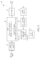
- FIG. 5 is a diagram of an apparatus 20 for performing phase shift control for timing recovery in an electronic device according to another embodiment of the present invention, where the apparatus 20 of this embodiment may comprise some of the components in the architecture shown in FIG. 1 .
- the apparatus 20 may comprise a hybrid LPF circuit 25 having analog phase rotators embedded therein (labeled "LPF + Analog Phase Rotator" in FIG. 5 , for brevity) that replaces the digital LPF 15 mentioned above, and may comprise a voltage control phase shift oscillator 26 that replaces the digital control phase shift oscillator 16 mentioned above.
- LPF + Analog Phase Rotator analog phase rotators embedded therein
- the set of digital control signals mentioned above can be replaced by a set of analog control signals from the hybrid LPF circuit 25, where the phase shift corresponds to the set of analog control signals, and the set of analog control signals carries a set of analog weightings that replaces the set of digital weightings mentioned above, for selectively mixing the set of clock signals.
- the voltage control phase shift oscillator 26 may comprise a set of clock receiving terminals such as that in the digital control phase shift oscillator 16, and may comprise a plurality of stages such as that in the digital control phase shift oscillator 16, and may further comprise one or more mixing circuits having analog control terminals (e.g. one or more injection circuits having the analog control terminals).
- the aforementioned one or more mixing circuits having analog control terminals may be arranged for selectively mixing the set of clock signals into one or more of the plurality of stages in the voltage control phase shift oscillator 26 according to the set of analog control signals.
- the loop in the architecture shown in FIG. 5 e.g. the loop formed with the sampling circuit 12, the deserializer 13, the phase detector 14, the hybrid LPF circuit 25, and the voltage control phase shift oscillator 26
- the loop in the architecture shown in FIG. 5 e.g. the loop formed with the sampling circuit 12, the deserializer 13, the phase detector 14, the hybrid LPF circuit 25, and the voltage control phase shift oscillator 26
- the loop in the architecture shown in FIG. 5 e.g. the loop formed with the sampling circuit 12, the deserializer 13, the phase detector 14, the hybrid LPF circuit 25, and the voltage control phase shift oscillator 26
- the loop in the architecture shown in FIG. 5 may be regarded as a timing recovery loop.
- similar descriptions for this embodiment are not repeated in detail here.
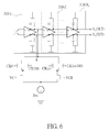
- FIG. 6 illustrates a control scheme involved with the voltage control phase shift oscillator 26 shown in FIG. 5 according to an embodiment of the present invention.
- the injection circuits INJ+ and INJ- shown in FIG. 3 may be replaced by analog injection circuits such as that in the lower half of the architecture shown in FIG. 6 , for implementing the voltage control phase shift oscillator 26 shown in FIG. 5 .
- the clock signal CK0 having the phase of 0°, the clock signal CK180 having the phase of 180°, the clock signal CK(x) having the phase of x°, and the clock signal CK(x + 180) having the phase of (x + 180)° can be taken as examples of the set of clock signals, and the clock terminals for receiving the clock signals CK0, CK180, CK(x), and CK(x + 180) can be taken as examples of the set of clock receiving terminals of the voltage control phase shift oscillator 26.
- the voltage control terminals VC and VCB can be taken as examples of the analog control terminals of the aforementioned one or more mixing circuits in the voltage control phase shift oscillator 26.
- different branches of the analog injection circuits may share the current I WI of the current source I WI that is electrically connected to these branches. For brevity, similar descriptions for this embodiment are not repeated in detail here.
Landscapes
- Engineering & Computer Science (AREA)
- Power Engineering (AREA)
- Stabilization Of Oscillater, Synchronisation, Frequency Synthesizers (AREA)
Abstract

Description
- The present invention relates to a method and apparatus for performing phase shift control for timing recovery in an electronic device according to the pre-characterizing clauses of
claims - In ultra-high speed Serializer/Deserializer (SerDes) or Analog-to-Digital Convertor (ADC) applications, the sub-rate (e.g. half-rate, quarter-rate, oct-rate, etc.) Serdes or interleave ADC architecture may have become the main stream since it is possible to reduce the samplers timing budget or the noise specification requirement. While the techniques progresses, however, some problems such as some side effects may occur. For example, the related art may suffer from one or more of high power consumption, large area, and poor timing recovery. Thus, how to achieve lower power consumption, smaller area, and better timing recovery has become an important issue to be solved.
- This in mind, the present invention aims at providing a method and apparatus for performing phase shift control for timing recovery in an electronic device that guarantee the overall performance of the electronic device.
- This is achieved by a method and apparatus for performing phase shift control for timing recovery in an electronic device according to the pre-characterizing clauses of
claims - In one aspect, the disclosure features a method for performing phase shift control in an electronic device, where the method comprises the steps of: obtaining a set of clock signals corresponding to a set of phases; and controlling a phase shift of an output signal of an oscillator by selectively mixing the set of clock signals into the oscillator according to a set of digital control signals, wherein the phase shift corresponds to the set of digital control signals, and the set of digital control signals carries a set of digital weightings for selectively mixing the set of clock signals. More particularly, the oscillator may comprise a plurality of stages, and the step of controlling the phase shift of the output signal of the oscillator by selectively mixing the set of clock signals into the oscillator according to the set of digital control signals may further comprise: controlling the phase shift of the output signal of the oscillator by selectively mixing the set of clock signals into a specific stage of the plurality of stages according to the set of digital control signals.
- In one aspect, the disclosure features an apparatus for performing phase shift control in an electronic device, where the apparatus comprises at least one portion of the electronic device. The apparatus comprises an oscillator, and further comprises at least one mixing circuit that is electrically connected to the oscillator. The oscillator is arranged to generate an output signal. In addition, the aforementioned at least one mixing circuit comprises a set of clock receiving terminals that is arranged to obtain a set of clock signals corresponding to a set of phases. Additionally, the aforementioned at least one mixing circuit is arranged to perform phase shift control on the output signal of the oscillator. For example, the aforementioned at least one mixing circuit may control a phase shift of the output signal of the oscillator by selectively mixing the set of clock signals into the oscillator according to a set of digital control signals, wherein the phase shift corresponds to the set of digital control signals, and the set of digital control signals carries a set of digital weightings for selectively mixing the set of clock signals. More particularly, the oscillator may comprise a plurality of stages, and the aforementioned at least one mixing circuit may control the phase shift of the output signal of the oscillator by selectively mixing the set of clock signals into a specific stage of the plurality of stages according to the set of digital control signals.
- In one aspect, the disclosure features a method for performing phase shift control for timing recovery in an electronic device, where the method may comprise: generating an output signal of an oscillator, wherein a phase shift of the output signal of the oscillator is controlled by selectively combining a set of clock signals into the oscillator according to a set of digital control signals, and the set of clock signals is obtained from a clock generator, wherein the phase shift corresponds to the set of digital control signals, and the set of digital control signals carries a set of digital weightings for selectively mixing the set of clock signals; and performing timing recovery and sampling on a receiver input signal of a receiver in the electronic device according to the output signal of the oscillator to reproduce data from the receiver input signal, wherein the reproduced data are reproduced at a data bus of the receiver, and the set of digital control signals is generated according to feedback signals from the data bus. For example, the method may further comprise utilizing a digital low pass filter to perform digital low pass filtering on derivatives of the feedback signals to generate the set of digital control signals. For example, the method may further comprise utilizing a phase detector to perform phase detection on the feedback signals from the data bus of the receiver to generate phase detection results, wherein the derivatives of the feedback signals comprise the phase detection results. In some embodiments, the timing recovery and sampling may be performed with Analog-to-Digital Converters (ADCs) of an interleave ADC architecture or edge/data samplers of a Serializer/Deserializer (SerDes) architecture.
- In one aspect, the disclosure features an apparatus for performing phase shift control for timing recovery in an electronic device, where the apparatus may comprise at least one portion (e.g. a portion or all) of the electronic device. For example, the apparatus may comprise an oscillator, and further comprise at least one mixing circuit that is electrically connected to the oscillator. The oscillator is arranged to generate an output signal, and the aforementioned at least one mixing circuit comprises a set of clock receiving terminals that is arranged to obtain a set of clock signals. In addition, the aforementioned at least one mixing circuit is arranged to perform phase shift control on the output signal of the oscillator. For example, the aforementioned at least one mixing circuit may control a phase shift of the output signal of the oscillator by selectively combining the set of clock signals into the oscillator according to a set of digital control signals, wherein the phase shift corresponds to the set of digital control signals, and the set of digital control signals carries a set of digital weightings for selectively mixing the set of clock signals. Additionally, the apparatus may further comprise a clock generator, and comprise a sampling circuit that is positioned in a receiver in the electronic device. The clock generator is arranged to generate the set of clock signals, and the sampling circuit is arranged to perform timing recovery and sampling on a receiver input signal of the receiver according to the output signal of the oscillator to reproduce data from the receiver input signal, wherein the reproduced data are reproduced at a data bus of the receiver, and the set of digital control signals is generated according to feedback signals from the data bus. For example, the apparatus may further comprise a digital low pass filter arranged to perform digital low pass filtering on derivatives of the feedback signals to generate the set of digital control signals. For example, the apparatus may further comprise a phase detector arranged to perform phase detection on the feedback signals from the data bus of the receiver to generate phase detection results, wherein the derivatives of the feedback signals comprise the phase detection results. In some embodiments, the sampling circuit may be implemented with ADCs of an interleave ADC architecture or edge/data samplers of a SerDes architecture.
- It is an advantage of the present invention that the present invention method and the associated apparatus can guarantee the overall performance of the electronic device. For example, the present invention method and the associated apparatus can maintain linearity of the hardware circuitry for a wide frequency range. In comparison with the related art, the present invention method and the associated apparatus can achieve lower power consumption, smaller area, and better timing recovery. As a result, the related art problems may no longer be an issue.
- In the following, the invention is further illustrated by way of example, taking reference to the accompanying drawings. Thereof
- FIG. 1
- is a diagram of an apparatus for performing phase shift control for timing recovery in an electronic device according to an embodiment of the present invention,
- FIG. 2
- is a diagram of an apparatus for performing phase shift control for timing recovery in an electronic device according to another embodiment of the present invention,
- FIG. 3
- illustrates a current mode control scheme involved with the digital control phase shift oscillator shown in any of
FIGS. 1-2 according to an embodiment of the present invention, - FIG. 4
- illustrates a sub-circuit of one of the injection circuits shown in
FIG. 3 according to an embodiment of the present invention, - FIG. 5
- is a diagram of an apparatus for performing phase shift control for timing recovery in an electronic device according to another embodiment of the present invention, and
- FIG. 6
- illustrates a control scheme involved with the voltage control phase shift oscillator shown in
FIG. 5 according to an embodiment of the present invention. - Certain terms are used throughout the following description and claims, which refer to particular components. As one skilled in the art will appreciate, electronic equipment manufacturers may refer to a component by different names. This document does not intend to distinguish between components that differ in name but not in function. In the following description and in the claims, the terms "include" and "comprise" are used in an open-ended fashion, and thus should be interpreted to mean "include, but not limited to ...". Also, the term "couple" is intended to mean either an indirect or direct electrical connection. Accordingly, if one device is coupled to another device, that connection may be through a direct electrical connection, or through an indirect electrical connection via other devices and connections.
-
FIG. 1 illustrates a diagram of anapparatus 10 for performing phase shift control for timing recovery in an electronic device according to an embodiment of the present invention, where theapparatus 10 may comprise at least one portion (e.g. a portion or all) of the electronic device. For example, theapparatus 10 may comprise a portion of the electronic device mentioned above, and more particularly, can be at least one hardware circuit such as at least one integrated circuit (IC) within the electronic device and associated circuits thereof. In another example, theapparatus 10 can be the whole of the electronic device mentioned above. In another example, theapparatus 10 may comprise a system comprising the electronic device mentioned above (e.g. an audio/video system comprising the electronic device). Examples of the electronic device may include, but not limited to, a mobile phone (e.g. a multifunctional mobile phone), a tablet, and a personal computer such as a laptop computer. - As shown in
FIG. 1 , theapparatus 10 may comprise a sampling circuit 12 (labeled "ADC (2-way interleave / 4-way interleave / 8-way interleave) or Edge/Data Samplers (Full-rate / Half-rate / Quarter-rate / Oct-rate)" inFIG. 1 , for better comprehension) that may be implemented with one of various types of sampling architectures. For example, thesampling circuit 12 may comprise Analog-to-Digital Converters (ADCs) of one of the 2-way interleave architecture, the 4-way interleave architecture, and the 8-way interleave architecture. In another example, thesampling circuit 12 may comprise edge/data samplers of one of the Full-rate architecture, the Half-rate (i.e. 1/2 rate) architecture, the Quarter-rate (i.e. 1/4 rate) architecture, and the Oct-rate (i.e. 1/8 rate) architecture. In addition, theapparatus 10 may comprise an analog front-end circuit 11, adeserializer 13, aphase detector 14, a digital lower pass filter (LPF) 15, and at least one digital control phase shift oscillator (e.g. one or more digital control phase shift oscillators (DCPSOs)) that can be collectively referred to as the digital controlphase shift oscillator 16, and may further comprise aclock generator 18. Additionally, the components of the architecture shown inFIG. 1 (e.g. the analog front-end circuit 11, thesampling circuit 12, thedeserializer 13, thephase detector 14, thedigital LPF 15, the digital controlphase shift oscillator 16, and the clock generator 18) may be positioned in a receiver (RX) of the electronic device. The receiver may receive a receiver input signal (i.e. RX input signal) to obtain data carried by the receiver input signal. For example, a processing circuit in the electronic device may be coupled to the receiver through at least one data terminal (e.g. one or more data terminals) of the receiver, such as that of a data bus of the receiver, for performing further processing on the data output from the data bus. In some embodiments, theapparatus 10 may comprise only a portion of the architecture shown inFIG. 1 . For example, the analog front-end circuit 11 and thedeserializer 13 may be optional. - According to the embodiment shown in
FIG. 1 , internal components of the digital controlphase shift oscillator 16 may comprise an oscillator, and may further comprise at least one mixing circuit (e.g. one or more mixing circuits) that is electrically connected to the oscillator. For example, the oscillator may be a ring oscillator, and may comprise a plurality of stages, which may be regarded as the oscillator circuit of the oscillator. The oscillator may generate one or more output signals, and the digital controlphase shift oscillator 16 may shift the phase of any output signal within the one or more output signals. As a result, the digital controlphase shift oscillator 16 may output one or more of the output signals having N phases (labeled "N-phases" inFIG. 1 , for better comprehension), where the notation "N" may represent a positive integer. In this embodiment, the aforementioned at least one mixing circuit (e.g. one or more mixing circuits) may comprise a set of clock receiving terminals that is arranged to obtain a set of clock signals corresponding to a set of phases, such as those having X phases (labeled "X-phases" inFIG. 1 , for better comprehension), where the notation "X" may represent a positive integer. For example, theclock generator 18 may generate the set of clock signals such as those having the X phases, and output the set of clock signals to the digital controlphase shift oscillator 16. In addition, the aforementioned at least one mixing circuit may perform phase shift control on the output signal of the oscillator. For example, the aforementioned at least one mixing circuit may control a phase shift of the output signal of the oscillator by selectively combining the set of clock signals of theclock generator 18 into the oscillator within the digital controlphase shift oscillator 16 according to a set of digital control signals from thedigital LPF 15, where the phase shift corresponds to the set of digital control signals, and the set of digital control signals carries a set of digital weightings for selectively mixing the set of clock signals. - Based on the architecture shown in
FIG. 1 , thesampling circuit 12 may perform timing recovery and sampling on the receiver input signal according to the output signals of the digital control phase shift oscillator 16 (e.g. the aforementioned output signal of the oscillator therein) to reproduce the data from the receiver input signal, where the loop in the architecture shown inFIG. 1 (e.g. the loop formed with thesampling circuit 12, thedeserializer 13, thephase detector 14, thedigital LPF 15, and the digital control phase shift oscillator 16) may be regarded as a timing recovery loop, and the reproduced data may be reproduced at the aforementioned at least one data terminal of the receiver, such as the data terminals of the data bus of this embodiment. In addition, the set of digital control signals may be generated according to feedback signals from the data bus. For example, thedigital LPF 15 may perform digital low pass filtering on derivatives of the feedback signals to generate the set of digital control signals. More particularly, thephase detector 14 may perform phase detection on the feedback signals from the data bus of the receiver to generate phase detection results, where the derivatives of the feedback signals may comprise the phase detection results. -
FIG. 2 illustrates a diagram of an apparatus 10' for performing phase shift control for timing recovery in an electronic device according to an embodiment of the present invention, where the apparatus 10' of this embodiment may comprise some of the components in the architecture shown inFIG. 1 . In comparison with the architecture shown inFIG. 1 , the analog front-end circuit 11 and thedeserializer 13 mentioned above may be omitted in this embodiment. In addition, thesampling circuit 12 may directly receive the receiver input signal, and the data bus may become serial (rather than parallel) in this embodiment. Additionally, thephase detector 14 may be electrically connected to thesampling circuit 12, directly. For example, the processing circuit in the electronic device may be coupled to the receiver through the aforementioned at least one data terminal of the receiver, such as the data terminal of the data bus of this embodiment, for performing further processing on the data output from the data bus. - Based on the architecture shown in
FIG. 2 , thesampling circuit 12 may perform timing recovery and sampling on the receiver input signal according to the output signals of the digital control phase shift oscillator 16 (e.g. the aforementioned output signal of the oscillator therein) to reproduce the data from the receiver input signal, where the loop in the architecture shown inFIG. 2 (e.g. the loop formed with thesampling circuit 12, thephase detector 14, thedigital LPF 15, and the digital control phase shift oscillator 16) may be regarded as a timing recovery loop, and the reproduced data may be reproduced at the aforementioned at least one data terminal of the receiver, such as the data terminal of the data bus of this embodiment. In addition, the set of digital control signals may be generated according to a feedback signal from the data bus. For example, thedigital LPF 15 may perform digital low pass filtering on derivatives of the feedback signal to generate the set of digital control signals. More particularly, thephase detector 14 may perform phase detection on the feedback signal from the data bus of the receiver to generate phase detection results, where the derivatives of the feedback signal may comprise the phase detection results. - According to some embodiments, such as any of the embodiments respectively shown in
FIGS. 1-2 , the digital control phase shift oscillator (DCPSO) 16 may be implemented according to the teachings in theU.S. Non-provisional Application No. 14/968,926 (e.g. an apparatus for performing phase shift control in an electronic device in one or more of the embodiments of theU.S. Non-provisional Application No. 14/968,926 , such as the apparatus 100 shown inFIG. 1 thereof, the architecture shown in any ofFIGS. 3-4 thereof, the DCPSO shown in any ofFIGS. 5-6 thereof, the apparatus 100SE shown in FIG. 7 thereof, the apparatus 100DF shown in FIG. 8 thereof, the apparatus 100SE' shown in FIG. 9 thereof, or the apparatus 100DF' shown in FIG. 10 thereof). Please refer to theU.S. Non-provisional Application No. 14/968,926 for some implementation details. - With aid of the digital control
phase shift oscillator 16, the present invention apparatus (e.g. theapparatus 10 or the apparatus 10') and the associated method (e.g. a method for controlling operations of theapparatus 10 or the apparatus 10') can guarantee the overall performance of the electronic device. In comparison with the related art, the present invention method and the associated apparatus can achieve lower power consumption, smaller area, and better timing recovery. As a result, the related art problems may no longer be an issue. -
FIG. 3 illustrates a current mode control scheme involved with the digital controlphase shift oscillator 16 shown in any ofFIGS. 1-2 according to an embodiment of the present invention, where the stages 310-1, 310-2, ..., and 310-Ns can be taken as an example of the plurality of stages within the digital controlphase shift oscillator 16 shown in any ofFIGS. 1-2 . In this embodiment, each stage of the plurality of stages in the digital controlphase shift oscillator 16, such as any of the stages 310-1, 310-2, ..., and 310-Ns shown inFIG. 3 , may comprise a current mode amplifier. According to some embodiments, each stage of the plurality of stages in the digital controlphase shift oscillator 16 may comprise a voltage mode amplifier. According to some embodiments, each stage of the plurality of stages may comprise a differential amplifier. According to some embodiments, each stage of the plurality of stages may comprise a single-end amplifier. - According to this embodiment, the aforementioned at least one mixing circuit such as the injection circuits INJ+ and INJ- shown in
FIG. 3 may comprise a set of adjustable current sources, such as the two current sources shown around the uppermost ofFIG. 3 and the two current sources shown around the lowermost ofFIG. 3 , and may further comprise a set of switching units, such as those next to the adjustable current sources shown inFIG. 3 , respectively. For example, the set of switching units is coupled between the set of adjustable current sources and the oscillator circuit (which may comprise the plurality of stages) of this embodiment, and more particularly, is coupled between the set of adjustable current sources and at least one stage (e.g. one or more stages) of the stages 310-1, 310-2, ..., and 310-Ns, where the set of clock receiving terminals for obtaining the set of clock signals can be the switching control terminals of these switching units, respectively. In addition, the clock signal ck(π + π * (0 / Nx)) having the phase of (π + π * (0 / Nx)), the clock signal ck(π + π* 1 / Nx)) having the phase of (π + π * (/ Nx)), the clock signal ck(π * (0 / Nx)) having the phase of ( π * (0 / Nx)), and the clock signal ck(π * (1 / Nx)) having the phase of (π* (1 1 Nx)) that are shown inFIG. 3 can be taken as an example of the set of clock signals. - According to this embodiment, the
apparatus 10 may utilize the set of adjustable current sources respectively corresponding to the set of clock signals such as the clock signal ck(π + π * (0 / Nx)), the clock signal ck(π +π* (1 / Nx)), the clock signal ck(π * (0 / NX)), and the clock signal ck(π * (1 / NX)), to selectively mix the set of clock signals into the oscillator circuit according to the set of digital weighting control signals. For example, the set of digital weighting control signals of this embodiment may carry the set of digital weightings such as the digital weightings {{(1 - W), W}, {(1 - W), W}}, and therefore, the set of adjustable current sources respectively corresponding to the set of clock signals such as the clock signal ck(π + π * (0 / NX)), the clock signal ck(π +π* (1 / NX)), the clock signal ck(π * (0 / NX)), and the clock signal ck(π * (1 NX)) may generate the currents of ((1 - W) * I), (W * I), ((1 - W) * I), and (W * I), respectively. In addition, the set of adjustable current sources is controlled by the set of digital weighting control signals, and each adjustable current source of the set of adjustable current sources selectively mixes a corresponding clock signal of the set of clock signals, such as the corresponding clock signal within the clock signal ck(π + π * (0 NX)), the clock signal ck(π +π* (1 / NX)), the clock signal ck(π * (0 / NX)), and the clock signal ck(π * (1 / NX)), into the oscillator circuit according to a corresponding digital weighting control signal of the set of digital weighting control signals, such as the corresponding digital weighting control signal within the digital weighting control signals carrying the digital weightings {{(1 - W), W}, {(1-W), W}}. - Please note that, in the embodiment shown in
FIG. 3 , each stage of the plurality of stages within the digital controlphase shift oscillator 16, such as any of the stages 310-1, 310-2, ..., and 310-NS shown inFIG. 3 , may comprise a differential amplifier, where at least one portion (e.g. a portion or all) of the set of differential output signals S_OUT+ and S_OUT- shown inFIG. 3 , such as any or both of the differential output signals S_OUT+ and S_OUT-, can be taken as an example of the output signal(s) in the embodiments shown inFIGS. 1-2 . For brevity, similar descriptions for this embodiment are not repeated in detail here. - According to some embodiments, each stage of the plurality of stages within the digital control
phase shift oscillator 16, such as any of the stages 310-1, 310-2, ..., and 310-NS shown inFIG. 3 , may comprise a single-end amplifier. For brevity, similar descriptions for these embodiments are not repeated in detail here. - In general, the number NS of stages within the stages 310-1, 310-2, ..., and 310-NS may be unrelated to the number N of phases within the N phases mentioned above. For example, the number NS of stages within the stages 310-1, 310-2, ..., and 310-NS of some embodiments may be different from the number N of phases within the N phases. This is for illustrative purposes only, and is not meant to be a limitation of the present invention. In some other embodiments, the number NS of stages within the stages 310-1, 310-2, ..., and 310-Ns may be the same as the number N of phases within the N phases.
- In addition, the phase parameter NX regarding the phases of some clock signals described above (e.g. the clock signal ck(π + π * (0 / NX)) having the phase of ( π + π* (0 NX)), the clock signal ck(π +π* (1 / NX)) having the phase of (π + π * (/ NX)), the clock signal ck(π * (0 / NX)) having the phase of (π * (0 / NX)), and the clock signal ck(π * (1 / NX)) having the phase of (π * (1 / NX)) that are shown in
FIG. 3 ) may be related to the number X of phases within the X phases mentioned above. For example, the phase parameter NX regarding the phases of these clock signals in some embodiments may be the same as the number X of phases within the X phases. This is for illustrative purposes only, and is not meant to be a limitation of the present invention. In some other embodiments, the phase parameter NX regarding the phases of these clock signals may be different from the number X of phases within the X phases. - Additionally, the phase parameter NX regarding the phases of some clock signals described above (e.g. the clock signal ck(π + π * (0 / NX)) having the phase of (π + π * (0 / NX)), the clock signal ck(π +π* (1 / NX)) having the phase of (π + π * (/ NX)), the clock signal ck(π * (0 / NX)) having the phase of (π * (0 / NX)), and the clock signal ck(π * (1 / NX)) having the phase of (π * (1 / NX)) that are shown in
FIG. 3 ) may be unrelated to the number N of phases within the N phases mentioned above. For example, the phase parameter NX regarding the phases of these clock signals in some embodiments may be different from the number N of phases within the N phases. This is for illustrative purposes only, and is not meant to be a limitation of the present invention. In some other embodiments, the phase parameter NX regarding the phases of these clock signals may be the same as the number N of phases within the N phases. -
FIG. 4 illustrates a sub-circuit of one of the injection circuits INJ+ and INJ-shown inFIG. 3 according to an embodiment of the present invention. The sub-circuit shown inFIG. 4 can be utilized for implementing any of the two branches in the injection circuit INJ+ (e.g. the left branch and the right branch of the injection circuit INJ+, respectively), and can be utilized for implementing any of the two branches in the injection circuit INJ- (e.g. the left branch and the right branch of the injection circuit INJ-, respectively). For example, four copies of the architecture shown inFIG. 4 , such as a first sub-circuit, a second sub-circuit, a third sub-circuit, and a fourth sub-circuit, can be utilized for implementing the left branch of the two branches in the injection circuit INJ+, the right branch of the two branches in the injection circuit INJ+, the left branch of the two branches in the injection circuit INJ-, and the right branch of the two branches in the injection circuit INJ-, respectively. - Regarding the first sub-circuit, the terminal VB thereof may receive the clock signal ck(π + π * (0 / NX)) having the phase of (π + π * (0 / NX)), and the (NR + 1) switches {MB(0), MB(1), ..., MB(NR)} thereof (e.g. (NR + 1) Metal Oxide Semiconductor Field Effect Transistors (MOSFETs)) may perform switching operations according to the clock signal ck(π + π * (0 / NX)). In addition, the terminals {B[0], B[1], ..., B[NR]} thereof may receive the digital weighting control signals corresponding to the left branch of the two branches in the injection circuit INJ+, and the digital weighting (1 - W) for this branch may be equivalent to the ratio of the number NR-ON(1) of turn-on switch(es) within the (NR + 1) switches {MS(0), MS(1), ..., MS(NR)} thereof (e.g. (NR + 1) MOSFETs) to the number (NR + 1) of all of these (NR + 1) switches {MS(0),MS(1), ..., MS(NR)}, where the notation "NR-ON(1)" may represent an integer that falls within the range of the interval [0, NR + 1]. For example, suppose that the digital weighting (1 - W) for this branch is not equal to zero. As a result, the number NR-ON(1) may be a positive integer that falls within the range of the interval [1, NR + 1]. In another example, suppose that each of the digital weighting (1 - W) for this branch and the digital weighting W for the other branch within the two branches in the injection circuit INJ+ is not equal to zero. As a result, the number NR-ON(1) may be a positive integer that falls within the range of the interval [1, NR].
- Regarding the second sub-circuit, the terminal VB thereof may receive the clock signal ck(π + π* 1 / NX)) having the phase of (π + π * (/ NX)), and the (NR +1) switches {MB(0), MB(1), ..., MB(NR)} thereof (e.g. (NR + 1) MOSFETs) may perform switching operations according to the clock signal ck(π +π* (1 / NX)). In addition, the terminals {B[0], B[1], ..., B[NR]} thereof may receive the digital weighting control signals corresponding to the right branch of the two branches in the injection circuit INJ+, and the digital weighting W for this branch may be equivalent to the ratio of the number NR-ON(2) of turn-on switch(es) within the (NR + 1) switches {MS(0),MS(1), ..., MS(NR)} thereof (e.g. (NR + 1) MOSFETs) to the number (NR + 1) of all of these (NR + 1) switches {MS(0),MS(1), ..., MS(NR)}, where the notation "NR-ON(2)" may represent an integer that falls within the range of the interval [0, NR + 1]. For example, suppose that the digital weighting W for this branch is not equal to zero. As a result, the number NR-ON(2) may be a positive integer that falls within the range of the interval [1, NR + 1]. In another example, suppose that each of the digital weighting W for this branch and the digital weighting (1 - W) for the other branch within the two branches in the injection circuit INJ+ is not equal to zero. As a result, the number NR-ON(2) may be a positive integer that falls within the range of the interval [1, NR].
- Regarding the third sub-circuit, the terminal VB thereof may receive the clock signal ck(π * (0 / NX)) having the phase of ( π * (0 / NX)), and the (NR + 1) switches {MB(0), MB(1), ..., MB(NR)} thereof (e.g. (NR + 1) MOSFETs) may perform switching operations according to the clock signal ck(π * (0 / NX)). In addition, the terminals {B[0], B[1], ..., B[NR]} thereof may receive the digital weighting control signals corresponding to the left branch of the two branches in the injection circuit INJ-, and the digital weighting (1 - W) for this branch may be equivalent to the ratio of the number NR-ON(3) of turn-on switch(es) within the (NR + 1) switches {MS(0), MS(1), ..., MS(NR)} thereof (e.g. (NR + 1) MOSFETs) to the number (NR + 1) of all of these (NR + 1) switches {MS(0),MS(1), ..., MS(NR)}, where the notation "NR-ON(3)" may represent an integer that falls within the range of the interval [0, NR + 1]. For example, suppose that the digital weighting (1 - W) for this branch is not equal to zero. As a result, the number NR-ON(3) may be a positive integer that falls within the range of the interval [1, NR + 1]. In another example, suppose that each of the digital weighting (1 - W) for this branch and the digital weighting W for the other branch within the two branches in the injection circuit INJ- is not equal to zero. As a result, the number NR-ON(3) may be a positive integer that falls within the range of the interval [1, NR].
- Regarding the fourth sub-circuit, the terminal VB thereof may receive the clock signal ck(π * (1 / NX)) having the phase of (π * (1 / NX)), and the (NR + 1) switches {MB(0), MB(1), ..., MB(NR)} thereof (e.g. (NR + 1) MOSFETs) may perform switching operations according to the clock signal ck(π * (1 / NX)). In addition, the terminals {B[0], B[1], ..., B[NR]} thereof may receive the digital weighting control signals corresponding to the right branch of the two branches in the injection circuit INJ-, and the digital weighting W for this branch may be equivalent to the ratio of the number NR-ON(4) of turn-on switch(es) within the (NR + 1) switches {MS(0), MS(1), ..., MS(NR)} thereof (e.g. (NR + 1) MOSFETs) to the number (NR + 1) of all of these (NR + 1) switches {MS(0),MS(1), ..., MS(NR)}, where the notation "NR-ON(4)" may represent an integer that falls within the range of the interval [0, NR + 1]. For example, suppose that the digital weighting W for this branch is not equal to zero. As a result, the number NR-ON(4) may be a positive integer that falls within the range of the interval [1, NR + 1]. In another example, suppose that each of the digital weighting W for this branch and the digital weighting (1 - W) for the other branch within the two branches in the injection circuit INJ- is not equal to zero. As a result, the number NR-ON(4) may be a positive integer that falls within the range of the interval [1, NR].
- According to this embodiment, each of the first sub-circuit, the second sub-circuit, the third sub-circuit, and the fourth sub-circuit mentioned above can be regarded as a current sink. As a result of utilizing the of the first sub-circuit, the second sub-circuit, the third sub-circuit, and the fourth sub-circuit, the injection circuits INJ+ and INJ- shown in
FIG. 3 may selectively mix the set of clock signals such as the clock signal ck(π + π * (0 / NX)), the clock signal ck(π +π* (1 / NX)), the clock signal ck(π * (0 / NX)), and the clock signal ck(π * (1 / NX)) into the oscillator circuit according to the set of digital weighting control signals such as the digital weighting control signals carrying the digital weightings {{(1 - W), W}, {(1 - W), W}}, respectively. For brevity, similar descriptions for this embodiment are not repeated in detail here. - In general, the number (NR + 1) of sub-paths corresponding to the (NR + 1) switches {MS(0),MS(1), ..., MS(NR)} may be unrelated to the number N of phases within the N phases mentioned above. For example, the number (NR + 1) of sub-paths corresponding to the (NR + 1) switches {MS(0),MS(1), ..., MS(NR)} of some embodiments may be different from the number N of phases within the N phases. This is for illustrative purposes only, and is not meant to be a limitation of the present invention. In some other embodiments, the number (NR + 1) of sub-paths corresponding to the (NR + 1) switches {MS(0), MS(1), ..., MS(NR)} may be the same as the number N of phases within the N phases.
- In addition, the number (NR + 1) of sub-paths corresponding to the (NR + 1) switches {MS(0),MS(1), ..., MS(NR)} may be unrelated to the phase parameter NX regarding the phases of some clock signals described above (e.g. the clock signal ck(π + π * (0 / NX)) having the phase of (π + π* (0 / NX)), the clock signal ck(π +π* (1 / Nx)) having the phase of (π + π * (/ NX)), the clock signal ck(π * (0 / NX)) having the phase of (π * (0 / NX)), and the clock signal ck(π * (1 / NX)) having the phase of ( π * (1 / NX)) that are shown in
FIG. 3 ). For example, the number (NR + 1) of sub-paths corresponding to the (NR + 1) switches {MS(0),MS(1), ..., MS(NR)} of some embodiments may be different from the phase parameter NX regarding the phases of these clock signals. This is for illustrative purposes only, and is not meant to be a limitation of the present invention. In some other embodiments, the number (NR + 1) of sub-paths corresponding to the (NR + 1) switches {MS(0),MS(1), ..., MS(NR)} may be the same as the phase parameter NX regarding the phases of these clock signals. - According to some embodiments, the phase shift of the output signal of the oscillator (more particularly, the oscillator circuit) within the digital control
phase shift oscillator 16 may be controlled by selectively combining the set of clock signals into a specific stage of the plurality of stages according to the set of digital control signals. For example, the phase shift of the output signal of the oscillator (more particularly, the oscillator circuit) within the digital controlphase shift oscillator 16 may be controlled by injecting at least one portion (e.g. a portion or all) of the set of clock signals into the specific stage according to the set of digital control signals, where the signal count of the aforementioned at least one portion of the set of clock signals corresponds to the set of digital weightings carried by the set of digital control signals. For brevity, similar descriptions for these embodiments are not repeated in detail here. - According to some embodiments, the phase shift of the output signal of the oscillator (more particularly, the oscillator circuit) within the digital control
phase shift oscillator 16 may be controlled by selectively combining the set of clock signals into the specific stage of the plurality of stages according to the set of digital control signals and by selectively combining another set of clock signals into another stage of the plurality of stages according to another set of digital control signals. For example, the phase shift of the output signal of the oscillator (more particularly, the oscillator circuit) within the digital controlphase shift oscillator 16 may be controlled by injecting at least one portion (e.g. a portion or all) of the set of clock signals into the specific stage of the plurality of stages according to the set of digital control signals and by injecting at least one portion (e.g. a portion or all) of the other set of clock signals into the other stage of the plurality of stages according to the other set of digital control signals, where the signal count of the aforementioned at least one portion of the set of clock signals corresponds to the set of digital weightings carried by the set of digital control signals, and the signal count of the aforementioned at least one portion of the other set of clock signals corresponds to a set of digital weightings carried by the other set of digital control signals. For example, the other set of clock signals may be equivalent to the set of clock signals. For brevity, similar descriptions for these embodiments are not repeated in detail here. -
FIG. 5 is a diagram of anapparatus 20 for performing phase shift control for timing recovery in an electronic device according to another embodiment of the present invention, where theapparatus 20 of this embodiment may comprise some of the components in the architecture shown inFIG. 1 . In comparison with the architecture shown inFIG. 1 , theapparatus 20 may comprise ahybrid LPF circuit 25 having analog phase rotators embedded therein (labeled "LPF + Analog Phase Rotator" inFIG. 5 , for brevity) that replaces thedigital LPF 15 mentioned above, and may comprise a voltage controlphase shift oscillator 26 that replaces the digital controlphase shift oscillator 16 mentioned above. In addition, as thehybrid LPF circuit 25 is equipped with the analog phase rotators, the set of digital control signals mentioned above can be replaced by a set of analog control signals from thehybrid LPF circuit 25, where the phase shift corresponds to the set of analog control signals, and the set of analog control signals carries a set of analog weightings that replaces the set of digital weightings mentioned above, for selectively mixing the set of clock signals. For example, the voltage controlphase shift oscillator 26 may comprise a set of clock receiving terminals such as that in the digital controlphase shift oscillator 16, and may comprise a plurality of stages such as that in the digital controlphase shift oscillator 16, and may further comprise one or more mixing circuits having analog control terminals (e.g. one or more injection circuits having the analog control terminals). The aforementioned one or more mixing circuits having analog control terminals may be arranged for selectively mixing the set of clock signals into one or more of the plurality of stages in the voltage controlphase shift oscillator 26 according to the set of analog control signals. Additionally, the loop in the architecture shown inFIG. 5 (e.g. the loop formed with thesampling circuit 12, thedeserializer 13, thephase detector 14, thehybrid LPF circuit 25, and the voltage control phase shift oscillator 26) may be regarded as a timing recovery loop. For brevity, similar descriptions for this embodiment are not repeated in detail here. -
FIG. 6 illustrates a control scheme involved with the voltage controlphase shift oscillator 26 shown inFIG. 5 according to an embodiment of the present invention. For example, the injection circuits INJ+ and INJ- shown inFIG. 3 may be replaced by analog injection circuits such as that in the lower half of the architecture shown inFIG. 6 , for implementing the voltage controlphase shift oscillator 26 shown inFIG. 5 . According to this embodiment, the clock signal CK0 having the phase of 0°, the clock signal CK180 having the phase of 180°, the clock signal CK(x) having the phase of x°, and the clock signal CK(x + 180) having the phase of (x + 180)° can be taken as examples of the set of clock signals, and the clock terminals for receiving the clock signals CK0, CK180, CK(x), and CK(x + 180) can be taken as examples of the set of clock receiving terminals of the voltage controlphase shift oscillator 26. In addition, the voltage control terminals VC and VCB can be taken as examples of the analog control terminals of the aforementioned one or more mixing circuits in the voltage controlphase shift oscillator 26. As shown inFIG. 6 , different branches of the analog injection circuits may share the current IWI of the current source IWI that is electrically connected to these branches. For brevity, similar descriptions for this embodiment are not repeated in detail here. - All combinations and sub-combinations of above-described features also belong to the invention.
Claims (15)
- A method for performing phase shift control for timing recovery in an electronic device (10, 10'), characterized in that the method comprises:generating an output signal of an oscillator, wherein a phase shift of the output signal of the oscillator ({310-1, 310-2, ..., 310-NS}) is controlled by selectively combining a set of clock signals into the oscillator according to a set of digital control signals, and the set of clock signals is obtained from a clock generator (18), wherein the phase shift corresponds to the set of digital control signals, and the set of digital control signals carries a set of digital weightings for selectively mixing the set of clock signals; andperforming timing recovery and sampling on a receiver input signal of a receiver in the electronic device (10, 10') according to the output signal of the oscillator to reproduce data from the receiver input signal, wherein the reproduced data are reproduced at a data bus of the receiver, and the set of digital control signals is generated according to feedback signals from the data bus.
- The method of claim 1, characterized in that the method further comprises:utilizing a digital low pass filter (15) to perform digital low pass filtering on derivatives of the feedback signals to generate the set of digital control signals.
- The method of claim 2, characterized in that the method further comprises:utilizing a phase detector (14) to perform phase detection on the feedback signals from the data bus of the receiver to generate phase detection results, wherein the derivatives of the feedback signals comprise the phase detection results.
- The method of claim 1, characterized in that the oscillator comprises a plurality of stages ({310-1, 310-2, ..., 310-NS}); and the phase shift of the output signal of the oscillator is controlled by selectively combining the set of clock signals into a specific stage (310-1, 310-2, ..., 310-NS) of the plurality of stages ({310-1, 310-2, ..., 310-NS}) according to the set of digital control signals.
- The method of claim 4, characterized in that the phase shift of the output signal of the oscillator is controlled by injecting at least one portion of the set of clock signals into the specific stage (310-1, 310-2, ..., 310-NS) according to the set of digital control signals, wherein a signal count of the at least one portion of the set of clock signals corresponds to the set of digital weightings carried by the set of digital control signals.
- The method of claim 4, characterized in that the phase shift of the output signal of the oscillator is controlled by selectively combining the set of clock signals into the specific stage (310-1, 310-2, ..., 310-NS) of the plurality of stages ({310-1, 310-2, ..., 310-NS}) according to the set of digital control signals and by selectively combining another set of clock signals into another stage (310-1, 310-2, ..., 310-NS) of the plurality of stages ({310-1, 310-2, ..., 310-NS}) according to another set of digital control signals.
- The method of claim 6, characterized in that the phase shift of the output signal of the oscillator is controlled by injecting at least one portion of the set of clock signals into the specific stage (310-1, 310-2, ..., 310-NS) of the plurality of stages ({310-1, 310-2, ..., 310-NS}) according to the set of digital control signals and by injecting at least one portion of the other set of clock signals into the other stage (310-1, 310-2, ..., 310-NS) of the plurality of stages ({310-1, 310-2, ..., 310-NS}) according to the other set of digital control signals, wherein a signal count of the at least one portion of the set of clock signals corresponds to the set of digital weightings carried by the set of digital control signals, and a signal count of the at least one portion of the other set of clock signals corresponds to a set of digital weightings carried by the other set of digital control signals.
- The method of claim 6, characterized in that the other set of clock signals is equivalent to the set of clock signals.
- The method of claim 4, characterized in that each stage (310-1, 310-2, ..., 310-NS) of the plurality of stages ({310-1, 310-2, ..., 310-NS}) comprises a voltage mode amplifier.
- The method of claim 4, characterized in that each stage (310-1, 310-2, ..., 310-NS) of the plurality of stages ({310-1, 310-2, ..., 310-NS}) comprises a current mode amplifier.
- An apparatus (10, 10') for performing phase shift control for timing recovery in an electronic device (10, 10'), the apparatus comprising at least one portion of the electronic device, characterized in that the apparatus comprises:an oscillator ({310-1, 310-2, ..., 310-NS}) arranged to generate an output signal;at least one mixing circuit (INJ+, INJ-), electrically connected to the oscillator, arranged to perform phase shift control on the output signal of the oscillator, wherein the at least one mixing circuit comprises a set of clock receiving terminals arranged to obtain a set of clock signals, and the at least one mixing circuit (INJ+, INJ-) controls a phase shift of the output signal of the oscillator by selectively combining the set of clock signals into the oscillator according to a set of digital control signals, wherein the phase shift corresponds to the set of digital control signals, and the set of digital control signals carries a set of digital weightings for selectively mixing the set of clock signals;a clock generator (18), arranged to generate the set of clock signals; anda sampling circuit (12), positioned in a receiver in the electronic device, arranged to perform timing recovery and sampling on a receiver input signal of the receive according to the output signal of the oscillator to reproduce data from the receiver input signal, wherein the reproduced data are reproduced at a data bus of the receiver, and the set of digital control signals is generated according to feedback signals from the data bus.
- The apparatus of claim 11, characterized in that the apparatus (10, 10') further comprises:a digital low pass filter (15) arranged to perform digital low pass filtering on derivatives of the feedback signals to generate the set of digital control signals.
- The apparatus of claim 12, characterized in that the apparatus (10, 10') further comprises:a phase detector (14) arranged to perform phase detection on the feedback signals from the data bus of the receiver to generate phase detection results, wherein the derivatives of the feedback signals comprise the phase detection results.
- The apparatus of claim 11, characterized in that the oscillator comprises a plurality of stages ({310-1, 310-2, ..., 310-NS}); and the at least one mixing circuit (INJ+, INJ-) controls the phase shift of the output signal of the oscillator by selectively combining the set of clock signals into a specific stage (310-1, 310-2, ..., 310-NS) of the plurality of stages ({310-1, 310-2, ..., 310-NS}) according to the set of digital control signals.
- The apparatus of claim 14, characterized in that each stage (310-1, 310-2, ..., 310-NS) of the plurality of stages ({310-1, 310-2, ..., 310-NS}) comprises a differential amplifier or a single-end amplifier.
Applications Claiming Priority (4)
| Application Number | Priority Date | Filing Date | Title |
|---|---|---|---|
| US201562246788P | 2015-10-27 | 2015-10-27 | |
| US14/968,926 US9473129B2 (en) | 2014-06-02 | 2015-12-15 | Method for performing phase shift control in an electronic device, and associated apparatus |
| US201662298440P | 2016-02-22 | 2016-02-22 | |
| US15/194,509 US9608798B2 (en) | 2014-06-02 | 2016-06-27 | Method for performing phase shift control for timing recovery in an electronic device, and associated apparatus |
Publications (1)
| Publication Number | Publication Date |
|---|---|
| EP3163754A1 true EP3163754A1 (en) | 2017-05-03 |
Family
ID=56979313
Family Applications (1)
| Application Number | Title | Priority Date | Filing Date |
|---|---|---|---|
| EP16178397.2A Withdrawn EP3163754A1 (en) | 2015-10-27 | 2016-07-07 | Method for performing phase shift control for timing recovery in an electronic device, and associated apparatus |
Country Status (2)
| Country | Link |
|---|---|
| EP (1) | EP3163754A1 (en) |
| CN (1) | CN106612115A (en) |
Citations (4)
| Publication number | Priority date | Publication date | Assignee | Title |
|---|---|---|---|---|
| WO2000016331A1 (en) * | 1998-09-11 | 2000-03-23 | Matsushita Electric Industrial Co., Ltd. | Clock recovery device |
| US20040158420A1 (en) * | 2003-02-11 | 2004-08-12 | Dennis Kim | Circuit, apparatus and method for capturing a representation of a waveform from a clock-data recovery (CDR) unit |
| US20150188554A1 (en) * | 2013-12-31 | 2015-07-02 | Futurewei Technologies, Inc. | Phase Interpolation and Rotation Apparatus and Method |
| US20150349763A1 (en) * | 2014-06-02 | 2015-12-03 | Mediatek Inc. | Method for performing phase shift control in an electronic device, and associated apparatus |
Family Cites Families (2)
| Publication number | Priority date | Publication date | Assignee | Title |
|---|---|---|---|---|
| DE102004037162A1 (en) * | 2004-07-30 | 2006-03-23 | Infineon Technologies Ag | Method and device for generating a clock signal |
| CN101820340A (en) * | 2010-02-22 | 2010-09-01 | 中兴通讯股份有限公司 | Clock recovery device and method |
-
2016
- 2016-07-07 EP EP16178397.2A patent/EP3163754A1/en not_active Withdrawn
- 2016-07-29 CN CN201610614707.0A patent/CN106612115A/en not_active Withdrawn
Patent Citations (5)
| Publication number | Priority date | Publication date | Assignee | Title |
|---|---|---|---|---|
| WO2000016331A1 (en) * | 1998-09-11 | 2000-03-23 | Matsushita Electric Industrial Co., Ltd. | Clock recovery device |
| US20040158420A1 (en) * | 2003-02-11 | 2004-08-12 | Dennis Kim | Circuit, apparatus and method for capturing a representation of a waveform from a clock-data recovery (CDR) unit |
| US20150188554A1 (en) * | 2013-12-31 | 2015-07-02 | Futurewei Technologies, Inc. | Phase Interpolation and Rotation Apparatus and Method |
| US20150349763A1 (en) * | 2014-06-02 | 2015-12-03 | Mediatek Inc. | Method for performing phase shift control in an electronic device, and associated apparatus |
| US20160099710A1 (en) | 2014-06-02 | 2016-04-07 | Mediatek Inc. | Method for performing phase shift control in an electronic device, and associated apparatus |
Non-Patent Citations (2)
| Title |
|---|
| HOSSAIN MASUM ET AL: "A Fast-Lock, Jitter Filtering All-Digital DLL Based Burst-Mode Memory Interface", IEEE JOURNAL OF SOLID-STATE CIRCUITS, IEEE SERVICE CENTER, PISCATAWAY, NJ, USA, vol. 49, no. 4, 1 April 2014 (2014-04-01), pages 1048 - 1062, XP011543999, ISSN: 0018-9200, [retrieved on 20140324], DOI: 10.1109/JSSC.2013.2297403 * |
| MASUM HOSSAIN ET AL: "7.4 Gb/s 6.8 mW Source Synchronous Receiver in 65 nm CMOS", IEEE JOURNAL OF SOLID-STATE CIRCUITS., vol. 46, no. 6, 1 June 2011 (2011-06-01), PISCATAWAY, NJ, USA, pages 1337 - 1348, XP055313279, ISSN: 0018-9200, DOI: 10.1109/JSSC.2011.2131730 * |
Also Published As
| Publication number | Publication date |
|---|---|
| CN106612115A (en) | 2017-05-03 |
Similar Documents
| Publication | Publication Date | Title |
|---|---|---|
| US11088682B2 (en) | High speed digital phase interpolator with duty cycle correction circuitry | |
| US9473129B2 (en) | Method for performing phase shift control in an electronic device, and associated apparatus | |
| US8686764B2 (en) | Edge selection techniques for correcting clock duty cycle | |
| Wu et al. | A 1–16 Gb/s all-digital clock and data recovery with a wideband high-linearity phase interpolator | |
| CN104734697A (en) | Clock Calibration Using Asynchronous Digital Sampling | |
| WO2004073293A2 (en) | 40-gb/s clock and data recovery circuit in 0.18 micrometers technology | |
| TWI586109B (en) | Phase interpolator and clock and data recovery circuit | |
| US10476707B2 (en) | Hybrid half/quarter-rate DFE | |
| CN104702285B (en) | An analog-to-digital converter and an analog-to-digital conversion method | |
| US10763879B1 (en) | Low power and high-speed circuit for generating asynchronous clock signals | |
| CN101917194B (en) | Double-edge triggering high-speed digital-to-analog converter | |
| US9608798B2 (en) | Method for performing phase shift control for timing recovery in an electronic device, and associated apparatus | |
| EP2472724A1 (en) | Phase interpolator and semiconductor circuit device | |
| US20230087145A1 (en) | Low-power high-speed cmos clock generation circuit | |
| CN103634000A (en) | Differential ring oscillation circuit, device, and oscillation control method | |
| US20080290924A1 (en) | Method and apparatus for programmable delay having fine delay resolution | |
| US9654116B1 (en) | Clock generator using resistive components to generate sub-gate delays and/or using common-mode voltage based frequency-locked loop circuit for frequency offset reduction | |
| US6693476B1 (en) | Differential latch and applications thereof | |
| US8461892B1 (en) | Interpolation circuit and interpolation system | |
| US10224947B2 (en) | Digital-to-analog conversion circuit | |
| CN100337400C (en) | Multi-Frequency Low-Power Oscillators for Communication ICs | |
| CN106612115A (en) | Method and apparatus for performing phase shift control in an electronic device to achieve clock recovery | |
| Wu et al. | A 1-16-Gb/s all-digital clock and data recovery with a wideband, high-linearity phase interpolator | |
| US12136927B2 (en) | Synchronous alignment of multiple high-speed dividers | |
| KR102797912B1 (en) | A device that generates an analog signal |
Legal Events
| Date | Code | Title | Description |
|---|---|---|---|
| PUAI | Public reference made under article 153(3) epc to a published international application that has entered the european phase |
Free format text: ORIGINAL CODE: 0009012 |
|
| AK | Designated contracting states |
Kind code of ref document: A1 Designated state(s): AL AT BE BG CH CY CZ DE DK EE ES FI FR GB GR HR HU IE IS IT LI LT LU LV MC MK MT NL NO PL PT RO RS SE SI SK SM TR |
|
| AX | Request for extension of the european patent |
Extension state: BA ME |
|
| 17P | Request for examination filed |
Effective date: 20171026 |
|
| RBV | Designated contracting states (corrected) |
Designated state(s): AL AT BE BG CH CY CZ DE DK EE ES FI FR GB GR HR HU IE IS IT LI LT LU LV MC MK MT NL NO PL PT RO RS SE SI SK SM TR |
|
| 17Q | First examination report despatched |
Effective date: 20190412 |
|
| STAA | Information on the status of an ep patent application or granted ep patent |
Free format text: STATUS: THE APPLICATION HAS BEEN WITHDRAWN |
|
| 18W | Application withdrawn |
Effective date: 20190531 |