EP3163625A2 - Organic light emitting display device and method of manufacturing the same - Google Patents
Organic light emitting display device and method of manufacturing the same Download PDFInfo
- Publication number
- EP3163625A2 EP3163625A2 EP16196452.3A EP16196452A EP3163625A2 EP 3163625 A2 EP3163625 A2 EP 3163625A2 EP 16196452 A EP16196452 A EP 16196452A EP 3163625 A2 EP3163625 A2 EP 3163625A2
- Authority
- EP
- European Patent Office
- Prior art keywords
- electrode
- partition
- bank
- layer
- providing
- Prior art date
- Legal status (The legal status is an assumption and is not a legal conclusion. Google has not performed a legal analysis and makes no representation as to the accuracy of the status listed.)
- Granted
Links
Images


Classifications
-
- H—ELECTRICITY
- H10—SEMICONDUCTOR DEVICES; ELECTRIC SOLID-STATE DEVICES NOT OTHERWISE PROVIDED FOR
- H10K—ORGANIC ELECTRIC SOLID-STATE DEVICES
- H10K59/00—Integrated devices, or assemblies of multiple devices, comprising at least one organic light-emitting element covered by group H10K50/00
- H10K59/10—OLED displays
- H10K59/12—Active-matrix OLED [AMOLED] displays
- H10K59/122—Pixel-defining structures or layers, e.g. banks
-
- G—PHYSICS
- G01—MEASURING; TESTING
- G01R—MEASURING ELECTRIC VARIABLES; MEASURING MAGNETIC VARIABLES
- G01R31/00—Arrangements for testing electric properties; Arrangements for locating electric faults; Arrangements for electrical testing characterised by what is being tested not provided for elsewhere
- G01R31/28—Testing of electronic circuits, e.g. by signal tracer
- G01R31/317—Testing of digital circuits
- G01R31/31723—Hardware for routing the test signal within the device under test to the circuits to be tested, e.g. multiplexer for multiple core testing, accessing internal nodes
-
- G—PHYSICS
- G01—MEASURING; TESTING
- G01R—MEASURING ELECTRIC VARIABLES; MEASURING MAGNETIC VARIABLES
- G01R31/00—Arrangements for testing electric properties; Arrangements for locating electric faults; Arrangements for electrical testing characterised by what is being tested not provided for elsewhere
- G01R31/28—Testing of electronic circuits, e.g. by signal tracer
- G01R31/317—Testing of digital circuits
- G01R31/31727—Clock circuits aspects, e.g. test clock circuit details, timing aspects for signal generation, circuits for testing clocks
-
- G—PHYSICS
- G01—MEASURING; TESTING
- G01R—MEASURING ELECTRIC VARIABLES; MEASURING MAGNETIC VARIABLES
- G01R31/00—Arrangements for testing electric properties; Arrangements for locating electric faults; Arrangements for electrical testing characterised by what is being tested not provided for elsewhere
- G01R31/28—Testing of electronic circuits, e.g. by signal tracer
- G01R31/317—Testing of digital circuits
- G01R31/3177—Testing of logic operation, e.g. by logic analysers
-
- G—PHYSICS
- G01—MEASURING; TESTING
- G01R—MEASURING ELECTRIC VARIABLES; MEASURING MAGNETIC VARIABLES
- G01R31/00—Arrangements for testing electric properties; Arrangements for locating electric faults; Arrangements for electrical testing characterised by what is being tested not provided for elsewhere
- G01R31/28—Testing of electronic circuits, e.g. by signal tracer
- G01R31/317—Testing of digital circuits
- G01R31/3181—Functional testing
- G01R31/3185—Reconfiguring for testing, e.g. LSSD, partitioning
- G01R31/318533—Reconfiguring for testing, e.g. LSSD, partitioning using scanning techniques, e.g. LSSD, Boundary Scan, JTAG
- G01R31/318555—Control logic
-
- G—PHYSICS
- G01—MEASURING; TESTING
- G01R—MEASURING ELECTRIC VARIABLES; MEASURING MAGNETIC VARIABLES
- G01R31/00—Arrangements for testing electric properties; Arrangements for locating electric faults; Arrangements for electrical testing characterised by what is being tested not provided for elsewhere
- G01R31/28—Testing of electronic circuits, e.g. by signal tracer
- G01R31/317—Testing of digital circuits
- G01R31/3181—Functional testing
- G01R31/3185—Reconfiguring for testing, e.g. LSSD, partitioning
- G01R31/318533—Reconfiguring for testing, e.g. LSSD, partitioning using scanning techniques, e.g. LSSD, Boundary Scan, JTAG
- G01R31/318572—Input/Output interfaces
-
- G—PHYSICS
- G06—COMPUTING OR CALCULATING; COUNTING
- G06F—ELECTRIC DIGITAL DATA PROCESSING
- G06F11/00—Error detection; Error correction; Monitoring
- G06F11/22—Detection or location of defective computer hardware by testing during standby operation or during idle time, e.g. start-up testing
- G06F11/26—Functional testing
-
- H—ELECTRICITY
- H10—SEMICONDUCTOR DEVICES; ELECTRIC SOLID-STATE DEVICES NOT OTHERWISE PROVIDED FOR
- H10K—ORGANIC ELECTRIC SOLID-STATE DEVICES
- H10K50/00—Organic light-emitting devices
- H10K50/80—Constructional details
- H10K50/805—Electrodes
- H10K50/81—Anodes
- H10K50/814—Anodes combined with auxiliary electrodes, e.g. ITO layer combined with metal lines
-
- H—ELECTRICITY
- H10—SEMICONDUCTOR DEVICES; ELECTRIC SOLID-STATE DEVICES NOT OTHERWISE PROVIDED FOR
- H10K—ORGANIC ELECTRIC SOLID-STATE DEVICES
- H10K50/00—Organic light-emitting devices
- H10K50/80—Constructional details
- H10K50/805—Electrodes
- H10K50/81—Anodes
- H10K50/816—Multilayers, e.g. transparent multilayers
-
- H—ELECTRICITY
- H10—SEMICONDUCTOR DEVICES; ELECTRIC SOLID-STATE DEVICES NOT OTHERWISE PROVIDED FOR
- H10K—ORGANIC ELECTRIC SOLID-STATE DEVICES
- H10K50/00—Organic light-emitting devices
- H10K50/80—Constructional details
- H10K50/805—Electrodes
- H10K50/82—Cathodes
- H10K50/824—Cathodes combined with auxiliary electrodes
-
- H—ELECTRICITY
- H10—SEMICONDUCTOR DEVICES; ELECTRIC SOLID-STATE DEVICES NOT OTHERWISE PROVIDED FOR
- H10K—ORGANIC ELECTRIC SOLID-STATE DEVICES
- H10K50/00—Organic light-emitting devices
- H10K50/80—Constructional details
- H10K50/84—Passivation; Containers; Encapsulations
- H10K50/844—Encapsulations
-
- H—ELECTRICITY
- H10—SEMICONDUCTOR DEVICES; ELECTRIC SOLID-STATE DEVICES NOT OTHERWISE PROVIDED FOR
- H10K—ORGANIC ELECTRIC SOLID-STATE DEVICES
- H10K59/00—Integrated devices, or assemblies of multiple devices, comprising at least one organic light-emitting element covered by group H10K50/00
- H10K59/10—OLED displays
- H10K59/12—Active-matrix OLED [AMOLED] displays
- H10K59/121—Active-matrix OLED [AMOLED] displays characterised by the geometry or disposition of pixel elements
- H10K59/1213—Active-matrix OLED [AMOLED] displays characterised by the geometry or disposition of pixel elements the pixel elements being TFTs
-
- H—ELECTRICITY
- H10—SEMICONDUCTOR DEVICES; ELECTRIC SOLID-STATE DEVICES NOT OTHERWISE PROVIDED FOR
- H10K—ORGANIC ELECTRIC SOLID-STATE DEVICES
- H10K59/00—Integrated devices, or assemblies of multiple devices, comprising at least one organic light-emitting element covered by group H10K50/00
- H10K59/10—OLED displays
- H10K59/12—Active-matrix OLED [AMOLED] displays
- H10K59/123—Connection of the pixel electrodes to the thin film transistors [TFT]
-
- H—ELECTRICITY
- H10—SEMICONDUCTOR DEVICES; ELECTRIC SOLID-STATE DEVICES NOT OTHERWISE PROVIDED FOR
- H10K—ORGANIC ELECTRIC SOLID-STATE DEVICES
- H10K59/00—Integrated devices, or assemblies of multiple devices, comprising at least one organic light-emitting element covered by group H10K50/00
- H10K59/10—OLED displays
- H10K59/12—Active-matrix OLED [AMOLED] displays
- H10K59/124—Insulating layers formed between TFT elements and OLED elements
-
- H—ELECTRICITY
- H10—SEMICONDUCTOR DEVICES; ELECTRIC SOLID-STATE DEVICES NOT OTHERWISE PROVIDED FOR
- H10K—ORGANIC ELECTRIC SOLID-STATE DEVICES
- H10K59/00—Integrated devices, or assemblies of multiple devices, comprising at least one organic light-emitting element covered by group H10K50/00
- H10K59/80—Constructional details
- H10K59/805—Electrodes
- H10K59/8052—Cathodes
- H10K59/80522—Cathodes combined with auxiliary electrodes
-
- H—ELECTRICITY
- H10—SEMICONDUCTOR DEVICES; ELECTRIC SOLID-STATE DEVICES NOT OTHERWISE PROVIDED FOR
- H10K—ORGANIC ELECTRIC SOLID-STATE DEVICES
- H10K59/00—Integrated devices, or assemblies of multiple devices, comprising at least one organic light-emitting element covered by group H10K50/00
- H10K59/80—Constructional details
- H10K59/87—Passivation; Containers; Encapsulations
- H10K59/873—Encapsulations
-
- H—ELECTRICITY
- H10—SEMICONDUCTOR DEVICES; ELECTRIC SOLID-STATE DEVICES NOT OTHERWISE PROVIDED FOR
- H10K—ORGANIC ELECTRIC SOLID-STATE DEVICES
- H10K71/00—Manufacture or treatment specially adapted for the organic devices covered by this subclass
-
- H—ELECTRICITY
- H10—SEMICONDUCTOR DEVICES; ELECTRIC SOLID-STATE DEVICES NOT OTHERWISE PROVIDED FOR
- H10D—INORGANIC ELECTRIC SEMICONDUCTOR DEVICES
- H10D86/00—Integrated devices formed in or on insulating or conducting substrates, e.g. formed in silicon-on-insulator [SOI] substrates or on stainless steel or glass substrates
- H10D86/40—Integrated devices formed in or on insulating or conducting substrates, e.g. formed in silicon-on-insulator [SOI] substrates or on stainless steel or glass substrates characterised by multiple TFTs
- H10D86/421—Integrated devices formed in or on insulating or conducting substrates, e.g. formed in silicon-on-insulator [SOI] substrates or on stainless steel or glass substrates characterised by multiple TFTs having a particular composition, shape or crystalline structure of the active layer
-
- H—ELECTRICITY
- H10—SEMICONDUCTOR DEVICES; ELECTRIC SOLID-STATE DEVICES NOT OTHERWISE PROVIDED FOR
- H10D—INORGANIC ELECTRIC SEMICONDUCTOR DEVICES
- H10D86/00—Integrated devices formed in or on insulating or conducting substrates, e.g. formed in silicon-on-insulator [SOI] substrates or on stainless steel or glass substrates
- H10D86/40—Integrated devices formed in or on insulating or conducting substrates, e.g. formed in silicon-on-insulator [SOI] substrates or on stainless steel or glass substrates characterised by multiple TFTs
- H10D86/421—Integrated devices formed in or on insulating or conducting substrates, e.g. formed in silicon-on-insulator [SOI] substrates or on stainless steel or glass substrates characterised by multiple TFTs having a particular composition, shape or crystalline structure of the active layer
- H10D86/423—Integrated devices formed in or on insulating or conducting substrates, e.g. formed in silicon-on-insulator [SOI] substrates or on stainless steel or glass substrates characterised by multiple TFTs having a particular composition, shape or crystalline structure of the active layer comprising semiconductor materials not belonging to the Group IV, e.g. InGaZnO
-
- H—ELECTRICITY
- H10—SEMICONDUCTOR DEVICES; ELECTRIC SOLID-STATE DEVICES NOT OTHERWISE PROVIDED FOR
- H10D—INORGANIC ELECTRIC SEMICONDUCTOR DEVICES
- H10D86/00—Integrated devices formed in or on insulating or conducting substrates, e.g. formed in silicon-on-insulator [SOI] substrates or on stainless steel or glass substrates
- H10D86/40—Integrated devices formed in or on insulating or conducting substrates, e.g. formed in silicon-on-insulator [SOI] substrates or on stainless steel or glass substrates characterised by multiple TFTs
- H10D86/451—Integrated devices formed in or on insulating or conducting substrates, e.g. formed in silicon-on-insulator [SOI] substrates or on stainless steel or glass substrates characterised by multiple TFTs characterised by the compositions or shapes of the interlayer dielectrics
-
- H—ELECTRICITY
- H10—SEMICONDUCTOR DEVICES; ELECTRIC SOLID-STATE DEVICES NOT OTHERWISE PROVIDED FOR
- H10D—INORGANIC ELECTRIC SEMICONDUCTOR DEVICES
- H10D86/00—Integrated devices formed in or on insulating or conducting substrates, e.g. formed in silicon-on-insulator [SOI] substrates or on stainless steel or glass substrates
- H10D86/40—Integrated devices formed in or on insulating or conducting substrates, e.g. formed in silicon-on-insulator [SOI] substrates or on stainless steel or glass substrates characterised by multiple TFTs
- H10D86/60—Integrated devices formed in or on insulating or conducting substrates, e.g. formed in silicon-on-insulator [SOI] substrates or on stainless steel or glass substrates characterised by multiple TFTs wherein the TFTs are in active matrices
-
- H—ELECTRICITY
- H10—SEMICONDUCTOR DEVICES; ELECTRIC SOLID-STATE DEVICES NOT OTHERWISE PROVIDED FOR
- H10K—ORGANIC ELECTRIC SOLID-STATE DEVICES
- H10K2102/00—Constructional details relating to the organic devices covered by this subclass
-
- H—ELECTRICITY
- H10—SEMICONDUCTOR DEVICES; ELECTRIC SOLID-STATE DEVICES NOT OTHERWISE PROVIDED FOR
- H10K—ORGANIC ELECTRIC SOLID-STATE DEVICES
- H10K2102/00—Constructional details relating to the organic devices covered by this subclass
- H10K2102/10—Transparent electrodes, e.g. using graphene
- H10K2102/101—Transparent electrodes, e.g. using graphene comprising transparent conductive oxides [TCO]
- H10K2102/103—Transparent electrodes, e.g. using graphene comprising transparent conductive oxides [TCO] comprising indium oxides, e.g. ITO
-
- H—ELECTRICITY
- H10—SEMICONDUCTOR DEVICES; ELECTRIC SOLID-STATE DEVICES NOT OTHERWISE PROVIDED FOR
- H10K—ORGANIC ELECTRIC SOLID-STATE DEVICES
- H10K2102/00—Constructional details relating to the organic devices covered by this subclass
- H10K2102/301—Details of OLEDs
- H10K2102/302—Details of OLEDs of OLED structures
- H10K2102/3023—Direction of light emission
- H10K2102/3026—Top emission
-
- H—ELECTRICITY
- H10—SEMICONDUCTOR DEVICES; ELECTRIC SOLID-STATE DEVICES NOT OTHERWISE PROVIDED FOR
- H10K—ORGANIC ELECTRIC SOLID-STATE DEVICES
- H10K59/00—Integrated devices, or assemblies of multiple devices, comprising at least one organic light-emitting element covered by group H10K50/00
- H10K59/10—OLED displays
- H10K59/12—Active-matrix OLED [AMOLED] displays
- H10K59/1201—Manufacture or treatment
Definitions
- Embodiments of the present invention relate to an organic light emitting display device, and more particularly, to a top emission type organic light emitting display device.
- OLED organic light emitting display
- the OLED device may be largely classified into a top emission type and a bottom emission type.
- a circuit device is disposed between a light emitting layer and an image displaying surface, which may lower aperture ratio due to the circuit device.
- a circuit device is typically not disposed between a light emitting layer and an image displaying surface and thus, is more advantageous from an aperture ratio standpoint.
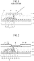
- FIG. 1 is a cross sectional view of a top emission type OLED device according to the related art.
- a thin film transistor layer (T) including an active layer 11, a gate insulating film 12, a gate electrode 13, an insulating interlayer 14, a source electrode 15, and a drain electrode 16 is provided on a substrate 10, and then a passivation layer 20 and a planarization layer 30 are sequentially provided on the thin film transistor layer (T).
- An anode electrode 40 is then provided on the planarization layer 30.
- a bank 50 is provided to define a pixel region.
- an organic emitting layer 60 is provided in the pixel region defined by the bank 50, and a cathode electrode 70 is provided on the organic emitting layer 60.
- the cathode electrode 70 is typically formed of a transparent conductive material.
- the organic emitting layer 60 may be separated from the cathode electrode 70, to thereby lower reliability of the OLED device.
- embodiments of the present invention are directed to an organic light emitting display device and a method of manufacturing the same that substantially obviate one or more problems due to limitations and disadvantages of the related art.
- An aspect of embodiments of the present invention is directed to provide a top emission type organic light emitting display device with enhanced reliability, and a method of manufacturing the same.
- an OLED device may, for example, include a thin film transistor on a substrate; a first electrode electrically connected with the thin film transistor; an organic emitting layer on the first electrode, organic emitting layer separated by a partition; a partition cover on the partition; a second electrode on the organic emitting layer; and an encapsulation layer on the second electrode, wherein a width of an upper surface of the partition cover is smaller than a width of a lower surface of the partition cover.
- a method of manufacturing an OLED device may, for example, include providing a thin film transistor on a substrate; providing a first electrode electrically connected with the thin film transistor, and providing an auxiliary electrode in the same layer as the first electrode; providing a partition on the auxiliary electrode; providing a bank at a lateral side of the first electrode and the auxiliary electrode; providing a partition cover on the partition; providing an organic emitting layer on the first electrode; providing a second electrode on the organic emitting layer; and providing an encapsulation layer on the second electrode, wherein a width of an upper surface of the partition cover is smaller than a width of a lower surface of the partition cover.
- first element at least one among a first element, a second element and a third element
- first element is positioned "on or above” a second element, it should be understood that the first and second elements may be brought into contact with each other, or a third element may be interposed between the first and second elements.
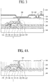
- FIG. 2 is a cross-sectional view illustrating an OLED device according to one embodiment of the present invention.
- the OLED device includes a thin film transistor (T), a passivation layer 200, a planarization layer 250, a first electrode 300, a partition 400, a bank 450, a partition cover 500, an organic emitting layer 550, a second electrode 600 and an encapsulation layer 650 on a substrate 100.
- T thin film transistor
- the thin film transistor (T) may include an active layer 110, a gate insulating film 120, a gate electrode 130, an insulating interlayer 140, a source electrode 150, and a drain electrode 160.
- the active layer 110 is provided on the substrate 100, and is overlapped with the gate electrode 130.
- the active layer 110 may be formed of a silicon-based semiconductor material, or an oxide-based semiconductor material.
- a light-shielding layer may be additionally provided between the substrate 100 and the active layer 110.
- the gate insulating film 120 is disposed on the active layer 110.
- the gate insulating film 120 is provided to insulate the active layer 110 and the gate electrode 130 from each other.
- the gate insulating film 120 may be formed in a single layer of an inorganic insulating material such as silicon oxide (SiOx) or silicon nitride (SiNx), or a multi-layered structure including one or more of silicon oxide (SiOx) and silicon nitride (SiNx), but the embodiment is not limited to these structures.
- the gate electrode 130 is provided on the gate insulating film 120.
- the gate electrode 130 overlaps with the active layer 110, and the gate insulating film 120 is interposed between the gate electrode 130 and the active layer 110 being overlapped with each other.
- the gate electrode 130 may be formed in a single layer or a multi-layered structure including, for example, one or more of molybdenum (Mo), aluminum (Al), chromium (Cr), gold (Au), titanium (Ti), nickel (Ni), neodymium (Nd), copper (Cu) and their alloys, but the embodiment is not limited to these materials.
- the insulating interlayer 140 is provided on the gate electrode 130.
- the insulating interlayer 140 is formed of the same material as the gate insulating film 120.
- the insulating interlayer 140 may be formed in a single layer of an inorganic insulating material such as silicon oxide (SiOx) or silicon nitride (SiNx), or a multi-layered structure including one or more of silicon oxide (SiOx) and silicon nitride (SiNx), but the embodiment is not limited to these materials and structures.
- the source electrode 150 and the drain electrode 160 confronting each other are provided on the insulating interlayer 140.
- a first contact hole (CH1) for exposing one end of the active layer 110 is provided in the aforementioned gate insulating film 120 and the insulating interlayer 140
- a second contact hole (CH2) for exposing the other end of the active layer 110 is provided in the aforementioned gate insulating film 120 and the insulating interlayer 140.
- the source electrode 150 is connected with the other end of the active layer 110 via the first contact hole (CH1)
- the drain electrode 160 is connected with one end of the active layer 110 via the second contact hole (CH2).
- the thin film transistor layer (T) is not limited to the above-described structure, and the thin film transistor layer (T) may be changed to various structures and shapes generally known to those in the art.
- Figure 2 illustrates a top gate structure where the gate electrode 130 is provided on the active layer 110, but it is possible to provide, for example, a bottom gate structure where the gate electrode 130 is provided below the active layer 110.
- the passivation layer 200 is provided on the thin film transistor layer (T) to protect the thin film transistor layer (T).
- the passivation layer 200 may be formed of an inorganic insulating material, for example, silicon oxide film (SiOx) or silicon nitride film (SiNx), but is not limited to these materials.
- the planarization layer 250 is provided on the passivation layer 200 to planarize an upper surface of the substrate 100 with the thin film transistor layer (T).
- the planarization layer 250 may be formed of an organic insulating material, for example, acryl resin, epoxy resin, phenolic resin, polyamide resin, polyimide resin, and etc., but is not limited to these materials.
- the first electrode 300 is disposed on the planarization layer 250.
- a third contact hole (CH3) for exposing the drain electrode 160 is prepared in the passivation layer 200 and the planarization layer 250, and the first electrode 300 is connected with the drain electrode 160 via the third contact hole (CH3). That is, the first electrode 300 is electrically connected with the thin film transistor (T).
- the first electrode 300 is separately disposed in every pixel.
- the first electrode 300 may function as an anode electrode.
- the first electrode 300 may be formed of indium-tin-oxide (ITO) or indium-zinc-oxide (IZO).
- the first electrode 300 may be formed to have a multi-layered structure including metal materials with high reflection efficiency, for example, molybdenum (Mo), alloy (MoTi) of molybdenum (Mo) and titanium (Ti), aluminum (Al), silver (Ag), APC (Ag;Pb;Cu), and etc.
- Mo molybdenum
- MoTi alloy of molybdenum
- Ti titanium
- Al aluminum
- Al aluminum
- APC Ag;Pb;Cu
- metal materials with high reflection efficiency for example, molybdenum (Mo), alloy (MoTi) of molybdenum (Mo) and titanium (Ti), aluminum (Al), silver (Ag), APC (Ag;Pb;Cu), and etc.
- the partition 400 is disposed on the bank 450 to separate the organic emitting layer 550.
- a width of an upper surface of the partition 400 is larger than a width of a lower surface of the partition 400.
- the upper surface of the partition 400 serves as the eaves so that the organic emitting layer 550 is not deposited on an area below the eaves. That is, there may be no need for a mask pattern covering the upper surface of the bank 450. If the gap space is covered by the upper surface of the partition 400 serving as the eaves, it is possible to reduce or prevent the organic emitting layer 550 from being permeated into the gap space.
- the organic emitting layer 550 can be manufactured by a deposition process using a deposition material with superior straightness, the organic emitting layer 550 may not be deposited in the gap space during the deposition process.
- the partition 400 may be formed of a photo-sensitive material whose portion exposed to light is cured.
- the bank 450 is provided on the first electrode 300.
- the bank 450 is partially overlapped with the first electrode 300. That is, the bank 450, which exposes the upper surface of the first electrode 300, is provided on one side and the other side of the first electrode 300 so as to cover a lateral surface of the first electrode 300.
- the bank 450 may be formed of an organic insulating material, for example, polyimide resin, acryl resin, benzocyclobutene BCB, and etc., but is not limited to these materials.
- the partition cover 500 is disposed on the partition 400.
- the partition cover 500 and the bank 450 may be formed of the same material and at the same time.
- a width of an upper surface of the partition cover 500 is smaller than a width of a lower surface of the partition cover 500.
- the upper surface of the partition cover 500 serves as a supporter of the mask, so that it is possible to reduce or prevent the supporter from being in contact with the upper surface of the partition 400.
- the partition cover 500 is not provided on the partition 400, and thus, the mask for depositing the organic emitting layer 550 may be in contact with the upper surface of the partition 400. If the mask is in contact with the partition 400 with the upper surface having a relatively-large width, the mask may be contaminated by foreign matters of the partition 400. Also, the first electrode 300 may be contaminated by the foreign matters during a process of transferring the mask.
- the partition cover 500 with the upper surface having a relatively-small width is disposed on the partition 400 so that it is possible to reduce or minimize a contact area with the mask, and furthermore, to reduce or prevent defects caused by the foreign matters of the mask.
- the organic emitting layer 550 is disposed on the first electrode 300.
- the organic emitting layer 550 may include a hole injecting layer, a hole transporting layer, an emitting layer, an electron transporting layer, and an electron injecting layer.
- a structure of the organic emitting layer 550 may be changed to various shapes generally known to those in the art.
- the organic emitting layer 550 may extend to the upper surface of the bank 450. However, when the organic emitting layer 550 extends to the upper surface of the bank 450, the organic emitting layer 550 is not formed in the gap space prepared between the lower surface of the partition 400 and the bank 450 by the partition 400.
- the second electrode 600 is provided on the organic emitting layer 550.
- the second electrode 600 functions as a cathode electrode.
- the second electrode 600 is formed of a transparent conductive material.
- the second electrode 600 is not formed in the gap space prepared between the lower surface of the partition 400 and the bank 450 by the partition 400. If the second electrode 600 is manufactured by a sputtering process using a deposition material with less straightness, the second electrode 600 may be deposited in the gap space during the deposition process.
- the encapsulation layer 650 for preventing a permeation of moisture may be entirely provided on the second electrode 600.
- the encapsulation layer 650 may be formed of various materials generally known to those in the art.
- the encapsulation layer 650 may be prepared in the gap space between the partition 400 and the bank 450. That is, the encapsulation layer 650 is prepared in the gap space, and is disposed while being inserted into the space between the lower surface of the partition 400 and the bank 450, whereby the encapsulation layer 650 is not separated from the second electrode 600. Also, the encapsulation layer 650 is provided in the gap space so that it is possible to fixedly provide the second electrode 600 and the organic emitting layer 550 without separation.
- the partition 400 is disposed in-between the organic emitting layer 550 and also disposed in-between the second electrode 600, and the encapsulation layer 650 is provided in the space between the partition 400 and the bank 450, to thereby fixedly provide the encapsulation layer 650.
- the encapsulation layer 650 of the OLED device according to one embodiment of the present invention presses the organic emitting layer 550 and the second electrode 600, to thereby enhance an adhesive strength between the organic emitting layer 550 and the second electrode 600. Accordingly, even when an impact is applied by repetitive bending actions, it is possible to reduce or prevent the organic emitting layer 550 from being separated from the cathode electrode 600, to thereby improve reliability.
- FIG. 3 is a cross-sectional view illustrating an OLED device according to another embodiment of the present invention. Except an auxiliary electrode, a partition, and a bank, the OLED device of FIG. 3 is the same as the OLED device of FIG. 2 .
- the auxiliary electrode, partition, and bank will be described in detail, and a detailed description for the same parts will be omitted.
- An auxiliary electrode 350 is disposed on a planarization layer 250. That is, the auxiliary electrode 350 is disposed in the same layer as a first electrode 300. In order to reduce a resistance of a second electrode 600, the auxiliary electrode 350 is electrically connected with the second electrode 600. The auxiliary electrode 350 is connected with the second electrode 600 through an area without the bank 450, and an area exposed to a lower side of a partition 400.
- the partition 400 is disposed on the auxiliary electrode 350, wherein the partition 400 is provided to separate an organic emitting layer 550.
- a width of an upper surface of the partition 400 is larger than a width of a lower surface of the partition 400.
- the upper surface of the partition 400 serves as the eaves so that the organic emitting layer 550 is not deposited on an area below the eaves. That is, there may be no need for a mask pattern covering the upper surface of the auxiliary electrode 350.
- the gap space is covered by the upper surface of the partition 400 serving as the eaves, it is possible to reduce or prevent the organic emitting layer 550 from being permeated into the gap space. Since the organic emitting layer 550 is manufactured by a deposition process using a deposition material with superior straightness, the organic emitting layer 550 is not deposited in the gap space between the partition 400 and the auxiliary electrode 350 during the deposition process.
- the partition 400 may be formed of a photo-sensitive material whose portion exposed to light is cured.
- the bank 450 is disposed on the first electrode 300 and the auxiliary electrode 350.
- the bank 450 is partially overlapped with the first electrode 300 and the auxiliary electrode 350. That is, the bank 450, which exposes the upper surface of the first electrode 300 and the auxiliary electrode 350, is provided on one side and the other side of the first electrode 300 and the auxiliary electrode 350 so as to cover the lateral surface of the first electrode 300 and the auxiliary electrode 350.
- the bank 450 is provided to expose the upper surface of the first electrode 300, it is possible to secure an image-displaying area.
- the bank 450 is provided to expose the upper surface of the auxiliary electrode 350, it is possible to secure an electrical connection space between the auxiliary electrode 350 and the second electrode 600.
- the bank 450 is disposed between the first electrode 300 and the auxiliary electrode 350, to thereby electrically insulate the first electrode 300 and the auxiliary electrode 350 from each other.
- the bank 450 may be formed of an organic insulating material, for example, polyimide resin, acryl resin, benzocyclobutene BCB, and etc., but is not limited to these materials.
- the partition 400 is disposed on the auxiliary electrode 350, and the auxiliary electrode 350 is exposed to and connected with the second electrode 600 without using a mask pattern.
- a partition cover 500 is disposed on the partition 400, wherein a width of an upper surface of the partition cover 500 is relatively small, so that it is possible to reduce or minimize a contact area with the mask, to reduce or prevent the mask from being contaminated by foreign matters, and thus, to reduce or prevents defects caused by the foreign matters of the mask.
- the partition 400 is disposed in-between the organic emitting layer 550 to separate the organic emitting layer 550, and also disposed in-between the second electrode 600 to separate the second electrode 600, and an encapsulation layer 650 is provided in the space between the partition 400 and the bank 450, to thereby fixedly provide the encapsulation layer 650.
- the encapsulation layer 650 presses the organic emitting layer 550 and the second electrode 600, to thereby enhance an adhesive strength between the organic emitting layer 550 and the second electrode 600. Accordingly, even when an impact is applied by repetitive bending actions, it is possible to reduce or prevent the organic emitting layer 550 from being separated from the cathode electrode 600, to thereby improve reliability.
- FIGs. 4A to 4F are cross-sectional views illustrating a method of manufacturing an OLED device according to another embodiment of the present invention, as applied to the OLED device illustrated in FIG. 3 .
- the same reference numbers will be used throughout the drawings to refer to the same or like parts, and a repetitive explanation for the material and structure of each of the elements will be omitted.
- the thin film transistor (T) is formed on the substrate 100, the passivation layer 200 is provided on the thin film transistor (T), and the planarization layer 250 is provided on the passivation layer 200.
- the process of forming the thin film transistor (T) may include providing the active layer 110 on the substrate 100, providing the gate insulating film 120 on the active layer 110, providing the gate electrode 130 on the gate insulating film 120, providing the insulating interlayer 140 on the gate electrode 130, providing the first and second contact holes (CH1, CH2) in the insulating interlayer 140 and the gate insulating film 120, and providing the source and drain electrodes 150 and 160 on the insulating interlayer 140 and connecting the source and drain electrodes 150 and 160 with the active layer 110 via the first and second contact holes (CH1, CH2).
- various methods generally known to those in the art can be applied to form the thin film transistor (T).
- the third contact hole (CH3) for exposing the drain electrode 160 of the thin film transistor (T) is provided in the passivation layer 200 and the planarization layer 250, and then the first electrode 300 is electrically connected with the drain electrode 160 via the third contact hole (CH3).
- the process of providing the first electrode 300 on the planarization layer 250 and the process of the auxiliary electrode 350 on the planarization layer 250 may be carried out at the same time. That is, the first electrode 300 and the auxiliary electrode 350 may be simultaneously manufactured on the same layer, that is, the planarization layer 250.
- the partition 400 is provided on the auxiliary electrode 350.
- the partition 400 is formed of the photo-sensitive material whose portion exposed to light is cured, which may be formed of negative type photoresist (PR).
- PR negative type photoresist
- a portion exposed to light remains by a chemical combination, and another portion which is not exposed to light is removed by a developing solution. Accordingly, under the condition that a partition material is deposited on the auxiliary electrode 350, and that the mask is disposed above the partition material, light is irradiated thereon, whereby the partition material covered by the mask is removed, and the partition material exposed to light remains to be the partition 400.
- the lower surface of the partition 400 may be formed in a reverse-tapered shape. Accordingly, the width of the upper surface of the partition 400 is larger than the width of the lower surface of the partition 400.
- the bank 450 is provided at a lateral side of the first electrode 300 and the auxiliary electrode 350, and the partition cover 500 is provided on the partition 400.
- the process of providing the partition cover 500 on the partition 400 and the process of providing the bank 450 at the lateral side of the first electrode 300 and the auxiliary electrode 350 may be carried out at the same time.
- the partition cover 500 and the bank 450 may be formed of the same material. In this case, the width of the upper surface of the partition cover 500 is smaller than the width of the lower surface of the partition cover 500.
- the bank 450 is laterally irradiated with light, whereby the bank 450 is removed from the space between the partition 400 and the auxiliary electrode 350.
- the gap space between the lower surface of the partition 400 and the auxiliary electrode 350 whereby the second electrode 600 and the encapsulation layer 650 may be prepared in the gap space for the following process.
- a mask is disposed above the partition cover 500.
- the organic emitting layer 550 is provided on the first electrode 300.
- the organic emitting layer 550 may be provided on an entire surface of the substrate 100, and then the second electrode 600 may be provided on the organic emitting layer 550.
- the encapsulation layer 650 is provided on the second electrode 600. At this time, the encapsulation layer 650 may be provided in the space between the partition 400 and the auxiliary electrode 350 and the space between the partition 400 and the bank 450.
- the partition cover 500 is disposed on the partition 400, wherein the width of the upper surface of the partition cover 500 is relatively small, so that it is possible to reduce or minimize a contact area with the mask, to reduce or prevent the mask from being contaminated by foreign matters, and to thereby reduce or prevent defects caused by the foreign matters of the mask.
- the bank 450 and the partition cover 500 for preventing the mask from being contaminated by foreign matters are manufactured at the same time so that the partition cover 500 is provided on the partition 400 without increasing the number of masks, to thereby improve reliability of the OLED device.
- the partition cover 500 with the upper surface having a relatively-small width is disposed on the partition 400 so that it is possible to reduce or minimize the contact area with the mask, to reduce or prevent the mask from being contaminated by foreign matters, and to thereby reduce or prevent defects caused by the foreign matters of the mask.
- the bank 450 and the partition cover 500 for preventing the mask from being contaminated by foreign matters are manufactured at the same time so that the partition cover 500 is provided on the partition 400 without increasing the number of masks, to thereby improve reliability of the OLED device.
- the adhesive strength between the organic emitting layer 550 and the second electrode 600 is improved by the partition 400 so that it is possible to reduce or prevent separation between the organic emitting layer 550 and the cathode electrode, thereby improving reliability of the OLED device.
Landscapes
- Engineering & Computer Science (AREA)
- Physics & Mathematics (AREA)
- General Engineering & Computer Science (AREA)
- General Physics & Mathematics (AREA)
- Microelectronics & Electronic Packaging (AREA)
- Optics & Photonics (AREA)
- Manufacturing & Machinery (AREA)
- Theoretical Computer Science (AREA)
- Computer Networks & Wireless Communication (AREA)
- Quality & Reliability (AREA)
- Computer Hardware Design (AREA)
- Geometry (AREA)
- Electroluminescent Light Sources (AREA)
Abstract
Description
- Embodiments of the present invention relate to an organic light emitting display device, and more particularly, to a top emission type organic light emitting display device.
- An organic light emitting display (OLED) device, which is a self light emitting display device, has advantages of low power consumption, rapid response speed, high emission efficiency, high luminance and wide viewing angle.
- According to a direction of the light emitted from an OLED device, the OLED device may be largely classified into a top emission type and a bottom emission type. In case of the bottom emission type, a circuit device is disposed between a light emitting layer and an image displaying surface, which may lower aperture ratio due to the circuit device. Meanwhile, in case of the top emission type, a circuit device is typically not disposed between a light emitting layer and an image displaying surface and thus, is more advantageous from an aperture ratio standpoint.
-
FIG. 1 is a cross sectional view of a top emission type OLED device according to the related art. - As shown in
FIG. 1 , a thin film transistor layer (T) including anactive layer 11, agate insulating film 12, agate electrode 13, aninsulating interlayer 14, asource electrode 15, and adrain electrode 16 is provided on asubstrate 10, and then apassivation layer 20 and aplanarization layer 30 are sequentially provided on the thin film transistor layer (T). - An
anode electrode 40 is then provided on theplanarization layer 30. On theanode electrode 40, a bank 50 is provided to define a pixel region. Also, anorganic emitting layer 60 is provided in the pixel region defined by the bank 50, and acathode electrode 70 is provided on theorganic emitting layer 60. - In case of the top emission type, the light emitted from the
organic emitting layer 60 passes through thecathode electrode 70. To do so, thecathode electrode 70 is typically formed of a transparent conductive material. - However, when the OLED device according the related art is subject to impact by repetitive bending actions, the
organic emitting layer 60 may be separated from thecathode electrode 70, to thereby lower reliability of the OLED device. - Accordingly, embodiments of the present invention are directed to an organic light emitting display device and a method of manufacturing the same that substantially obviate one or more problems due to limitations and disadvantages of the related art.
- An aspect of embodiments of the present invention is directed to provide a top emission type organic light emitting display device with enhanced reliability, and a method of manufacturing the same.
- Additional features and advantages of the present invention will be set forth in the description which follows, and in part will be apparent from the description, or may be learned by practice of the invention. These and other advantages of the present invention will be realized and attained by the structure particularly pointed out in the written description and claims hereof as well as the appended drawings.
- To achieve these and other advantages and in accordance with the purpose of embodiments of the invention, as embodied and broadly described herein, an OLED device may, for example, include a thin film transistor on a substrate; a first electrode electrically connected with the thin film transistor; an organic emitting layer on the first electrode, organic emitting layer separated by a partition; a partition cover on the partition; a second electrode on the organic emitting layer; and an encapsulation layer on the second electrode, wherein a width of an upper surface of the partition cover is smaller than a width of a lower surface of the partition cover.
- In another aspect, a method of manufacturing an OLED device may, for example, include providing a thin film transistor on a substrate; providing a first electrode electrically connected with the thin film transistor, and providing an auxiliary electrode in the same layer as the first electrode; providing a partition on the auxiliary electrode; providing a bank at a lateral side of the first electrode and the auxiliary electrode; providing a partition cover on the partition; providing an organic emitting layer on the first electrode; providing a second electrode on the organic emitting layer; and providing an encapsulation layer on the second electrode, wherein a width of an upper surface of the partition cover is smaller than a width of a lower surface of the partition cover.
- It is to be understood that both the foregoing general description and the following detailed description are exemplary and explanatory and are intended to provide further explanation of the invention as claimed.
- The accompanying drawings, which are included to provide a further understanding of embodiments of the invention and are incorporated in and constitute a part of this application, illustrate embodiment(s) of the invention and together with the description serve to explain the principle of embodiments of the invention. In the drawings:
-
FIG. 1 is a cross-sectional view illustrating a top emission type OLED device according to the related art; -
FIG. 2 is a cross-sectional view illustrating an OLED device according to one embodiment of the present invention; -
FIG. 3 is a cross-sectional view illustrating an OLED device according to another embodiment of the present invention; and -
FIGs. 4A to 4F are cross-sectional views illustrating a method of manufacturing the OLED device according to another embodiment of the present invention. - Terms disclosed in this specification should be understood as follows. The term of a singular expression should be understood to include a multiple expression as well as the singular expression if there is no specific definition in the context. The terms such as "the first" and "the second" are used only to differentiate one element from other elements. Thus, a scope of claims is not limited by these terms. Also, it should be understood that the term such as "include" or "have" does not preclude existence or possibility of one or more features, numbers, steps, operations, elements, parts or their combinations. It should be understood that the term "at least one" includes all combinations related with any one item. For example, "at least one among a first element, a second element and a third element" may include all combinations of two or more elements selected from the first, second and third elements as well as each element of the first, second and third elements. Also, if it is mentioned that a first element is positioned "on or above" a second element, it should be understood that the first and second elements may be brought into contact with each other, or a third element may be interposed between the first and second elements.
- Hereinafter, reference will now be made in detail to embodiments of the present disclosure, examples of which are illustrated in the accompanying drawings. Wherever possible, the same reference numbers will be used throughout the drawings to refer to the same or like parts. Also, in the following description of the present disclosure, if detailed description of elements or functions known is determined to make the subject matter of the present disclosure unnecessarily obscure, the detailed description thereof will be omitted.
-
FIG. 2 is a cross-sectional view illustrating an OLED device according to one embodiment of the present invention. - Referring to
FIG. 2 , the OLED device includes a thin film transistor (T), apassivation layer 200, aplanarization layer 250, afirst electrode 300, apartition 400, abank 450, apartition cover 500, anorganic emitting layer 550, asecond electrode 600 and anencapsulation layer 650 on asubstrate 100. - The thin film transistor (T) may include an
active layer 110, agate insulating film 120, agate electrode 130, aninsulating interlayer 140, asource electrode 150, and adrain electrode 160. - The
active layer 110 is provided on thesubstrate 100, and is overlapped with thegate electrode 130. Theactive layer 110 may be formed of a silicon-based semiconductor material, or an oxide-based semiconductor material. Although not shown, a light-shielding layer may be additionally provided between thesubstrate 100 and theactive layer 110. - The
gate insulating film 120 is disposed on theactive layer 110. Thegate insulating film 120 is provided to insulate theactive layer 110 and thegate electrode 130 from each other. In this case, the gateinsulating film 120 may be formed in a single layer of an inorganic insulating material such as silicon oxide (SiOx) or silicon nitride (SiNx), or a multi-layered structure including one or more of silicon oxide (SiOx) and silicon nitride (SiNx), but the embodiment is not limited to these structures. - The
gate electrode 130 is provided on thegate insulating film 120. Thegate electrode 130 overlaps with theactive layer 110, and thegate insulating film 120 is interposed between thegate electrode 130 and theactive layer 110 being overlapped with each other. Thegate electrode 130 may be formed in a single layer or a multi-layered structure including, for example, one or more of molybdenum (Mo), aluminum (Al), chromium (Cr), gold (Au), titanium (Ti), nickel (Ni), neodymium (Nd), copper (Cu) and their alloys, but the embodiment is not limited to these materials. - The
insulating interlayer 140 is provided on thegate electrode 130. Theinsulating interlayer 140 is formed of the same material as thegate insulating film 120. For example, theinsulating interlayer 140 may be formed in a single layer of an inorganic insulating material such as silicon oxide (SiOx) or silicon nitride (SiNx), or a multi-layered structure including one or more of silicon oxide (SiOx) and silicon nitride (SiNx), but the embodiment is not limited to these materials and structures. - The
source electrode 150 and thedrain electrode 160 confronting each other are provided on theinsulating interlayer 140. A first contact hole (CH1) for exposing one end of theactive layer 110 is provided in the aforementionedgate insulating film 120 and theinsulating interlayer 140, and a second contact hole (CH2) for exposing the other end of theactive layer 110 is provided in the aforementionedgate insulating film 120 and theinsulating interlayer 140. Thesource electrode 150 is connected with the other end of theactive layer 110 via the first contact hole (CH1), and thedrain electrode 160 is connected with one end of theactive layer 110 via the second contact hole (CH2). - The thin film transistor layer (T) is not limited to the above-described structure, and the thin film transistor layer (T) may be changed to various structures and shapes generally known to those in the art. For example,
Figure 2 illustrates a top gate structure where thegate electrode 130 is provided on theactive layer 110, but it is possible to provide, for example, a bottom gate structure where thegate electrode 130 is provided below theactive layer 110. - The
passivation layer 200 is provided on the thin film transistor layer (T) to protect the thin film transistor layer (T). Thepassivation layer 200 may be formed of an inorganic insulating material, for example, silicon oxide film (SiOx) or silicon nitride film (SiNx), but is not limited to these materials. - The
planarization layer 250 is provided on thepassivation layer 200 to planarize an upper surface of thesubstrate 100 with the thin film transistor layer (T). Theplanarization layer 250 may be formed of an organic insulating material, for example, acryl resin, epoxy resin, phenolic resin, polyamide resin, polyimide resin, and etc., but is not limited to these materials. - The
first electrode 300 is disposed on theplanarization layer 250. A third contact hole (CH3) for exposing thedrain electrode 160 is prepared in thepassivation layer 200 and theplanarization layer 250, and thefirst electrode 300 is connected with thedrain electrode 160 via the third contact hole (CH3). That is, thefirst electrode 300 is electrically connected with the thin film transistor (T). In this case, thefirst electrode 300 is separately disposed in every pixel. For example, thefirst electrode 300 may function as an anode electrode. Thefirst electrode 300 may be formed of indium-tin-oxide (ITO) or indium-zinc-oxide (IZO). Also, thefirst electrode 300 may be formed to have a multi-layered structure including metal materials with high reflection efficiency, for example, molybdenum (Mo), alloy (MoTi) of molybdenum (Mo) and titanium (Ti), aluminum (Al), silver (Ag), APC (Ag;Pb;Cu), and etc. - The
partition 400 is disposed on thebank 450 to separate the organic emittinglayer 550. In order to provide thepartition 400 whose upper surface serves as eaves, a width of an upper surface of thepartition 400 is larger than a width of a lower surface of thepartition 400. During a process of depositing the organic emittinglayer 550, the upper surface of thepartition 400 serves as the eaves so that the organic emittinglayer 550 is not deposited on an area below the eaves. That is, there may be no need for a mask pattern covering the upper surface of thebank 450. If the gap space is covered by the upper surface of thepartition 400 serving as the eaves, it is possible to reduce or prevent the organic emittinglayer 550 from being permeated into the gap space. Since the organic emittinglayer 550 can be manufactured by a deposition process using a deposition material with superior straightness, the organic emittinglayer 550 may not be deposited in the gap space during the deposition process. Thepartition 400 may be formed of a photo-sensitive material whose portion exposed to light is cured. - The
bank 450 is provided on thefirst electrode 300. Thebank 450 is partially overlapped with thefirst electrode 300. That is, thebank 450, which exposes the upper surface of thefirst electrode 300, is provided on one side and the other side of thefirst electrode 300 so as to cover a lateral surface of thefirst electrode 300. As thebank 450 is provided to expose the upper surface of thefirst electrode 300, it is possible to secure an image-displaying area. Thebank 450 may be formed of an organic insulating material, for example, polyimide resin, acryl resin, benzocyclobutene BCB, and etc., but is not limited to these materials. - The
partition cover 500 is disposed on thepartition 400. Thepartition cover 500 and thebank 450 may be formed of the same material and at the same time. In order to reduce a contact with a mask for a manufacturing process, a width of an upper surface of thepartition cover 500 is smaller than a width of a lower surface of thepartition cover 500. During a deposition process of the organic emittinglayer 550, the upper surface of thepartition cover 500 serves as a supporter of the mask, so that it is possible to reduce or prevent the supporter from being in contact with the upper surface of thepartition 400. - In case of the related art OLED device, the
partition cover 500 is not provided on thepartition 400, and thus, the mask for depositing the organic emittinglayer 550 may be in contact with the upper surface of thepartition 400. If the mask is in contact with thepartition 400 with the upper surface having a relatively-large width, the mask may be contaminated by foreign matters of thepartition 400. Also, thefirst electrode 300 may be contaminated by the foreign matters during a process of transferring the mask. In the OLED device according to one embodiment of the present disclosure, thepartition cover 500 with the upper surface having a relatively-small width is disposed on thepartition 400 so that it is possible to reduce or minimize a contact area with the mask, and furthermore, to reduce or prevent defects caused by the foreign matters of the mask. - The organic emitting
layer 550 is disposed on thefirst electrode 300. The organic emittinglayer 550 may include a hole injecting layer, a hole transporting layer, an emitting layer, an electron transporting layer, and an electron injecting layer. A structure of the organic emittinglayer 550 may be changed to various shapes generally known to those in the art. The organic emittinglayer 550 may extend to the upper surface of thebank 450. However, when the organic emittinglayer 550 extends to the upper surface of thebank 450, the organic emittinglayer 550 is not formed in the gap space prepared between the lower surface of thepartition 400 and thebank 450 by thepartition 400. - The
second electrode 600 is provided on the organic emittinglayer 550. In this case, if thefirst electrode 300 functions as an anode electrode, thesecond electrode 600 functions as a cathode electrode. As thesecond electrode 600 is provided on a surface from which light is emitted, thesecond electrode 600 is formed of a transparent conductive material. In the same manner as the organic emittinglayer 550, thesecond electrode 600 is not formed in the gap space prepared between the lower surface of thepartition 400 and thebank 450 by thepartition 400. If thesecond electrode 600 is manufactured by a sputtering process using a deposition material with less straightness, thesecond electrode 600 may be deposited in the gap space during the deposition process. - The
encapsulation layer 650 for preventing a permeation of moisture may be entirely provided on thesecond electrode 600. Theencapsulation layer 650 may be formed of various materials generally known to those in the art. Theencapsulation layer 650 may be prepared in the gap space between thepartition 400 and thebank 450. That is, theencapsulation layer 650 is prepared in the gap space, and is disposed while being inserted into the space between the lower surface of thepartition 400 and thebank 450, whereby theencapsulation layer 650 is not separated from thesecond electrode 600. Also, theencapsulation layer 650 is provided in the gap space so that it is possible to fixedly provide thesecond electrode 600 and the organic emittinglayer 550 without separation. - In the OLED device according to one embodiment of the present invention, the
partition 400 is disposed in-between the organic emittinglayer 550 and also disposed in-between thesecond electrode 600, and theencapsulation layer 650 is provided in the space between thepartition 400 and thebank 450, to thereby fixedly provide theencapsulation layer 650. Accordingly, theencapsulation layer 650 of the OLED device according to one embodiment of the present invention presses the organic emittinglayer 550 and thesecond electrode 600, to thereby enhance an adhesive strength between the organic emittinglayer 550 and thesecond electrode 600. Accordingly, even when an impact is applied by repetitive bending actions, it is possible to reduce or prevent the organic emittinglayer 550 from being separated from thecathode electrode 600, to thereby improve reliability. -
FIG. 3 is a cross-sectional view illustrating an OLED device according to another embodiment of the present invention. Except an auxiliary electrode, a partition, and a bank, the OLED device ofFIG. 3 is the same as the OLED device ofFIG. 2 . Hereinafter, the auxiliary electrode, partition, and bank will be described in detail, and a detailed description for the same parts will be omitted. - An
auxiliary electrode 350 is disposed on aplanarization layer 250. That is, theauxiliary electrode 350 is disposed in the same layer as afirst electrode 300. In order to reduce a resistance of asecond electrode 600, theauxiliary electrode 350 is electrically connected with thesecond electrode 600. Theauxiliary electrode 350 is connected with thesecond electrode 600 through an area without thebank 450, and an area exposed to a lower side of apartition 400. - The
partition 400 is disposed on theauxiliary electrode 350, wherein thepartition 400 is provided to separate an organic emittinglayer 550. In order to provide thepartition 400 whose upper surface serves as eaves, a width of an upper surface of thepartition 400 is larger than a width of a lower surface of thepartition 400. During a process of depositing the organic emittinglayer 550, the upper surface of thepartition 400 serves as the eaves so that the organic emittinglayer 550 is not deposited on an area below the eaves. That is, there may be no need for a mask pattern covering the upper surface of theauxiliary electrode 350. If the gap space is covered by the upper surface of thepartition 400 serving as the eaves, it is possible to reduce or prevent the organic emittinglayer 550 from being permeated into the gap space. Since the organic emittinglayer 550 is manufactured by a deposition process using a deposition material with superior straightness, the organic emittinglayer 550 is not deposited in the gap space between thepartition 400 and theauxiliary electrode 350 during the deposition process. Thepartition 400 may be formed of a photo-sensitive material whose portion exposed to light is cured. - The
bank 450 is disposed on thefirst electrode 300 and theauxiliary electrode 350. Thebank 450 is partially overlapped with thefirst electrode 300 and theauxiliary electrode 350. That is, thebank 450, which exposes the upper surface of thefirst electrode 300 and theauxiliary electrode 350, is provided on one side and the other side of thefirst electrode 300 and theauxiliary electrode 350 so as to cover the lateral surface of thefirst electrode 300 and theauxiliary electrode 350. According as thebank 450 is provided to expose the upper surface of thefirst electrode 300, it is possible to secure an image-displaying area. Also, as thebank 450 is provided to expose the upper surface of theauxiliary electrode 350, it is possible to secure an electrical connection space between theauxiliary electrode 350 and thesecond electrode 600. Thebank 450 is disposed between thefirst electrode 300 and theauxiliary electrode 350, to thereby electrically insulate thefirst electrode 300 and theauxiliary electrode 350 from each other. Thebank 450 may be formed of an organic insulating material, for example, polyimide resin, acryl resin, benzocyclobutene BCB, and etc., but is not limited to these materials. - In the OLED device according to another embodiment of the present invention, the
partition 400 is disposed on theauxiliary electrode 350, and theauxiliary electrode 350 is exposed to and connected with thesecond electrode 600 without using a mask pattern. Apartition cover 500 is disposed on thepartition 400, wherein a width of an upper surface of thepartition cover 500 is relatively small, so that it is possible to reduce or minimize a contact area with the mask, to reduce or prevent the mask from being contaminated by foreign matters, and thus, to reduce or prevents defects caused by the foreign matters of the mask. - Also, in the OLED device according to another embodiment of the present invention, the
partition 400 is disposed in-between the organic emittinglayer 550 to separate the organic emittinglayer 550, and also disposed in-between thesecond electrode 600 to separate thesecond electrode 600, and anencapsulation layer 650 is provided in the space between thepartition 400 and thebank 450, to thereby fixedly provide theencapsulation layer 650. Theencapsulation layer 650 presses the organic emittinglayer 550 and thesecond electrode 600, to thereby enhance an adhesive strength between the organic emittinglayer 550 and thesecond electrode 600. Accordingly, even when an impact is applied by repetitive bending actions, it is possible to reduce or prevent the organic emittinglayer 550 from being separated from thecathode electrode 600, to thereby improve reliability. -
FIGs. 4A to 4F are cross-sectional views illustrating a method of manufacturing an OLED device according to another embodiment of the present invention, as applied to the OLED device illustrated inFIG. 3 . Thus, the same reference numbers will be used throughout the drawings to refer to the same or like parts, and a repetitive explanation for the material and structure of each of the elements will be omitted. - First, as illustrated in
FIG. 4A , the thin film transistor (T) is formed on thesubstrate 100, thepassivation layer 200 is provided on the thin film transistor (T), and theplanarization layer 250 is provided on thepassivation layer 200. - The process of forming the thin film transistor (T) may include providing the
active layer 110 on thesubstrate 100, providing thegate insulating film 120 on theactive layer 110, providing thegate electrode 130 on thegate insulating film 120, providing the insulatinginterlayer 140 on thegate electrode 130, providing the first and second contact holes (CH1, CH2) in the insulatinginterlayer 140 and thegate insulating film 120, and providing the source and drainelectrodes interlayer 140 and connecting the source and drainelectrodes active layer 110 via the first and second contact holes (CH1, CH2). However, it should be appreciated that various methods generally known to those in the art can be applied to form the thin film transistor (T). - After providing the
passivation layer 200 and theplanarization layer 250, the third contact hole (CH3) for exposing thedrain electrode 160 of the thin film transistor (T) is provided in thepassivation layer 200 and theplanarization layer 250, and then thefirst electrode 300 is electrically connected with thedrain electrode 160 via the third contact hole (CH3). - The process of providing the
first electrode 300 on theplanarization layer 250 and the process of theauxiliary electrode 350 on theplanarization layer 250 may be carried out at the same time. That is, thefirst electrode 300 and theauxiliary electrode 350 may be simultaneously manufactured on the same layer, that is, theplanarization layer 250. - Then, as illustrated in
FIG. 4B , thepartition 400 is provided on theauxiliary electrode 350. Thepartition 400 is formed of the photo-sensitive material whose portion exposed to light is cured, which may be formed of negative type photoresist (PR). In case of a negative photoresist process, a portion exposed to light remains by a chemical combination, and another portion which is not exposed to light is removed by a developing solution. Accordingly, under the condition that a partition material is deposited on theauxiliary electrode 350, and that the mask is disposed above the partition material, light is irradiated thereon, whereby the partition material covered by the mask is removed, and the partition material exposed to light remains to be thepartition 400. At this time, if the partition material is laterally irradiated with light, the lower surface of thepartition 400 may be formed in a reverse-tapered shape. Accordingly, the width of the upper surface of thepartition 400 is larger than the width of the lower surface of thepartition 400. - Then, as illustrated in
FIG. 4C , thebank 450 is provided at a lateral side of thefirst electrode 300 and theauxiliary electrode 350, and thepartition cover 500 is provided on thepartition 400. - The process of providing the
partition cover 500 on thepartition 400 and the process of providing thebank 450 at the lateral side of thefirst electrode 300 and theauxiliary electrode 350 may be carried out at the same time. Thepartition cover 500 and thebank 450 may be formed of the same material. In this case, the width of the upper surface of thepartition cover 500 is smaller than the width of the lower surface of thepartition cover 500. - Then, the
bank 450 is laterally irradiated with light, whereby thebank 450 is removed from the space between thepartition 400 and theauxiliary electrode 350. Thus, it is possible to prepare the gap space between the lower surface of thepartition 400 and theauxiliary electrode 350, whereby thesecond electrode 600 and theencapsulation layer 650 may be prepared in the gap space for the following process. - As illustrated in
FIG. 4D , a mask is disposed above thepartition cover 500. As illustrated inFIG. 4E , the organic emittinglayer 550 is provided on thefirst electrode 300. The organic emittinglayer 550 may be provided on an entire surface of thesubstrate 100, and then thesecond electrode 600 may be provided on the organic emittinglayer 550. - As illustrated in
FIG. 4F , theencapsulation layer 650 is provided on thesecond electrode 600. At this time, theencapsulation layer 650 may be provided in the space between thepartition 400 and theauxiliary electrode 350 and the space between thepartition 400 and thebank 450. - In the OLED device according to another embodiment of the present invention, the
partition cover 500 is disposed on thepartition 400, wherein the width of the upper surface of thepartition cover 500 is relatively small, so that it is possible to reduce or minimize a contact area with the mask, to reduce or prevent the mask from being contaminated by foreign matters, and to thereby reduce or prevent defects caused by the foreign matters of the mask. Also, in the method of manufacturing the OLED device according to another embodiment of the present invention, thebank 450 and thepartition cover 500 for preventing the mask from being contaminated by foreign matters are manufactured at the same time so that thepartition cover 500 is provided on thepartition 400 without increasing the number of masks, to thereby improve reliability of the OLED device. - According to the embodiment of the present invention, the
partition cover 500 with the upper surface having a relatively-small width is disposed on thepartition 400 so that it is possible to reduce or minimize the contact area with the mask, to reduce or prevent the mask from being contaminated by foreign matters, and to thereby reduce or prevent defects caused by the foreign matters of the mask. - Also, the
bank 450 and thepartition cover 500 for preventing the mask from being contaminated by foreign matters are manufactured at the same time so that thepartition cover 500 is provided on thepartition 400 without increasing the number of masks, to thereby improve reliability of the OLED device. - Also, the adhesive strength between the organic emitting
layer 550 and thesecond electrode 600 is improved by thepartition 400 so that it is possible to reduce or prevent separation between the organic emittinglayer 550 and the cathode electrode, thereby improving reliability of the OLED device. - It will be apparent to those skilled in the art that various modifications and variations can be made in the present invention without departing from the scope of the inventions. Thus, it is intended that the present invention covers the modifications and variations of this invention provided they come within the scope of the appended claims and their equivalents.
Claims (12)
- An organic light emitting display (OLED) device comprising:a thin film transistor on a substrate;a first electrode electrically connected with the thin film transistor;an organic emitting layer on the first electrode, the organic emitting layer separated by a partition;a partition cover on the partition;a second electrode on the organic emitting layer; andan encapsulation layer on the second electrode,wherein a width of an upper surface of the partition cover is smaller than a width of a lower surface of the partition cover.
- The OLED device according to claim 1, further comprising an auxiliary electrode disposed in the same layer as the first electrode, wherein the partition is disposed on the auxiliary electrode.
- The OLED device according to claim 2, wherein the second electrode is electrically connected with the auxiliary electrode.
- The OLED device according to any preceding claim, wherein a width of an upper surface of the partition is larger than a width of a lower surface of the partition.
- The OLED device according to any preceding claim, further comprising a bank at a lateral side of the first electrode, wherein the bank and the partition cover are formed of the same material.
- The OLED device according to claim 5, wherein the encapsulation layer is provided in a space between the partition and the bank.
- A method of manufacturing an OLED device comprising:providing a thin film transistor on a substrate;providing a first electrode electrically connected with the thin film transistor, and providing an auxiliary electrode in the same layer as the first electrode;providing a partition on the auxiliary electrode;providing a bank at a lateral side of the first electrode and the auxiliary electrode;providing a partition cover on the partition;providing an organic emitting layer on the first electrode;providing a second electrode on the organic emitting layer; andproviding an encapsulation layer on the second electrode,wherein a width of an upper surface of the partition cover is smaller than a width of a lower surface of the partition cover.
- The method according to claim 7, wherein the process of providing the partition cover on the partition and the process of providing the bank at the lateral side of the first electrode and the auxiliary electrode are carried out at the same time.
- The method according to claim 7 or claim 8, wherein the partition cover and the bank are formed of the same material.
- The method according to any one of claims 7 to 9, wherein the process of providing the partition includes providing the partition wherein a width of an upper surface of the partition is larger than a width of a lower surface of the partition.
- The method according to claim 10, wherein the partition is formed of a photosensitive material whose portion exposed to light is cured.
- The method according to claim 11, further comprising irradiating the bank with light so as to remove the bank from the space between the partition and the auxiliary electrode after the process of providing the bank at the lateral side of the auxiliary electrode.
Applications Claiming Priority (1)
| Application Number | Priority Date | Filing Date | Title |
|---|---|---|---|
| KR1020150152620A KR102460407B1 (en) | 2015-10-30 | 2015-10-30 | Organic light emitting display device and method of manufacturing the same |
Publications (3)
| Publication Number | Publication Date |
|---|---|
| EP3163625A2 true EP3163625A2 (en) | 2017-05-03 |
| EP3163625A3 EP3163625A3 (en) | 2017-05-10 |
| EP3163625B1 EP3163625B1 (en) | 2021-03-03 |
Family
ID=57211402
Family Applications (1)
| Application Number | Title | Priority Date | Filing Date |
|---|---|---|---|
| EP16196452.3A Active EP3163625B1 (en) | 2015-10-30 | 2016-10-28 | Organic light emitting display device and method of manufacturing the same |
Country Status (4)
| Country | Link |
|---|---|
| US (3) | US9952284B2 (en) |
| EP (1) | EP3163625B1 (en) |
| KR (1) | KR102460407B1 (en) |
| CN (1) | CN107068890B (en) |
Families Citing this family (18)
| Publication number | Priority date | Publication date | Assignee | Title |
|---|---|---|---|---|
| KR102460407B1 (en) | 2015-10-30 | 2022-10-27 | 엘지디스플레이 주식회사 | Organic light emitting display device and method of manufacturing the same |
| KR102627284B1 (en) * | 2016-05-12 | 2024-01-22 | 엘지디스플레이 주식회사 | Method of manufacturing a connection structure connecting cathode electrode to auxiliary cathode electrode, and organic light emitting diode display device using the same |
| CN109103215B (en) * | 2017-06-21 | 2021-03-09 | 京东方科技集团股份有限公司 | Organic light emitting diode display panel, manufacturing method thereof and display device |
| CN107546251A (en) * | 2017-08-21 | 2018-01-05 | 深圳市华星光电半导体显示技术有限公司 | A kind of OLED display panel and preparation method thereof |
| KR102430808B1 (en) * | 2017-09-12 | 2022-08-09 | 엘지디스플레이 주식회사 | Luminescence dispaly panel |
| KR102450339B1 (en) * | 2017-11-28 | 2022-10-04 | 엘지디스플레이 주식회사 | Organic light emitting device |
| US20190165305A1 (en) * | 2017-11-28 | 2019-05-30 | Shenzhen China Star Optoelectronics Semiconductor Display Technology Co., Ltd. | Oled display panel and manufacturing method thereof |
| KR102387344B1 (en) * | 2017-11-30 | 2022-04-15 | 엘지디스플레이 주식회사 | Organic light emitting display device |
| KR102449131B1 (en) * | 2017-12-06 | 2022-09-28 | 엘지디스플레이 주식회사 | organic light emitting display device |
| CN108565357B (en) * | 2018-01-09 | 2020-06-30 | 深圳市华星光电半导体显示技术有限公司 | OLED display panel for ink-jet printing and preparation method thereof |
| CN108417609B (en) * | 2018-04-10 | 2022-07-12 | 京东方科技集团股份有限公司 | Display substrate, preparation method thereof and display device |
| KR102564720B1 (en) * | 2018-04-17 | 2023-08-08 | 주식회사 디비하이텍 | Signal control unit for an organic light emitting diode display device, method of manufacturing the same, and organic light emitting diode including the same |
| CN110610972B (en) * | 2019-09-19 | 2022-06-03 | 京东方科技集团股份有限公司 | Display substrate, preparation method thereof and display device |
| CN110911467B (en) * | 2019-12-05 | 2023-04-11 | 京东方科技集团股份有限公司 | Organic light-emitting display panel, preparation method thereof and display device |
| CN113054128A (en) * | 2019-12-27 | 2021-06-29 | Tcl集团股份有限公司 | Composite electrode and light emitting diode |
| CN111446280B (en) * | 2020-04-23 | 2023-05-26 | 视涯科技股份有限公司 | A display panel and a display device |
| KR102773867B1 (en) * | 2020-12-18 | 2025-02-26 | 엘지디스플레이 주식회사 | Display apparatus |
| CN114582939A (en) * | 2022-02-18 | 2022-06-03 | 深圳市华星光电半导体显示技术有限公司 | Display panel, manufacturing method thereof and display device |
Family Cites Families (20)
| Publication number | Priority date | Publication date | Assignee | Title |
|---|---|---|---|---|
| US6465268B2 (en) * | 1997-05-22 | 2002-10-15 | Semiconductor Energy Laboratory Co., Ltd. | Method of manufacturing an electro-optical device |
| US7190008B2 (en) * | 2002-04-24 | 2007-03-13 | E Ink Corporation | Electro-optic displays, and components for use therein |
| KR100563057B1 (en) * | 2003-11-14 | 2006-03-24 | 삼성에스디아이 주식회사 | Ultra-thin organic electroluminescent display and manufacturing method thereof |
| JP4340982B2 (en) * | 2007-05-18 | 2009-10-07 | ソニー株式会社 | Manufacturing method of display device |
| JP2010153171A (en) | 2008-12-25 | 2010-07-08 | Seiko Epson Corp | Organic el device |
| KR101084177B1 (en) * | 2009-11-30 | 2011-11-17 | 삼성모바일디스플레이주식회사 | Organic light emitting display device and manufacturing method thereof |
| WO2012090798A1 (en) * | 2010-12-28 | 2012-07-05 | Semiconductor Energy Laboratory Co., Ltd. | Light-emitting unit, light-emitting device, lighting device, and method for manufacturing light-emitting unit |
| KR20120129592A (en) * | 2011-05-20 | 2012-11-28 | 삼성디스플레이 주식회사 | Backplane for flat panel display apparatus, flat panel display apparatus comprising the same, and manufacturing method of the backplane for flat panel display apparatus |
| US8963137B2 (en) | 2011-09-02 | 2015-02-24 | Lg Display Co., Ltd. | Organic light-emitting display device and method of fabricating the same |
| US20130056784A1 (en) * | 2011-09-02 | 2013-03-07 | Lg Display Co., Ltd. | Organic Light-Emitting Display Device and Method of Fabricating the Same |
| WO2013038971A1 (en) * | 2011-09-12 | 2013-03-21 | シャープ株式会社 | Light-emitting device, display device and lighting device |
| KR101717333B1 (en) * | 2011-10-07 | 2017-03-16 | 가부시키가이샤 제이올레드 | Light-emitting element and light-emitting element manufacturing method |
| KR101801913B1 (en) | 2012-03-23 | 2017-11-28 | 삼성디스플레이 주식회사 | Organic light emitting display device and the method for manufacturing the same |
| KR102020805B1 (en) * | 2012-12-28 | 2019-09-11 | 엘지디스플레이 주식회사 | Transparent organic light emitting display device and method for manufacturing the same |
| KR102017118B1 (en) * | 2013-01-03 | 2019-09-03 | 삼성디스플레이 주식회사 | Organic light emitting device and method of manufacturing the same |
| KR101548304B1 (en) | 2013-04-23 | 2015-08-28 | 엘지디스플레이 주식회사 | Organic Light Emitting Diode Display Device and Method for Manufacturing The Same |
| KR102080008B1 (en) | 2013-07-12 | 2020-02-24 | 삼성디스플레이 주식회사 | Organic luminescence emitting display device and method for manufacturing the same |
| KR102067966B1 (en) * | 2013-08-30 | 2020-01-20 | 엘지디스플레이 주식회사 | Organic light emitting diode display device and method of fabricating the same |
| KR102154070B1 (en) * | 2013-12-20 | 2020-09-09 | 엘지디스플레이 주식회사 | Organic light emitting diode display and method of manufacturing the same |
| KR102460407B1 (en) | 2015-10-30 | 2022-10-27 | 엘지디스플레이 주식회사 | Organic light emitting display device and method of manufacturing the same |
-
2015
- 2015-10-30 KR KR1020150152620A patent/KR102460407B1/en active Active
-
2016
- 2016-10-27 US US15/336,073 patent/US9952284B2/en active Active
- 2016-10-28 EP EP16196452.3A patent/EP3163625B1/en active Active
- 2016-10-31 CN CN201610930252.3A patent/CN107068890B/en active Active
-
2018
- 2018-03-16 US US15/923,114 patent/US10393806B2/en active Active
-
2019
- 2019-07-15 US US16/511,650 patent/US11275115B2/en active Active
Non-Patent Citations (1)
| Title |
|---|
| None |
Also Published As
| Publication number | Publication date |
|---|---|
| KR102460407B1 (en) | 2022-10-27 |
| KR20170050730A (en) | 2017-05-11 |
| US20170047386A1 (en) | 2017-02-16 |
| US20190339325A1 (en) | 2019-11-07 |
| EP3163625A3 (en) | 2017-05-10 |
| CN107068890B (en) | 2019-02-01 |
| US10393806B2 (en) | 2019-08-27 |
| US11275115B2 (en) | 2022-03-15 |
| EP3163625B1 (en) | 2021-03-03 |
| CN107068890A (en) | 2017-08-18 |
| US20180203062A1 (en) | 2018-07-19 |
| US9952284B2 (en) | 2018-04-24 |
Similar Documents
| Publication | Publication Date | Title |
|---|---|---|
| US11275115B2 (en) | Organic light emitting display device and method of manufacturing the same | |
| US10269880B2 (en) | Manufacturing method of organic light emitting display device having a partition | |
| EP3182477B1 (en) | Organic light emitting display device and method of manufacturing the same | |
| US11189814B2 (en) | Organic light emitting display apparatus and method of manufacturing the same | |
| US10446627B2 (en) | Organic light emitting display device and method of manufacturing the same | |
| US10978541B2 (en) | Organic light emitting display device and method of manufacturing the same | |
| US9825262B2 (en) | Organic light emitting display apparatus and method of manufacturing the same | |
| KR101854701B1 (en) | Organic light emitting device and method of manufacturing the same |
Legal Events
| Date | Code | Title | Description |
|---|---|---|---|
| PUAI | Public reference made under article 153(3) epc to a published international application that has entered the european phase |
Free format text: ORIGINAL CODE: 0009012 |
|
| STAA | Information on the status of an ep patent application or granted ep patent |
Free format text: STATUS: THE APPLICATION HAS BEEN PUBLISHED |
|
| PUAL | Search report despatched |
Free format text: ORIGINAL CODE: 0009013 |
|
| AK | Designated contracting states |
Kind code of ref document: A2 Designated state(s): AL AT BE BG CH CY CZ DE DK EE ES FI FR GB GR HR HU IE IS IT LI LT LU LV MC MK MT NL NO PL PT RO RS SE SI SK SM TR |
|
| AX | Request for extension of the european patent |
Extension state: BA ME |
|
| AK | Designated contracting states |
Kind code of ref document: A3 Designated state(s): AL AT BE BG CH CY CZ DE DK EE ES FI FR GB GR HR HU IE IS IT LI LT LU LV MC MK MT NL NO PL PT RO RS SE SI SK SM TR |
|
| AX | Request for extension of the european patent |
Extension state: BA ME |
|
| RIC1 | Information provided on ipc code assigned before grant |
Ipc: H01L 51/56 20060101ALN20170403BHEP Ipc: H01L 27/32 20060101AFI20170403BHEP Ipc: H01L 51/52 20060101ALI20170403BHEP |
|
| STAA | Information on the status of an ep patent application or granted ep patent |
Free format text: STATUS: REQUEST FOR EXAMINATION WAS MADE |
|
| 17P | Request for examination filed |
Effective date: 20171110 |
|
| RBV | Designated contracting states (corrected) |
Designated state(s): AL AT BE BG CH CY CZ DE DK EE ES FI FR GB GR HR HU IE IS IT LI LT LU LV MC MK MT NL NO PL PT RO RS SE SI SK SM TR |
|
| GRAP | Despatch of communication of intention to grant a patent |
Free format text: ORIGINAL CODE: EPIDOSNIGR1 |
|
| STAA | Information on the status of an ep patent application or granted ep patent |
Free format text: STATUS: GRANT OF PATENT IS INTENDED |
|
| INTG | Intention to grant announced |
Effective date: 20200914 |
|
| GRAS | Grant fee paid |
Free format text: ORIGINAL CODE: EPIDOSNIGR3 |
|
| GRAA | (expected) grant |
Free format text: ORIGINAL CODE: 0009210 |
|
| STAA | Information on the status of an ep patent application or granted ep patent |
Free format text: STATUS: THE PATENT HAS BEEN GRANTED |
|
| AK | Designated contracting states |
Kind code of ref document: B1 Designated state(s): AL AT BE BG CH CY CZ DE DK EE ES FI FR GB GR HR HU IE IS IT LI LT LU LV MC MK MT NL NO PL PT RO RS SE SI SK SM TR |
|
| REG | Reference to a national code |
Ref country code: GB Ref legal event code: FG4D |
|
| REG | Reference to a national code |
Ref country code: AT Ref legal event code: REF Ref document number: 1368157 Country of ref document: AT Kind code of ref document: T Effective date: 20210315 Ref country code: CH Ref legal event code: EP |
|
| REG | Reference to a national code |
Ref country code: DE Ref legal event code: R096 Ref document number: 602016053485 Country of ref document: DE |
|
| REG | Reference to a national code |
Ref country code: IE Ref legal event code: FG4D |
|
| REG | Reference to a national code |
Ref country code: LT Ref legal event code: MG9D |
|
| PG25 | Lapsed in a contracting state [announced via postgrant information from national office to epo] |
Ref country code: FI Free format text: LAPSE BECAUSE OF FAILURE TO SUBMIT A TRANSLATION OF THE DESCRIPTION OR TO PAY THE FEE WITHIN THE PRESCRIBED TIME-LIMIT Effective date: 20210303 Ref country code: GR Free format text: LAPSE BECAUSE OF FAILURE TO SUBMIT A TRANSLATION OF THE DESCRIPTION OR TO PAY THE FEE WITHIN THE PRESCRIBED TIME-LIMIT Effective date: 20210604 Ref country code: HR Free format text: LAPSE BECAUSE OF FAILURE TO SUBMIT A TRANSLATION OF THE DESCRIPTION OR TO PAY THE FEE WITHIN THE PRESCRIBED TIME-LIMIT Effective date: 20210303 Ref country code: NO Free format text: LAPSE BECAUSE OF FAILURE TO SUBMIT A TRANSLATION OF THE DESCRIPTION OR TO PAY THE FEE WITHIN THE PRESCRIBED TIME-LIMIT Effective date: 20210603 Ref country code: BG Free format text: LAPSE BECAUSE OF FAILURE TO SUBMIT A TRANSLATION OF THE DESCRIPTION OR TO PAY THE FEE WITHIN THE PRESCRIBED TIME-LIMIT Effective date: 20210603 Ref country code: LT Free format text: LAPSE BECAUSE OF FAILURE TO SUBMIT A TRANSLATION OF THE DESCRIPTION OR TO PAY THE FEE WITHIN THE PRESCRIBED TIME-LIMIT Effective date: 20210303 |
|
| REG | Reference to a national code |
Ref country code: NL Ref legal event code: MP Effective date: 20210303 |
|
| REG | Reference to a national code |
Ref country code: AT Ref legal event code: MK05 Ref document number: 1368157 Country of ref document: AT Kind code of ref document: T Effective date: 20210303 |
|
| PG25 | Lapsed in a contracting state [announced via postgrant information from national office to epo] |
Ref country code: LV Free format text: LAPSE BECAUSE OF FAILURE TO SUBMIT A TRANSLATION OF THE DESCRIPTION OR TO PAY THE FEE WITHIN THE PRESCRIBED TIME-LIMIT Effective date: 20210303 Ref country code: RS Free format text: LAPSE BECAUSE OF FAILURE TO SUBMIT A TRANSLATION OF THE DESCRIPTION OR TO PAY THE FEE WITHIN THE PRESCRIBED TIME-LIMIT Effective date: 20210303 Ref country code: PL Free format text: LAPSE BECAUSE OF FAILURE TO SUBMIT A TRANSLATION OF THE DESCRIPTION OR TO PAY THE FEE WITHIN THE PRESCRIBED TIME-LIMIT Effective date: 20210303 Ref country code: SE Free format text: LAPSE BECAUSE OF FAILURE TO SUBMIT A TRANSLATION OF THE DESCRIPTION OR TO PAY THE FEE WITHIN THE PRESCRIBED TIME-LIMIT Effective date: 20210303 |
|
| PG25 | Lapsed in a contracting state [announced via postgrant information from national office to epo] |
Ref country code: NL Free format text: LAPSE BECAUSE OF FAILURE TO SUBMIT A TRANSLATION OF THE DESCRIPTION OR TO PAY THE FEE WITHIN THE PRESCRIBED TIME-LIMIT Effective date: 20210303 |
|
| PG25 | Lapsed in a contracting state [announced via postgrant information from national office to epo] |
Ref country code: AT Free format text: LAPSE BECAUSE OF FAILURE TO SUBMIT A TRANSLATION OF THE DESCRIPTION OR TO PAY THE FEE WITHIN THE PRESCRIBED TIME-LIMIT Effective date: 20210303 Ref country code: SM Free format text: LAPSE BECAUSE OF FAILURE TO SUBMIT A TRANSLATION OF THE DESCRIPTION OR TO PAY THE FEE WITHIN THE PRESCRIBED TIME-LIMIT Effective date: 20210303 Ref country code: CZ Free format text: LAPSE BECAUSE OF FAILURE TO SUBMIT A TRANSLATION OF THE DESCRIPTION OR TO PAY THE FEE WITHIN THE PRESCRIBED TIME-LIMIT Effective date: 20210303 Ref country code: EE Free format text: LAPSE BECAUSE OF FAILURE TO SUBMIT A TRANSLATION OF THE DESCRIPTION OR TO PAY THE FEE WITHIN THE PRESCRIBED TIME-LIMIT Effective date: 20210303 |
|
| PG25 | Lapsed in a contracting state [announced via postgrant information from national office to epo] |
Ref country code: IS Free format text: LAPSE BECAUSE OF FAILURE TO SUBMIT A TRANSLATION OF THE DESCRIPTION OR TO PAY THE FEE WITHIN THE PRESCRIBED TIME-LIMIT Effective date: 20210703 Ref country code: PT Free format text: LAPSE BECAUSE OF FAILURE TO SUBMIT A TRANSLATION OF THE DESCRIPTION OR TO PAY THE FEE WITHIN THE PRESCRIBED TIME-LIMIT Effective date: 20210705 Ref country code: ES Free format text: LAPSE BECAUSE OF FAILURE TO SUBMIT A TRANSLATION OF THE DESCRIPTION OR TO PAY THE FEE WITHIN THE PRESCRIBED TIME-LIMIT Effective date: 20210303 Ref country code: SK Free format text: LAPSE BECAUSE OF FAILURE TO SUBMIT A TRANSLATION OF THE DESCRIPTION OR TO PAY THE FEE WITHIN THE PRESCRIBED TIME-LIMIT Effective date: 20210303 Ref country code: RO Free format text: LAPSE BECAUSE OF FAILURE TO SUBMIT A TRANSLATION OF THE DESCRIPTION OR TO PAY THE FEE WITHIN THE PRESCRIBED TIME-LIMIT Effective date: 20210303 |
|
| REG | Reference to a national code |
Ref country code: DE Ref legal event code: R097 Ref document number: 602016053485 Country of ref document: DE |
|
| PLBE | No opposition filed within time limit |
Free format text: ORIGINAL CODE: 0009261 |
|
| STAA | Information on the status of an ep patent application or granted ep patent |
Free format text: STATUS: NO OPPOSITION FILED WITHIN TIME LIMIT |
|
| PG25 | Lapsed in a contracting state [announced via postgrant information from national office to epo] |
Ref country code: DK Free format text: LAPSE BECAUSE OF FAILURE TO SUBMIT A TRANSLATION OF THE DESCRIPTION OR TO PAY THE FEE WITHIN THE PRESCRIBED TIME-LIMIT Effective date: 20210303 Ref country code: AL Free format text: LAPSE BECAUSE OF FAILURE TO SUBMIT A TRANSLATION OF THE DESCRIPTION OR TO PAY THE FEE WITHIN THE PRESCRIBED TIME-LIMIT Effective date: 20210303 |
|
| 26N | No opposition filed |
Effective date: 20211206 |
|
| PG25 | Lapsed in a contracting state [announced via postgrant information from national office to epo] |
Ref country code: SI Free format text: LAPSE BECAUSE OF FAILURE TO SUBMIT A TRANSLATION OF THE DESCRIPTION OR TO PAY THE FEE WITHIN THE PRESCRIBED TIME-LIMIT Effective date: 20210303 |
|
| PG25 | Lapsed in a contracting state [announced via postgrant information from national office to epo] |
Ref country code: IT Free format text: LAPSE BECAUSE OF FAILURE TO SUBMIT A TRANSLATION OF THE DESCRIPTION OR TO PAY THE FEE WITHIN THE PRESCRIBED TIME-LIMIT Effective date: 20210303 |
|
| REG | Reference to a national code |
Ref country code: CH Ref legal event code: PL |
|
| PG25 | Lapsed in a contracting state [announced via postgrant information from national office to epo] |
Ref country code: IS Free format text: LAPSE BECAUSE OF FAILURE TO SUBMIT A TRANSLATION OF THE DESCRIPTION OR TO PAY THE FEE WITHIN THE PRESCRIBED TIME-LIMIT Effective date: 20210703 |
|
| REG | Reference to a national code |
Ref country code: BE Ref legal event code: MM Effective date: 20211031 |
|
| PG25 | Lapsed in a contracting state [announced via postgrant information from national office to epo] |
Ref country code: MC Free format text: LAPSE BECAUSE OF FAILURE TO SUBMIT A TRANSLATION OF THE DESCRIPTION OR TO PAY THE FEE WITHIN THE PRESCRIBED TIME-LIMIT Effective date: 20210303 |
|
| PG25 | Lapsed in a contracting state [announced via postgrant information from national office to epo] |
Ref country code: LU Free format text: LAPSE BECAUSE OF NON-PAYMENT OF DUE FEES Effective date: 20211028 Ref country code: BE Free format text: LAPSE BECAUSE OF NON-PAYMENT OF DUE FEES Effective date: 20211031 |
|
| PG25 | Lapsed in a contracting state [announced via postgrant information from national office to epo] |
Ref country code: LI Free format text: LAPSE BECAUSE OF NON-PAYMENT OF DUE FEES Effective date: 20211031 Ref country code: CH Free format text: LAPSE BECAUSE OF NON-PAYMENT OF DUE FEES Effective date: 20211031 |
|
| PG25 | Lapsed in a contracting state [announced via postgrant information from national office to epo] |
Ref country code: IE Free format text: LAPSE BECAUSE OF NON-PAYMENT OF DUE FEES Effective date: 20211028 |
|
| REG | Reference to a national code |
Ref country code: DE Ref legal event code: R079 Ref document number: 602016053485 Country of ref document: DE Free format text: PREVIOUS MAIN CLASS: H01L0027320000 Ipc: H10K0059000000 |
|
| PG25 | Lapsed in a contracting state [announced via postgrant information from national office to epo] |
Ref country code: HU Free format text: LAPSE BECAUSE OF FAILURE TO SUBMIT A TRANSLATION OF THE DESCRIPTION OR TO PAY THE FEE WITHIN THE PRESCRIBED TIME-LIMIT; INVALID AB INITIO Effective date: 20161028 |
|
| PG25 | Lapsed in a contracting state [announced via postgrant information from national office to epo] |
Ref country code: CY Free format text: LAPSE BECAUSE OF FAILURE TO SUBMIT A TRANSLATION OF THE DESCRIPTION OR TO PAY THE FEE WITHIN THE PRESCRIBED TIME-LIMIT Effective date: 20210303 |
|
| PG25 | Lapsed in a contracting state [announced via postgrant information from national office to epo] |
Ref country code: MK Free format text: LAPSE BECAUSE OF FAILURE TO SUBMIT A TRANSLATION OF THE DESCRIPTION OR TO PAY THE FEE WITHIN THE PRESCRIBED TIME-LIMIT Effective date: 20210303 |
|
| PG25 | Lapsed in a contracting state [announced via postgrant information from national office to epo] |
Ref country code: MT Free format text: LAPSE BECAUSE OF FAILURE TO SUBMIT A TRANSLATION OF THE DESCRIPTION OR TO PAY THE FEE WITHIN THE PRESCRIBED TIME-LIMIT Effective date: 20210303 |
|
| PGFP | Annual fee paid to national office [announced via postgrant information from national office to epo] |
Ref country code: GB Payment date: 20250820 Year of fee payment: 10 |
|
| PGFP | Annual fee paid to national office [announced via postgrant information from national office to epo] |
Ref country code: FR Payment date: 20250821 Year of fee payment: 10 |
|
| PG25 | Lapsed in a contracting state [announced via postgrant information from national office to epo] |
Ref country code: TR Free format text: LAPSE BECAUSE OF FAILURE TO SUBMIT A TRANSLATION OF THE DESCRIPTION OR TO PAY THE FEE WITHIN THE PRESCRIBED TIME-LIMIT Effective date: 20210303 |
|
| PGFP | Annual fee paid to national office [announced via postgrant information from national office to epo] |
Ref country code: DE Payment date: 20250820 Year of fee payment: 10 |