EP3163605A2 - Contact via structure and fabricating method thereof - Google Patents
Contact via structure and fabricating method thereof Download PDFInfo
- Publication number
- EP3163605A2 EP3163605A2 EP16194579.5A EP16194579A EP3163605A2 EP 3163605 A2 EP3163605 A2 EP 3163605A2 EP 16194579 A EP16194579 A EP 16194579A EP 3163605 A2 EP3163605 A2 EP 3163605A2
- Authority
- EP
- European Patent Office
- Prior art keywords
- layer
- hole
- range
- barrier layer
- buffer layer
- Prior art date
- Legal status (The legal status is an assumption and is not a legal conclusion. Google has not performed a legal analysis and makes no representation as to the accuracy of the status listed.)
- Withdrawn
Links
Images



Classifications
-
- H—ELECTRICITY
- H10—SEMICONDUCTOR DEVICES; ELECTRIC SOLID-STATE DEVICES NOT OTHERWISE PROVIDED FOR
- H10W—GENERIC PACKAGES, INTERCONNECTIONS, CONNECTORS OR OTHER CONSTRUCTIONAL DETAILS OF DEVICES COVERED BY CLASS H10
- H10W20/00—Interconnections in chips, wafers or substrates
- H10W20/40—Interconnections external to wafers or substrates, e.g. back-end-of-line [BEOL] metallisations or vias connecting to gate electrodes
- H10W20/41—Interconnections external to wafers or substrates, e.g. back-end-of-line [BEOL] metallisations or vias connecting to gate electrodes characterised by their conductive parts
- H10W20/42—Vias, e.g. via plugs
-
- H—ELECTRICITY
- H10—SEMICONDUCTOR DEVICES; ELECTRIC SOLID-STATE DEVICES NOT OTHERWISE PROVIDED FOR
- H10W—GENERIC PACKAGES, INTERCONNECTIONS, CONNECTORS OR OTHER CONSTRUCTIONAL DETAILS OF DEVICES COVERED BY CLASS H10
- H10W20/00—Interconnections in chips, wafers or substrates
- H10W20/01—Manufacture or treatment
- H10W20/071—Manufacture or treatment of dielectric parts thereof
- H10W20/074—Manufacture or treatment of dielectric parts thereof of dielectric parts comprising thin functional dielectric layers, e.g. dielectric etch-stop, barrier, capping or liner layers
- H10W20/076—Manufacture or treatment of dielectric parts thereof of dielectric parts comprising thin functional dielectric layers, e.g. dielectric etch-stop, barrier, capping or liner layers in via holes or trenches
-
- H—ELECTRICITY
- H10—SEMICONDUCTOR DEVICES; ELECTRIC SOLID-STATE DEVICES NOT OTHERWISE PROVIDED FOR
- H10W—GENERIC PACKAGES, INTERCONNECTIONS, CONNECTORS OR OTHER CONSTRUCTIONAL DETAILS OF DEVICES COVERED BY CLASS H10
- H10W20/00—Interconnections in chips, wafers or substrates
- H10W20/01—Manufacture or treatment
- H10W20/031—Manufacture or treatment of conductive parts of the interconnections
- H10W20/032—Manufacture or treatment of conductive parts of the interconnections of conductive barrier, adhesion or liner layers
- H10W20/033—Manufacture or treatment of conductive parts of the interconnections of conductive barrier, adhesion or liner layers in openings in dielectrics
-
- H—ELECTRICITY
- H10—SEMICONDUCTOR DEVICES; ELECTRIC SOLID-STATE DEVICES NOT OTHERWISE PROVIDED FOR
- H10W—GENERIC PACKAGES, INTERCONNECTIONS, CONNECTORS OR OTHER CONSTRUCTIONAL DETAILS OF DEVICES COVERED BY CLASS H10
- H10W20/00—Interconnections in chips, wafers or substrates
- H10W20/01—Manufacture or treatment
- H10W20/031—Manufacture or treatment of conductive parts of the interconnections
- H10W20/032—Manufacture or treatment of conductive parts of the interconnections of conductive barrier, adhesion or liner layers
- H10W20/033—Manufacture or treatment of conductive parts of the interconnections of conductive barrier, adhesion or liner layers in openings in dielectrics
- H10W20/034—Manufacture or treatment of conductive parts of the interconnections of conductive barrier, adhesion or liner layers in openings in dielectrics bottomless barrier, adhesion or liner layers
-
- H—ELECTRICITY
- H10—SEMICONDUCTOR DEVICES; ELECTRIC SOLID-STATE DEVICES NOT OTHERWISE PROVIDED FOR
- H10W—GENERIC PACKAGES, INTERCONNECTIONS, CONNECTORS OR OTHER CONSTRUCTIONAL DETAILS OF DEVICES COVERED BY CLASS H10
- H10W20/00—Interconnections in chips, wafers or substrates
- H10W20/01—Manufacture or treatment
- H10W20/031—Manufacture or treatment of conductive parts of the interconnections
- H10W20/056—Manufacture or treatment of conductive parts of the interconnections by filling conductive material into holes, grooves or trenches
-
- H—ELECTRICITY
- H10—SEMICONDUCTOR DEVICES; ELECTRIC SOLID-STATE DEVICES NOT OTHERWISE PROVIDED FOR
- H10W—GENERIC PACKAGES, INTERCONNECTIONS, CONNECTORS OR OTHER CONSTRUCTIONAL DETAILS OF DEVICES COVERED BY CLASS H10
- H10W20/00—Interconnections in chips, wafers or substrates
- H10W20/01—Manufacture or treatment
- H10W20/071—Manufacture or treatment of dielectric parts thereof
-
- H—ELECTRICITY
- H10—SEMICONDUCTOR DEVICES; ELECTRIC SOLID-STATE DEVICES NOT OTHERWISE PROVIDED FOR
- H10W—GENERIC PACKAGES, INTERCONNECTIONS, CONNECTORS OR OTHER CONSTRUCTIONAL DETAILS OF DEVICES COVERED BY CLASS H10
- H10W20/00—Interconnections in chips, wafers or substrates
- H10W20/01—Manufacture or treatment
- H10W20/071—Manufacture or treatment of dielectric parts thereof
- H10W20/081—Manufacture or treatment of dielectric parts thereof by forming openings in the dielectric parts
-
- H—ELECTRICITY
- H10—SEMICONDUCTOR DEVICES; ELECTRIC SOLID-STATE DEVICES NOT OTHERWISE PROVIDED FOR
- H10W—GENERIC PACKAGES, INTERCONNECTIONS, CONNECTORS OR OTHER CONSTRUCTIONAL DETAILS OF DEVICES COVERED BY CLASS H10
- H10W20/00—Interconnections in chips, wafers or substrates
- H10W20/01—Manufacture or treatment
- H10W20/071—Manufacture or treatment of dielectric parts thereof
- H10W20/081—Manufacture or treatment of dielectric parts thereof by forming openings in the dielectric parts
- H10W20/082—Manufacture or treatment of dielectric parts thereof by forming openings in the dielectric parts the openings being tapered via holes
-
- H—ELECTRICITY
- H10—SEMICONDUCTOR DEVICES; ELECTRIC SOLID-STATE DEVICES NOT OTHERWISE PROVIDED FOR
- H10W—GENERIC PACKAGES, INTERCONNECTIONS, CONNECTORS OR OTHER CONSTRUCTIONAL DETAILS OF DEVICES COVERED BY CLASS H10
- H10W20/00—Interconnections in chips, wafers or substrates
- H10W20/01—Manufacture or treatment
- H10W20/071—Manufacture or treatment of dielectric parts thereof
- H10W20/093—Manufacture or treatment of dielectric parts thereof by modifying materials of the dielectric parts
- H10W20/096—Manufacture or treatment of dielectric parts thereof by modifying materials of the dielectric parts by contacting with gases, liquids or plasmas
-
- H—ELECTRICITY
- H10—SEMICONDUCTOR DEVICES; ELECTRIC SOLID-STATE DEVICES NOT OTHERWISE PROVIDED FOR
- H10W—GENERIC PACKAGES, INTERCONNECTIONS, CONNECTORS OR OTHER CONSTRUCTIONAL DETAILS OF DEVICES COVERED BY CLASS H10
- H10W20/00—Interconnections in chips, wafers or substrates
- H10W20/40—Interconnections external to wafers or substrates, e.g. back-end-of-line [BEOL] metallisations or vias connecting to gate electrodes
- H10W20/41—Interconnections external to wafers or substrates, e.g. back-end-of-line [BEOL] metallisations or vias connecting to gate electrodes characterised by their conductive parts
- H10W20/435—Cross-sectional shapes or dispositions of interconnections
-
- H—ELECTRICITY
- H10—SEMICONDUCTOR DEVICES; ELECTRIC SOLID-STATE DEVICES NOT OTHERWISE PROVIDED FOR
- H10W—GENERIC PACKAGES, INTERCONNECTIONS, CONNECTORS OR OTHER CONSTRUCTIONAL DETAILS OF DEVICES COVERED BY CLASS H10
- H10W20/00—Interconnections in chips, wafers or substrates
- H10W20/40—Interconnections external to wafers or substrates, e.g. back-end-of-line [BEOL] metallisations or vias connecting to gate electrodes
- H10W20/45—Interconnections external to wafers or substrates, e.g. back-end-of-line [BEOL] metallisations or vias connecting to gate electrodes characterised by their insulating parts
- H10W20/47—Interconnections external to wafers or substrates, e.g. back-end-of-line [BEOL] metallisations or vias connecting to gate electrodes characterised by their insulating parts comprising two or more dielectric layers having different properties, e.g. different dielectric constants
-
- H—ELECTRICITY
- H10—SEMICONDUCTOR DEVICES; ELECTRIC SOLID-STATE DEVICES NOT OTHERWISE PROVIDED FOR
- H10P—GENERIC PROCESSES OR APPARATUS FOR THE MANUFACTURE OR TREATMENT OF DEVICES COVERED BY CLASS H10
- H10P50/00—Etching of wafers, substrates or parts of devices
- H10P50/20—Dry etching; Plasma etching; Reactive-ion etching
- H10P50/26—Dry etching; Plasma etching; Reactive-ion etching of conductive or resistive materials
- H10P50/262—Dry etching; Plasma etching; Reactive-ion etching of conductive or resistive materials by physical means only
-
- H—ELECTRICITY
- H10—SEMICONDUCTOR DEVICES; ELECTRIC SOLID-STATE DEVICES NOT OTHERWISE PROVIDED FOR
- H10P—GENERIC PROCESSES OR APPARATUS FOR THE MANUFACTURE OR TREATMENT OF DEVICES COVERED BY CLASS H10
- H10P50/00—Etching of wafers, substrates or parts of devices
- H10P50/20—Dry etching; Plasma etching; Reactive-ion etching
- H10P50/26—Dry etching; Plasma etching; Reactive-ion etching of conductive or resistive materials
- H10P50/264—Dry etching; Plasma etching; Reactive-ion etching of conductive or resistive materials by chemical means
- H10P50/266—Dry etching; Plasma etching; Reactive-ion etching of conductive or resistive materials by chemical means by vapour etching only
-
- H—ELECTRICITY
- H10—SEMICONDUCTOR DEVICES; ELECTRIC SOLID-STATE DEVICES NOT OTHERWISE PROVIDED FOR
- H10P—GENERIC PROCESSES OR APPARATUS FOR THE MANUFACTURE OR TREATMENT OF DEVICES COVERED BY CLASS H10
- H10P50/00—Etching of wafers, substrates or parts of devices
- H10P50/60—Wet etching
- H10P50/66—Wet etching of conductive or resistive materials
- H10P50/663—Wet etching of conductive or resistive materials by chemical means only
- H10P50/667—Wet etching of conductive or resistive materials by chemical means only by liquid etching only
-
- H—ELECTRICITY
- H10—SEMICONDUCTOR DEVICES; ELECTRIC SOLID-STATE DEVICES NOT OTHERWISE PROVIDED FOR
- H10P—GENERIC PROCESSES OR APPARATUS FOR THE MANUFACTURE OR TREATMENT OF DEVICES COVERED BY CLASS H10
- H10P70/00—Cleaning of wafers, substrates or parts of devices
- H10P70/20—Cleaning during device manufacture
- H10P70/23—Cleaning during device manufacture during, before or after processing of insulating materials
- H10P70/234—Cleaning during device manufacture during, before or after processing of insulating materials the processing being the formation of vias or contact holes
-
- H—ELECTRICITY
- H10—SEMICONDUCTOR DEVICES; ELECTRIC SOLID-STATE DEVICES NOT OTHERWISE PROVIDED FOR
- H10P—GENERIC PROCESSES OR APPARATUS FOR THE MANUFACTURE OR TREATMENT OF DEVICES COVERED BY CLASS H10
- H10P95/00—Generic processes or apparatus for manufacture or treatments not covered by the other groups of this subclass
Definitions
- the present invention generally relates to the field of semiconductor technologies and, more particularly, relates to a contact via structure and a method for fabricating the contact via structure.
- an interconnection between an upper layer and a lower layer can be generally achieved by using one or more contact vias.
- a specific process for forming a contact via can include the following steps. Firstly, a dielectric layer can be deposited. Then, a through hole can be formed in the dielectric layer by using photolithography technique and an etching process. Next, a barrier layer and a seed layer can be sequentially formed by using a physical vapor deposition (PVD) process. Then the through hole can be filled by using an electro chemical plating (ECP) method. Finally, a top surface of the filled through hole can be planarized by using a chemical mechanical polishing (CMP) method.
- PVD physical vapor deposition
- ECP electro chemical plating
- CMP chemical mechanical polishing
- a portion of the barrier layer can be deposited on the bottom of the through hole, which can increase the resistance of the contact via. Accordingly, it is desired to provide a method to reduce the resistance of the contact via.
- a contact via structure and a fabricating method thereof is provided.
- a first aspect of the present invention provides a method for forming a contact via structure, comprising: providing a substrate; forming a buffer layer in the substrate; forming a dielectric layer covering the substrate and the buffer layer; forming a through hole in the dielectric layer, wherein a bottom of the through hole exposes a surface of the buffer layer; performing a roughening treatment to the exposed surface of the buffer layer to increase a roughness of the exposed surface of the buffer layer; and filling a conductive material into the through hole to form a contact via.
- the roughening treatment may comprise: performing an oxidization process to the exposed surface of the buffer layer to form an oxidized layer; and removing the oxidized layer.
- the oxidization process may comprise: using a hydrogen peroxide solution to oxidize the exposed surface of the buffer layer, wherein: a volume ratio of H 2 O and H 2 O 2 in the hydrogen peroxide solution is in a range from 5:1 to 10:1; and a duration time of the oxidation process is in a range from 5s to 20s.
- Removing the oxidized layer may comprise: using a hydrofluoric acid solution to remove the oxide layer, wherein: a volume ratio of H 2 O and HF in the hydrofluoric acid solution is in a range from 50:1 to 5000:1; and a processing time of to apply the hydrofluoric acid solution is in a range from 5s to 20s.
- the roughening treatment may comprise: performing an argon ion bombardment process to roughen the exposed surface of the buffer layer.
- the argon ion bombardment process may comprise: an argon gas flow rate in a range from 4sccm to 50sccm; a radio frequency (RF) power applied to an RF coil in a range from 0.5KW to 5KW; an alternating current (AC) bias power applied to a wafer in a range from 200W to 1000W; and a duration time of the argon ion bombardment process in a range from 2s to 15s.
- RF radio frequency
- AC alternating current
- the roughening treatment may comprise: performing a dry etching process to roughen the exposed surface of the buffer layer.
- the dry etching process may comprise: using CClF 3 or CF 4 as an etching agent having a duration time of the dry etching process in a range from 1s to 5s.
- a cleaning process may be performed to remove by-products on the exposed surface of the buffer layer.
- a cleaning agent of the cleaning process may be selected from HF solution, H 2 SO 4 solution, HCl solution, HNO 3 solution, NH 4 OH solution, and a combination thereof.
- a cleaning agent of the cleaning process may be HF solution.
- a volume ratio of H 2 O and HF in the HF solution may be in a range from 50:1 to 5000:1.
- a barrier layer may be formed in the through hole.
- Forming the barrier layer may comprise: using two physical vapor deposition (PVD) processes to form a tantalum nitride layer and a tantalum layer; wherein in each PVD process, a nitrogen flow rate is from 18sccm to 30sccm, an argon gas flow rate is from 4sccm to 20sccm, a DC power of physical bombardment is from 10KW to 30KW, and an AC bias power applied to a wafer is from 100W to 1000W.
- PVD physical vapor deposition
- Forming the barrier layer may comprise: reducing a thickness of a portion of the barrier layer at the bottom of the through hole.
- Reducing the thickness of the portion of the barrier layer at the bottom of the through hole may comprise: performing an argon ion bombardment process to bombard the barrier layer at the bottom of the through hole; wherein an argon gas flow rate is in a range from 5sccm to 50sccm; an RF power applied on a RF coil is in a range from 10kW to 30kW to ionize the argon gas; an AC power applied on a wafer is in a range from 500W to 1000W to accelerate the argon ions; and a duration time of the argon ion bombardment process is in a range from 2s to 15s.
- an adhesive layer and a seed layer may be sequentially formed on the barrier layer in the through hole.
- a planarization process may be performed to planarize the top surface of the contact via.
- a second aspect of the present invention provides a contact via structure, comprising: a substrate; a buffer layer inside of the substrate; a dielectric layer covering the substrate and the buffer layer; a through hole in the dielectric layer, wherein a surface of the buffer layer at the bottom of the through hole is a roughened surface; a barrier layer in the through hole, wherein a thickness of one portion of the barrier layer at the bottom of the through hole is less than a thickness of another portion of the barrier layer on the sidewalls of the through hole; an adhesive layer on the barrier layer in the through hole; a seed layer on the adhesive layer in the through hole; and a conductive material filled in the through hole.
- the barrier layer may comprise: a tantalum nitride layer and a tantalum layer.
- a thickness of the tantalum nitride layer may be in a range 20 ⁇ to 50 ⁇ .
- a thickness of the tantalum layer may be in a range 20 ⁇ to 50 ⁇ .
- a material of the dielectric layer may be Black Diamond (BDII: SiOCH).
- a thickness of the dielectric layer may be in a range from 1500 ⁇ to 3000 ⁇ .
- a bonding force between the barrier layer and the buffer layer at the bottom of the through hole may be configured to be less than a bonding force between the barrier layer and the dielectric layer at the side wall of the through hole.
- the through hole may have a single damascene structure.
- An opening width of the through hole may be in a range from 30nm to 100nm.
- a depth of the through hole may be in a range from 100nm to 300nm.
- the present invention provides a contact via structure and a fabricating method thereof.
- details of the contact via and the fabricating method are described in connection with the drawings.
- a contact via having a single damascene structure is described herein as an example.
- the disclosed fabricating method can be applied to any other contact vias having different suitable structures, such as a plug structure, a straight through-hole structure, etc.
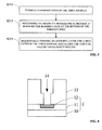
- FIG. 1 a flow chart of an exemplary process for fabricating a contact via is shown in accordance with some embodiments of the present invention.
- a semiconductor substrate 10 can be provided.
- a material of the semiconductor substrate 10 may be silicon or polycrystalline silicon. In some other embodiments, a material of the semiconductor substrate 10 can be selected from silicon, germanium, gallium arsenide and silicon germanium compound, or any other suitable semiconductor material.
- the semiconductor substrate 10 may have an epitaxial layer, or have a silicon on an epitaxial layer. In some embodiments, the semiconductor substrate 10 may include one or more device structures that are formed on the semiconductor substrate 10.
- a first dielectric layer 11 can be formed on the semiconductor substrate 10.
- the first dielectric layer 11 can include a buffer layer 12 that is formed inside of the first dielectric layer 11.
- a combination of the semiconductor substrate 10, the first dielectric layer 11, and the buffer layer 12 can constitute base structure 1.
- a material of the buffer layer 12 may be metallic copper. In some other embodiments, a material of the buffer layer 12 may be any other suitable conductive materials, such as aluminum, etc.
- a second dielectric layer 13 can be formed on the base structure 1.
- the second dielectric layer 13 can cover the first dielectric layer 11 and the buffer layer 12.
- a material of the second dielectric layer 13 may be silicon oxide, silicon nitride, or silicon carbon nitride.
- the second dielectric layer 13 can be made of a low-K dielectric material having a dielectric constant between 2.0 to 3.0, such as Black Diamond (BDII: SiOCH).
- a thickness of the Black Diamond (BDII: SiOCH) can be in a range from 1500 ⁇ to 3000 ⁇ .
- the second dielectric layer 13 can be formed by using a physical vapor deposition (PVD) process. In some other embodiments, the second dielectric layer 13 may be formed by using any other suitable process, such as a chemical vapor deposition (CVD) process.
- PVD physical vapor deposition
- CVD chemical vapor deposition
- a through hole 14 can be formed in the second dielectric layer 13.
- the through hole 14 can be formed by using a damascene process.
- the through hole 14 can penetrate through the second dielectric layer 13 to expose the surface of the buffer layer 12.
- An opening width of the through hole 14 can be in a range from 30nm to 100nm.
- a depth of the through hole 14 can be in a range from 100nm to 300nm.
- a cleaning process can be performed to the surface the buffer layer 12 to remove by-products that are generated on the surface of the buffer layer 12 during the process for forming the through hole.
- the bottom of the through hole 14 can be washed firstly.
- the etching agent can interact with the surface of the buffer layer 12 to generate by-products including CuF 2 , CuN, CuCN, etc.
- a cleaning agent can be selected from HF solution, H 2 SO 4 solution, HCl solution, HNO 3 solution, NH 4 OH solution, and any suitable combination thereof.
- an HF solution can be used as the cleaning agent.
- a volume ratio of H 2 O and HF can be in a range from 50:1 to 5000:1.
- a roughening treatment can be performed on the surface of the buffer layer 12 to increase the surface roughness of the buffer layer 12.
- the roughening treatment may be performed by using a wet etching method.
- FIG. 2 a flow chart of an exemplary process for roughening a surface of a buffer layer is shown in accordance with some embodiments of the present invention.
- an oxidation treatment can be performed to oxidize the surface of the buffer layer 12 to form an oxide layer 20.
- hydrogen peroxide solution can be used to oxidize the surface of the copper buffer layer 12 to form a copper oxide layer 20.
- a volume ratio of H 2 O and H 2 O 2 can be in a range from 5:1 to 10:1.
- a processing time of the oxidation treatment can be in a range from 5s to 20s.
- the oxide layer 20 on the surface of the buffer layer 20 can be removed.
- a hydrofluoric acid solution can be used to remove the oxide layer 20.
- a volume ratio of H 2 O and HF can be in a range from 50:1 to 5000:1.
- a processing time for applying the hydrofluoric acid solution can be in a range from 5s to 20s.
- the hydrofluoric acid solution can have a volume ratio of H 2 O and HF as 1000: 1.
- the generated copper oxide layer may have an uneven thickness. Therefore, after removing the copper oxide layer, the remained copper metal of the buffer layer 12 may have a rough surface. As such, a bonding force between the copper surface of the buffer layer 12 and the barrier layer to be formed subsequently may be relatively weak. In that case, the subsequently barrier layer deposited on the bottom of the through hole 14 may be easily bombarding out from the buffer layer by, e.g., argon ions.
- the surface treatment to the buffer layer 12 can further include a roughening process.
- the roughening process can be an argon ion bombardment process, or a dry etching process.
- an argon gas flow rate can be in a range from 4sccm to 50sccm.
- An RF power applied to an RF coil can be in a range from 0.5KW to 5KW.
- An AC bias power applied to a wafer can be in a range from 200W to 1000W.
- a bombardment duration time can be from 2s to 15s.
- CClF 3 or CF 4 can be used as an etching agent.
- a duration time of the dry etching process can be from 1s to 5s.
- FIG. 3 illustrates a flow chart of an exemplary process for filling a through hole in accordance with some embodiments of the present invention.
- a barrier layer 15 can be formed on the side walls and the bottom of the through hole 14.
- the barrier layer 15 can be used to prevent the diffusion of the metal atoms of the conductive material that is to be filled into the through hole subsequently. Without the barrier layer 15, the metal atoms of the conductive material can diffuse into the base structure 10, the first dielectric layer 11, and the second dielectric layer 13.
- the barrier layer 15 can include a first barrier layer 151 and a second barrier layer 152 located on the first barrier layer 151.
- the first barrier layer 151 includes one portion 151a on the side walls of the through hole 14, and another portion 151b on the bottom of the through hole 14.
- the second barrier layer 152 includes one portion 152a on the side walls of the through hole 14, and another portion 152b on the bottom of the through hole 14.
- a material of the first barrier 151 can be tantalum nitride
- a material of the second barrier layer 152 can be tantalum.
- a process for forming the barrier layer 15 can include forming the first barrier layer 151 on the side walls and the bottom of the through hole 14, and then form the second barrier layers 152 on the first barrier layer 151.
- PVD physical vapor deposition
- a nitrogen flow rate can be from 18sccm to 30sccm
- an argon gas flow rate can be from 4sccm to 20sccm
- a DC power of the physical bombardment can be from 10KW to 30KW
- an AC bias power applied to the wafer can be from 100W to 1000W.
- an argon gas flow rate can be from 4sccm to 20sccm
- a DC power of the physical bombardment cam be from 10KW to 30KW
- an AC bias power applied to the wafer can be from 100W to 1000W.
- each of the formed first barrier layer 151 and the second barrier layer 152 can be in the range from 20 ⁇ to 50 ⁇ .
- the thicknesses of the portion 151b of the first barrier layer 151 (e.g., tantalum nitride layer) and the portion 152b of the second barrier layer 152 (e.g., tantalum layer) at the bottom of the through hole 14 are the key factors to impact the resistance of the contact via to be form.
- a bias deposition process can be performed in some embodiments. That is, during the deposition processes to form the first barrier layer 151 and the second barrier layer 152, a bias with a certain power can be applied to the wafer.
- a bias power can be from 100W to 1000W
- an argon gas flow rate can be from 4sccm to 20sccm
- a DC voltage power applied to the target can be from 10KW to 30KW.
- the barrier layer 15 when the barrier layer 15 is deposited, a portion of the barrier layer 15 that has been deposited at the bottom of the though hole 14 can be bombarded by the subsequent tantalum nitride/tantalum atoms up towards the side walls of the through hole 14.
- the surface of the buffer layer 12 has been roughened, a binding force between the buffer layer 12 and the barrier layer 15 can be relatively weak. Therefore, the portion of the barrier layer 15 deposited at the bottom of the though hole 14 can be bombarded out more easily. Thus, the thickness of the portion 151b of the first barrier layer 151 and the portion 152b of the second barrier layer 152 at the bottom of the through hole 14 can be further reduced. In the meantime, a coverage rate of the portion 151a of the first barrier layer 151 and the portion 152a of the second barrier layer 152 on the side walls of the through hole 14 can be improved.
- argon ions can be used to bombard the barrier layer 15 at the bottom of the through hole 14.
- an argon gas flow rate can be from 5sccm to 50sccm.
- a radio frequency (RF) coil can be installed in the process chamber, and an RF power applied to the RF coil can be from 10kW to 30kW to ionize the argon gas.
- An AC power applied on the wafer can be from 500W to 1000W to accelerate the argon ions.
- a duration time of the bombardment process can be from 2s to 15s.
- the improved bombardment efficiency can avoid using a high power in the argon ion bombardment. Therefore, it can be ensured that the damages to the first dielectric layer 11 and second dielectric layer 13 can be eliminated during the argon ion bombardment process.
- an adhesive layer and a seed layer can be sequentially formed in the through hole 14, and the through hole 14 can be filled by using an electro chemical plating (ECP) process.
- ECP electro chemical plating
- an adhesive layer 30 can be formed in the through hole 14.
- the adhesive layer 30 can be used to ensure a continuous growth of the seed layer to be formed subsequently.
- a material of the adhesive material layer 30 may be tantalum, titanium, or any other suitable material.
- the adhesive layer 30 can be formed by using a physical vapor deposition (PVD) process. During the deposition process, a DC power of the physical bombardment can be from 10KW to 30KW, and AC bias power applied to the wafer can be from 100W to 1000W.
- the adhesive layer 30 may be formed by using a chemical vapor deposition (CVD) process, an atomic layer deposition (ALD) process, etc. A thickness of the adhesive layer 30 can be from 10 ⁇ to 30 ⁇ .
- a seed layer 40 can be formed in the through hole 14.
- a material of the seed layer 40 is related to the filling material used in the subsequent filling process.
- metal copper is used for the wire material, and the seed layer 40 is also made of copper.
- the copper seed layer can be formed by using a physical vapor deposition (PVD) process.
- a DC power applied to the target can be from 10KW to 50KW.
- a thickness of the copper seed layer can be from 200 ⁇ to 800 ⁇ .
- a filling process can be performed to fill conductive material 50 into the through hole 14.
- the conductive material 50 can be selected from tungsten, aluminum, silver, chromium, molybdenum, nickel, palladium, platinum, titanium, tantalum, copper, or any suitable combination thereof.
- the conductive material 50 is copper.
- the filling process to fill conductive material 50 into the through hole 14 can be realized by using an electro chemical plating (ECP) process.
- ECP electro chemical plating
- a planarization process can be performed to planarize the top surface of the filled through hole 14.
- CMP chemical mechanical polishing
- a contact via structure and a fabricating method thereof are provided.
- a roughening treatment can be performed to the surface of the buffer layer before forming the barrier layer, such that the binding force between the barrier layer and the buffer layer at the bottom of the through hole becomes weaker, which may facilitate to use an argon ion bombardment process to reduce the thickness of the barrier layer on the surface of the buffer layer. Therefore, the improved bombardment efficiency can avoid using a high power in the argon ion bombardment to eliminate the damages to the dielectric layer during the argon ion bombardment process. That is, under the premise of reliability, the resistance of the contact via can be effectively reduced.
- a buffer layer is inside of a substrate, a dielectric layer can cover the substrate and the buffer layer, and a through hole is in the dielectric layer.
- a surface of the buffer layer at the bottom of the through hole is a roughened surface.
- a barrier layer is in the through hole, a thickness of one portion of the barrier layer at the bottom of the through hole is less than a thickness of another portion of the barrier layer on the sidewalls of the through hole.
- An adhesive layer is on the barrier layer in the through hole, and a seed layer on the adhesive layer in the through hole. A conductive material filled in the through hole. Since the disclosed contact via structure has a thickness reduced barrier layer on the bottom of the through hole, the resistance of the contact via can be effectively reduced.
Landscapes
- Internal Circuitry In Semiconductor Integrated Circuit Devices (AREA)
- Physics & Mathematics (AREA)
- Engineering & Computer Science (AREA)
- Plasma & Fusion (AREA)
Abstract
Description
- This application claims the priority of Chinese patent application No.
201510703687.X, filed on October 26,2015 - The present invention generally relates to the field of semiconductor technologies and, more particularly, relates to a contact via structure and a method for fabricating the contact via structure.
- In existing integrated circuits, an interconnection between an upper layer and a lower layer can be generally achieved by using one or more contact vias. A specific process for forming a contact via can include the following steps. Firstly, a dielectric layer can be deposited. Then, a through hole can be formed in the dielectric layer by using photolithography technique and an etching process. Next, a barrier layer and a seed layer can be sequentially formed by using a physical vapor deposition (PVD) process. Then the through hole can be filled by using an electro chemical plating (ECP) method. Finally, a top surface of the filled through hole can be planarized by using a chemical mechanical polishing (CMP) method.
- However, during the deposition process for forming the barrier layer, a portion of the barrier layer can be deposited on the bottom of the through hole, which can increase the resistance of the contact via. Accordingly, it is desired to provide a method to reduce the resistance of the contact via.
- In accordance with some embodiments of the present invention, a contact via structure and a fabricating method thereof is provided.
- A first aspect of the present invention provides a method for forming a contact via structure, comprising: providing a substrate; forming a buffer layer in the substrate; forming a dielectric layer covering the substrate and the buffer layer; forming a through hole in the dielectric layer, wherein a bottom of the through hole exposes a surface of the buffer layer; performing a roughening treatment to the exposed surface of the buffer layer to increase a roughness of the exposed surface of the buffer layer; and filling a conductive material into the through hole to form a contact via.
- The roughening treatment may comprise: performing an oxidization process to the exposed surface of the buffer layer to form an oxidized layer; and removing the oxidized layer.
- The oxidization process may comprise: using a hydrogen peroxide solution to oxidize the exposed surface of the buffer layer, wherein: a volume ratio of H2O and H2O2 in the hydrogen peroxide solution is in a range from 5:1 to 10:1; and a duration time of the oxidation process is in a range from 5s to 20s.
- Removing the oxidized layer may comprise: using a hydrofluoric acid solution to remove the oxide layer, wherein: a volume ratio of H2O and HF in the hydrofluoric acid solution is in a range from 50:1 to 5000:1; and a processing time of to apply the hydrofluoric acid solution is in a range from 5s to 20s.
- The roughening treatment may comprise: performing an argon ion bombardment process to roughen the exposed surface of the buffer layer.
- The argon ion bombardment process may comprise: an argon gas flow rate in a range from 4sccm to 50sccm; a radio frequency (RF) power applied to an RF coil in a range from 0.5KW to 5KW; an alternating current (AC) bias power applied to a wafer in a range from 200W to 1000W; and a duration time of the argon ion bombardment process in a range from 2s to 15s.
- The roughening treatment may comprise: performing a dry etching process to roughen the exposed surface of the buffer layer.
- The dry etching process may comprise: using CClF3 or CF4 as an etching agent having a duration time of the dry etching process in a range from 1s to 5s.
- Before performing the roughening treatment, a cleaning process may be performed to remove by-products on the exposed surface of the buffer layer.
- A cleaning agent of the cleaning process may be selected from HF solution, H2SO4 solution, HCl solution, HNO3 solution, NH4OH solution, and a combination thereof.
- A cleaning agent of the cleaning process may be HF solution. A volume ratio of H2O and HF in the HF solution may be in a range from 50:1 to 5000:1.
- After performing the roughening treatment, a barrier layer may be formed in the through hole.
- Forming the barrier layer may comprise: using two physical vapor deposition (PVD) processes to form a tantalum nitride layer and a tantalum layer; wherein in each PVD process, a nitrogen flow rate is from 18sccm to 30sccm, an argon gas flow rate is from 4sccm to 20sccm, a DC power of physical bombardment is from 10KW to 30KW, and an AC bias power applied to a wafer is from 100W to 1000W.
- Forming the barrier layer may comprise: reducing a thickness of a portion of the barrier layer at the bottom of the through hole.
- Reducing the thickness of the portion of the barrier layer at the bottom of the through hole may comprise: performing an argon ion bombardment process to bombard the barrier layer at the bottom of the through hole; wherein an argon gas flow rate is in a range from 5sccm to 50sccm; an RF power applied on a RF coil is in a range from 10kW to 30kW to ionize the argon gas; an AC power applied on a wafer is in a range from 500W to 1000W to accelerate the argon ions; and a duration time of the argon ion bombardment process is in a range from 2s to 15s.
- Before filling the through hole, an adhesive layer and a seed layer may be sequentially formed on the barrier layer in the through hole. After filling the through hole, a planarization process may be performed to planarize the top surface of the contact via.
- A second aspect of the present invention provides a contact via structure, comprising: a substrate; a buffer layer inside of the substrate; a dielectric layer covering the substrate and the buffer layer; a through hole in the dielectric layer, wherein a surface of the buffer layer at the bottom of the through hole is a roughened surface; a barrier layer in the through hole, wherein a thickness of one portion of the barrier layer at the bottom of the through hole is less than a thickness of another portion of the barrier layer on the sidewalls of the through hole; an adhesive layer on the barrier layer in the through hole; a seed layer on the adhesive layer in the through hole; and a conductive material filled in the through hole.
- The barrier layer may comprise: a tantalum nitride layer and a tantalum layer. A thickness of the tantalum nitride layer may be in a range 20Å to 50Å. A thickness of the tantalum layer may be in a range 20Å to 50Å.
- A material of the dielectric layer may be Black Diamond (BDII: SiOCH). A thickness of the dielectric layer may be in a range from 1500Å to 3000Å. A bonding force between the barrier layer and the buffer layer at the bottom of the through hole may be configured to be less than a bonding force between the barrier layer and the dielectric layer at the side wall of the through hole.
- The through hole may have a single damascene structure. An opening width of the through hole may be in a range from 30nm to 100nm. A depth of the through hole may be in a range from 100nm to 300nm.
- Other aspects of the present invention can be understood by those skilled in the art in light of the description, the claims, and the drawings of the present invention.
- Various objects, features, and advantages of the present invention can be more fully appreciated with reference to the following detailed description of the present invention when considered in connection with the following drawings, in which like reference numerals identify like elements. It should be noted that the following drawings are merely examples for illustrative purposes according to various disclosed embodiments and are not intended to limit the scope of the present invention which defined by the claims.
-
FIG. 1 illustrates a flow chart of an exemplary process for fabricating a contact via in accordance with some embodiments of the present invention; -
FIG. 2 illustrates a flow chart of an exemplary process for roughening a surface of a buffer layer in accordance with some embodiments of the present invention; -
FIG. 3 illustrates a flow chart of an exemplary process for filling a through hole in accordance with some embodiments of the present invention; and -
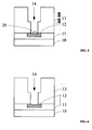
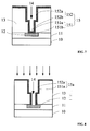
FIGS. 4-12 illustrate cross sectional structures of an exemplary contact via corresponding to certain stages of an exemplary fabricating process consistent with some embodiments of the present invention. - The present invention provides a contact via structure and a fabricating method thereof. In the following, details of the contact via and the fabricating method are described in connection with the drawings.
- Note that, a contact via having a single damascene structure is described herein as an example. However, the disclosed fabricating method can be applied to any other contact vias having different suitable structures, such as a plug structure, a straight through-hole structure, etc.
- Turning to
FIG. 1 , a flow chart of an exemplary process for fabricating a contact via is shown in accordance with some embodiments of the present invention. - Referring to
step 11 inFIG. 1 and as illustrated inFIG. 4 , asemiconductor substrate 10 can be provided. - In some embodiments, a material of the
semiconductor substrate 10 may be silicon or polycrystalline silicon. In some other embodiments, a material of thesemiconductor substrate 10 can be selected from silicon, germanium, gallium arsenide and silicon germanium compound, or any other suitable semiconductor material. Thesemiconductor substrate 10 may have an epitaxial layer, or have a silicon on an epitaxial layer. In some embodiments, thesemiconductor substrate 10 may include one or more device structures that are formed on thesemiconductor substrate 10. - Referring to
step S 13 inFIG. 1 and as illustrated inFIG. 4 , a firstdielectric layer 11 can be formed on thesemiconductor substrate 10. The firstdielectric layer 11 can include abuffer layer 12 that is formed inside of the firstdielectric layer 11. - A combination of the
semiconductor substrate 10, thefirst dielectric layer 11, and thebuffer layer 12 can constitutebase structure 1. - In some embodiments, a material of the
buffer layer 12 may be metallic copper. In some other embodiments, a material of thebuffer layer 12 may be any other suitable conductive materials, such as aluminum, etc. - Referring to step S14 in
FIG. 1 and as illustrated inFIG. 4 , asecond dielectric layer 13 can be formed on thebase structure 1. Thesecond dielectric layer 13 can cover thefirst dielectric layer 11 and thebuffer layer 12. - A material of the
second dielectric layer 13 may be silicon oxide, silicon nitride, or silicon carbon nitride. In some other embodiments, thesecond dielectric layer 13 can be made of a low-K dielectric material having a dielectric constant between 2.0 to 3.0, such as Black Diamond (BDII: SiOCH). A thickness of the Black Diamond (BDII: SiOCH) can be in a range from 1500Å to 3000Å. - The
second dielectric layer 13 can be formed by using a physical vapor deposition (PVD) process. In some other embodiments, thesecond dielectric layer 13 may be formed by using any other suitable process, such as a chemical vapor deposition (CVD) process. - Referring to step S15 in
FIG. 1 and as illustrated inFIG. 4 , a throughhole 14 can be formed in thesecond dielectric layer 13. The throughhole 14 can be formed by using a damascene process. The throughhole 14 can penetrate through thesecond dielectric layer 13 to expose the surface of thebuffer layer 12. An opening width of the throughhole 14 can be in a range from 30nm to 100nm. A depth of the throughhole 14 can be in a range from 100nm to 300nm. - In some embodiments, before performing a roughening treatment towards the
buffer layer 12, a cleaning process can be performed to the surface thebuffer layer 12 to remove by-products that are generated on the surface of thebuffer layer 12 during the process for forming the through hole. - Referring to step S17 in
FIG. 1 , the bottom of the throughhole 14 can be washed firstly. Specifically, when thebuffer layer 12 contains metal copper, during the etching process for forming the throughhole 14, the etching agent can interact with the surface of thebuffer layer 12 to generate by-products including CuF2, CuN, CuCN, etc. In order to remove the by-products, a cleaning agent can be selected from HF solution, H2SO4 solution, HCl solution, HNO3 solution, NH4OH solution, and any suitable combination thereof. In one embodiment, an HF solution can be used as the cleaning agent. In the HF solution, a volume ratio of H2O and HF can be in a range from 50:1 to 5000:1. - Referring to step S19 in
FIG. 1 , in order to reduce a binding force between thebuffer layer 12 and a barrier layer to be formed subsequently, a roughening treatment can be performed on the surface of thebuffer layer 12 to increase the surface roughness of thebuffer layer 12. The roughening treatment may be performed by using a wet etching method. - Turning to
FIG. 2 , a flow chart of an exemplary process for roughening a surface of a buffer layer is shown in accordance with some embodiments of the present invention. - Referring to step S 191 in
FIG. 2 and as illustrated inFIG. 5 , an oxidation treatment can be performed to oxidize the surface of thebuffer layer 12 to form anoxide layer 20. In some embodiments, hydrogen peroxide solution can be used to oxidize the surface of thecopper buffer layer 12 to form acopper oxide layer 20. In the hydrogen peroxide solution, a volume ratio of H2O and H2O2 can be in a range from 5:1 to 10:1. A processing time of the oxidation treatment can be in a range from 5s to 20s. - Referring to step S193 in
FIG. 2 and as illustrated inFIG. 5 , theoxide layer 20 on the surface of thebuffer layer 20 can be removed. In some embodiments, a hydrofluoric acid solution can be used to remove theoxide layer 20. In the hydrofluoric acid solution, a volume ratio of H2O and HF can be in a range from 50:1 to 5000:1. A processing time for applying the hydrofluoric acid solution can be in a range from 5s to 20s. In one embodiment, the hydrofluoric acid solution can have a volume ratio of H2O and HF as 1000: 1. - Note that, during a short processing time of the oxidation treatment, the generated copper oxide layer may have an uneven thickness. Therefore, after removing the copper oxide layer, the remained copper metal of the
buffer layer 12 may have a rough surface. As such, a bonding force between the copper surface of thebuffer layer 12 and the barrier layer to be formed subsequently may be relatively weak. In that case, the subsequently barrier layer deposited on the bottom of the throughhole 14 may be easily bombarding out from the buffer layer by, e.g., argon ions. - It also should be noted that, the surface treatment to the
buffer layer 12 can further include a roughening process. The roughening process can be an argon ion bombardment process, or a dry etching process. - In the argon ion bombardment process, an argon gas flow rate can be in a range from 4sccm to 50sccm. An RF power applied to an RF coil can be in a range from 0.5KW to 5KW. An AC bias power applied to a wafer can be in a range from 200W to 1000W. A bombardment duration time can be from 2s to 15s.
- In the dry etching process, CClF3 or CF4 can be used as an etching agent. A duration time of the dry etching process can be from 1s to 5s.
- Turning back to
FIG. 1 , in step S21, the throughhole 14 can be filled.FIG. 3 illustrates a flow chart of an exemplary process for filling a through hole in accordance with some embodiments of the present invention. - Referring to step S211 in
FIG. 3 and as illustrated inFIG. 7 , abarrier layer 15 can be formed on the side walls and the bottom of the throughhole 14. Thebarrier layer 15 can be used to prevent the diffusion of the metal atoms of the conductive material that is to be filled into the through hole subsequently. Without thebarrier layer 15, the metal atoms of the conductive material can diffuse into thebase structure 10, thefirst dielectric layer 11, and thesecond dielectric layer 13. - Specifically, the
barrier layer 15 can include afirst barrier layer 151 and asecond barrier layer 152 located on thefirst barrier layer 151. Thefirst barrier layer 151 includes oneportion 151a on the side walls of the throughhole 14, and anotherportion 151b on the bottom of the throughhole 14. Thesecond barrier layer 152 includes oneportion 152a on the side walls of the throughhole 14, and anotherportion 152b on the bottom of the throughhole 14. In some embodiments, a material of thefirst barrier 151 can be tantalum nitride, and a material of thesecond barrier layer 152 can be tantalum. - A process for forming the
barrier layer 15 can include forming thefirst barrier layer 151 on the side walls and the bottom of the throughhole 14, and then form the second barrier layers 152 on thefirst barrier layer 151. - In some embodiments, a physical vapor deposition (PVD) process can be used for forming the
first barrier layer 151 and thesecond barrier layer 152. - During the deposition process for forming the
first barrier layer 151, a nitrogen flow rate can be from 18sccm to 30sccm, an argon gas flow rate can be from 4sccm to 20sccm, a DC power of the physical bombardment can be from 10KW to 30KW, and an AC bias power applied to the wafer can be from 100W to 1000W. - During the deposition process for forming the
second barrier layer 152, an argon gas flow rate can be from 4sccm to 20sccm, a DC power of the physical bombardment cam be from 10KW to 30KW, and an AC bias power applied to the wafer can be from 100W to 1000W. - The thickness of each of the formed
first barrier layer 151 and thesecond barrier layer 152 can be in the range from 20Å to 50Å. - Note that, the thicknesses of the
portion 151b of the first barrier layer 151 (e.g., tantalum nitride layer) and theportion 152b of the second barrier layer 152 (e.g., tantalum layer) at the bottom of the throughhole 14 are the key factors to impact the resistance of the contact via to be form. - In order to improve the step coverage of the tantalum nitride and the tantalum and reduce the thickness of the
portion 151b of thefirst barrier layer 151 and theportion 152b of thesecond barrier layer 152 at the bottom of the throughhole 14, a bias deposition process can be performed in some embodiments. That is, during the deposition processes to form thefirst barrier layer 151 and thesecond barrier layer 152, a bias with a certain power can be applied to the wafer. - Specifically, a bias power can be from 100W to 1000W, an argon gas flow rate can be from 4sccm to 20sccm, and a DC voltage power applied to the target can be from 10KW to 30KW.
- As such, when the
barrier layer 15 is deposited, a portion of thebarrier layer 15 that has been deposited at the bottom of the thoughhole 14 can be bombarded by the subsequent tantalum nitride/tantalum atoms up towards the side walls of the throughhole 14. - Since the surface of the
buffer layer 12 has been roughened, a binding force between thebuffer layer 12 and thebarrier layer 15 can be relatively weak. Therefore, the portion of thebarrier layer 15 deposited at the bottom of the thoughhole 14 can be bombarded out more easily. Thus, the thickness of theportion 151b of thefirst barrier layer 151 and theportion 152b of thesecond barrier layer 152 at the bottom of the throughhole 14 can be further reduced. In the meantime, a coverage rate of theportion 151a of thefirst barrier layer 151 and theportion 152a of thesecond barrier layer 152 on the side walls of the throughhole 14 can be improved. - Referring to step S213 in
FIG. 3 and as illustrated inFIG. 8 , to reduce the thickness of theportion 151b of thefirst barrier layer 151 and theportion 152b of thesecond barrier layer 152 at the bottom of the throughhole 14, argon ions can be used to bombard thebarrier layer 15 at the bottom of the throughhole 14. - In some embodiments, during the argon ion bombardment process, an argon gas flow rate can be from 5sccm to 50sccm. A radio frequency (RF) coil can be installed in the process chamber, and an RF power applied to the RF coil can be from 10kW to 30kW to ionize the argon gas. An AC power applied on the wafer can be from 500W to 1000W to accelerate the argon ions. A duration time of the bombardment process can be from 2s to 15s.
- As described above, since a bonding force between the
barrier layer 15 and thebuffer layer 12 is relatively small, a relatively low power used in the argon ion bombardment process is able to remove a relatively large amount of thebarrier layer 15 at the bottom of the through holes 14. That is, the improved bombardment efficiency can avoid using a high power in the argon ion bombardment. Therefore, it can be ensured that the damages to thefirst dielectric layer 11 and seconddielectric layer 13 can be eliminated during the argon ion bombardment process. - Referring to step S215 in
FIG. 3 , an adhesive layer and a seed layer can be sequentially formed in the throughhole 14, and the throughhole 14 can be filled by using an electro chemical plating (ECP) process. - Turning to
FIG. 9 , anadhesive layer 30 can be formed in the throughhole 14. Theadhesive layer 30 can be used to ensure a continuous growth of the seed layer to be formed subsequently. In some embodiments, a material of theadhesive material layer 30 may be tantalum, titanium, or any other suitable material. Theadhesive layer 30 can be formed by using a physical vapor deposition (PVD) process. During the deposition process, a DC power of the physical bombardment can be from 10KW to 30KW, and AC bias power applied to the wafer can be from 100W to 1000W. In some other embodiments, theadhesive layer 30 may be formed by using a chemical vapor deposition (CVD) process, an atomic layer deposition (ALD) process, etc. A thickness of theadhesive layer 30 can be from 10Å to 30Å. - Turning to
FIG. 10 , aseed layer 40 can be formed in the throughhole 14. A material of theseed layer 40 is related to the filling material used in the subsequent filling process. In one embodiment, metal copper is used for the wire material, and theseed layer 40 is also made of copper. The copper seed layer can be formed by using a physical vapor deposition (PVD) process. A DC power applied to the target can be from 10KW to 50KW. A thickness of the copper seed layer can be from 200Å to 800Å. - Turning to
FIG. 11 , a filling process can be performed to fillconductive material 50 into the throughhole 14. Theconductive material 50 can be selected from tungsten, aluminum, silver, chromium, molybdenum, nickel, palladium, platinum, titanium, tantalum, copper, or any suitable combination thereof. In one embodiment, theconductive material 50 is copper. Specifically, the filling process to fillconductive material 50 into the throughhole 14 can be realized by using an electro chemical plating (ECP) process. - Referring back to step S23 of
FIG. 1 and as illustrated in 12, after the filling process, a planarization process can be performed to planarize the top surface of the filled throughhole 14. Specifically, a chemical mechanical polishing (CMP) process can be used to planarize the top surface of the filled throughhole 14 to form a contact via 60. - The provision of the examples described herein (as well as clauses phrased as "such as," "e.g.," "including," and the like) should not be interpreted as limiting the claimed subject matter to the specific examples; rather, the examples are intended to illustrate only some of many possible aspects.
- Accordingly, a contact via structure and a fabricating method thereof are provided. In the disclosed fabricating method, a roughening treatment can be performed to the surface of the buffer layer before forming the barrier layer, such that the binding force between the barrier layer and the buffer layer at the bottom of the through hole becomes weaker, which may facilitate to use an argon ion bombardment process to reduce the thickness of the barrier layer on the surface of the buffer layer. Therefore, the improved bombardment efficiency can avoid using a high power in the argon ion bombardment to eliminate the damages to the dielectric layer during the argon ion bombardment process. That is, under the premise of reliability, the resistance of the contact via can be effectively reduced.
- In the disclosed contact via structure, a buffer layer is inside of a substrate, a dielectric layer can cover the substrate and the buffer layer, and a through hole is in the dielectric layer. A surface of the buffer layer at the bottom of the through hole is a roughened surface. A barrier layer is in the through hole, a thickness of one portion of the barrier layer at the bottom of the through hole is less than a thickness of another portion of the barrier layer on the sidewalls of the through hole. An adhesive layer is on the barrier layer in the through hole, and a seed layer on the adhesive layer in the through hole. A conductive material filled in the through hole. Since the disclosed contact via structure has a thickness reduced barrier layer on the bottom of the through hole, the resistance of the contact via can be effectively reduced.
Claims (15)
- A method for fabricating a contact via structure, comprising:providing a substrate;forming a buffer layer in the substrate;forming a dielectric layer covering the substrate and the buffer layer;forming a through hole in the dielectric layer, wherein a bottom of the through hole exposes a surface of the buffer layer;performing a roughening treatment to the exposed surface of the buffer layer to increase a roughness of the exposed surface of the buffer layer; andfilling a conductive material into the through hole to form a contact via.
- The method of claim 1, wherein the roughening treatment comprises:performing an oxidization process to the exposed surface of the buffer layer to form an oxidized layer; andremoving the oxidized layer.
- The method of claim 2, wherein the oxidization process comprises:using a hydrogen peroxide solution to oxidize the exposed surface of the buffer layer, wherein: a volume ratio of H2O and H2O2 in the hydrogen peroxide solution is in a range from 5:1 to 10:1; and a duration time of the oxidation process is in a range from 5s to 20s;or alternatively,using a hydrofluoric acid solution to remove the oxide layer, wherein: a volume ratio of H2O and HF in the hydrofluoric acid solution is in a range from 50:1 to 5000:1; and a processing time of to apply the hydrofluoric acid solution is in a range from 5s to 20s.
- The method of any one of the claims 1-3, wherein the roughening treatment comprises:performing an argon ion bombardment process to roughen the exposed surface of the buffer layer,wherein preferably the argon ion bombardment process comprises: an argon gas flow rate in a range from 4sccm to 50sccm; a radio frequency (RF) power applied to an RF coil in a range from 0.5KW to 5KW; an alternating current (AC) bias power applied to a wafer in a range from 200W to 1000W; and a duration time of the argon ion bombardment process in a range from 2s to 15s.
- The method of any one of the claims 1-4, wherein the roughening treatment comprises:performing a dry etching process to roughen the exposed surface of the buffer layer,wherein preferably the dry etching process comprises: using CClF3 or CF4 as an etching agent having a duration time of the dry etching process in a range from 1s to 5s.
- The method of any one of the claims 1-5, further comprising:before performing the roughening treatment, performing a cleaning process to remove by-products on the exposed surface of the buffer layer.
- The method of claim 6, wherein:a cleaning agent of the cleaning process is selected from HF solution, H2SO4 solution, HCl solution, HNO3 solution, NH4OH solution, and a combination thereof,wherein preferably a cleaning agent of the cleaning process is HF solution, and a volume ratio of H2O and HF in the HF solution is in a range from 50:1 to 5000:1.
- The method of any one of the claims 1-7, further comprising:after performing the roughening treatment, forming a barrier layer in the through hole.
- The method of claim 8, wherein forming the barrier layer comprises:using two physical vapor deposition (PVD) processes to form a tantalum nitride layer and a tantalum layer;wherein in each PVD process, a nitrogen flow rate is from 18sccm to 30sccm, an argon gas flow rate is from 4sccm to 20sccm, a DC power of physical bombardment is from 10KW to 30KW, and an AC bias power applied to a wafer is from 100W to 1000W.
- The method of claim 8 or 9, wherein forming the barrier layer comprises:reducing a thickness of a portion of the barrier layer at the bottom of the through hole,wherein preferably reducing the thickness of the portion of the barrier layer at the bottom of the through hole comprises: performing an argon ion bombardment process to bombard the barrier layer at the bottom of the through hole; wherein an argon gas flow rate is in a range from 5sccm to 50sccm; an RF power applied on a RF coil is in a range from 10kW to 30kW to ionize the argon gas; an AC power applied on a wafer is in a range from 500W to 1000W to accelerate the argon ions; and a duration time of the argon ion bombardment process is in a range from 2s to 15s.
- The method of any one of the claims 1-10, further comprising:before filling the through hole, sequentially forming an adhesive layer and a seed layer on the barrier layer in the through hole; andafter filling the through hole, performing a planarization process to planarize the top surface of the contact via.
- A contact via structure, comprising:a substrate;a buffer layer inside of the substrate;a dielectric layer covering the substrate and the buffer layer;a through hole in the dielectric layer, wherein a surface of the buffer layer at the bottom of the through hole is a roughened surface;a barrier layer in the through hole, wherein a thickness of one portion of the barrier layer at the bottom of the through hole is less than a thickness of another portion of the barrier layer on the sidewalls of the through hole;an adhesive layer on the barrier layer in the through hole;a seed layer on the adhesive layer in the through hole; anda conductive material filled in the through hole.
- The contact via structure of claim 12, wherein the barrier layer comprises:a tantalum nitride layer and a tantalum layer, whereina thickness of the tantalum nitride layer is in a range 20Å to 50Å; anda thickness of the tantalum layer is in a range 20Å to 50Å.
- The contact via structure of claim 12 or 13, wherein:a material of the dielectric layer is Black Diamond (BDII: SiOCH);a thickness of the dielectric layer is in a range from 1500Å to 3000Å; anda bonding force between the barrier layer and the buffer layer at the bottom of the through hole is less than a bonding force between the barrier layer and the dielectric layer at the side wall of the through hole.
- The contact via structure of any one of the claims 12-14, wherein:the through hole has a single damascene structure;an opening width of the through hole is in a range from 30nm to 100nm; anda depth of the through hole is in a range from 100nm to 300nm.
Applications Claiming Priority (1)
| Application Number | Priority Date | Filing Date | Title |
|---|---|---|---|
| CN201510703687.XA CN106611742B (en) | 2015-10-26 | 2015-10-26 | Method for forming contact hole |
Publications (2)
| Publication Number | Publication Date |
|---|---|
| EP3163605A2 true EP3163605A2 (en) | 2017-05-03 |
| EP3163605A3 EP3163605A3 (en) | 2017-08-23 |
Family
ID=57189826
Family Applications (1)
| Application Number | Title | Priority Date | Filing Date |
|---|---|---|---|
| EP16194579.5A Withdrawn EP3163605A3 (en) | 2015-10-26 | 2016-10-19 | Contact via structure and fabricating method thereof |
Country Status (3)
| Country | Link |
|---|---|
| US (1) | US9978677B2 (en) |
| EP (1) | EP3163605A3 (en) |
| CN (1) | CN106611742B (en) |
Cited By (1)
| Publication number | Priority date | Publication date | Assignee | Title |
|---|---|---|---|---|
| US11183455B2 (en) | 2020-04-15 | 2021-11-23 | International Business Machines Corporation | Interconnects with enlarged contact area |
Families Citing this family (17)
| Publication number | Priority date | Publication date | Assignee | Title |
|---|---|---|---|---|
| CN107591357B (en) * | 2016-07-07 | 2020-09-04 | 中芯国际集成电路制造(北京)有限公司 | Interconnect structure and method of making the same |
| JP2018107227A (en) * | 2016-12-26 | 2018-07-05 | ソニーセミコンダクタソリューションズ株式会社 | SEMICONDUCTOR DEVICE, SEMICONDUCTOR DEVICE MANUFACTURING METHOD, AND SOLID-STATE IMAGING ELEMENT |
| US10283404B2 (en) * | 2017-03-30 | 2019-05-07 | Lam Research Corporation | Selective deposition of WCN barrier/adhesion layer for interconnect |
| US10461149B1 (en) * | 2018-06-28 | 2019-10-29 | Micron Technology, Inc. | Elevationally-elongated conductive structure of integrated circuitry, method of forming an array of capacitors, method of forming DRAM circuitry, and method of forming an elevationally-elongated conductive structure of integrated circuitry |
| US10475796B1 (en) | 2018-06-28 | 2019-11-12 | Micron Technology, Inc. | Method of forming an array of capacitors, a method of forming DRAM circuitry, and a method of forming an elevationally-elongated conductive structure of integrated circuitry |
| EP3723117A1 (en) | 2019-04-10 | 2020-10-14 | AT & S Austria Technologie & Systemtechnik Aktiengesellschaft | Component carrier and method of manufacturing the same |
| US11929280B2 (en) | 2020-09-22 | 2024-03-12 | Changxin Memory Technologies, Inc. | Contact window structure and method for forming contact window structure |
| CN114256134A (en) * | 2020-09-22 | 2022-03-29 | 长鑫存储技术有限公司 | Contact window structure and forming method thereof |
| EP4002437B1 (en) | 2020-09-22 | 2023-08-02 | Changxin Memory Technologies, Inc. | Method of forming a contact window structure |
| CN114256135A (en) | 2020-09-22 | 2022-03-29 | 长鑫存储技术有限公司 | Opening structure and forming method thereof, contact plug and forming method thereof |
| CN114256417A (en) | 2020-09-22 | 2022-03-29 | 长鑫存储技术有限公司 | Capacitor structure and forming method thereof |
| CN113173552B (en) * | 2021-04-09 | 2023-06-23 | 深圳清华大学研究院 | Large-scale super-slip components with conductive properties and their processing technology, large-scale super-slip systems |
| CN115020333A (en) * | 2022-05-24 | 2022-09-06 | 上海华力集成电路制造有限公司 | Method for improving edge defect of wafer |
| US12278152B2 (en) * | 2022-08-06 | 2025-04-15 | Nanya Technology Corporation | Semiconductor device with cushion structure and method for fabricating the same |
| EP4391741B1 (en) | 2022-12-22 | 2026-02-25 | AT & S Austria Technologie & Systemtechnik Aktiengesellschaft | Glass barrier layer product, and manufacture method |
| US20250038008A1 (en) * | 2023-07-28 | 2025-01-30 | Taiwan Semiconductor Manufacturing Company, Ltd. | Methods for chemical mechanical polishing and methods for forming an interconnect structure of a semiconductor device |
| WO2025114130A1 (en) | 2023-11-29 | 2025-06-05 | At & S Austria Technologie & Systemtechnik Aktiengesellschaft | A component carrier assembly and method for manufacturing a component carrier assembly |
Family Cites Families (10)
| Publication number | Priority date | Publication date | Assignee | Title |
|---|---|---|---|---|
| JPH09213801A (en) * | 1996-01-29 | 1997-08-15 | Sony Corp | Method of manufacturing semiconductor device having step of forming connection hole |
| TW480619B (en) * | 2001-04-17 | 2002-03-21 | United Microelectronics Corp | Cleaning method for dual damascene manufacture process |
| US6887786B2 (en) * | 2002-05-14 | 2005-05-03 | Applied Materials, Inc. | Method and apparatus for forming a barrier layer on a substrate |
| US6803309B2 (en) * | 2002-07-03 | 2004-10-12 | Taiwan Semiconductor Manufacturing Co., Ltd | Method for depositing an adhesion/barrier layer to improve adhesion and contact resistance |
| JP2005072384A (en) * | 2003-08-26 | 2005-03-17 | Matsushita Electric Ind Co Ltd | Manufacturing method of electronic device |
| US20060099786A1 (en) * | 2004-10-22 | 2006-05-11 | Taiwan Semiconductor Manufacturing Co. | Copper interconnect structure with modulated topography and method for forming the same |
| JP2006165189A (en) * | 2004-12-06 | 2006-06-22 | Nec Electronics Corp | Method of manufacturing semiconductor device |
| KR100707576B1 (en) * | 2005-06-03 | 2007-04-13 | 동부일렉트로닉스 주식회사 | Via hole formation method of semiconductor device |
| US7396762B2 (en) * | 2006-08-30 | 2008-07-08 | International Business Machines Corporation | Interconnect structures with linear repair layers and methods for forming such interconnection structures |
| JP2011119330A (en) * | 2009-12-01 | 2011-06-16 | Renesas Electronics Corp | Manufacturing method of semiconductor integrated circuit device |
-
2015
- 2015-10-26 CN CN201510703687.XA patent/CN106611742B/en active Active
-
2016
- 2016-10-19 EP EP16194579.5A patent/EP3163605A3/en not_active Withdrawn
- 2016-10-25 US US15/333,319 patent/US9978677B2/en active Active
Non-Patent Citations (1)
| Title |
|---|
| None |
Cited By (1)
| Publication number | Priority date | Publication date | Assignee | Title |
|---|---|---|---|---|
| US11183455B2 (en) | 2020-04-15 | 2021-11-23 | International Business Machines Corporation | Interconnects with enlarged contact area |
Also Published As
| Publication number | Publication date |
|---|---|
| US20170117218A1 (en) | 2017-04-27 |
| CN106611742A (en) | 2017-05-03 |
| EP3163605A3 (en) | 2017-08-23 |
| US9978677B2 (en) | 2018-05-22 |
| CN106611742B (en) | 2020-05-08 |
Similar Documents
| Publication | Publication Date | Title |
|---|---|---|
| US9978677B2 (en) | Contact via structure and fabricating method thereof | |
| US8415261B1 (en) | Capping before barrier-removal IC fabrication method | |
| US9768060B2 (en) | Systems and methods for electrochemical deposition on a workpiece including removing contamination from seed layer surface prior to ECD | |
| US7704886B2 (en) | Multi-step Cu seed layer formation for improving sidewall coverage | |
| CN106486416B (en) | Method of forming metal interconnect structure | |
| US8222142B2 (en) | Semiconductor device and method for manufacturing semiconductor device | |
| JP2002118109A (en) | Method for forming damascene wiring of semiconductor device and damascene wiring structure formed thereby | |
| US10937692B2 (en) | Method for reducing via RC delay | |
| US8765596B1 (en) | Atomic layer profiling of diffusion barrier and metal seed layers | |
| CN101240413A (en) | re-sputtered copper seed layer | |
| CN101510525B (en) | Method of forming integrated circuit structure | |
| US20140374907A1 (en) | Ultra-thin copper seed layer for electroplating into small features | |
| WO2008016004A1 (en) | Method for film formation, apparatus for film formation, computer program, and storage medium | |
| US8119525B2 (en) | Process for selective growth of films during ECP plating | |
| JP5667485B2 (en) | Semiconductor device manufacturing method and semiconductor device | |
| CN107895710B (en) | Copper filling process of via hole | |
| Killge et al. | Copper-based TSV: Interposer | |
| WO2009091830A2 (en) | Cu surface plasma treatment to improve gapfill window | |
| US20210391176A1 (en) | Overhang reduction using pulsed bias | |
| US7297630B2 (en) | Methods of fabricating via hole and trench | |
| CN106653680A (en) | Method for forming contact hole | |
| KR20060114215A (en) | Metal wiring formation method of semiconductor device | |
| TW410428B (en) | Process for improving sidewall coverage capability in filling metal to trench |
Legal Events
| Date | Code | Title | Description |
|---|---|---|---|
| PUAI | Public reference made under article 153(3) epc to a published international application that has entered the european phase |
Free format text: ORIGINAL CODE: 0009012 |
|
| STAA | Information on the status of an ep patent application or granted ep patent |
Free format text: STATUS: THE APPLICATION HAS BEEN PUBLISHED |
|
| AK | Designated contracting states |
Kind code of ref document: A2 Designated state(s): AL AT BE BG CH CY CZ DE DK EE ES FI FR GB GR HR HU IE IS IT LI LT LU LV MC MK MT NL NO PL PT RO RS SE SI SK SM TR |
|
| AX | Request for extension of the european patent |
Extension state: BA ME |
|
| RAP1 | Party data changed (applicant data changed or rights of an application transferred) |
Owner name: SEMICONDUCTOR MANUFACTURING INTERNATIONAL CORPORAT |
|
| PUAL | Search report despatched |
Free format text: ORIGINAL CODE: 0009013 |
|
| AK | Designated contracting states |
Kind code of ref document: A3 Designated state(s): AL AT BE BG CH CY CZ DE DK EE ES FI FR GB GR HR HU IE IS IT LI LT LU LV MC MK MT NL NO PL PT RO RS SE SI SK SM TR |
|
| AX | Request for extension of the european patent |
Extension state: BA ME |
|
| RIC1 | Information provided on ipc code assigned before grant |
Ipc: H01L 21/768 20060101AFI20170718BHEP |
|
| STAA | Information on the status of an ep patent application or granted ep patent |
Free format text: STATUS: REQUEST FOR EXAMINATION WAS MADE |
|
| 17P | Request for examination filed |
Effective date: 20180130 |
|
| RBV | Designated contracting states (corrected) |
Designated state(s): AL AT BE BG CH CY CZ DE DK EE ES FI FR GB GR HR HU IE IS IT LI LT LU LV MC MK MT NL NO PL PT RO RS SE SI SK SM TR |
|
| RAP1 | Party data changed (applicant data changed or rights of an application transferred) |
Owner name: SEMICONDUCTOR MANUFACTURING INTERNATIONAL (BEIJING Owner name: SEMICONDUCTOR MANUFACTURING INTERNATIONAL (SHANGHA |
|
| STAA | Information on the status of an ep patent application or granted ep patent |
Free format text: STATUS: EXAMINATION IS IN PROGRESS |
|
| 17Q | First examination report despatched |
Effective date: 20210203 |
|
| STAA | Information on the status of an ep patent application or granted ep patent |
Free format text: STATUS: THE APPLICATION IS DEEMED TO BE WITHDRAWN |
|
| 18D | Application deemed to be withdrawn |
Effective date: 20210615 |