EP3163511A1 - Multi-band rfid device - Google Patents
Multi-band rfid device Download PDFInfo
- Publication number
- EP3163511A1 EP3163511A1 EP15306709.5A EP15306709A EP3163511A1 EP 3163511 A1 EP3163511 A1 EP 3163511A1 EP 15306709 A EP15306709 A EP 15306709A EP 3163511 A1 EP3163511 A1 EP 3163511A1
- Authority
- EP
- European Patent Office
- Prior art keywords
- wave dipole
- frequency
- rfid
- operating
- module
- Prior art date
- Legal status (The legal status is an assumption and is not a legal conclusion. Google has not performed a legal analysis and makes no representation as to the accuracy of the status listed.)
- Granted
Links
Images



Classifications
-
- G—PHYSICS
- G06—COMPUTING OR CALCULATING; COUNTING
- G06K—GRAPHICAL DATA READING; PRESENTATION OF DATA; RECORD CARRIERS; HANDLING RECORD CARRIERS
- G06K19/00—Record carriers for use with machines and with at least a part designed to carry digital markings
- G06K19/06—Record carriers for use with machines and with at least a part designed to carry digital markings characterised by the kind of the digital marking, e.g. shape, nature, code
- G06K19/067—Record carriers with conductive marks, printed circuits or semiconductor circuit elements, e.g. credit or identity cards also with resonating or responding marks without active components
- G06K19/07—Record carriers with conductive marks, printed circuits or semiconductor circuit elements, e.g. credit or identity cards also with resonating or responding marks without active components with integrated circuit chips
- G06K19/0723—Record carriers with conductive marks, printed circuits or semiconductor circuit elements, e.g. credit or identity cards also with resonating or responding marks without active components with integrated circuit chips the record carrier comprising an arrangement for non-contact communication, e.g. wireless communication circuits on transponder cards, non-contact smart cards or RFIDs
- G06K19/0724—Record carriers with conductive marks, printed circuits or semiconductor circuit elements, e.g. credit or identity cards also with resonating or responding marks without active components with integrated circuit chips the record carrier comprising an arrangement for non-contact communication, e.g. wireless communication circuits on transponder cards, non-contact smart cards or RFIDs the arrangement being a circuit for communicating at a plurality of frequencies, e.g. for managing time multiplexed communication over at least two antennas of different types
-
- H—ELECTRICITY
- H01—ELECTRIC ELEMENTS
- H01Q—ANTENNAS, i.e. RADIO AERIALS
- H01Q1/00—Details of, or arrangements associated with, antennas
- H01Q1/12—Supports; Mounting means
- H01Q1/22—Supports; Mounting means by structural association with other equipment or articles
- H01Q1/2208—Supports; Mounting means by structural association with other equipment or articles associated with components used in interrogation type services, i.e. in systems for information exchange between an interrogator/reader and a tag/transponder, e.g. in Radio Frequency Identification [RFID] systems
- H01Q1/2216—Supports; Mounting means by structural association with other equipment or articles associated with components used in interrogation type services, i.e. in systems for information exchange between an interrogator/reader and a tag/transponder, e.g. in Radio Frequency Identification [RFID] systems used in interrogator/reader equipment
-
- G—PHYSICS
- G06—COMPUTING OR CALCULATING; COUNTING
- G06K—GRAPHICAL DATA READING; PRESENTATION OF DATA; RECORD CARRIERS; HANDLING RECORD CARRIERS
- G06K19/00—Record carriers for use with machines and with at least a part designed to carry digital markings
- G06K19/06—Record carriers for use with machines and with at least a part designed to carry digital markings characterised by the kind of the digital marking, e.g. shape, nature, code
- G06K19/067—Record carriers with conductive marks, printed circuits or semiconductor circuit elements, e.g. credit or identity cards also with resonating or responding marks without active components
- G06K19/07—Record carriers with conductive marks, printed circuits or semiconductor circuit elements, e.g. credit or identity cards also with resonating or responding marks without active components with integrated circuit chips
- G06K19/077—Constructional details, e.g. mounting of circuits in the carrier
- G06K19/07749—Constructional details, e.g. mounting of circuits in the carrier the record carrier being capable of non-contact communication, e.g. constructional details of the antenna of a non-contact smart card
- G06K19/07766—Constructional details, e.g. mounting of circuits in the carrier the record carrier being capable of non-contact communication, e.g. constructional details of the antenna of a non-contact smart card comprising at least a second communication arrangement in addition to a first non-contact communication arrangement
- G06K19/07767—Constructional details, e.g. mounting of circuits in the carrier the record carrier being capable of non-contact communication, e.g. constructional details of the antenna of a non-contact smart card comprising at least a second communication arrangement in addition to a first non-contact communication arrangement the first and second communication means being two different antennas types, e.g. dipole and coil type, or two antennas of the same kind but operating at different frequencies
-
- G—PHYSICS
- G06—COMPUTING OR CALCULATING; COUNTING
- G06K—GRAPHICAL DATA READING; PRESENTATION OF DATA; RECORD CARRIERS; HANDLING RECORD CARRIERS
- G06K19/00—Record carriers for use with machines and with at least a part designed to carry digital markings
- G06K19/06—Record carriers for use with machines and with at least a part designed to carry digital markings characterised by the kind of the digital marking, e.g. shape, nature, code
- G06K19/067—Record carriers with conductive marks, printed circuits or semiconductor circuit elements, e.g. credit or identity cards also with resonating or responding marks without active components
- G06K19/07—Record carriers with conductive marks, printed circuits or semiconductor circuit elements, e.g. credit or identity cards also with resonating or responding marks without active components with integrated circuit chips
- G06K19/077—Constructional details, e.g. mounting of circuits in the carrier
- G06K19/07749—Constructional details, e.g. mounting of circuits in the carrier the record carrier being capable of non-contact communication, e.g. constructional details of the antenna of a non-contact smart card
- G06K19/07773—Antenna details
- G06K19/07794—Antenna details the record carrier comprising a booster or auxiliary antenna in addition to the antenna connected directly to the integrated circuit
-
- H—ELECTRICITY
- H01—ELECTRIC ELEMENTS
- H01Q—ANTENNAS, i.e. RADIO AERIALS
- H01Q5/00—Arrangements for simultaneous operation of antennas on two or more different wavebands, e.g. dual-band or multi-band arrangements
- H01Q5/50—Feeding or matching arrangements for broad-band or multi-band operation
-
- H—ELECTRICITY
- H01—ELECTRIC ELEMENTS
- H01Q—ANTENNAS, i.e. RADIO AERIALS
- H01Q9/00—Electrically-short antennas having dimensions not more than twice the operating wavelength and consisting of conductive active radiating elements
- H01Q9/04—Resonant antennas
- H01Q9/06—Details
- H01Q9/065—Microstrip dipole antennas
Definitions
- the present invention relates RFID (Radio Frequency IDentification) devices operating in at least two distinctive frequency bands.
- the invention can be integrated into RFID systems operating in at least two distinctive frequency bands corresponding to at least two different standards and/or two different geographical areas.
- a purpose of the present invention is to mitigate the RFID range limitation and interferences issues due to multipath frequency fading experienced with long range RFID systems operating in the UHF or microwave RFID bands.
- the first and second RFID modules are arranged on the same side of the resonant half-wave dipole.
- the first and second RFID modules are arranged on opposite sides of the resonant half-wave dipole.
- the RFID device 1 comprises two RFID modules or wire loop tags 10 and 11. Each of these RFID modules comprises a chip coupled to a wire loop antenna. More specifically, the module 10 comprises a chip 100 and a wire loop antenna 101 while the module 11 comprises a chip 110 and a wire loop antenna 111.
- RFID modules or wire loop tags are adhesive tags, referenced ALN - 9613 SIT, provided by Alien Technology or tags, referenced MuTRAK, provided by Tagsys RFID.
- the optimum coupling may be adjusted by adjusting the relative distance between the wire loop antenna 101 and the half-wave dipole 12 and/or by slightly moving the wire loop antenna 101 around the centre of the half-wave dipole 12.
- the principle of the invention is to use a resonant half-wave dipole at the fundamental mode corresponding to the lowest frequency band (e.g. 433 MHz band), magnetically coupled to several miniature wire-loop tags or RFID modules (2 in the case of figure 7 ) operating at the fundamental (i.e. 433 MHz band) or the harmonic frequency bands (e.g. 900 MHz band).
- each RFID module is placed around a short circuit plane (i.e. a plan of a maximum of current) of the corresponding resonant mode of the half-wave dipole 12.
Landscapes
- Engineering & Computer Science (AREA)
- Microelectronics & Electronic Packaging (AREA)
- Computer Hardware Design (AREA)
- Physics & Mathematics (AREA)
- General Physics & Mathematics (AREA)
- Theoretical Computer Science (AREA)
- Computer Networks & Wireless Communication (AREA)
- Variable-Direction Aerials And Aerial Arrays (AREA)
Abstract
Description
- The present invention relates RFID (Radio Frequency IDentification) devices operating in at least two distinctive frequency bands. The invention can be integrated into RFID systems operating in at least two distinctive frequency bands corresponding to at least two different standards and/or two different geographical areas.
- A variety of RFID systems exist. They differ in terms of range, size, cost and underlying technology and can be classified in two main classes operating in different frequency bands: inductive systems operating at frequencies lower than 100 MHz and radiative systems operating at frequencies greater than 100 MHz.
- The difference between the two classes is based on the type of the physical coupling between the reader and the RFID tag which could be either magnetic (inductive coupling) or electromagnetic (radiative coupling). For the first class of RFID technology, the RFID tag gets its energy from the proximity coupled magnetic field and responds by loading its own antenna with different impedances, while for the second class, the RFID tag gets its energy from the electromagnetic field radiated by the reader and reflects it back modulating with its own impedances presenting different Radar Cross Section (RCS).
- The coupling nature of the first class (inductive coupling) limits the read range to the size of the reader or the tag antenna (generally few centimetres) while the range of the second class -radiative coupling) could reach up to tens of meters depending on the nature of tags (passive and active) and its sensitivity. The popular access control application based on Near Field Communication (NFC) standard falls in the first class.
- The present invention sets out to addresses the second class of long range RFID systems, namely the radiative RFID systems operating in the UHF and above frequency bands. The exact frequency bands and associated maximum allowable radiated power of currently available RFID systems are given in Table 1 and 2 below.

- The exact frequency bands and associated maximum allowable radiated power of currently available RFID systems are generally fixed by local and regional regulation bodies (ETSI, FCC etc...). Further to the frequency bands indicated in Tables 1 and 2, some RFID applications use the 433 MHz frequency band and the use of the 5 GHz ISM band is expected for the future for WiFi systems. Therefore, in order to insure the operability of RFID tags all over the world, it may be worth to have a tag that could work at more than one frequency.
- On the other side, UHF frequency bands and microwave frequency bands suffer from range limitation and interferences due to the well-known multipath frequency selective fading.
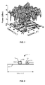
Figure 1 shows a graph presenting an example of variations of magnitudes of a received RF signal at UHF frequency within an indoor area having coordinates X and Y of 2mx2m, respectively. As can be seen on this figure, variations of the RF signal of up to 40 dB could appear over distances of a few tens of centimetres. Such fast fading signal could, disadvantageously, prevent the activation of one RFID tag even for a transmission from a close RFID reader whereas the same tag could be disadvantageously activated by a distant RFID reader increasing the interference issue. A situation may happen in which an RFID tag is located in a so-called fade region with respect to a signal transmitted by a close RFID reader and in a so-called crest region with respect to a signal transmitted by a distant RFID reader. - To mitigate this well-known problem it is possible to use antenna diversity (or spatial diversity) at the reader or the tag side. The use of spatial diversity requires at least two antennas with a minimum of space separation between the two antennas. Typically a quarter wave lambda separation is required in order to insure sufficient decorrelation between the two antennas. This minimum distance between the two antennas is approximately equal to 8 cm at 900 MHz and 17 cm at 433 MHz.
- This minimum distance is not always available in the reader side, in particular when the reader is integrated into mobile devices such as a smartphone or a tablet. The required space for antenna diversity is even less available in the tag side and many objects to be tagged are sized to receive only one single small antenna.
- A purpose of the present invention is to mitigate the RFID range limitation and interferences issues due to multipath frequency fading experienced with long range RFID systems operating in the UHF or microwave RFID bands.
- The use of multi-band radio frequency identification (RFID) device may be seen as an alternative solution to antenna diversity. Frequency diversity is an alternative solution to space diversity, provided that compact and cost effective multi-band frequency tags are available.
- According to an aspect of the invention, there is provided a compact RFID device operating in at least two different frequency bands, for example the 433 MHz band and the 900 MHz band. Compactness may be achieved by using a resonant half-wave dipole coupled to two RFID modules.
- More specifically, a first aspect of the invention relates to a device comprising at least a first RFID module and a second RFID module, each of said at least first and second RFID modules comprising a chip coupled to a wire loop antenna wherein the first and second RFID modules operate at a first operating frequency in a first frequency band and at a second operating frequency in a second frequency band respectively, the second operating frequency being substantially equal to a multiple k of the first operating frequency, with k≥2. The device further comprises a resonant half-wave dipole having a length that is substantially equal to λ/2 where λ is a wavelength associated with the first frequency band, the first and second modules being present along the resonant half-wave dipole in order that the wire loop antenna of said first and second modules is magnetically coupled to the resonant half-wave dipole. The first module is present in the vicinity of the centre of the resonant half-wave dipole and the second module is present at a distance substantially equal to (2*n+1)λ/(4*k) from an end of the resonant half-wave dipole, with n∈[0...k-1].
- According to an embodiment, the resonant half-wave dipole is a conductive rectilinear strip.
- According to another embodiment, the resonant half-wave dipole is a conductive meander strip.
- According to a particular embodiment, the first and second RFID modules are arranged on the same side of the resonant half-wave dipole.
- According to another embodiment, the first and second RFID modules are arranged on opposite sides of the resonant half-wave dipole.
- According to another embodiment, the device further comprises a third RFID module present along the resonant half-wave dipole and operating at a third operating frequency in a third frequency band, said third frequency being substantially equal to a multiple k' of the first operating frequency, with k' ≠ k and k'≥2, and wherein the second module is present at a distance substantially equal to (2*n+1)λ/(4*k') from an end of the resonant half-wave dipole, with n∈[0...k'-1]. In this embodiment, the RFID device operates in three frequency bands.
- It will be appreciated that, the invention may be applied to RFID devices operating in more than three frequency bands.
- According to another embodiment, the RFID device further comprises a fourth RFID module present along the resonant half-wave dipole and operating at a fourth operating frequency in the second frequency band, said fourth frequency being different from the second operating frequency but being substantially equal to the multiple k of the first operating frequency. In this embodiment, the second RFID module and the fourth RFID module are present at a distance substantially equal to (2*n+1)λ/(4*k) and (2*n'+1)λ/(4*k) from an end of the resonant half-wave dipole, with n,n'∈[0... k-1] and n'≠ n. In this embodiment, the RFID device operates in two distinctive frequency bands and more specifically at one operating frequency (the first operating frequency) in the first frequency band and at two operating frequencies (the second and fourth operating frequencies) in the second frequency band.
- Another aspect of the invention relates to radio frequency identification device operating at a plurality of frequency bands comprising
a resonant half wave dipole having a fundamental frequency mode of the lowest frequency band, and
a plurality of loop antennas magnetically coupled to the dipole, the plurality of loop antennas comprising a loop antenna operating at the fundamental frequency mode and at least one loop antenna operating at a harmonic frequency mode, each loop being arranged around a plane of maximum current of the resonant harmonic frequency mode - The invention can be better understood with reference to the following description and drawings, given by way of example and not limiting the scope of protection, and in which:
-
Figure 1 is a chart illustrating the indoor multipath fading effect at 900 MHz; -
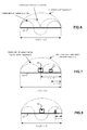
Figure 2 is a first schematic view illustrating a first embodiment of the invention; -
Figure 3 is a schematic view showing the spatial position of the RFID modules of the first embodiment of the invention; -
Figure 4 illustrates the current, voltage and magnetic field distributions along a half-wave dipole; -
Figure 5 illustrates the optimal position of a first RFID module along the half-wave dipole ofFigure 4 ; -
Figure 6 illustrate the current distribution along a half-wave dipole at a fundamental frequency and at two harmonic frequencies; -
Figure 7 illustrate the position of two RFID modules operating at a fundamental frequency f1 and a first harmonic frequency f2 respectively; -
Figure 8 illustrate the position of two RFID modules operating at a fundamental frequency f1 and a second harmonic frequency f3 respectively; -
Figures 9 to 11 illustrate different possible shapes of the half-wave dipole; -
Figure 12 illustrate a first variant of the RFID device according to the invention; -
Figure 13 illustrate a second variant of the RFID device according to the invention; and -
Figure 14 illustrate a third variant of the RFID device according to the invention. - While example embodiments are capable of various modifications and alternative forms, embodiments thereof are shown by way of example in the drawings and will herein be described in details. It should be understood, however, that there is no intent to limit example embodiments to the particular forms disclosed, but on the contrary, example embodiments are to cover all modifications, equivalents, and alternatives falling within the scope of the claims. Like numbers refer to like elements throughout the description of the figures.
-
Figures 2 and3 schematically depict a dual-band RFID device according to a first embodiment of the invention. - The
RFID device 1 comprises two RFID modules or wire loop tags 10 and 11. Each of these RFID modules comprises a chip coupled to a wire loop antenna. More specifically, themodule 10 comprises achip 100 and awire loop antenna 101 while themodule 11 comprises achip 110 and awire loop antenna 111. - Examples of RFID modules or wire loop tags are adhesive tags, referenced ALN - 9613 SIT, provided by Alien Technology or tags, referenced MuTRAK, provided by Tagsys RFID.
- According to this embodiment of the invention, the
RFID modules module 10 and the 900 MHz band for themodule 11. Of course, other RFID bands may be used as mentioned later in the present specification. TheRFID module 10 operates at a first operating frequency f1 in a first frequency band and theRFID module 11 operates at a second operating frequency fk in a second frequency band. The operating frequency fk is substantially equal to a multiple k of the first operating frequency f1, with k≥2. In the example offigure 2 , k=2. - Preferably, the
device 1 further comprises a resonant half-wave dipole 12 having a length L associated with a wavelength λ associated with the first frequency band. As the operating frequency f1 is included in the first frequency band, the wavelength λ is close or equal to the wavelength λ1 associated with the first operating frequency f1. So L=λ/2≈λ1/2. - In addition, the
modules wave dipole 12 in order that their wire loop antennas are each placed around a short circuit plane (i.e. a plan of a maximum of current) of the resonant mode of the half-wave dipole 12. This condition is met when themodule 10 is present in the vicinity of the centre of the resonant half-wave dipole 12 and when themodule 11 is present at a distance substantially equal to (2*n+1)λ/(4*k) from an end of the resonant half-wave dipole 12, with n∈[0...k-1]. - The
module 10 is thus arranged at a distance L1≈L/2=λ/4 from an end of the resonant half-wave dipole 12. And if k=2, as illustrated byfigures 2 and3 , themodule 11 may be arranged at a distance L2≈λ/8 or 3λ/8 from an end of resonant half-wave dipole 12. - The involved phenomenon and the operation of the
RFID device 1 ofFigure 2 will be explained in detail in the following paragraphs. -
Figure 4 shows current and voltage distributions along the half-wave dipole 12 as well as the corresponding magnetic field. The magnetic field is maximum at the middle of the dipole (λ1/4) and minimum at the edges. The magnetic field is shown by a dashed line the thickness of which is depending on the magnitude of the magnetic field. Therefore, for the fundamental mode of the half-wave dipole, the optimum magnetic coupling to the wire loop of a RFID module is obtained at the centre of the dipole. So theRFID module 10 operating at the frequency f1 is arranged at the middle of the half-wave dipole 12 as illustrated inFigure 5 . - The optimum coupling may be adjusted by adjusting the relative distance between the
wire loop antenna 101 and the half-wave dipole 12 and/or by slightly moving thewire loop antenna 101 around the centre of the half-wave dipole 12. - In addition, the present invention takes advantage of the fact that the frequency bands allowed for long range RFID systems are almost multiple of each other. That is, a half wave dipole antenna of length L=λ/2≈λ1/2 at a frequency f1=433 MHz (resp. f3= 2.4 GHz) has substantially a length of λ2 at a frequency f2= 900 MHz (resp. f4=5 GHz). Likewise, a half wave dipole antenna of length L'=λ2/2 at frequency f2=900 MHz has a length of approximately 3xλ3/2 at the frequency of f3= 2.4 GHz.
-
Figure 6 shows the current distribution of a half-wave dipole at the fundamental mode (frequency f1) and at the two first harmonic modes (frequencies f2=2xf1 and f3=3xf1). - As illustrated in
Figure 7 , the principle of the invention is to use a resonant half-wave dipole at the fundamental mode corresponding to the lowest frequency band (e.g. 433 MHz band), magnetically coupled to several miniature wire-loop tags or RFID modules (2 in the case offigure 7 ) operating at the fundamental (i.e. 433 MHz band) or the harmonic frequency bands (e.g. 900 MHz band). For efficient coupling of theRFID modules wave dipole 12 at the different frequencies, each RFID module is placed around a short circuit plane (i.e. a plan of a maximum of current) of the corresponding resonant mode of the half-wave dipole 12. In the example ofFigure 7 , themodule 10 is placed at a distance L1=L/2≈λ/4 from the right end of thedipole 12 and themodule 11 is placed at a distance L2=L/4≈λ/8 from the right end of thedipole 12. -
Figures 1 to 7 have illustrated a dual-band RFID device operating at a fundamental frequency f1 into a first frequency band (e.g. 433 MHz band or 2.4 GHz band) and a first harmonic frequency f2 into a second frequency band (e.g. 900 MHz band or 5 GHz band). The frequencies f1 and f2 are for example the following ones: f1=433 MHz and f2=866 MHz or f1=2.45 GHz and f2=5 GHz. -
Figure 8 shows another example of dual-band RFID device operating at a fundamental frequency (f1) and a third harmonic frequency (f3= 3xf1). TheRFID module 10 is placed at the middle of the half-wave dipole 12 and theRFID module 11 is arranged substantially at a length L3=L/6=λ/12 from the right end of the half-wave dipole. Themodule 11 could also be placed at a length of 3λ/12 or 5λ/12 from the right end of the half-wave dipole. - An RFID device in accordance with described embodiments provides the following advantages:
- it provides a compact and cost effective dual band RFID device since the two RFID modules are coupled to a same resonant half-wave dipole; and
- this solution uses Commercial Off The Shelf (COTS) RFID modules or tags as those provided by Tagsys or Alien Technology
- The above-described RFID comprises two
RFID modules rectilinear strip 12 used as a resonant half-wave dipole and the two RFID modules are arranged on the same side of the resonant half-wave dipole 12. - Different variants are possible. In a first variant, other shapes of half-wave dipole can be used. In
figures 9 to 11 , the resonant half-wave dipole 12 is a conductive meander strip. The shape of the half wave dipole can adapted in order to match the form factor and the size of the available space of the object to be tagged with RFID device. - In another variant illustrated by
figure 12 , theRFID modules wave dipole 12. - In another variant, the wire-
loop antenna Figures 2-12 . - In addition, the dual-band RFID device according to invention can also comprise an
additional RFID module 13 present along the resonant half-wave dipole 12 and operating at the operating frequency f2 or at an operating frequency f2, in the second frequency band as illustrated byFigure 13 . In this figure, theRFID module 11 is arranged at a distance L2=L/4=λ/8 from the right end of the half-wave dipole 12 and theRFID module 13 is arranged at a distance L2'=3L/4=3λ/8 from the right end of the half-wave dipole 12. The twomodules - In this variant, as a general rule, the
RFID module 11 operating at the operating frequency fk is arranged at a distance substantially equal to (2*n+1)λ/(4*k) from an end of the half-wave dipole 12, with n∈[0...k-1], and theRFID module 13 operating at the operating frequency fk, is arranged at a distance substantially equal to (2*n'+1)λ/(4*k) from the above mentioned end of the half-wave dipole 12, with n'∈[0...k-1] and n'≠ n. - In another variant illustrated by
Figure 14 , the RFID device operates in three frequency bands, for example the 433 MHz band, the 900 MHz band and the 2.4 GHz band. The device comprises aRFID module 10 operating at the operating frequency f1, aRFID module 11 operating at the operating frequency f2 ≈ 2xf1 and aRFID module 13 operating at the operating frequency f3 ≈ 3xf2=6xf1 The RFID modules are placed around a short circuit plane (maximum current) associated to their operating frequency along the half-wave dipole 12. - In
figure 14 , theRFID module wave dipole 12. - In this variant, as a general rule, the
RFID module 13 operating at the operating frequency fk is arranged at a distance substantially equal to (2*n+1)λ/(4*k) from an end of the half-wave dipole 12, with n∈[0...k-1],
Claims (7)
- Device comprising a first radio frequency identification module (10) and a second radio frequency identification module (11), each of said first and second radio frequency identification modules comprising a chip (100,110) coupled to a wire loop antenna (101,111),
wherein the first and second radio frequency identification modules (10,11) operate at a first operating frequency (f1) in a first frequency band and at a second operating frequency (fk) in a second frequency band respectively, the second operating frequency (fk) being substantially equal to a multiple k of the first operating frequency (f1), with k≥2,
wherein the device further comprises a resonant half-wave dipole (12) having a length (L) that is substantially equal to λ/2 where λ is a wavelength associated with the first frequency band, the first and second modules being present along the resonant half-wave dipole (12) such that the wire loop antenna of said first and second modules is magnetically coupled to the resonant half-wave dipole (12), and
wherein the first module is present in the vicinity of the centre of the resonant half-wave dipole (12) and the second module is present at a distance substantially equal to (2*n+1)λ/(4*k) from an end of the resonant half-wave dipole (12), with n∈[0...k-1]. - Device according to claim 1, wherein the resonant half-wave dipole (12) is a conductive rectilinear strip.
- Device according to claim 1, wherein the resonant half-wave dipole (12) is a conductive meander strip.
- Device according to any one of claims 1 to 3, wherein the first and second radio frequency identification modules are arranged on the same side of the resonant half-wave dipole (12).
- Device according to any one of claims 1 to 3, wherein the first and second radio frequency identification modules are arranged on opposite sides of the resonant half-wave dipole (12).
- Device according to any one of claims 1 to 5, further comprising a third radio frequency identification module (13) present along the resonant half-wave dipole (12) and operating at a third operating frequency (fk') in a third frequency band, said third frequency being substantially equal to a multiple k' of the first operating frequency (f1), with k'≠ k and k'≥2, and wherein the second module is present at a distance substantially equal to (2*n+1)λ/(4*k') from an end of the resonant half-wave dipole (12), with n∈[0...k'-1].
- Device according to any one of claims 1 to 6, further comprising a fourth radio frequency identification module (13) present along the resonant half-wave dipole (12) and operating at a fourth operating frequency (fk') in the second frequency band, said fourth frequency being different from the second operating frequency (fk) but being substantially equal to the multiple k of the first operating frequency (f1), and wherein the second radio frequency identification module and the fourth radio frequency identification module are present at a distance substantially equal to (2*n+1)λ/(4*k) and (2*n'+1)λ/(4*k) from an end of the resonant half-wave dipole (12), with n, n'∈[0...k-1] and n'≠ n.
Priority Applications (2)
| Application Number | Priority Date | Filing Date | Title |
|---|---|---|---|
| EP15306709.5A EP3163511B1 (en) | 2015-10-26 | 2015-10-26 | Multi-band rfid device |
| US15/333,480 US10038233B2 (en) | 2015-10-26 | 2016-10-25 | Multi-band RFID device |
Applications Claiming Priority (1)
| Application Number | Priority Date | Filing Date | Title |
|---|---|---|---|
| EP15306709.5A EP3163511B1 (en) | 2015-10-26 | 2015-10-26 | Multi-band rfid device |
Publications (2)
| Publication Number | Publication Date |
|---|---|
| EP3163511A1 true EP3163511A1 (en) | 2017-05-03 |
| EP3163511B1 EP3163511B1 (en) | 2018-08-22 |
Family
ID=54396805
Family Applications (1)
| Application Number | Title | Priority Date | Filing Date |
|---|---|---|---|
| EP15306709.5A Not-in-force EP3163511B1 (en) | 2015-10-26 | 2015-10-26 | Multi-band rfid device |
Country Status (2)
| Country | Link |
|---|---|
| US (1) | US10038233B2 (en) |
| EP (1) | EP3163511B1 (en) |
Families Citing this family (5)
| Publication number | Priority date | Publication date | Assignee | Title |
|---|---|---|---|---|
| CN108460445A (en) * | 2018-05-30 | 2018-08-28 | 云南电网有限责任公司带电作业分公司 | A kind of highly sensitive RFID tag of anti-strong-electromagnetic field |
| CN111967563B (en) * | 2020-09-04 | 2022-02-18 | 浙江大学 | Combined ultra-wideband cross-polarization chipless RFID tag based on MFCC feature coding |
| JP7733752B2 (en) * | 2021-06-24 | 2025-09-03 | エイヴェリー デニソン リテール インフォメーション サービシズ リミテッド ライアビリティ カンパニー | Microwave-resistant RFID systems and components |
| JP2023115681A (en) * | 2022-02-08 | 2023-08-21 | サトーホールディングス株式会社 | Antenna pattern, RFID inlay |
| CN119029550B (en) * | 2024-10-29 | 2025-01-03 | 广东盛华德通讯科技股份有限公司 | A high frequency antenna system and working method thereof |
Citations (2)
| Publication number | Priority date | Publication date | Assignee | Title |
|---|---|---|---|---|
| US20110285511A1 (en) * | 2009-06-12 | 2011-11-24 | Impinji, Inc. | Dual-frequency rfid tag with isolated inputs |
| US20120249306A1 (en) * | 2011-03-31 | 2012-10-04 | Fujifilm Corporation | Rf-id tag and rf-id communication system |
Family Cites Families (8)
| Publication number | Priority date | Publication date | Assignee | Title |
|---|---|---|---|---|
| US7589675B2 (en) | 2006-05-19 | 2009-09-15 | Industrial Technology Research Institute | Broadband antenna |
| JP2008041005A (en) | 2006-08-10 | 2008-02-21 | Hitachi Ltd | RFID tag and manufacturing method thereof |
| JP4671001B2 (en) * | 2008-07-04 | 2011-04-13 | 株式会社村田製作所 | Wireless IC device |
| TWI382595B (en) * | 2008-09-16 | 2013-01-11 | Polychem Uv Eb Internat Corp | Antenna construction of RFID transponder and its manufacturing method |
| CN102422310B (en) | 2009-03-10 | 2015-11-25 | 沃尔玛百货有限公司 | General RFID label and method of manufacture |
| GB2487315B (en) * | 2009-11-04 | 2014-09-24 | Murata Manufacturing Co | Communication terminal and information processing system |
| KR20110057325A (en) | 2009-11-24 | 2011-06-01 | 주식회사 이엠따블유 | Handheld terminal with RFID tag |
| JP2012108843A (en) | 2010-11-19 | 2012-06-07 | Toppan Printing Co Ltd | RFID tag |
-
2015
- 2015-10-26 EP EP15306709.5A patent/EP3163511B1/en not_active Not-in-force
-
2016
- 2016-10-25 US US15/333,480 patent/US10038233B2/en not_active Expired - Fee Related
Patent Citations (2)
| Publication number | Priority date | Publication date | Assignee | Title |
|---|---|---|---|---|
| US20110285511A1 (en) * | 2009-06-12 | 2011-11-24 | Impinji, Inc. | Dual-frequency rfid tag with isolated inputs |
| US20120249306A1 (en) * | 2011-03-31 | 2012-10-04 | Fujifilm Corporation | Rf-id tag and rf-id communication system |
Also Published As
| Publication number | Publication date |
|---|---|
| US20170117607A1 (en) | 2017-04-27 |
| US10038233B2 (en) | 2018-07-31 |
| EP3163511B1 (en) | 2018-08-22 |
Similar Documents
| Publication | Publication Date | Title |
|---|---|---|
| US10325708B2 (en) | Spiral near field communication (NFC) antenna coil | |
| US7154449B2 (en) | Antenna | |
| JP4393228B2 (en) | Small antenna and wireless tag provided with the same | |
| US10038233B2 (en) | Multi-band RFID device | |
| US9460320B2 (en) | Transceiver and radio frequency identification tag reader | |
| KR20140075021A (en) | Miniaturized radio-frequency identification tag and microstrip patch antenna thereof | |
| US20080143620A1 (en) | Increasing the bandwidth of a RFID dipole tag | |
| EP2345983B1 (en) | Radio frequency identification tag | |
| US20160156110A1 (en) | Antenna isolator | |
| CN103985958B (en) | Small metal resistance type UHF tag antenna based on EBG structure | |
| EP2779305B1 (en) | Multi-Loop Antenna System for Contactless Applications | |
| CN202121074U (en) | Antenna for radio frequency identification devices (RFID) readers and RFID reader | |
| Faudzi et al. | A compact dipole UHF-RFID tag antenna | |
| CN109216916A (en) | A kind of 5G antenna element, aerial array and antenna system | |
| KR102146020B1 (en) | Soft magnetic substrate, wireless communication device and wireless power conversion device | |
| KR20140119534A (en) | Rfid tag applying conductive loop | |
| KR100867853B1 (en) | RFID antennas and RDF tags | |
| Catarinucci et al. | Platform-robust passive UHF RFID tags: A case-study in robotics | |
| KR100862477B1 (en) | RFID tag | |
| Wang et al. | A UHF RFID reader antenna with near field inductive wireless power transfer feature | |
| Choudhary et al. | Platform Insensitive, Compact Flippable Near Field UHF RFID Tag, Compliant with ETSI/FCC bands | |
| KR20080065405A (en) | RFID tag | |
| Evizal et al. | A multi band mini printed omni directional antenna with V-shaped for RFID applications | |
| Dufek et al. | Adaptation of an active RFID technology for low power wireless sensor networks | |
| Deleruyelle et al. | Multistandard UHF and UWB tag antenna for RFID and positioning applications |
Legal Events
| Date | Code | Title | Description |
|---|---|---|---|
| PUAI | Public reference made under article 153(3) epc to a published international application that has entered the european phase |
Free format text: ORIGINAL CODE: 0009012 |
|
| AK | Designated contracting states |
Kind code of ref document: A1 Designated state(s): AL AT BE BG CH CY CZ DE DK EE ES FI FR GB GR HR HU IE IS IT LI LT LU LV MC MK MT NL NO PL PT RO RS SE SI SK SM TR |
|
| AX | Request for extension of the european patent |
Extension state: BA ME |
|
| 17P | Request for examination filed |
Effective date: 20171025 |
|
| RBV | Designated contracting states (corrected) |
Designated state(s): AL AT BE BG CH CY CZ DE DK EE ES FI FR GB GR HR HU IE IS IT LI LT LU LV MC MK MT NL NO PL PT RO RS SE SI SK SM TR |
|
| REG | Reference to a national code |
Ref country code: DE Ref legal event code: R079 Ref document number: 602015015059 Country of ref document: DE Free format text: PREVIOUS MAIN CLASS: G06K0019077000 Ipc: H01Q0001220000 |
|
| GRAP | Despatch of communication of intention to grant a patent |
Free format text: ORIGINAL CODE: EPIDOSNIGR1 |
|
| RIC1 | Information provided on ipc code assigned before grant |
Ipc: G06K 19/07 20060101ALI20180220BHEP Ipc: H01Q 1/22 20060101AFI20180220BHEP Ipc: H01Q 9/06 20060101ALI20180220BHEP Ipc: G06K 19/077 20060101ALI20180220BHEP Ipc: H01Q 5/50 20150101ALI20180220BHEP |
|
| INTG | Intention to grant announced |
Effective date: 20180308 |
|
| GRAS | Grant fee paid |
Free format text: ORIGINAL CODE: EPIDOSNIGR3 |
|
| GRAA | (expected) grant |
Free format text: ORIGINAL CODE: 0009210 |
|
| AK | Designated contracting states |
Kind code of ref document: B1 Designated state(s): AL AT BE BG CH CY CZ DE DK EE ES FI FR GB GR HR HU IE IS IT LI LT LU LV MC MK MT NL NO PL PT RO RS SE SI SK SM TR |
|
| REG | Reference to a national code |
Ref country code: GB Ref legal event code: FG4D |
|
| REG | Reference to a national code |
Ref country code: CH Ref legal event code: EP |
|
| REG | Reference to a national code |
Ref country code: AT Ref legal event code: REF Ref document number: 1033530 Country of ref document: AT Kind code of ref document: T Effective date: 20180915 |
|
| REG | Reference to a national code |
Ref country code: IE Ref legal event code: FG4D |
|
| REG | Reference to a national code |
Ref country code: DE Ref legal event code: R096 Ref document number: 602015015059 Country of ref document: DE |
|
| REG | Reference to a national code |
Ref country code: NL Ref legal event code: MP Effective date: 20180822 |
|
| REG | Reference to a national code |
Ref country code: LT Ref legal event code: MG4D |
|
| PG25 | Lapsed in a contracting state [announced via postgrant information from national office to epo] |
Ref country code: FI Free format text: LAPSE BECAUSE OF FAILURE TO SUBMIT A TRANSLATION OF THE DESCRIPTION OR TO PAY THE FEE WITHIN THE PRESCRIBED TIME-LIMIT Effective date: 20180822 Ref country code: SE Free format text: LAPSE BECAUSE OF FAILURE TO SUBMIT A TRANSLATION OF THE DESCRIPTION OR TO PAY THE FEE WITHIN THE PRESCRIBED TIME-LIMIT Effective date: 20180822 Ref country code: BG Free format text: LAPSE BECAUSE OF FAILURE TO SUBMIT A TRANSLATION OF THE DESCRIPTION OR TO PAY THE FEE WITHIN THE PRESCRIBED TIME-LIMIT Effective date: 20181122 Ref country code: NL Free format text: LAPSE BECAUSE OF FAILURE TO SUBMIT A TRANSLATION OF THE DESCRIPTION OR TO PAY THE FEE WITHIN THE PRESCRIBED TIME-LIMIT Effective date: 20180822 Ref country code: RS Free format text: LAPSE BECAUSE OF FAILURE TO SUBMIT A TRANSLATION OF THE DESCRIPTION OR TO PAY THE FEE WITHIN THE PRESCRIBED TIME-LIMIT Effective date: 20180822 Ref country code: IS Free format text: LAPSE BECAUSE OF FAILURE TO SUBMIT A TRANSLATION OF THE DESCRIPTION OR TO PAY THE FEE WITHIN THE PRESCRIBED TIME-LIMIT Effective date: 20181222 Ref country code: GR Free format text: LAPSE BECAUSE OF FAILURE TO SUBMIT A TRANSLATION OF THE DESCRIPTION OR TO PAY THE FEE WITHIN THE PRESCRIBED TIME-LIMIT Effective date: 20181123 Ref country code: NO Free format text: LAPSE BECAUSE OF FAILURE TO SUBMIT A TRANSLATION OF THE DESCRIPTION OR TO PAY THE FEE WITHIN THE PRESCRIBED TIME-LIMIT Effective date: 20181122 Ref country code: LT Free format text: LAPSE BECAUSE OF FAILURE TO SUBMIT A TRANSLATION OF THE DESCRIPTION OR TO PAY THE FEE WITHIN THE PRESCRIBED TIME-LIMIT Effective date: 20180822 |
|
| REG | Reference to a national code |
Ref country code: AT Ref legal event code: MK05 Ref document number: 1033530 Country of ref document: AT Kind code of ref document: T Effective date: 20180822 |
|
| PG25 | Lapsed in a contracting state [announced via postgrant information from national office to epo] |
Ref country code: HR Free format text: LAPSE BECAUSE OF FAILURE TO SUBMIT A TRANSLATION OF THE DESCRIPTION OR TO PAY THE FEE WITHIN THE PRESCRIBED TIME-LIMIT Effective date: 20180822 Ref country code: LV Free format text: LAPSE BECAUSE OF FAILURE TO SUBMIT A TRANSLATION OF THE DESCRIPTION OR TO PAY THE FEE WITHIN THE PRESCRIBED TIME-LIMIT Effective date: 20180822 Ref country code: AL Free format text: LAPSE BECAUSE OF FAILURE TO SUBMIT A TRANSLATION OF THE DESCRIPTION OR TO PAY THE FEE WITHIN THE PRESCRIBED TIME-LIMIT Effective date: 20180822 |
|
| PG25 | Lapsed in a contracting state [announced via postgrant information from national office to epo] |
Ref country code: ES Free format text: LAPSE BECAUSE OF FAILURE TO SUBMIT A TRANSLATION OF THE DESCRIPTION OR TO PAY THE FEE WITHIN THE PRESCRIBED TIME-LIMIT Effective date: 20180822 Ref country code: AT Free format text: LAPSE BECAUSE OF FAILURE TO SUBMIT A TRANSLATION OF THE DESCRIPTION OR TO PAY THE FEE WITHIN THE PRESCRIBED TIME-LIMIT Effective date: 20180822 Ref country code: CZ Free format text: LAPSE BECAUSE OF FAILURE TO SUBMIT A TRANSLATION OF THE DESCRIPTION OR TO PAY THE FEE WITHIN THE PRESCRIBED TIME-LIMIT Effective date: 20180822 Ref country code: RO Free format text: LAPSE BECAUSE OF FAILURE TO SUBMIT A TRANSLATION OF THE DESCRIPTION OR TO PAY THE FEE WITHIN THE PRESCRIBED TIME-LIMIT Effective date: 20180822 Ref country code: EE Free format text: LAPSE BECAUSE OF FAILURE TO SUBMIT A TRANSLATION OF THE DESCRIPTION OR TO PAY THE FEE WITHIN THE PRESCRIBED TIME-LIMIT Effective date: 20180822 Ref country code: IT Free format text: LAPSE BECAUSE OF FAILURE TO SUBMIT A TRANSLATION OF THE DESCRIPTION OR TO PAY THE FEE WITHIN THE PRESCRIBED TIME-LIMIT Effective date: 20180822 Ref country code: PL Free format text: LAPSE BECAUSE OF FAILURE TO SUBMIT A TRANSLATION OF THE DESCRIPTION OR TO PAY THE FEE WITHIN THE PRESCRIBED TIME-LIMIT Effective date: 20180822 |
|
| REG | Reference to a national code |
Ref country code: DE Ref legal event code: R119 Ref document number: 602015015059 Country of ref document: DE |
|
| PG25 | Lapsed in a contracting state [announced via postgrant information from national office to epo] |
Ref country code: DK Free format text: LAPSE BECAUSE OF FAILURE TO SUBMIT A TRANSLATION OF THE DESCRIPTION OR TO PAY THE FEE WITHIN THE PRESCRIBED TIME-LIMIT Effective date: 20180822 Ref country code: SM Free format text: LAPSE BECAUSE OF FAILURE TO SUBMIT A TRANSLATION OF THE DESCRIPTION OR TO PAY THE FEE WITHIN THE PRESCRIBED TIME-LIMIT Effective date: 20180822 Ref country code: SK Free format text: LAPSE BECAUSE OF FAILURE TO SUBMIT A TRANSLATION OF THE DESCRIPTION OR TO PAY THE FEE WITHIN THE PRESCRIBED TIME-LIMIT Effective date: 20180822 |
|
| REG | Reference to a national code |
Ref country code: CH Ref legal event code: PL |
|
| REG | Reference to a national code |
Ref country code: BE Ref legal event code: MM Effective date: 20181031 |
|
| PG25 | Lapsed in a contracting state [announced via postgrant information from national office to epo] |
Ref country code: LU Free format text: LAPSE BECAUSE OF NON-PAYMENT OF DUE FEES Effective date: 20181026 Ref country code: MC Free format text: LAPSE BECAUSE OF FAILURE TO SUBMIT A TRANSLATION OF THE DESCRIPTION OR TO PAY THE FEE WITHIN THE PRESCRIBED TIME-LIMIT Effective date: 20180822 |
|
| PLBE | No opposition filed within time limit |
Free format text: ORIGINAL CODE: 0009261 |
|
| STAA | Information on the status of an ep patent application or granted ep patent |
Free format text: STATUS: NO OPPOSITION FILED WITHIN TIME LIMIT |
|
| REG | Reference to a national code |
Ref country code: IE Ref legal event code: MM4A |
|
| 26N | No opposition filed |
Effective date: 20190523 |
|
| PG25 | Lapsed in a contracting state [announced via postgrant information from national office to epo] |
Ref country code: DE Free format text: LAPSE BECAUSE OF NON-PAYMENT OF DUE FEES Effective date: 20190501 |
|
| PG25 | Lapsed in a contracting state [announced via postgrant information from national office to epo] |
Ref country code: BE Free format text: LAPSE BECAUSE OF NON-PAYMENT OF DUE FEES Effective date: 20181031 Ref country code: CH Free format text: LAPSE BECAUSE OF NON-PAYMENT OF DUE FEES Effective date: 20181031 Ref country code: SI Free format text: LAPSE BECAUSE OF FAILURE TO SUBMIT A TRANSLATION OF THE DESCRIPTION OR TO PAY THE FEE WITHIN THE PRESCRIBED TIME-LIMIT Effective date: 20180822 Ref country code: LI Free format text: LAPSE BECAUSE OF NON-PAYMENT OF DUE FEES Effective date: 20181031 |
|
| PG25 | Lapsed in a contracting state [announced via postgrant information from national office to epo] |
Ref country code: IE Free format text: LAPSE BECAUSE OF NON-PAYMENT OF DUE FEES Effective date: 20181026 Ref country code: FR Free format text: LAPSE BECAUSE OF NON-PAYMENT OF DUE FEES Effective date: 20181031 |
|
| PG25 | Lapsed in a contracting state [announced via postgrant information from national office to epo] |
Ref country code: MT Free format text: LAPSE BECAUSE OF NON-PAYMENT OF DUE FEES Effective date: 20181026 |
|
| PG25 | Lapsed in a contracting state [announced via postgrant information from national office to epo] |
Ref country code: TR Free format text: LAPSE BECAUSE OF FAILURE TO SUBMIT A TRANSLATION OF THE DESCRIPTION OR TO PAY THE FEE WITHIN THE PRESCRIBED TIME-LIMIT Effective date: 20180822 |
|
| PG25 | Lapsed in a contracting state [announced via postgrant information from national office to epo] |
Ref country code: PT Free format text: LAPSE BECAUSE OF FAILURE TO SUBMIT A TRANSLATION OF THE DESCRIPTION OR TO PAY THE FEE WITHIN THE PRESCRIBED TIME-LIMIT Effective date: 20180822 |
|
| PG25 | Lapsed in a contracting state [announced via postgrant information from national office to epo] |
Ref country code: HU Free format text: LAPSE BECAUSE OF FAILURE TO SUBMIT A TRANSLATION OF THE DESCRIPTION OR TO PAY THE FEE WITHIN THE PRESCRIBED TIME-LIMIT; INVALID AB INITIO Effective date: 20151026 Ref country code: CY Free format text: LAPSE BECAUSE OF FAILURE TO SUBMIT A TRANSLATION OF THE DESCRIPTION OR TO PAY THE FEE WITHIN THE PRESCRIBED TIME-LIMIT Effective date: 20180822 Ref country code: MK Free format text: LAPSE BECAUSE OF NON-PAYMENT OF DUE FEES Effective date: 20180822 |
|
| GBPC | Gb: european patent ceased through non-payment of renewal fee |
Effective date: 20191026 |
|
| PG25 | Lapsed in a contracting state [announced via postgrant information from national office to epo] |
Ref country code: GB Free format text: LAPSE BECAUSE OF NON-PAYMENT OF DUE FEES Effective date: 20191026 |