EP3160005A1 - Power adapter - Google Patents
Power adapter Download PDFInfo
- Publication number
- EP3160005A1 EP3160005A1 EP16761041.9A EP16761041A EP3160005A1 EP 3160005 A1 EP3160005 A1 EP 3160005A1 EP 16761041 A EP16761041 A EP 16761041A EP 3160005 A1 EP3160005 A1 EP 3160005A1
- Authority
- EP
- European Patent Office
- Prior art keywords
- voltage
- output port
- processor
- voltage divider
- power adapter
- Prior art date
- Legal status (The legal status is an assumption and is not a legal conclusion. Google has not performed a legal analysis and makes no representation as to the accuracy of the status listed.)
- Ceased
Links
Images

Classifications
-
- H—ELECTRICITY
- H02—GENERATION; CONVERSION OR DISTRIBUTION OF ELECTRIC POWER
- H02J—ELECTRIC POWER NETWORKS; CIRCUIT ARRANGEMENTS OR SYSTEMS FOR SUPPLYING OR DISTRIBUTING ELECTRIC POWER; SYSTEMS FOR STORING ELECTRIC ENERGY
- H02J7/00—Circuit arrangements for charging or discharging batteries or for supplying loads from batteries
- H02J7/02—Circuit arrangements for charging or discharging batteries or for supplying loads from batteries for charging batteries from AC mains by converters
- H02J7/04—Regulation of charging current or voltage
-
- H—ELECTRICITY
- H02—GENERATION; CONVERSION OR DISTRIBUTION OF ELECTRIC POWER
- H02M—APPARATUS FOR CONVERSION BETWEEN AC AND AC, BETWEEN AC AND DC, OR BETWEEN DC AND DC, AND FOR USE WITH MAINS OR SIMILAR POWER SUPPLY SYSTEMS; CONVERSION OF DC OR AC INPUT POWER INTO SURGE OUTPUT POWER; CONTROL OR REGULATION THEREOF
- H02M7/00—Conversion of AC power input into DC power output; Conversion of DC power input into AC power output
- H02M7/02—Conversion of AC power input into DC power output without possibility of reversal
- H02M7/04—Conversion of AC power input into DC power output without possibility of reversal by static converters
- H02M7/12—Conversion of AC power input into DC power output without possibility of reversal by static converters using discharge tubes with control electrode or semiconductor devices with control electrode
- H02M7/21—Conversion of AC power input into DC power output without possibility of reversal by static converters using discharge tubes with control electrode or semiconductor devices with control electrode using devices of a triode or transistor type requiring continuous application of a control signal
- H02M7/217—Conversion of AC power input into DC power output without possibility of reversal by static converters using discharge tubes with control electrode or semiconductor devices with control electrode using devices of a triode or transistor type requiring continuous application of a control signal using semiconductor devices only
-
- H—ELECTRICITY
- H02—GENERATION; CONVERSION OR DISTRIBUTION OF ELECTRIC POWER
- H02J—ELECTRIC POWER NETWORKS; CIRCUIT ARRANGEMENTS OR SYSTEMS FOR SUPPLYING OR DISTRIBUTING ELECTRIC POWER; SYSTEMS FOR STORING ELECTRIC ENERGY
- H02J7/00—Circuit arrangements for charging or discharging batteries or for supplying loads from batteries
- H02J7/60—Circuit arrangements for charging or discharging batteries or for supplying loads from batteries including safety or protection arrangements
- H02J7/64—Circuit arrangements for charging or discharging batteries or for supplying loads from batteries including safety or protection arrangements against overvoltage
-
- H—ELECTRICITY
- H02—GENERATION; CONVERSION OR DISTRIBUTION OF ELECTRIC POWER
- H02J—ELECTRIC POWER NETWORKS; CIRCUIT ARRANGEMENTS OR SYSTEMS FOR SUPPLYING OR DISTRIBUTING ELECTRIC POWER; SYSTEMS FOR STORING ELECTRIC ENERGY
- H02J7/00—Circuit arrangements for charging or discharging batteries or for supplying loads from batteries
- H02J7/90—Regulation of charging or discharging current or voltage
-
- H—ELECTRICITY
- H02—GENERATION; CONVERSION OR DISTRIBUTION OF ELECTRIC POWER
- H02M—APPARATUS FOR CONVERSION BETWEEN AC AND AC, BETWEEN AC AND DC, OR BETWEEN DC AND DC, AND FOR USE WITH MAINS OR SIMILAR POWER SUPPLY SYSTEMS; CONVERSION OF DC OR AC INPUT POWER INTO SURGE OUTPUT POWER; CONTROL OR REGULATION THEREOF
- H02M1/00—Details of apparatus for conversion
- H02M1/32—Means for protecting converters other than automatic disconnection
-
- H—ELECTRICITY
- H02—GENERATION; CONVERSION OR DISTRIBUTION OF ELECTRIC POWER
- H02M—APPARATUS FOR CONVERSION BETWEEN AC AND AC, BETWEEN AC AND DC, OR BETWEEN DC AND DC, AND FOR USE WITH MAINS OR SIMILAR POWER SUPPLY SYSTEMS; CONVERSION OF DC OR AC INPUT POWER INTO SURGE OUTPUT POWER; CONTROL OR REGULATION THEREOF
- H02M7/00—Conversion of AC power input into DC power output; Conversion of DC power input into AC power output
- H02M7/02—Conversion of AC power input into DC power output without possibility of reversal
- H02M7/04—Conversion of AC power input into DC power output without possibility of reversal by static converters
-
- H—ELECTRICITY
- H02—GENERATION; CONVERSION OR DISTRIBUTION OF ELECTRIC POWER
- H02H—EMERGENCY PROTECTIVE CIRCUIT ARRANGEMENTS
- H02H9/00—Emergency protective circuit arrangements for limiting excess current or voltage without disconnection
- H02H9/04—Emergency protective circuit arrangements for limiting excess current or voltage without disconnection responsive to excess voltage
- H02H9/041—Emergency protective circuit arrangements for limiting excess current or voltage without disconnection responsive to excess voltage using a short-circuiting device
-
- H—ELECTRICITY
- H02—GENERATION; CONVERSION OR DISTRIBUTION OF ELECTRIC POWER
- H02J—ELECTRIC POWER NETWORKS; CIRCUIT ARRANGEMENTS OR SYSTEMS FOR SUPPLYING OR DISTRIBUTING ELECTRIC POWER; SYSTEMS FOR STORING ELECTRIC ENERGY
- H02J7/00—Circuit arrangements for charging or discharging batteries or for supplying loads from batteries
- H02J7/60—Circuit arrangements for charging or discharging batteries or for supplying loads from batteries including safety or protection arrangements
- H02J7/62—Circuit arrangements for charging or discharging batteries or for supplying loads from batteries including safety or protection arrangements against overcurrent
-
- H—ELECTRICITY
- H02—GENERATION; CONVERSION OR DISTRIBUTION OF ELECTRIC POWER
- H02M—APPARATUS FOR CONVERSION BETWEEN AC AND AC, BETWEEN AC AND DC, OR BETWEEN DC AND DC, AND FOR USE WITH MAINS OR SIMILAR POWER SUPPLY SYSTEMS; CONVERSION OF DC OR AC INPUT POWER INTO SURGE OUTPUT POWER; CONTROL OR REGULATION THEREOF
- H02M1/00—Details of apparatus for conversion
- H02M1/0045—Converters combining the concepts of switch-mode regulation and linear regulation, e.g. linear pre-regulator to switching converter, linear and switching converter in parallel, same converter or same transistor operating either in linear or switching mode
Definitions
- the present disclosure relates to charging technical field, and more particularly to a power adapter.
- electronic devices e.g., mobile phones
- a rechargeable battery thus the battery can be charged by a power adapter.
- the power adapter converts an alternating current into a direct current having a specified voltage, and transmits the direct current to an electronic device.
- the electronic device includes a charging control circuit configured to control charging of the battery.
- a power adapter is provided, which can improve safety of charging.
- a power adapter configured to acquire an alternating current from a power source and convert the alternating current into a direct current having a specified voltage; an output port comprising a positive output port and a negative output port both electrically coupled to the adapter main body, and configured to acquire the direct current from the adapter main body, and supply the direct current to an external device via the positive output port and the negative output port; a voltage divider arranged between the positive output port and the negative output port, and configured to execute a voltage division operation upon receiving a control signal, so as to cause a value of an output voltage output through the positive output port and the negative output port to be less than or equal to a preset value; and a processor communicating with the voltage divider and configured to transmit the control signal to the voltage divider.
- the power adapter further comprises an input port communicating with the processor, and configured to receive information from the external device and transmit the information to the processor.
- the processor is configured to transmit the control signal to the voltage divider upon receiving information for indicating that the output voltage needs to be reduced from the external device via the input port.
- the power adapter further comprises a voltage sensor communicating with the processor, and configured to detect a voltage value of the direct current and transmit the voltage value to the processor.
- the processor is configured to transmit the control signal to the voltage divider when it is determined that the voltage value is greater than the preset value.
- the processor is further configured to control the voltage division operation executed by the voltage divider according to the voltage value.
- the voltage divider comprises a metal-oxide -semiconductor field effect transistor switch.
- the voltage divider comprises a transistor switch.
- the output port is configured to output the direct current to a mobile phone.
- the voltage output through the positive output port and the negative output port can be reduced to be less than or equal to the preset value, which can avoid damage and burst of the battery, according usage safety is improved.
- FIG. 1 is a diagrammatic view of a power adapter 100 in accordance with an embodiment of the present disclosure. As illustrated by FIG. 1 , the power adapter 100 includes following.
- An adapter main body 110 is configured to acquire an alternating current from a power source, and convert the alternating current into a direct current having a specified voltage.
- An output port 120 includes a positive output port 122 and a negative output port 124 both electrically coupled to the adapter main body 110, and is configured to acquire the direct current from the adapter main body 110, and supply the direct current to an external device via the positive output port 122 and the negative output port 124.
- a voltage divider 130 is arranged between the adapter main body 110 and the output port 120, and is configured to execute a voltage division operation upon receiving a control signal, so as to cause a value of a voltage output through the positive output port 122 and the negative output port 124 to be less than or equal to a preset value.
- a processor 140 communicates with the voltage divider 130, and is configured to transmit the control signal to the voltage divider 130.
- Adapter main body 110 A. Adapter main body 110
- the adapter main body 110 can acquire the alternating current (or, AC voltage or AC current) from the power source, and perform an alternating-direct conversion process on the alternating current to generate the direct current having the specified voltage (for example, less than or equal to 5V).
- a voltage transformation process is performed on the alternating current having the 220V or 110V voltage and input by the grid, so as to acquire the alternating current having the specified voltage (for example, less than or equal to 5V).
- a rectifying filter process is performed on the alternating current after the alternating current undergoes a voltage reduction process, so as to acquire the desired direct current.
- the adapter main body 110 converts a high voltage alternating current into a low voltage direct current is just an example, and the present disclosure is not limited to this.
- the structure of the adapter main body 110 and elements of the adapter main body 110 can be similar to that of the adapter main body of the present technology, which is not described herein to avoid repeated description.
- the output port 120 is coupled to an output port of the adapter main body 110, and can acquire the direct current having the specified voltage from the adapter main body 110, and transmit the direct current to the external device via electrical lines.
- the output port 120 can include the positive output port 122 and the negative output port 124.
- the output port 120 is configured to output the direct current to a mobile phone.
- the external device can be a mobile phone. That is, the power adapter 100 charges a mobile phone. Accordingly, a specification and model of the output port 120 can be set to adapt to a corresponding charged object.
- a universal serial bus (USB) interface (specifically, a USB interface for transmitting current) can be used as the output port 120.
- the voltage divider 130 is arranged between the positive output port 122 and the negative output port 124.
- a port of the voltage divider 130 can be arranged between the positive output port 122 and a positive output port of the adapter main body 110, and the other port of the voltage divider 130 can be arranged between the negative output port 124 and a negative output port of the adapter main body 110.
- the voltage divider 130 and the external device are coupled in parallel, accordingly, the voltage output to the external device can be adjusted via the voltage division operation executed by the voltage divider 130.
- the voltage divider 130 is in an off state, accordingly, under the normal condition, the direct current from the adapter main body 110 can fully flow into the output port 120 to be output to the external device.
- the processor 140 determines that the voltage of the direct current needs to be reduced, the processor 140 can transmit the control signal to the voltage divider 130.
- the voltage divider 130 receives the control signal, the voltage divider 130 switches to an on state, accordingly, the voltage divider 130 can perform the current division operation on the direct current to reduce the value of the voltage of the direct current output through the output port 120 to be the preset value.
- the voltage divider 130 includes a metal oxide semiconductor field effect transistor (MOSFET) switch.
- MOSFET metal oxide semiconductor field effect transistor
- the MOSFET switch can be used as the voltage divider 130.
- a voltage for example, 4V or 10V
- a gate of the MOSFET for example, N-MOSFET
- the positive output port 122 and the negative output port 124 are coupled with each other when the MOSEFET is turned on. Therefore, by means of the MOSFET, the current division operation can be performed on the direct current output through the adapter main body 110, accordingly, the voltage output through the positive output port 122 and the negative output port 124 can be reduced.
- the voltage divider 130 includes a transistor switch.
- the above function of the voltage divider 130 can be realized by the transistor switch.
- the output voltage of the adapter main body 110 is less than a forward voltage for turning on the transistor switch, or the output voltage of the adapter main body 110 is a reverse voltage for turning off the transistor switch.
- the forward voltage can be applied to the transistor switch to turn on the transistor switch, such that the current division operation can be performed on the direct current output through the adapter main body 110 via the transistor switch, accordingly, the voltage output through the positive output port 122 and the negative output port 124 can be reduced.
- the voltage divider 130 can receive a signaling (for example, a digital signal) and recognize the signaling. When it is determined that the signaling indicates that the voltage division operation needs to be executed, the voltage division operation is executed to reduce the output voltage of the power adapter 100.
- a signaling for example, a digital signal
- the voltage divider 130 can further include a switch (for example, a normally open relay switch) and a resistor (for example, a fixed resistor and a variable resistor).
- a switch for example, a normally open relay switch
- a resistor for example, a fixed resistor and a variable resistor.
- the processor 140 communicates with the voltage divider 130. Furthermore, whether the output voltage of the power adapter 100 needs to be reduced is determined. When the determination result is yes, the control signal is transmitted to the voltage divider 130 to cause the voltage divider 130 to work.
- the following illustrates how to determine whether the output voltage of the power adapter 100 needs to be reduced.
- the power adapter 100 further includes an input port 150 which communicates with the processor 140, and is configured to receive information from the external device, and transmit the information to the processor 140.
- the processor 140 is configured to transmit the control signal to the voltage divider 130 when information for indicating that the output voltage needs to be reduced is received from the external device via the input port 150.
- the processor 140 of the power adapter 100 can receive information from an external device (for example, a mobile phone) via the input port 150. Therefore, for example, when the external device determines that a fault occurs in a charging control circuit of the external device, or when the external device determines that a value of the voltage provided by the power adapter 100 is greater than a value of a secure voltage, the external device can transmit the information for indicating that the output voltage needs to be reduced to the power adapter 100 via the input port 150. When the processor 140 receives the information, the processor 140 transmits the control signal to the voltage divider 130 to cause the voltage divider 130 to work.
- an external device for example, a mobile phone
- a USB interface (specifically, a USB interface for transmitting information) can be used as the input port 150.
- the power adapter 100 further includes a voltage sensor 160 which communicates with the processor 140, and is configured to detect the voltage value of the direct current, and transmit the voltage value to the processor 140.
- a voltage sensor 160 which communicates with the processor 140, and is configured to detect the voltage value of the direct current, and transmit the voltage value to the processor 140.
- the processor 140 transmits the control signal to the voltage divider 130 when the voltage value is greater than a preset voltage threshold.
- the voltage sensor 160 (for example, a voltmeter) can be set to detect the voltage value of the direct current output through the positive output port 122 and the negative output port 124, and transmit the voltage value to the processor 140.
- a voltage threshold can be stored beforehand. Therefore, when the processor 140 determines that the voltage value of the direct current output through the positive output port 122 and the negative output port 124 and detected by the voltage sensor 160 is greater than or equal to the voltage threshold, the processor 140 can transmit the control signal to the normally closed switch element 130.
- the voltage sensor 160 can further detect the voltage of the direct current output through the adapter main body 110, and the present disclosure is not limited to this.
- the voltage threshold can be determined according to the specification or type of the battery of the external device, for example, the voltage threshold can be 4.35V.
- the processor 140 can be a central processing unit (CPU), and can be also a general processor, for example, a digital signal processor (DSP), an application specific integrated circuit (ASIC), a field programmable gate array (FPGA), a programmable logic device, a discrete gate or transistor logic device, a discrete hardware element, or the like.
- the general processor can be a micro processor, or any normal processor.
- the integrated logic circuit in the form of hardware or instructions in the form of software of the processor 140 finishes the implementation procedure.
- the steps of the processing method of the embodiment of the present disclosure can be finished by the hardware processor, or by the hardware and software modules of the processor.
- the software modules can be stored in a random access memory, a flash memory, a read-only memory, a programmable read-only memory, an electrically erasable programmable memory, a register, or a storage medium of the technical field.
- the storage medium is in a memory, and the processor 140 reads information of the memory to finish the above processing method in combination with hardware, which will not be specifically described herein to avoid repetition.
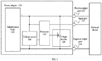
- FIG. 2 is a schematic view showing coupling of various elements of the power adapter in accordance with an embodiment of the present disclosure.
- the adapter main body 110 can include a positive output port (that is, "+” of FIG. 2 ) and a negative output port (that is, "-" of FIG. 2 ).
- the positive output port of the adapter main body 110 is coupled to the positive output port 122 of the power adapter 100, and the negative output port of the adapter main body 110 is coupled to the negative output port 124 of the power adapter 100.
- the voltage sensor 160 is arranged between the positive output port and the negative output port of the adapter main body 110, or the voltage sensor 160 is arranged between the positive output port 122 and the negative output port 124, so as to detect the output voltage of the adapter main body 110 (that is, the output voltage of the power adapter 100).
- the voltage divider 130 is arranged between the positive output port 122 and the negative output port 124. When the power adapter 100 is coupled to the external device to charge the external device, the voltage divider 130 and the external device are coupled in parallel.
- the setting of the voltage divider 130 illustrated above is just an example, and the present disclosure is not limited to this. What is needed is that the voltage divider 130 and the external device are coupled in parallel.
- the processor 140 can be arranged between the positive output port and the negative output port of the adapter main body 110, thus power can be supplied to the processor 140 via the adapter main body 110. Furthermore, the processor 140 communicates with the voltage sensor 160, thus the processor 140 can acquire data detected by the voltage sensor 160. Furthermore, the processor 140 further communicates with the input port 150, thus the processor 140 can receive indication information from the external device via the input port 150. Furthermore, the processor 140 is electrically coupled to the voltage divider 130, thus the processor 140 can transmit the control signal (for example, an electrical signal, that is, applying a voltage) to the voltage divider 130. Therefore, the processor 140 can determine whether to enable the voltage divider 130 according to the detected data or the indication information.
- the control signal for example, an electrical signal, that is, applying a voltage
- the processor 140 transits the control signal to the voltage divider 130 to cause the voltage divider 130 to work, thus the current division operation can be performed on the direct current output through the adapter main body 110, and the value of the voltage of the direct current output through the output port 120 can be reduced to be the preset value.
- the voltage output through the positive output port and the negative output port can be reduced to be less than or equal to the preset value, which can avoid damage and burst of the battery, according usage safety is improved.
- the disclosed systems, devices, and methods can be implemented by other manners.
- the device embodiments described above are only schematic.
- the units are divided according to logic functions and can be divided by another manner in an actual implementation.
- several units or assemblies can be combined or can be integrated into another system, or some features can be ignored, or are not executed.
- mutual coupling or direct coupling or communication connection shown or discussed herein can be indirect coupling or communication connection through certain interfaces, devices, or units, and can be in the form of electricity, machine, or other.
- the units illustrated as separate units can be or cannot be physically separated, and components shown in units can be or cannot be physical units, that is, can be in a place, or can be distributed in several network units. A part of or all of the units can be selected according to actual need to realize the purpose of the solution of the embodiments.
Landscapes
- Engineering & Computer Science (AREA)
- Power Engineering (AREA)
- Charge And Discharge Circuits For Batteries Or The Like (AREA)
Abstract
Description
- This application claims priority to
Chinese Patent Application No. 201510100431.X, filed on March 6, 2015 - The present disclosure relates to charging technical field, and more particularly to a power adapter.
- Presently, electronic devices (e.g., mobile phones) are generally equipped with a rechargeable battery, thus the battery can be charged by a power adapter.
- During charging, the power adapter converts an alternating current into a direct current having a specified voltage, and transmits the direct current to an electronic device. Furthermore, the electronic device includes a charging control circuit configured to control charging of the battery.
- However, when a fault occurs in the charging control circuit, a charging voltage cannot be controlled. When the charging voltage is too great, the battery may be damaged and may even burst, accordingly usage safety can be greatly affected.
- In embodiments of the present disclosure, a power adapter is provided, which can improve safety of charging.
- In a first aspect, a power adapter is provided. The power adapter comprises: an adapter main body configured to acquire an alternating current from a power source and convert the alternating current into a direct current having a specified voltage; an output port comprising a positive output port and a negative output port both electrically coupled to the adapter main body, and configured to acquire the direct current from the adapter main body, and supply the direct current to an external device via the positive output port and the negative output port; a voltage divider arranged between the positive output port and the negative output port, and configured to execute a voltage division operation upon receiving a control signal, so as to cause a value of an output voltage output through the positive output port and the negative output port to be less than or equal to a preset value; and a processor communicating with the voltage divider and configured to transmit the control signal to the voltage divider.
- In combination with the first aspect, in a first implementation manner of the first aspect, the power adapter further comprises an input port communicating with the processor, and configured to receive information from the external device and transmit the information to the processor. The processor is configured to transmit the control signal to the voltage divider upon receiving information for indicating that the output voltage needs to be reduced from the external device via the input port.
- In combination with the first aspect and the above implementation manners, in a second implementation manner of the first aspect, the power adapter further comprises a voltage sensor communicating with the processor, and configured to detect a voltage value of the direct current and transmit the voltage value to the processor. The processor is configured to transmit the control signal to the voltage divider when it is determined that the voltage value is greater than the preset value.
- In combination with the first aspect and the above implementation manners, in a third implementation manner of the first aspect, the processor is further configured to control the voltage division operation executed by the voltage divider according to the voltage value.
- In combination with the first aspect and the above implementation manners, in a fourth implementation manner of the first aspect, the voltage divider comprises a metal-oxide -semiconductor field effect transistor switch.
- In combination with the first aspect and the above implementation manners, in a fifth implementation manner of the first aspect, the voltage divider comprises a transistor switch.
- In combination with the first aspect and the above implementation manners, in a sixth implementation manner of the first aspect, the output port is configured to output the direct current to a mobile phone.
- In the embodiment of the present disclosure, by arranging the voltage divider between the positive output port and the negative output port, the voltage output through the positive output port and the negative output port can be reduced to be less than or equal to the preset value, which can avoid damage and burst of the battery, according usage safety is improved.
- To better illustrate the technical solution of embodiments of the present disclosure, the following descriptions will briefly illustrate the accompanying drawings described in the embodiments. Obviously, the following described accompanying drawings are some embodiments of the present disclosure. Those skilled in the art can obtain other accompanying drawings according to the described accompanying drawings without creative work.
-
FIG. 1 is a diagrammatic view of a power adapter in accordance with an embodiment of the present disclosure. -
FIG. 2 is a schematic circuit diagram of a power adapter in accordance with an embodiment of the present disclosure. - The technical solution of embodiments of the present disclosure will be described clearly and completely in combination with the accompanying drawings of the embodiments of the present disclosure. Obviously, the described embodiments are a part of embodiments of the present disclosure, and not all of the embodiments. According to the embodiments of the present disclosure, other embodiments obtained by those skilled in the art without creative work all fall within the protection scope of the present disclosure.
-
FIG. 1 is a diagrammatic view of apower adapter 100 in accordance with an embodiment of the present disclosure. As illustrated byFIG. 1 , thepower adapter 100 includes following. - An adapter
main body 110 is configured to acquire an alternating current from a power source, and convert the alternating current into a direct current having a specified voltage. - An
output port 120 includes a positive output port 122 and anegative output port 124 both electrically coupled to the adaptermain body 110, and is configured to acquire the direct current from the adaptermain body 110, and supply the direct current to an external device via the positive output port 122 and thenegative output port 124. - A
voltage divider 130 is arranged between the adaptermain body 110 and theoutput port 120, and is configured to execute a voltage division operation upon receiving a control signal, so as to cause a value of a voltage output through the positive output port 122 and thenegative output port 124 to be less than or equal to a preset value. - A
processor 140 communicates with thevoltage divider 130, and is configured to transmit the control signal to thevoltage divider 130. - The following will specifically illustrate various elements of the
power adapter 100. - In the embodiment of the present disclosure, the adapter
main body 110 can acquire the alternating current (or, AC voltage or AC current) from the power source, and perform an alternating-direct conversion process on the alternating current to generate the direct current having the specified voltage (for example, less than or equal to 5V). - In addition, the following will illustrate the alternating-direct conversion process.
- Firstly, a voltage transformation process is performed on the alternating current having the 220V or 110V voltage and input by the grid, so as to acquire the alternating current having the specified voltage (for example, less than or equal to 5V).
- A rectifying filter process is performed on the alternating current after the alternating current undergoes a voltage reduction process, so as to acquire the desired direct current.
- It can be understood that the above process that the adapter
main body 110 converts a high voltage alternating current into a low voltage direct current is just an example, and the present disclosure is not limited to this. - In addition, in the embodiment of the present disclosure, the structure of the adapter
main body 110 and elements of the adaptermain body 110 can be similar to that of the adapter main body of the present technology, which is not described herein to avoid repeated description. - The
output port 120 is coupled to an output port of the adaptermain body 110, and can acquire the direct current having the specified voltage from the adaptermain body 110, and transmit the direct current to the external device via electrical lines. - Furthermore, the
output port 120 can include the positive output port 122 and thenegative output port 124. - Optionally, the
output port 120 is configured to output the direct current to a mobile phone. - Specifically, in the embodiment of the present disclosure, the external device can be a mobile phone. That is, the
power adapter 100 charges a mobile phone. Accordingly, a specification and model of theoutput port 120 can be set to adapt to a corresponding charged object. For example, a universal serial bus (USB) interface (specifically, a USB interface for transmitting current) can be used as theoutput port 120. - In the embodiment of the present disclosure, the
voltage divider 130 is arranged between the positive output port 122 and thenegative output port 124. - For example, in the embodiment of the present disclosure, a port of the
voltage divider 130 can be arranged between the positive output port 122 and a positive output port of the adaptermain body 110, and the other port of thevoltage divider 130 can be arranged between thenegative output port 124 and a negative output port of the adaptermain body 110. - That is, when the
power adapter 100 is coupled to an external device to charge the external device, thevoltage divider 130 and the external device are coupled in parallel, accordingly, the voltage output to the external device can be adjusted via the voltage division operation executed by thevoltage divider 130. - Furthermore, under a normal condition, the
voltage divider 130 is in an off state, accordingly, under the normal condition, the direct current from the adaptermain body 110 can fully flow into theoutput port 120 to be output to the external device. When theprocessor 140 determines that the voltage of the direct current needs to be reduced, theprocessor 140 can transmit the control signal to thevoltage divider 130. When thevoltage divider 130 receives the control signal, thevoltage divider 130 switches to an on state, accordingly, thevoltage divider 130 can perform the current division operation on the direct current to reduce the value of the voltage of the direct current output through theoutput port 120 to be the preset value. - In addition, in the embodiment of the present disclosure, following elements can be used as the
voltage divider 130. - For example, the
voltage divider 130 includes a metal oxide semiconductor field effect transistor (MOSFET) switch. - Specifically, in the embodiment of the present disclosure, as the MOSFET has a cut-off characteristic, the MOSFET switch can be used as the
voltage divider 130. - As an example rather than limitation, when it is determined that the voltage division operation needs to be executed, a voltage (for example, 4V or 10V) can be applied to a gate of the MOSFET (for example, N-MOSFET) to turn on the MOSFET, and the positive output port 122 and the
negative output port 124 are coupled with each other when the MOSEFET is turned on. Therefore, by means of the MOSFET, the current division operation can be performed on the direct current output through the adaptermain body 110, accordingly, the voltage output through the positive output port 122 and thenegative output port 124 can be reduced. - It can be understood that the above method for using the MOSFET is just an example and not used to limit the present disclosure. Other elements which can realize the above function of the
voltage divider 130 via the MOSFET all fall within the protection scope of the present disclosure. - Optionally, the
voltage divider 130 includes a transistor switch. - Specifically, in the embodiment of the present disclosure, the above function of the
voltage divider 130 can be realized by the transistor switch. - As an example rather than limitation, when the adapter
main body 110 works normally, the output voltage of the adaptermain body 110 is less than a forward voltage for turning on the transistor switch, or the output voltage of the adaptermain body 110 is a reverse voltage for turning off the transistor switch. When it is determined that the voltage division operation needs to be executed, the forward voltage can be applied to the transistor switch to turn on the transistor switch, such that the current division operation can be performed on the direct current output through the adaptermain body 110 via the transistor switch, accordingly, the voltage output through the positive output port 122 and thenegative output port 124 can be reduced. - It can be understood that the above
illustrated voltage divider 130 is just an example and not used to limit the present disclosure. For example, thevoltage divider 130 can receive a signaling (for example, a digital signal) and recognize the signaling. When it is determined that the signaling indicates that the voltage division operation needs to be executed, the voltage division operation is executed to reduce the output voltage of thepower adapter 100. - In the embodiment of the present disclosure, the
voltage divider 130 can further include a switch (for example, a normally open relay switch) and a resistor (for example, a fixed resistor and a variable resistor). When it is determined that the voltage division operation needs to be executed, the normally open relay switch can be controlled to be turned on, so as to cause the positive output port 122 and thenegative output port 124 to be coupled with each other via the resistor, perform the current division operation on the direct current output through the adaptermain body 110 via the resistor, and reduce the voltage output through the positive output port 122 and thenegative output port 124. - In the embodiment of the present disclosure, the
processor 140 communicates with thevoltage divider 130. Furthermore, whether the output voltage of thepower adapter 100 needs to be reduced is determined. When the determination result is yes, the control signal is transmitted to thevoltage divider 130 to cause thevoltage divider 130 to work. - Furthermore, as an example rather than limitation, the following illustrates how to determine whether the output voltage of the
power adapter 100 needs to be reduced. - Optionally, the
power adapter 100 further includes aninput port 150 which communicates with theprocessor 140, and is configured to receive information from the external device, and transmit the information to theprocessor 140. - The
processor 140 is configured to transmit the control signal to thevoltage divider 130 when information for indicating that the output voltage needs to be reduced is received from the external device via theinput port 150. - Specifically, in the embodiment of the present disclosure, the
processor 140 of thepower adapter 100 can receive information from an external device (for example, a mobile phone) via theinput port 150. Therefore, for example, when the external device determines that a fault occurs in a charging control circuit of the external device, or when the external device determines that a value of the voltage provided by thepower adapter 100 is greater than a value of a secure voltage, the external device can transmit the information for indicating that the output voltage needs to be reduced to thepower adapter 100 via theinput port 150. When theprocessor 140 receives the information, theprocessor 140 transmits the control signal to thevoltage divider 130 to cause thevoltage divider 130 to work. - Furthermore, in the embodiment of the present disclosure, for example, a USB interface (specifically, a USB interface for transmitting information) can be used as the
input port 150. - Optionally, the
power adapter 100 further includes avoltage sensor 160 which communicates with theprocessor 140, and is configured to detect the voltage value of the direct current, and transmit the voltage value to theprocessor 140. - The
processor 140 transmits the control signal to thevoltage divider 130 when the voltage value is greater than a preset voltage threshold. - Specifically, in the embodiment of the present disclosure, the voltage sensor 160 (for example, a voltmeter) can be set to detect the voltage value of the direct current output through the positive output port 122 and the
negative output port 124, and transmit the voltage value to theprocessor 140. - Furthermore, a voltage threshold can be stored beforehand. Therefore, when the
processor 140 determines that the voltage value of the direct current output through the positive output port 122 and thenegative output port 124 and detected by thevoltage sensor 160 is greater than or equal to the voltage threshold, theprocessor 140 can transmit the control signal to the normally closedswitch element 130. - What needs to be illustrated is that the
voltage sensor 160 can further detect the voltage of the direct current output through the adaptermain body 110, and the present disclosure is not limited to this. - Furthermore, in the embodiment of the present disclosure, the voltage threshold can be determined according to the specification or type of the battery of the external device, for example, the voltage threshold can be 4.35V.
- It can be understood that in the embodiment of the present disclosure, the
processor 140 can be a central processing unit (CPU), and can be also a general processor, for example, a digital signal processor (DSP), an application specific integrated circuit (ASIC), a field programmable gate array (FPGA), a programmable logic device, a discrete gate or transistor logic device, a discrete hardware element, or the like. The general processor can be a micro processor, or any normal processor. - The integrated logic circuit in the form of hardware or instructions in the form of software of the
processor 140 finishes the implementation procedure. The steps of the processing method of the embodiment of the present disclosure can be finished by the hardware processor, or by the hardware and software modules of the processor. The software modules can be stored in a random access memory, a flash memory, a read-only memory, a programmable read-only memory, an electrically erasable programmable memory, a register, or a storage medium of the technical field. The storage medium is in a memory, and theprocessor 140 reads information of the memory to finish the above processing method in combination with hardware, which will not be specifically described herein to avoid repetition. -
FIG. 2 is a schematic view showing coupling of various elements of the power adapter in accordance with an embodiment of the present disclosure. As illustrated byFIG. 2 , the adaptermain body 110 can include a positive output port (that is, "+" ofFIG. 2 ) and a negative output port (that is, "-" ofFIG. 2 ). The positive output port of the adaptermain body 110 is coupled to the positive output port 122 of thepower adapter 100, and the negative output port of the adaptermain body 110 is coupled to thenegative output port 124 of thepower adapter 100. - The
voltage sensor 160 is arranged between the positive output port and the negative output port of the adaptermain body 110, or thevoltage sensor 160 is arranged between the positive output port 122 and thenegative output port 124, so as to detect the output voltage of the adapter main body 110 (that is, the output voltage of the power adapter 100). - The
voltage divider 130 is arranged between the positive output port 122 and thenegative output port 124. When thepower adapter 100 is coupled to the external device to charge the external device, thevoltage divider 130 and the external device are coupled in parallel. - What needs to be illustrated is that the setting of the
voltage divider 130 illustrated above is just an example, and the present disclosure is not limited to this. What is needed is that thevoltage divider 130 and the external device are coupled in parallel. - The
processor 140 can be arranged between the positive output port and the negative output port of the adaptermain body 110, thus power can be supplied to theprocessor 140 via the adaptermain body 110. Furthermore, theprocessor 140 communicates with thevoltage sensor 160, thus theprocessor 140 can acquire data detected by thevoltage sensor 160. Furthermore, theprocessor 140 further communicates with theinput port 150, thus theprocessor 140 can receive indication information from the external device via theinput port 150. Furthermore, theprocessor 140 is electrically coupled to thevoltage divider 130, thus theprocessor 140 can transmit the control signal (for example, an electrical signal, that is, applying a voltage) to thevoltage divider 130. Therefore, theprocessor 140 can determine whether to enable thevoltage divider 130 according to the detected data or the indication information. When the determination result is yes, theprocessor 140 transits the control signal to thevoltage divider 130 to cause thevoltage divider 130 to work, thus the current division operation can be performed on the direct current output through the adaptermain body 110, and the value of the voltage of the direct current output through theoutput port 120 can be reduced to be the preset value. - In the embodiment of the present disclosure, by arranging the voltage divider between the positive output port and the negative output port, the voltage output through the positive output port and the negative output port can be reduced to be less than or equal to the preset value, which can avoid damage and burst of the battery, according usage safety is improved.
- Those skilled in the art can appreciate that units and steps of various examples described in the embodiments of the present disclosure can be realized by electronic hardware or a combination of computer software and electronic hardware. Whether these functions are realized by hardware or software depends on particular applications and design constraint conditions. For each particular application, professionals can employ different methods to realize described functions, but this realization should fall into the scope of the present disclosure.
- In several embodiments provided by the present disclosure, it can be understood that the disclosed systems, devices, and methods can be implemented by other manners. For example, the device embodiments described above are only schematic. For example, the units are divided according to logic functions and can be divided by another manner in an actual implementation. For example, several units or assemblies can be combined or can be integrated into another system, or some features can be ignored, or are not executed. Another point is that mutual coupling or direct coupling or communication connection shown or discussed herein can be indirect coupling or communication connection through certain interfaces, devices, or units, and can be in the form of electricity, machine, or other.
- The units illustrated as separate units can be or cannot be physically separated, and components shown in units can be or cannot be physical units, that is, can be in a place, or can be distributed in several network units. A part of or all of the units can be selected according to actual need to realize the purpose of the solution of the embodiments.
- The foregoing descriptions are merely preferred embodiments of the present disclosure, rather than limiting the present disclosure. Any one skilled in the art can easily make change or alterations within the technology range of the present disclosure, and those change or alterations shall fall within the protection scope of the present disclosure. Therefore, the protection scope of the present disclosure shall be limited by the protection scope of the claims.
Claims (7)
- A power adapter comprising:an adapter main body configured to acquire an alternating current from a power source and convert the alternating current into a direct current having a specified voltage ;an output port comprising a positive output port and a negative output port both electrically coupled to the adapter main body, and configured to acquire the direct current from the adapter main body, and supply the direct current to an external device via the positive output port and the negative output port;a voltage divider arranged between the positive output port and the negative output port, and configured to execute a voltage division operation upon receiving a control signal, so as to cause a value of an output voltage output through the positive output port and the negative output port to be less than or equal to a preset value; anda processor communicating with the voltage divider and configured to transmit the control signal to the voltage divider.
- The power adapter of claim 1, wherein the power adapter further comprises:an input port communicating with the processor, and configured to receive information from the external device and transmit the information to the processor; andthe processor is configured to transmit the control signal to the voltage divider upon receiving information for indicating that the output voltage needs to be reduced from the external device via the input port.
- The power adapter of claim 1 or claim 2, wherein the power adapter further comprises:a voltage sensor communicating with the processor, and configured to detect a voltage value of the direct current and transmit the voltage value to the processor; andthe processor is configured to transmit the control signal to the voltage divider when it is determined that the voltage value is greater than the preset value.
- The power adapter of claim 3, wherein the processor is further configured to control the voltage division operation executed by the voltage divider according to the voltage value.
- The power adapter of claim 1 or claim 2, wherein the voltage divider comprises a metal-oxide -semiconductor field effect transistor switch.
- The power adapter of claim 1 or claim 2, wherein the voltage divider comprises a transistor switch.
- The power adapter of claim 1 or claim 2, wherein the output port is configured to output the direct current to a mobile phone.
Applications Claiming Priority (2)
| Application Number | Priority Date | Filing Date | Title |
|---|---|---|---|
| CN201510100431.XA CN104753367B (en) | 2015-03-06 | 2015-03-06 | Power adapter |
| PCT/CN2016/074907 WO2016141814A1 (en) | 2015-03-06 | 2016-02-29 | Power adapter |
Publications (2)
| Publication Number | Publication Date |
|---|---|
| EP3160005A1 true EP3160005A1 (en) | 2017-04-26 |
| EP3160005A4 EP3160005A4 (en) | 2018-06-20 |
Family
ID=53592594
Family Applications (1)
| Application Number | Title | Priority Date | Filing Date |
|---|---|---|---|
| EP16761041.9A Ceased EP3160005A4 (en) | 2015-03-06 | 2016-02-29 | Power adapter |
Country Status (4)
| Country | Link |
|---|---|
| US (1) | US10003213B2 (en) |
| EP (1) | EP3160005A4 (en) |
| CN (1) | CN104753367B (en) |
| WO (1) | WO2016141814A1 (en) |
Families Citing this family (2)
| Publication number | Priority date | Publication date | Assignee | Title |
|---|---|---|---|---|
| CN104753367B (en) * | 2015-03-06 | 2016-10-19 | 广东欧珀移动通信有限公司 | Power adapter |
| US9870014B1 (en) * | 2017-02-03 | 2018-01-16 | SK Hynix Inc. | Digital low drop-out regulator |
Family Cites Families (18)
| Publication number | Priority date | Publication date | Assignee | Title |
|---|---|---|---|---|
| US6023419A (en) * | 1997-12-08 | 2000-02-08 | Yang; Tai-Her | Capacitor regulated controllable voltage and current power supply |
| DE20021056U1 (en) * | 2000-12-12 | 2001-06-28 | Yang, Tai Her, Si-Hu, Dzan Hwa | Output circuit automatically controlled by a secondary circuit with a stored voltage or an opposite electromotive force as a load |
| US7836322B2 (en) * | 2002-12-21 | 2010-11-16 | Power-One, Inc. | System for controlling an array of point-of-load regulators and auxiliary devices |
| JP4066901B2 (en) * | 2003-07-03 | 2008-03-26 | ソニー株式会社 | Power adapter and power supply system |
| JP4692554B2 (en) * | 2008-02-06 | 2011-06-01 | ソニー株式会社 | Charger |
| US7826190B2 (en) * | 2008-03-19 | 2010-11-02 | Universal Scientific Industrial Co., Ltd. | Over-voltage protection device |
| US8674544B2 (en) * | 2009-01-26 | 2014-03-18 | Geneva Cleantech, Inc. | Methods and apparatus for power factor correction and reduction of distortion in and noise in a power supply delivery network |
| JP2011172426A (en) * | 2010-02-22 | 2011-09-01 | Nippon Seiki Co Ltd | Power supply apparatus |
| EP2369725B1 (en) * | 2010-03-25 | 2012-09-26 | ABB Schweiz AG | Short circuiting unit |
| US20130015714A1 (en) * | 2011-07-15 | 2013-01-17 | Kwok Leo Y | Smart Power Portal |
| EP2608344A1 (en) * | 2011-12-19 | 2013-06-26 | Siemens Aktiengesellschaft | Method for protecting an intermediate circuit condenser in a frequency converter circuit |
| US20140062191A1 (en) * | 2012-08-29 | 2014-03-06 | Robert L. Bryson | Low Voltage Solar Electric Energy Distribution |
| CN104113039A (en) * | 2013-04-19 | 2014-10-22 | 鸿富锦精密电子(天津)有限公司 | Over-voltage protection circuit |
| CN103701182A (en) * | 2013-12-16 | 2014-04-02 | 小米科技有限责任公司 | Charger, electronic equipment and charging system |
| CN103762691B (en) * | 2014-01-28 | 2015-12-23 | 广东欧珀移动通信有限公司 | Battery charger and cell charge protection control method |
| CN103795040B (en) * | 2014-01-28 | 2016-11-09 | 广东欧珀移动通信有限公司 | Electronic equipment and its power adapter |
| CN104753367B (en) * | 2015-03-06 | 2016-10-19 | 广东欧珀移动通信有限公司 | Power adapter |
| CN204559413U (en) * | 2015-03-06 | 2015-08-12 | 广东欧珀移动通信有限公司 | Power Adapter |
-
2015
- 2015-03-06 CN CN201510100431.XA patent/CN104753367B/en active Active
-
2016
- 2016-02-29 WO PCT/CN2016/074907 patent/WO2016141814A1/en not_active Ceased
- 2016-02-29 EP EP16761041.9A patent/EP3160005A4/en not_active Ceased
-
2017
- 2017-01-11 US US15/403,680 patent/US10003213B2/en active Active
Also Published As
| Publication number | Publication date |
|---|---|
| CN104753367A (en) | 2015-07-01 |
| WO2016141814A1 (en) | 2016-09-15 |
| EP3160005A4 (en) | 2018-06-20 |
| US10003213B2 (en) | 2018-06-19 |
| CN104753367B (en) | 2016-10-19 |
| US20170126050A1 (en) | 2017-05-04 |
Similar Documents
| Publication | Publication Date | Title |
|---|---|---|
| EP3098931B1 (en) | Charging circuit and terminal | |
| US12487290B2 (en) | Charging/discharging protection circuit, terminal device, and battery discharging control method | |
| EP3543827A1 (en) | Electronic device, charger, charging system and charging method | |
| CN104852439B (en) | Electronic equipment and double-battery charge electric discharge switching method | |
| US11041889B2 (en) | Method for estimating load current of power supply, and USB-type converter | |
| EP2854253B1 (en) | Charger, charging terminal, charging system and control method for charging | |
| EP2991156B1 (en) | Method and device for performing large-current charging on intelligent terminal | |
| EP3197008A1 (en) | Charging device for mobile terminal | |
| EP3086433A1 (en) | Charging method, alternating current adaptor, charging management device and terminal | |
| CN108318741A (en) | A kind of impedance detection circuit and detection method | |
| PH12016501485A1 (en) | Electronic device and power adapter | |
| CN203422413U (en) | A conductive charging pilot signal detection circuit and system for electric vehicles | |
| EP3700045A1 (en) | Charging device and charging system | |
| CN207117578U (en) | Protection circuit | |
| CN104215810B (en) | Electric automobile conduction type charging guide signal detection circuit and system | |
| US10003213B2 (en) | Power adapter | |
| CN106797414A (en) | A terminal leakage current detection circuit and terminal | |
| CN107612052A (en) | The charging method and mobile terminal of mobile terminal | |
| CN204425017U (en) | Power supply adaptor | |
| CN204559413U (en) | Power Adapter | |
| CN207475279U (en) | Energy-efficient emergency power supply control switching circuit | |
| CN104752783A (en) | Terminal battery activation method, device and terminal | |
| CN205304279U (en) | Charge protection and identification circuit and rechargeable devices | |
| CN104682522A (en) | Charger for battery | |
| CN110266076B (en) | Charging control system for walking robot |
Legal Events
| Date | Code | Title | Description |
|---|---|---|---|
| STAA | Information on the status of an ep patent application or granted ep patent |
Free format text: STATUS: THE INTERNATIONAL PUBLICATION HAS BEEN MADE |
|
| PUAI | Public reference made under article 153(3) epc to a published international application that has entered the european phase |
Free format text: ORIGINAL CODE: 0009012 |
|
| STAA | Information on the status of an ep patent application or granted ep patent |
Free format text: STATUS: REQUEST FOR EXAMINATION WAS MADE |
|
| 17P | Request for examination filed |
Effective date: 20170120 |
|
| AK | Designated contracting states |
Kind code of ref document: A1 Designated state(s): AL AT BE BG CH CY CZ DE DK EE ES FI FR GB GR HR HU IE IS IT LI LT LU LV MC MK MT NL NO PL PT RO RS SE SI SK SM TR |
|
| AX | Request for extension of the european patent |
Extension state: BA ME |
|
| DAV | Request for validation of the european patent (deleted) | ||
| DAX | Request for extension of the european patent (deleted) | ||
| A4 | Supplementary search report drawn up and despatched |
Effective date: 20180523 |
|
| RIC1 | Information provided on ipc code assigned before grant |
Ipc: H02J 7/04 20060101AFI20180516BHEP Ipc: H02M 7/04 20060101ALI20180516BHEP |
|
| STAA | Information on the status of an ep patent application or granted ep patent |
Free format text: STATUS: EXAMINATION IS IN PROGRESS |
|
| 17Q | First examination report despatched |
Effective date: 20190521 |
|
| RAP1 | Party data changed (applicant data changed or rights of an application transferred) |
Owner name: GUANGDONG OPPO MOBILE TELECOMMUNICATIONS CORP., LT |
|
| REG | Reference to a national code |
Ref country code: DE Ref legal event code: R003 |
|
| STAA | Information on the status of an ep patent application or granted ep patent |
Free format text: STATUS: THE APPLICATION HAS BEEN REFUSED |
|
| 18R | Application refused |
Effective date: 20211022 |