EP3159428A1 - Multilayer film and method for manufacturing same - Google Patents
Multilayer film and method for manufacturing same Download PDFInfo
- Publication number
- EP3159428A1 EP3159428A1 EP15809725.3A EP15809725A EP3159428A1 EP 3159428 A1 EP3159428 A1 EP 3159428A1 EP 15809725 A EP15809725 A EP 15809725A EP 3159428 A1 EP3159428 A1 EP 3159428A1
- Authority
- EP
- European Patent Office
- Prior art keywords
- film
- substrate
- dielectric layer
- layer
- seed layer
- Prior art date
- Legal status (The legal status is an assumption and is not a legal conclusion. Google has not performed a legal analysis and makes no representation as to the accuracy of the status listed.)
- Withdrawn
Links
- 238000004519 manufacturing process Methods 0.000 title claims abstract description 25
- 238000000034 method Methods 0.000 title description 11
- 239000000758 substrate Substances 0.000 claims abstract description 84
- 238000004544 sputter deposition Methods 0.000 claims abstract description 43
- 150000001875 compounds Chemical class 0.000 claims abstract description 27
- 229910052760 oxygen Inorganic materials 0.000 claims abstract description 18
- QVGXLLKOCUKJST-UHFFFAOYSA-N atomic oxygen Chemical compound [O] QVGXLLKOCUKJST-UHFFFAOYSA-N 0.000 claims abstract description 17
- 239000001301 oxygen Substances 0.000 claims abstract description 17
- 229910052707 ruthenium Inorganic materials 0.000 claims abstract description 13
- 229910052712 strontium Inorganic materials 0.000 claims abstract description 13
- KJTLSVCANCCWHF-UHFFFAOYSA-N Ruthenium Chemical compound [Ru] KJTLSVCANCCWHF-UHFFFAOYSA-N 0.000 claims abstract description 12
- CIOAGBVUUVVLOB-UHFFFAOYSA-N strontium atom Chemical compound [Sr] CIOAGBVUUVVLOB-UHFFFAOYSA-N 0.000 claims abstract description 12
- -1 strontium (Sr) Chemical class 0.000 claims abstract description 10
- BASFCYQUMIYNBI-UHFFFAOYSA-N platinum Chemical compound [Pt] BASFCYQUMIYNBI-UHFFFAOYSA-N 0.000 claims description 24
- 238000002441 X-ray diffraction Methods 0.000 claims description 14
- 239000010936 titanium Substances 0.000 claims description 11
- MCMNRKCIXSYSNV-UHFFFAOYSA-N Zirconium dioxide Chemical compound O=[Zr]=O MCMNRKCIXSYSNV-UHFFFAOYSA-N 0.000 claims description 10
- 229910052710 silicon Inorganic materials 0.000 claims description 8
- 239000010703 silicon Substances 0.000 claims description 8
- RTAQQCXQSZGOHL-UHFFFAOYSA-N Titanium Chemical compound [Ti] RTAQQCXQSZGOHL-UHFFFAOYSA-N 0.000 claims description 5
- 229910052719 titanium Inorganic materials 0.000 claims description 5
- 229910020279 Pb(Zr, Ti)O3 Inorganic materials 0.000 claims description 4
- 229910052697 platinum Inorganic materials 0.000 claims description 4
- 239000010408 film Substances 0.000 description 139
- 229910052451 lead zirconate titanate Inorganic materials 0.000 description 48
- 230000015572 biosynthetic process Effects 0.000 description 26
- 229910002353 SrRuO3 Inorganic materials 0.000 description 20
- 239000007789 gas Substances 0.000 description 17
- 230000020169 heat generation Effects 0.000 description 11
- 238000010438 heat treatment Methods 0.000 description 8
- XUIMIQQOPSSXEZ-UHFFFAOYSA-N Silicon Chemical compound [Si] XUIMIQQOPSSXEZ-UHFFFAOYSA-N 0.000 description 7
- 239000013078 crystal Substances 0.000 description 7
- 238000001816 cooling Methods 0.000 description 5
- 238000000151 deposition Methods 0.000 description 5
- 230000008021 deposition Effects 0.000 description 5
- 238000012546 transfer Methods 0.000 description 5
- VYPSYNLAJGMNEJ-UHFFFAOYSA-N silicon dioxide Inorganic materials O=[Si]=O VYPSYNLAJGMNEJ-UHFFFAOYSA-N 0.000 description 4
- 239000010409 thin film Substances 0.000 description 4
- 229910020289 Pb(ZrxTi1-x)O3 Inorganic materials 0.000 description 3
- 229910020273 Pb(ZrxTi1−x)O3 Inorganic materials 0.000 description 3
- 238000010586 diagram Methods 0.000 description 3
- HFGPZNIAWCZYJU-UHFFFAOYSA-N lead zirconate titanate Chemical compound [O-2].[O-2].[O-2].[O-2].[O-2].[Ti+4].[Zr+4].[Pb+2] HFGPZNIAWCZYJU-UHFFFAOYSA-N 0.000 description 3
- 239000000463 material Substances 0.000 description 3
- 239000002245 particle Substances 0.000 description 3
- MYMOFIZGZYHOMD-UHFFFAOYSA-N Dioxygen Chemical compound O=O MYMOFIZGZYHOMD-UHFFFAOYSA-N 0.000 description 2
- PNEYBMLMFCGWSK-UHFFFAOYSA-N aluminium oxide Inorganic materials [O-2].[O-2].[O-2].[Al+3].[Al+3] PNEYBMLMFCGWSK-UHFFFAOYSA-N 0.000 description 2
- 239000000919 ceramic Substances 0.000 description 2
- 239000002826 coolant Substances 0.000 description 2
- 229910001882 dioxygen Inorganic materials 0.000 description 2
- 230000000694 effects Effects 0.000 description 2
- 230000001590 oxidative effect Effects 0.000 description 2
- 239000010453 quartz Substances 0.000 description 2
- 229910003781 PbTiO3 Inorganic materials 0.000 description 1
- 230000001133 acceleration Effects 0.000 description 1
- 238000000137 annealing Methods 0.000 description 1
- 229910002113 barium titanate Inorganic materials 0.000 description 1
- 229910052681 coesite Inorganic materials 0.000 description 1
- 230000006835 compression Effects 0.000 description 1
- 238000007906 compression Methods 0.000 description 1
- 229910052906 cristobalite Inorganic materials 0.000 description 1
- 238000002425 crystallisation Methods 0.000 description 1
- 230000008025 crystallization Effects 0.000 description 1
- 238000011161 development Methods 0.000 description 1
- 238000011156 evaluation Methods 0.000 description 1
- 238000002474 experimental method Methods 0.000 description 1
- 238000002955 isolation Methods 0.000 description 1
- 238000001755 magnetron sputter deposition Methods 0.000 description 1
- 238000005259 measurement Methods 0.000 description 1
- 238000012986 modification Methods 0.000 description 1
- 230000004048 modification Effects 0.000 description 1
- 230000003647 oxidation Effects 0.000 description 1
- 238000007254 oxidation reaction Methods 0.000 description 1
- 238000000634 powder X-ray diffraction Methods 0.000 description 1
- 238000005086 pumping Methods 0.000 description 1
- 238000011160 research Methods 0.000 description 1
- 239000000377 silicon dioxide Substances 0.000 description 1
- 229910052682 stishovite Inorganic materials 0.000 description 1
- 229910052905 tridymite Inorganic materials 0.000 description 1
Images




Classifications
-
- C—CHEMISTRY; METALLURGY
- C23—COATING METALLIC MATERIAL; COATING MATERIAL WITH METALLIC MATERIAL; CHEMICAL SURFACE TREATMENT; DIFFUSION TREATMENT OF METALLIC MATERIAL; COATING BY VACUUM EVAPORATION, BY SPUTTERING, BY ION IMPLANTATION OR BY CHEMICAL VAPOUR DEPOSITION, IN GENERAL; INHIBITING CORROSION OF METALLIC MATERIAL OR INCRUSTATION IN GENERAL
- C23C—COATING METALLIC MATERIAL; COATING MATERIAL WITH METALLIC MATERIAL; SURFACE TREATMENT OF METALLIC MATERIAL BY DIFFUSION INTO THE SURFACE, BY CHEMICAL CONVERSION OR SUBSTITUTION; COATING BY VACUUM EVAPORATION, BY SPUTTERING, BY ION IMPLANTATION OR BY CHEMICAL VAPOUR DEPOSITION, IN GENERAL
- C23C14/00—Coating by vacuum evaporation, by sputtering or by ion implantation of the coating forming material
- C23C14/22—Coating by vacuum evaporation, by sputtering or by ion implantation of the coating forming material characterised by the process of coating
- C23C14/54—Controlling or regulating the coating process
- C23C14/541—Heating or cooling of the substrates
-
- C—CHEMISTRY; METALLURGY
- C01—INORGANIC CHEMISTRY
- C01G—COMPOUNDS CONTAINING METALS NOT COVERED BY SUBCLASSES C01D OR C01F
- C01G25/00—Compounds of zirconium
-
- C—CHEMISTRY; METALLURGY
- C01—INORGANIC CHEMISTRY
- C01G—COMPOUNDS CONTAINING METALS NOT COVERED BY SUBCLASSES C01D OR C01F
- C01G25/00—Compounds of zirconium
- C01G25/006—Compounds containing zirconium, with or without oxygen or hydrogen, and containing two or more other elements
-
- C—CHEMISTRY; METALLURGY
- C01—INORGANIC CHEMISTRY
- C01G—COMPOUNDS CONTAINING METALS NOT COVERED BY SUBCLASSES C01D OR C01F
- C01G55/00—Compounds of ruthenium, rhodium, palladium, osmium, iridium, or platinum
-
- C—CHEMISTRY; METALLURGY
- C01—INORGANIC CHEMISTRY
- C01G—COMPOUNDS CONTAINING METALS NOT COVERED BY SUBCLASSES C01D OR C01F
- C01G55/00—Compounds of ruthenium, rhodium, palladium, osmium, iridium, or platinum
- C01G55/002—Compounds containing ruthenium, rhodium, palladium, osmium, iridium or platinum, with or without oxygen or hydrogen, and containing two or more other elements
-
- C—CHEMISTRY; METALLURGY
- C23—COATING METALLIC MATERIAL; COATING MATERIAL WITH METALLIC MATERIAL; CHEMICAL SURFACE TREATMENT; DIFFUSION TREATMENT OF METALLIC MATERIAL; COATING BY VACUUM EVAPORATION, BY SPUTTERING, BY ION IMPLANTATION OR BY CHEMICAL VAPOUR DEPOSITION, IN GENERAL; INHIBITING CORROSION OF METALLIC MATERIAL OR INCRUSTATION IN GENERAL
- C23C—COATING METALLIC MATERIAL; COATING MATERIAL WITH METALLIC MATERIAL; SURFACE TREATMENT OF METALLIC MATERIAL BY DIFFUSION INTO THE SURFACE, BY CHEMICAL CONVERSION OR SUBSTITUTION; COATING BY VACUUM EVAPORATION, BY SPUTTERING, BY ION IMPLANTATION OR BY CHEMICAL VAPOUR DEPOSITION, IN GENERAL
- C23C14/00—Coating by vacuum evaporation, by sputtering or by ion implantation of the coating forming material
- C23C14/02—Pretreatment of the material to be coated
- C23C14/024—Deposition of sublayers, e.g. to promote adhesion of the coating
-
- C—CHEMISTRY; METALLURGY
- C23—COATING METALLIC MATERIAL; COATING MATERIAL WITH METALLIC MATERIAL; CHEMICAL SURFACE TREATMENT; DIFFUSION TREATMENT OF METALLIC MATERIAL; COATING BY VACUUM EVAPORATION, BY SPUTTERING, BY ION IMPLANTATION OR BY CHEMICAL VAPOUR DEPOSITION, IN GENERAL; INHIBITING CORROSION OF METALLIC MATERIAL OR INCRUSTATION IN GENERAL
- C23C—COATING METALLIC MATERIAL; COATING MATERIAL WITH METALLIC MATERIAL; SURFACE TREATMENT OF METALLIC MATERIAL BY DIFFUSION INTO THE SURFACE, BY CHEMICAL CONVERSION OR SUBSTITUTION; COATING BY VACUUM EVAPORATION, BY SPUTTERING, BY ION IMPLANTATION OR BY CHEMICAL VAPOUR DEPOSITION, IN GENERAL
- C23C14/00—Coating by vacuum evaporation, by sputtering or by ion implantation of the coating forming material
- C23C14/06—Coating by vacuum evaporation, by sputtering or by ion implantation of the coating forming material characterised by the coating material
-
- C—CHEMISTRY; METALLURGY
- C23—COATING METALLIC MATERIAL; COATING MATERIAL WITH METALLIC MATERIAL; CHEMICAL SURFACE TREATMENT; DIFFUSION TREATMENT OF METALLIC MATERIAL; COATING BY VACUUM EVAPORATION, BY SPUTTERING, BY ION IMPLANTATION OR BY CHEMICAL VAPOUR DEPOSITION, IN GENERAL; INHIBITING CORROSION OF METALLIC MATERIAL OR INCRUSTATION IN GENERAL
- C23C—COATING METALLIC MATERIAL; COATING MATERIAL WITH METALLIC MATERIAL; SURFACE TREATMENT OF METALLIC MATERIAL BY DIFFUSION INTO THE SURFACE, BY CHEMICAL CONVERSION OR SUBSTITUTION; COATING BY VACUUM EVAPORATION, BY SPUTTERING, BY ION IMPLANTATION OR BY CHEMICAL VAPOUR DEPOSITION, IN GENERAL
- C23C14/00—Coating by vacuum evaporation, by sputtering or by ion implantation of the coating forming material
- C23C14/06—Coating by vacuum evaporation, by sputtering or by ion implantation of the coating forming material characterised by the coating material
- C23C14/08—Oxides
-
- C—CHEMISTRY; METALLURGY
- C23—COATING METALLIC MATERIAL; COATING MATERIAL WITH METALLIC MATERIAL; CHEMICAL SURFACE TREATMENT; DIFFUSION TREATMENT OF METALLIC MATERIAL; COATING BY VACUUM EVAPORATION, BY SPUTTERING, BY ION IMPLANTATION OR BY CHEMICAL VAPOUR DEPOSITION, IN GENERAL; INHIBITING CORROSION OF METALLIC MATERIAL OR INCRUSTATION IN GENERAL
- C23C—COATING METALLIC MATERIAL; COATING MATERIAL WITH METALLIC MATERIAL; SURFACE TREATMENT OF METALLIC MATERIAL BY DIFFUSION INTO THE SURFACE, BY CHEMICAL CONVERSION OR SUBSTITUTION; COATING BY VACUUM EVAPORATION, BY SPUTTERING, BY ION IMPLANTATION OR BY CHEMICAL VAPOUR DEPOSITION, IN GENERAL
- C23C14/00—Coating by vacuum evaporation, by sputtering or by ion implantation of the coating forming material
- C23C14/06—Coating by vacuum evaporation, by sputtering or by ion implantation of the coating forming material characterised by the coating material
- C23C14/08—Oxides
- C23C14/088—Oxides of the type ABO3 with A representing alkali, alkaline earth metal or Pb and B representing a refractory or rare earth metal
-
- C—CHEMISTRY; METALLURGY
- C23—COATING METALLIC MATERIAL; COATING MATERIAL WITH METALLIC MATERIAL; CHEMICAL SURFACE TREATMENT; DIFFUSION TREATMENT OF METALLIC MATERIAL; COATING BY VACUUM EVAPORATION, BY SPUTTERING, BY ION IMPLANTATION OR BY CHEMICAL VAPOUR DEPOSITION, IN GENERAL; INHIBITING CORROSION OF METALLIC MATERIAL OR INCRUSTATION IN GENERAL
- C23C—COATING METALLIC MATERIAL; COATING MATERIAL WITH METALLIC MATERIAL; SURFACE TREATMENT OF METALLIC MATERIAL BY DIFFUSION INTO THE SURFACE, BY CHEMICAL CONVERSION OR SUBSTITUTION; COATING BY VACUUM EVAPORATION, BY SPUTTERING, BY ION IMPLANTATION OR BY CHEMICAL VAPOUR DEPOSITION, IN GENERAL
- C23C14/00—Coating by vacuum evaporation, by sputtering or by ion implantation of the coating forming material
- C23C14/06—Coating by vacuum evaporation, by sputtering or by ion implantation of the coating forming material characterised by the coating material
- C23C14/14—Metallic material, boron or silicon
- C23C14/16—Metallic material, boron or silicon on metallic substrates or on substrates of boron or silicon
- C23C14/165—Metallic material, boron or silicon on metallic substrates or on substrates of boron or silicon by cathodic sputtering
-
- C—CHEMISTRY; METALLURGY
- C23—COATING METALLIC MATERIAL; COATING MATERIAL WITH METALLIC MATERIAL; CHEMICAL SURFACE TREATMENT; DIFFUSION TREATMENT OF METALLIC MATERIAL; COATING BY VACUUM EVAPORATION, BY SPUTTERING, BY ION IMPLANTATION OR BY CHEMICAL VAPOUR DEPOSITION, IN GENERAL; INHIBITING CORROSION OF METALLIC MATERIAL OR INCRUSTATION IN GENERAL
- C23C—COATING METALLIC MATERIAL; COATING MATERIAL WITH METALLIC MATERIAL; SURFACE TREATMENT OF METALLIC MATERIAL BY DIFFUSION INTO THE SURFACE, BY CHEMICAL CONVERSION OR SUBSTITUTION; COATING BY VACUUM EVAPORATION, BY SPUTTERING, BY ION IMPLANTATION OR BY CHEMICAL VAPOUR DEPOSITION, IN GENERAL
- C23C14/00—Coating by vacuum evaporation, by sputtering or by ion implantation of the coating forming material
- C23C14/22—Coating by vacuum evaporation, by sputtering or by ion implantation of the coating forming material characterised by the process of coating
- C23C14/34—Sputtering
-
- C—CHEMISTRY; METALLURGY
- C23—COATING METALLIC MATERIAL; COATING MATERIAL WITH METALLIC MATERIAL; CHEMICAL SURFACE TREATMENT; DIFFUSION TREATMENT OF METALLIC MATERIAL; COATING BY VACUUM EVAPORATION, BY SPUTTERING, BY ION IMPLANTATION OR BY CHEMICAL VAPOUR DEPOSITION, IN GENERAL; INHIBITING CORROSION OF METALLIC MATERIAL OR INCRUSTATION IN GENERAL
- C23C—COATING METALLIC MATERIAL; COATING MATERIAL WITH METALLIC MATERIAL; SURFACE TREATMENT OF METALLIC MATERIAL BY DIFFUSION INTO THE SURFACE, BY CHEMICAL CONVERSION OR SUBSTITUTION; COATING BY VACUUM EVAPORATION, BY SPUTTERING, BY ION IMPLANTATION OR BY CHEMICAL VAPOUR DEPOSITION, IN GENERAL
- C23C14/00—Coating by vacuum evaporation, by sputtering or by ion implantation of the coating forming material
- C23C14/22—Coating by vacuum evaporation, by sputtering or by ion implantation of the coating forming material characterised by the process of coating
- C23C14/34—Sputtering
- C23C14/35—Sputtering by application of a magnetic field, e.g. magnetron sputtering
-
- C—CHEMISTRY; METALLURGY
- C23—COATING METALLIC MATERIAL; COATING MATERIAL WITH METALLIC MATERIAL; CHEMICAL SURFACE TREATMENT; DIFFUSION TREATMENT OF METALLIC MATERIAL; COATING BY VACUUM EVAPORATION, BY SPUTTERING, BY ION IMPLANTATION OR BY CHEMICAL VAPOUR DEPOSITION, IN GENERAL; INHIBITING CORROSION OF METALLIC MATERIAL OR INCRUSTATION IN GENERAL
- C23C—COATING METALLIC MATERIAL; COATING MATERIAL WITH METALLIC MATERIAL; SURFACE TREATMENT OF METALLIC MATERIAL BY DIFFUSION INTO THE SURFACE, BY CHEMICAL CONVERSION OR SUBSTITUTION; COATING BY VACUUM EVAPORATION, BY SPUTTERING, BY ION IMPLANTATION OR BY CHEMICAL VAPOUR DEPOSITION, IN GENERAL
- C23C14/00—Coating by vacuum evaporation, by sputtering or by ion implantation of the coating forming material
- C23C14/22—Coating by vacuum evaporation, by sputtering or by ion implantation of the coating forming material characterised by the process of coating
- C23C14/56—Apparatus specially adapted for continuous coating; Arrangements for maintaining the vacuum, e.g. vacuum locks
- C23C14/568—Transferring the substrates through a series of coating stations
-
- C—CHEMISTRY; METALLURGY
- C23—COATING METALLIC MATERIAL; COATING MATERIAL WITH METALLIC MATERIAL; CHEMICAL SURFACE TREATMENT; DIFFUSION TREATMENT OF METALLIC MATERIAL; COATING BY VACUUM EVAPORATION, BY SPUTTERING, BY ION IMPLANTATION OR BY CHEMICAL VAPOUR DEPOSITION, IN GENERAL; INHIBITING CORROSION OF METALLIC MATERIAL OR INCRUSTATION IN GENERAL
- C23C—COATING METALLIC MATERIAL; COATING MATERIAL WITH METALLIC MATERIAL; SURFACE TREATMENT OF METALLIC MATERIAL BY DIFFUSION INTO THE SURFACE, BY CHEMICAL CONVERSION OR SUBSTITUTION; COATING BY VACUUM EVAPORATION, BY SPUTTERING, BY ION IMPLANTATION OR BY CHEMICAL VAPOUR DEPOSITION, IN GENERAL
- C23C28/00—Coating for obtaining at least two superposed coatings either by methods not provided for in a single one of groups C23C2/00 - C23C26/00 or by combinations of methods provided for in subclasses C23C and C25C or C25D
- C23C28/30—Coatings combining at least one metallic layer and at least one inorganic non-metallic layer
-
- C—CHEMISTRY; METALLURGY
- C23—COATING METALLIC MATERIAL; COATING MATERIAL WITH METALLIC MATERIAL; CHEMICAL SURFACE TREATMENT; DIFFUSION TREATMENT OF METALLIC MATERIAL; COATING BY VACUUM EVAPORATION, BY SPUTTERING, BY ION IMPLANTATION OR BY CHEMICAL VAPOUR DEPOSITION, IN GENERAL; INHIBITING CORROSION OF METALLIC MATERIAL OR INCRUSTATION IN GENERAL
- C23C—COATING METALLIC MATERIAL; COATING MATERIAL WITH METALLIC MATERIAL; SURFACE TREATMENT OF METALLIC MATERIAL BY DIFFUSION INTO THE SURFACE, BY CHEMICAL CONVERSION OR SUBSTITUTION; COATING BY VACUUM EVAPORATION, BY SPUTTERING, BY ION IMPLANTATION OR BY CHEMICAL VAPOUR DEPOSITION, IN GENERAL
- C23C28/00—Coating for obtaining at least two superposed coatings either by methods not provided for in a single one of groups C23C2/00 - C23C26/00 or by combinations of methods provided for in subclasses C23C and C25C or C25D
- C23C28/30—Coatings combining at least one metallic layer and at least one inorganic non-metallic layer
- C23C28/32—Coatings combining at least one metallic layer and at least one inorganic non-metallic layer including at least one pure metallic layer
-
- C—CHEMISTRY; METALLURGY
- C23—COATING METALLIC MATERIAL; COATING MATERIAL WITH METALLIC MATERIAL; CHEMICAL SURFACE TREATMENT; DIFFUSION TREATMENT OF METALLIC MATERIAL; COATING BY VACUUM EVAPORATION, BY SPUTTERING, BY ION IMPLANTATION OR BY CHEMICAL VAPOUR DEPOSITION, IN GENERAL; INHIBITING CORROSION OF METALLIC MATERIAL OR INCRUSTATION IN GENERAL
- C23C—COATING METALLIC MATERIAL; COATING MATERIAL WITH METALLIC MATERIAL; SURFACE TREATMENT OF METALLIC MATERIAL BY DIFFUSION INTO THE SURFACE, BY CHEMICAL CONVERSION OR SUBSTITUTION; COATING BY VACUUM EVAPORATION, BY SPUTTERING, BY ION IMPLANTATION OR BY CHEMICAL VAPOUR DEPOSITION, IN GENERAL
- C23C28/00—Coating for obtaining at least two superposed coatings either by methods not provided for in a single one of groups C23C2/00 - C23C26/00 or by combinations of methods provided for in subclasses C23C and C25C or C25D
- C23C28/30—Coatings combining at least one metallic layer and at least one inorganic non-metallic layer
- C23C28/32—Coatings combining at least one metallic layer and at least one inorganic non-metallic layer including at least one pure metallic layer
- C23C28/322—Coatings combining at least one metallic layer and at least one inorganic non-metallic layer including at least one pure metallic layer only coatings of metal elements only
-
- C—CHEMISTRY; METALLURGY
- C23—COATING METALLIC MATERIAL; COATING MATERIAL WITH METALLIC MATERIAL; CHEMICAL SURFACE TREATMENT; DIFFUSION TREATMENT OF METALLIC MATERIAL; COATING BY VACUUM EVAPORATION, BY SPUTTERING, BY ION IMPLANTATION OR BY CHEMICAL VAPOUR DEPOSITION, IN GENERAL; INHIBITING CORROSION OF METALLIC MATERIAL OR INCRUSTATION IN GENERAL
- C23C—COATING METALLIC MATERIAL; COATING MATERIAL WITH METALLIC MATERIAL; SURFACE TREATMENT OF METALLIC MATERIAL BY DIFFUSION INTO THE SURFACE, BY CHEMICAL CONVERSION OR SUBSTITUTION; COATING BY VACUUM EVAPORATION, BY SPUTTERING, BY ION IMPLANTATION OR BY CHEMICAL VAPOUR DEPOSITION, IN GENERAL
- C23C28/00—Coating for obtaining at least two superposed coatings either by methods not provided for in a single one of groups C23C2/00 - C23C26/00 or by combinations of methods provided for in subclasses C23C and C25C or C25D
- C23C28/30—Coatings combining at least one metallic layer and at least one inorganic non-metallic layer
- C23C28/34—Coatings combining at least one metallic layer and at least one inorganic non-metallic layer including at least one inorganic non-metallic material layer, e.g. metal carbide, nitride, boride, silicide layer and their mixtures, enamels, phosphates and sulphates
- C23C28/345—Coatings combining at least one metallic layer and at least one inorganic non-metallic layer including at least one inorganic non-metallic material layer, e.g. metal carbide, nitride, boride, silicide layer and their mixtures, enamels, phosphates and sulphates with at least one oxide layer
-
- C—CHEMISTRY; METALLURGY
- C23—COATING METALLIC MATERIAL; COATING MATERIAL WITH METALLIC MATERIAL; CHEMICAL SURFACE TREATMENT; DIFFUSION TREATMENT OF METALLIC MATERIAL; COATING BY VACUUM EVAPORATION, BY SPUTTERING, BY ION IMPLANTATION OR BY CHEMICAL VAPOUR DEPOSITION, IN GENERAL; INHIBITING CORROSION OF METALLIC MATERIAL OR INCRUSTATION IN GENERAL
- C23C—COATING METALLIC MATERIAL; COATING MATERIAL WITH METALLIC MATERIAL; SURFACE TREATMENT OF METALLIC MATERIAL BY DIFFUSION INTO THE SURFACE, BY CHEMICAL CONVERSION OR SUBSTITUTION; COATING BY VACUUM EVAPORATION, BY SPUTTERING, BY ION IMPLANTATION OR BY CHEMICAL VAPOUR DEPOSITION, IN GENERAL
- C23C28/00—Coating for obtaining at least two superposed coatings either by methods not provided for in a single one of groups C23C2/00 - C23C26/00 or by combinations of methods provided for in subclasses C23C and C25C or C25D
- C23C28/30—Coatings combining at least one metallic layer and at least one inorganic non-metallic layer
- C23C28/34—Coatings combining at least one metallic layer and at least one inorganic non-metallic layer including at least one inorganic non-metallic material layer, e.g. metal carbide, nitride, boride, silicide layer and their mixtures, enamels, phosphates and sulphates
- C23C28/345—Coatings combining at least one metallic layer and at least one inorganic non-metallic layer including at least one inorganic non-metallic material layer, e.g. metal carbide, nitride, boride, silicide layer and their mixtures, enamels, phosphates and sulphates with at least one oxide layer
- C23C28/3455—Coatings combining at least one metallic layer and at least one inorganic non-metallic layer including at least one inorganic non-metallic material layer, e.g. metal carbide, nitride, boride, silicide layer and their mixtures, enamels, phosphates and sulphates with at least one oxide layer with a refractory ceramic layer, e.g. refractory metal oxide, ZrO2, rare earth oxides or a thermal barrier system comprising at least one refractory oxide layer
-
- H—ELECTRICITY
- H10—SEMICONDUCTOR DEVICES; ELECTRIC SOLID-STATE DEVICES NOT OTHERWISE PROVIDED FOR
- H10N—ELECTRIC SOLID-STATE DEVICES NOT OTHERWISE PROVIDED FOR
- H10N30/00—Piezoelectric or electrostrictive devices
- H10N30/01—Manufacture or treatment
- H10N30/07—Forming of piezoelectric or electrostrictive parts or bodies on an electrical element or another base
- H10N30/074—Forming of piezoelectric or electrostrictive parts or bodies on an electrical element or another base by depositing piezoelectric or electrostrictive layers, e.g. aerosol or screen printing
- H10N30/076—Forming of piezoelectric or electrostrictive parts or bodies on an electrical element or another base by depositing piezoelectric or electrostrictive layers, e.g. aerosol or screen printing by vapour phase deposition
-
- H—ELECTRICITY
- H10—SEMICONDUCTOR DEVICES; ELECTRIC SOLID-STATE DEVICES NOT OTHERWISE PROVIDED FOR
- H10N—ELECTRIC SOLID-STATE DEVICES NOT OTHERWISE PROVIDED FOR
- H10N30/00—Piezoelectric or electrostrictive devices
- H10N30/01—Manufacture or treatment
- H10N30/07—Forming of piezoelectric or electrostrictive parts or bodies on an electrical element or another base
- H10N30/074—Forming of piezoelectric or electrostrictive parts or bodies on an electrical element or another base by depositing piezoelectric or electrostrictive layers, e.g. aerosol or screen printing
- H10N30/079—Forming of piezoelectric or electrostrictive parts or bodies on an electrical element or another base by depositing piezoelectric or electrostrictive layers, e.g. aerosol or screen printing using intermediate layers, e.g. for growth control
-
- H—ELECTRICITY
- H10—SEMICONDUCTOR DEVICES; ELECTRIC SOLID-STATE DEVICES NOT OTHERWISE PROVIDED FOR
- H10N—ELECTRIC SOLID-STATE DEVICES NOT OTHERWISE PROVIDED FOR
- H10N30/00—Piezoelectric or electrostrictive devices
- H10N30/80—Constructional details
- H10N30/85—Piezoelectric or electrostrictive active materials
- H10N30/853—Ceramic compositions
- H10N30/8548—Lead-based oxides
- H10N30/8554—Lead-zirconium titanate [PZT] based
-
- C—CHEMISTRY; METALLURGY
- C01—INORGANIC CHEMISTRY
- C01P—INDEXING SCHEME RELATING TO STRUCTURAL AND PHYSICAL ASPECTS OF SOLID INORGANIC COMPOUNDS
- C01P2002/00—Crystal-structural characteristics
- C01P2002/70—Crystal-structural characteristics defined by measured X-ray, neutron or electron diffraction data
- C01P2002/74—Crystal-structural characteristics defined by measured X-ray, neutron or electron diffraction data by peak-intensities or a ratio thereof only
Definitions
- the present invention relates to a method of manufacturing a multi-layered film including a dielectric layer having a high degree of crystallinity and relates to the multi-layered film.
- a piezo element using a ferroelectric material such as lead zirconate titanate (Pb(Zr, Ti)O 3 : PZT) is applied to an MEMS (Micro Electro Mechanical Systems) technique such as an inkjet head an acceleration sensor.
- MEMS Micro Electro Mechanical Systems
- Patent Document 1 to 3 a PZT film has been attracted attention and actively researched by various organizations.
- this heat treatment is referred to as a post- heat treatment or an annealing treatment.
- the crystal of the PZT film includes not only a perovskite phase having requested piezoelectricity but also a pyrochlore phase that is a quasi-stable phase and does not have piezoelectricity.
- the development of the method has been expected which stably forms a multi-layered film provided with the dielectric film that does not include a pyrochlore phase but has a high degree of crystallinity.
- the invention was made in view of the above-described conventional situations, and has a first object to provide a method of manufacturing a multi-layered film provided with a dielectric layer that does not include a pyrochlore phase but has a high degree of crystall in ity.
- the invention has a second object to provide a multi-layered film provided with a dielectric layer that does not include a pyrochlore phase but has a high degree of crystallinity.
- a method of manufacturing a multi-layered film includes: forming an electroconductive layer on a substrate (step A); forming a seed layer by compound including strontium (Sr), ruthenium (Ru), and oxygen (O) so as to coat the electroconductive layer by a sputtering method (step B); and forming a dielectric layer so as to coat the seed layer (step C) so that, where a substrate temperature is defined by Td (dielectric) when the dielectric layer is formed, 560°C ⁇ Td ⁇ 720°C is satisfied.
- a substrate temperature is defined by Td (dielectric) when the dielectric layer is formed, 560°C ⁇ Td ⁇ 720°C is satisfied.
- a compound including lead (Pb), zirconia (Zr), titanium (Ti), and oxygen (O) may be formed as the dielectric layer by a sputtering method.
- a multi-layered film includes an electroconductive layer made of platinum (Pt), a seed layer, and a dielectric layer, which are at least sequentially disposed on a main surface of a substrate made of silicon, wherein the seed layer is made of a compound including strontium (Sr), ruthenium (Ru), and oxygen (O), the dielectric layer is made of a compound including lead (Pb), zirconia (Zr), titanium (Ti), and oxygen (O), and the compound that forms the dielectric layer does not have an X-ray diffraction peak due to a pyrochlore phase.
- the seed layer is made of a compound including strontium (Sr), ruthenium (Ru), and oxygen (O)
- the dielectric layer is made of a compound including lead (Pb), zirconia (Zr), titanium (Ti), and oxygen (O)
- the compound that forms the dielectric layer does not have an X-ray diffraction peak due to a pyrochlore phase.
- a half-value width (FWHM) of an X-ray diffraction peak due to (100) of Pb(Zr, Ti)O 3 may be less than or equal to 1 degree.
- the compound including strontium (Sr), ruthenium (Ru), and oxygen (O) is formed as the seed layer by a sputtering method in the step B, the substrate temperature Td (dielectric) is in the range of 560°C to 720°C when the dielectric layer is formed in the step C, and therefore the dielectric film formed on the seed layer has a high degree of crystallinity.
- an X-ray diffraction peak due to a perovskite phase is observed, but an X-ray diffraction peak due to a pyrochlore phase is not observed.
- the invention can provide a method of manufacturing a multi-layered film provided with a dielectric layer that does not include a pyrochlore phase but has a high degree of crystallinity.
- the dielectric layer is made of a compound including lead (Pb), zirconia (Zr), titanium (Ti), and oxygen (O), and the compound that forms the dielectric layer does not include an X-ray diffraction peak due to a pyrochlore phase.
- Such multi-layered film has excellent characteristics such as having both high piezoelectricity and high voltage resistance.
- FIG. 1 is a cross-sectional view showing one configuration example of a multi-layered film according to the embodiment.
- the multi-layered film 1 includes an electroconductive layer 3 made of platinum (Pt), a seed layer 4, and a dielectric layer 5 which are at least sequentially disposed on a main surface of a substrate 2 made of silicon.
- the seed layer 4 is made of a compound including strontium (Sr), ruthenium (Ru), and oxygen (O).
- SRO SrRuO 3
- the dielectric layer 5 is disposed on the above-mentioned seed layer 4 including strontium (Sr), ruthenium (Ru), and oxygen (O).
- the dielectric layer 5 is not particularly limited, but is made of a ferroelectric material such as lead zirconate titanate (Pb(Zr x Ti 1-x )O 3 : PZT), PbTiO 3 , BaTiO 3 , PMM-PZT, PNN-PZT, PMN-PZT, PNN-PT, PLZT, PZTN, NBT, and KNN
- a ferroelectric material such as lead zirconate titanate (Pb(Zr x Ti 1-x )O 3 : PZT), PbTiO 3 , BaTiO 3 , PMM-PZT, PNN-PZT, PMN-PZT, PNN-PT, PLZT, PZTN, NBT, and KNN
- a compound forming a dielectric layer has a high degree of crystallinity.
- the compound does not include a pyrochlore phase.
- the dielectric layer 5 disposed on the seed layer 4 has a perovskite structure which does not include a different phase.
- the multi-layered film 1 has excellent characteristics such as high piezoelectricity and high voltage resistance.
- the above-described multi-layered film 1 is preferably used in, for example, a piezo element or the like.
- the half-value width (full width at half maximum: FWHM) of the X-ray diffraction peak which is caused by Pb(Zr x Ti 1-x )O 3 (100) is less than or equal to 1 degree.
- FIGS. 2A and 2B are diagrams schematically showing the size of a crystallite and the shape of an X-ray diffraction peak.
- the dielectric film formed on the seed layer 4 including strontium (Sr), ruthenium (Ru), and oxygen (O) does not include a pyrochlore phase but has a high degree of crystallinity.
- the multi-layered film 1 has excellent characteristics such as high piezoelectricity and high voltage resistance.
- the above-described multi-layered film 1 is preferably used in, for example, a piezo element or the like.
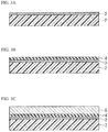
- FIGS. 3A to 3C are cross-sectional views schematically showing steps of manufacturing the multi-layered film according to the embodiment.
- the method of manufacturing a multi-layered film according to the embodiment is the manufacturing method of the multi-layered film 1 that at least includes: a step A of forming the electroconductive layer 3 on the substrate 2 ( FIG. 3A ); a step B of forming the seed layer 4 so as to coat the electroconductive layer 3 ( FIG. 3B ); and a step C of forming the dielectric layer 5 so as to coat the seed layer 4 ( FIG. 3C ).
- the step B the compound including strontium (Sr), ruthenium (Ru), and oxygen (O) is formed as the seed layer by a sputtering method.
- Td substrate temperature
- 560°C ⁇ Td ⁇ 720°C is determined.
- the compound including strontium (Sr), ruthenium (Ru), and oxygen (O) is formed as the seed layer by a sputtering method in the step B, 560°C ⁇ Td ⁇ 720°C is determined in the step C where a substrate temperature is Td (dielectric) when the dielectric layer is formed.
- the dielectric film formed on the seed layer does not include a pyrochlore phase but has a high degree of crystallinity.
- Such multi-layered film has excellent characteristics such as high piezoelectricity and high voltage resistance.
- FIG. 4 is a schematic cross-sectional view showing an example of the internal constitution of a film formation apparatus 10.
- the film formation apparatus 10 includes: a vacuum chamber 11; a target 21; a support (substrate holding stage) 32; a temperature controller 18; a sputtering power source 13; a sputtering gas introduction unit 14; a first adhesion-preventing plate 34; and a second adhesion-preventing plate 35.
- the target 21 is disposed in the vacuum chamber 11.
- the support 32 is disposed at the position facing to the target 21 and is configured to hold a substrate 31 (substrate 2).
- the temperature controller 18 controls a substrate temperature by heating or cooling the substrate 31 supported by the support 32.
- the sputtering power source 13 is configured to apply a voltage to the target 21.
- the sputtering gas introduction unit 14 is configured to introduce a sputtering gas into the vacuum chamber 11.
- the first adhesion-preventing plate 34 and the second adhesion-preventing plate 35 are disposed in the vacuum chamber 11 at the positions to which particles emitted from the target 21 are attached.
- a cathode electrode 22 is disposed at the upper wall surface of the vacuum chamber 11 with an insulating member 28 interposed therebetween, and the cathode electrode 22 is electrically insulated from the vacuum chamber 11.
- the vacuum chamber 11 has a ground potential.
- One of the surfaces of the cathode electrode 22 is locally exposed to the inside of the vacuum chamber 11.
- the target 21 is brought into close contact with and fixed to the center portion of the exposed region of the surface of the cathode electrode 22, and the target 21 is electrically connected to the cathode electrode 22.
- the sputtering power source 13 is disposed outside the vacuum chamber 11.
- the sputtering power source 13 is electrically connected to the cathode electrode 22 and is capable of applying an alternating voltage to the target 21 through the cathode electrode 22.
- a magnet device 29 is disposed on the cathode electrode 22 on the opposite side of the target 21, that is, on the other side of the cathode electrode 22.
- the magnet device 29 is configured to form magnetic field lines on the surface of the target 21.
- the support 32 on which the substrate 31 is to be mounted is made of, for example, carburization silicon (SiC).
- the outer-periphery of the support 32 is formed larger than the outer-periphery of the substrate 31.
- the surface of the support 32 is arranged so as to face the surface of the target 21.
- the means which electrostatically attracts the substrate 31 is located inside the support 32.
- the back surface of the substrate 31 is brought into close contact with the center region of the surface of the support 32, and the substrate 31 is thermally connected to the support 32.
- the first adhesion-preventing plate 34 is made of quartz or ceramics such as alumina.
- the first adhesion-preventing plate 34 is formed in an annular shape such that the inner-periphery of the first adhesion-preventing plate 34 is larger than the outer-periphery of the substrate 31 and the first adhesion-preventing plate is arranged so as to cover the outer-edge portion which is the outside of the center region of the surface of the support 32.
- the back surface of the first adhesion-preventing plate 34 is brought into close contact with the outer-edge portion of the surface of the support 32, and the first adhesion-preventing plate 34 is thermally connected to the support 32.
- the first adhesion-preventing plate 34 is arranged so as to surround the outer side of the outer-periphery of the substrate 31.
- the second adhesion-preventing plate 35 is made of quartz or ceramics such as alumina.
- the second adhesion-preventing plate 35 is formed in a cylindrical shape such that the inner-periphery of the second adhesion-preventing plate 35 is larger than the outer-periphery of the target 21 or the outer-periphery of the substrate 31.
- the second adhesion-preventing plate 35 is arranged between the support 32 and the cathode electrode 22 and is configured to surround the side region of the space between the substrate 31 and the target 21.
- the temperature controller 18 includes a heat generation member 33 and a heating power source 17.
- SiC As a material used to form the heat generation member 33, SiC is used.
- the heat generation member 33 is placed at the position on the opposite side of the substrate 31 with the support 32 interposed therebetween.
- the heating power source 17 is electrically connected to the heat generation member 33.
- the substrate 31 and the first adhesion-preventing plate 34 are thereby heated together.
- the back surface of the substrate 31 is in close contact with the center region of the surface of the support 32, the heat is uniformly transferred to the center portion of the substrate 31 and the outer-edge portion.
- a cooling unit 38 is disposed on the heat generation member 33 on the opposite side of the support 32.
- the cooling unit 38 is configured to be able to circulate a temperature-controlled cooling medium in the internal side thereof and prevents the wall surface of the vacuum chamber 11 from being heated even where heat is generated from the heat generation member 33.
- the sputtering gas introduction unit 14 is connected to the inside of the vacuum chamber 11 and is configured to be able to introduce a sputtering gas into the inside of the vacuum chamber 11.
- FIGS. 3A to 3C are cross-sectional views showing steps of manufacturing the multi-layered film according to the embodiment.
- FIG. 4 shows an example of the case where the film formation apparatus 10 includes one vacuum chamber 11 in order to simplify the explanation thereof; however, in the manufacturing method including the steps A to C which will be described below, the case is explained where the film formation apparatus that is configured to include at least three vacuum chambers 11a, 11b, and 11c (11) is used.
- the vacuum chambers are communicated with each other via an isolation valve which is not shown in the figure in the paperface depth direction in FIG. 4 .
- the vacuum chamber 11a (11) is a vacuum chamber that is used to form an electroconductive layer.
- the vacuum chamber 11b (11) is a vacuum chamber that is used to form a seed layer.
- the vacuum chamber 11c (11) is a vacuum chamber that is used to form a dielectric layer.
- the vacuum chambers are discriminated by reference numerals, and members associated with each vacuum chamber are not discriminated by reference numerals.
- the electroconductive layer 3 made of platinum (Pt) is formed on a main surface of the substrate 2 made of silicon (Si).
- the pressure of the internal space of the vacuum chamber 11a (11) in which a target serving as the target 21 a (21) and made of Pt is disposed is reduced by use of a vacuum pump 15.
- the internal space of the vacuum chamber 11a (11) is in a state of having a high degree of vacuum that is higher than the degree of vacuum atmosphere in which a film is formed.
- the vacuum pumping is continuously carried out and the vacuum atmosphere in the vacuum chamber 11 is thereby maintained.
- the substrate 31 on which a film is to be formed in the internal space of the vacuum chamber 11a (11) is transferred thereto through an inlet which is not shown in the figure.
- the substrate 31 is held on the center region of the support 32 so that the main surface side of the substrate 31 faces the sputtering surface of the target 21.
- the temperature-controlled cooling medium circulates in the cooling unit 38 in advance.
- an Ar gas serving as a sputtering gas is introduced into the inside of the vacuum chamber 11 from the sputtering gas introduction unit 14, an alternating voltage is applied from the sputtering power source 13 to the cathode electrode 22, and Pt target is thereby sputtered.
- the Pt electroconductive layer 3 is formed on the main surface side of the substrate 31.
- the seed layer 4 is formed so as to coat the electroconductive layer 3.
- An oxidative product made of a compound including strontium (Sr), ruthenium (Ru), and oxygen (O) is formed as the seed layer 4.
- An SRO target that is made of an oxidative product including Sr, Ru, and O and serves as the target 21 is disposed in the vacuum chamber 11b (11), the pressure of the internal space of the vacuum chamber is previously reduced by the vacuum pump 15, and in advance, the internal space of the vacuum chamber is in a vacuum state of having a high degree of vacuum that is higher than the degree of vacuum atmosphere in which a film is formed.
- the substrate 31 on which the Pt electroconductive layer 3 is provided in advance is transferred from the vacuum chamber 11a (11) to the internal space of the vacuum chamber 11b (11).
- the substrate 31 is held on the center region of the surface of the support 32 so that the main surface of the substrate 31, that is, the Pt electroconductive layer 3 faces the sputtering surface of the SRO target 21.
- Ar gas and oxygen gas serving as a sputtering gas are introduced into the inside of the vacuum chamber 11b (11) from the sputtering gas introduction unit 14, and the SRO target is sputtered by applying an alternating voltage to the cathode electrode 22 from the sputtering power source 13.
- the seed layer 4 made of SRO is formed on the Pt electroconductive layer 3 located on the main surface side of the substrate 31.
- the substrate temperature in the film formation time is controlled based on a predetermined temperature profile as necessary.
- a constantnt temperature may be maintained from the start of film formation to completion of the film formation.
- the temperature at the start of film formation may be determined to be higher than that of the completion of the film formation.
- the dielectric layer 5 is formed so as to coat the seed layer 4.
- a PZT film serving as the dielectric layer 5 is formed by a sputtering method.
- the substrate temperature Td when forming the dielectric layer 5 is 560°C ⁇ Td ⁇ 720°C.
- a PZT target serving as the target 21 is disposed in the vacuum chamber 11c (11), the pressure of the internal space of the vacuum chamber is reduced by the vacuum pump 15, and the internal space of the vacuum chamber is thereby in a vacuum state of having a high degree of vacuum that is higher than the degree of vacuum atmosphere in which a film is formed.
- the substrate 31 on which the Pt electroconductive layer 3 and the seed layer 4 are provided in advance is transferred from the vacuum chamber 11b (11) to the internal space of the vacuum chamber 11c (11).
- the substrate 31 is held on the center region of the surface of the support 32 so that the main surface of the substrate 31, that is, the seed layer 4 faces the sputtering surface of the PZT target 21.
- the substrate 31 is maintained in a film deposition temperature, an Ar gas and an oxygen gas which serve as a sputtering gas are introduced from the sputtering gas introduction unit 14 to the vacuum chamber 11b (11), an alternating voltage is applied from the sputtering power supply 13 to the cathode electrode 22, and the PZT target is thereby sputtered.
- the dielectric layer 5 formed of the PZT film having the perovskite structure is formed on the seed layer 4 located on the main surface side of the substrate 31.
- the substrate temperature Td when forming the dielectric layer 5 is determined to be in the range of 560°C ⁇ Td ⁇ 720°C.
- the substrate temperature Td is higher than 720°C, it is difficult to limit the generation of a pyrochlore phase.
- the substrate temperature Td to be in the range of 560°C ⁇ Td ⁇ 720°C, formation of a pyrochlore phase is limited, and it is possible to form the dielectric layer 5 having a high degree of crystallinity.
- the substrate temperature in the film formation time is controlled based on a predetermined temperature profile as necessary.
- a constant temperature may be maintained from the start of film formation to completion of the film formation.
- the temperature at the start of film formation may be determined to be higher than that of the completion of the film formation.
- the application of voltage from the sputtering power source 13 to the cathode electrode 22 is stopped, and the introduction of the sputtering gas from the sputtering gas introduction unit 14 into the inside of the vacuum chamber 11c (11) is stopped.
- the supply of the electrical current from the heating power source 17 to the heat generation member 33 is stopped, the heat generation member 33 is cooled down, and the temperature of the substrate 31 becomes lower than the film deposition temperature.
- the temperature of the heat generation member 33 is reduced to be lower than or equal to 400°C, and the temperature is maintained.
- the film-formed substrate 31 on which the multi-layered film is formed by stacking the three layers (the electroconductive layer, the seed layer, and the dielectric layer) in order is discharged to the outside of the vacuum chamber 11 through an outlet which is not shown in the figure.
- a transfer robot which is not shown in the figure is preferably used to transfer the aforementioned substrate, that is, transfer the substrate from the outside to the vacuum chamber 11a (11), transfer the substrate between the vacuum chambers, transfer the substrate from the vacuum chamber 11c (11) to the outside.
- the multi-layered film 1 having the structure shown in FIG. 1 is manufactured.
- the dielectric layer 5 does not include a pyrochlore phase but has a high degree of crystallinity.
- the multi-layered film 1 realizes, for example, both high piezoelectricity and high voltage resistance, and has excellent characteristics.
- the above-described multi-layered film 1 is preferably used in, for example, a piezo element or the like.
- PZT films (dielectric layer) are formed with or without a seed layer, and the characteristics thereof are evaluated.
- a multi-layered film was formed by stacking an electroconductive layer formed of a Pt film, a seed layer formed of an SrRuO 3 (SRO) film, and a dielectric layer formed of a PZT film in order.
- SRO SrRuO 3
- a silicon (Si) wafer having a diameter of eight inches was used as the substrate.
- a Si wafer which has a main surface side on which a thermal oxidation film (SiO 2 film), a Ti film functioning as an adhesion layer (thickness of 20 nm), and a Pt film functioning as a lower electrode layer (thickness of 100 nm) are layered in order in advance.
- a thermal oxidation film SiO 2 film
- Ti film functioning as an adhesion layer
- Pt film functioning as a lower electrode layer
- a flat-plate magnetron sputtering apparatus (SME-200) having the configuration shown in FIG. 4 was used.
- a high-frequency power source (frequency of 13.56 MHz) was used.
- the conditions of forming the seed layer formed of the SrRuO 3 film were determined as follows.
- an SrRuO 3 target having a diameter of 300 mm and a thickness of 5 mm was used as a target.
- a sputtering power was 0.7 (kW)
- a sputtering pressure was 0.4 (Pa)
- a substrate temperature was 530°C to 740°C.
- the film thickness of the seed layer was 100 (nm).
- the conditions of forming the dielectric layer formed of the PZT film were determined as follows.
- a PZT target having a diameter of 300 mm and a thickness of 5 mm was used.
- a sputtering power was 2.5 (kW)
- a sputtering pressure was 0.5 (Pa)
- a substrate temperature was 720°C.
- the film thickness of the dielectric layer was 2.0 ( ⁇ m).
- Sample 1 The sample of the experimental example 1 which is manufactured under the aforementioned conditions was referred to as Sample 1.
- a multi-layered film was formed by forming a PZT film on a Pt thin film on a substrate without providing a seed layer.
- a PZT film is formed under the substrate temperature condition of 585°C.
- the conditions of forming the films other than the dielectric layer formed of the PZT film are the same as that of the experimental example 1.
- Sample 2 The sample of the experimental example 2 which is manufactured under the aforementioned conditions was referred to as Sample 2.
- a PZT film was formed on a Pt thin film of a Si substrate without forming a seed layer at a substrate temperature of 625°C, and a multi-layered film is thereby formed.
- Sample 3 The sample of the experimental example 3 which is manufactured under the aforementioned conditions was referred to as Sample 3.
- a PZT film was formed on a Pt thin film of a Si substrate without forming a seed layer at a substrate temperature of 665°C, and a multi-layered film is thereby formed.
- Sample 4 The sample of the experimental example 4 which is manufactured under the aforementioned conditions was referred to as Sample 4.
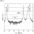
- FIG. 5 shows an X-ray chart representing Sample 1 (seed layer: SrRuO 3 film).
- FIG. 6 shows an X-ray chart representing Samples 2 to 4 (absence of a seed layer).
- the PZT films were formed in the case where a substrate temperature when forming a film varies in the range of 530°C to 740°C, and the crystal structure was analyzed for each of the PZT films which are formed at various substrate temperatures.
- the PZT film is formed without forming the seed layer in Samples 2 to 4, and a peak due to a pyrochlore phase (two peaks surrounded by ellipses in FIG. 6 ) of Sample 4 in which the film deposition temperature is 665°C was observed from FIG. 6 .
- FIG. 7 is a chart showing the relationship between a substrate temperature and peak intensity due to a pyrochlore phase.
- the PZT film has a pyrochlore phase serving as a different phase in the case where the substrate temperature is 740°C.
- SRO SrRuO 3
- the PZT film can be formed at a temperature in the range of, for example, 560°C ⁇ Td ⁇ 720°C (substrate temperature), which has a perovskite phase (that forms a crystal structure as a main component) in which a pyrochlore phase serving as a different phase is absent (which is extremely limited to be lower than the back ground in the X-ray chart).
- FIG. 8 is an X-ray chart showing crystallinities of the PZT films of Sample 1 (solid line) and Sample 3 (dotted line).
- the peak thereof has a sharp shape; in the case where a crystallite is small, the width of the peak becomes broader.
- the half-value width (FWHM) of the X-ray diffraction peak due to the (100) of Pb(Zr, Ti)O 3 can be less than or equal to 1 degree.
- the invention is widely applicable to a method of manufacturing a multi-layered film, and a multi-layered film.
Landscapes
- Chemical & Material Sciences (AREA)
- Organic Chemistry (AREA)
- Engineering & Computer Science (AREA)
- Chemical Kinetics & Catalysis (AREA)
- Materials Engineering (AREA)
- Mechanical Engineering (AREA)
- Metallurgy (AREA)
- Inorganic Chemistry (AREA)
- Manufacturing & Machinery (AREA)
- Ceramic Engineering (AREA)
- Physical Vapour Deposition (AREA)
Abstract
Description
- The present invention relates to a method of manufacturing a multi-layered film including a dielectric layer having a high degree of crystallinity and relates to the multi-layered film.
- This application claims priority from Japanese Patent Application No.
2014-127468 filed on June 20, 2014 - Currently, a piezo element using a ferroelectric material such as lead zirconate titanate (Pb(Zr, Ti)O3: PZT) is applied to an MEMS (Micro Electro Mechanical Systems) technique such as an inkjet head an acceleration sensor.
- Particularly, a PZT film has been attracted attention and actively researched by various organizations (
Patent Document 1 to 3). - Various research has been conducted in order to improve withstand voltage characteristics of a PZT film.
- In the case of forming a PZT film by a sputtering method, since the film is not sufficiently crystallized when the film formation is completed, there is a need to carry out a heat treatment in order for crystallization after film formation.
- Generally, this heat treatment is referred to as a post- heat treatment or an annealing treatment.
- The crystal of the PZT film includes not only a perovskite phase having requested piezoelectricity but also a pyrochlore phase that is a quasi-stable phase and does not have piezoelectricity.
- Conventionally, a crystal including a pyrochlore phase is easily obtained, but it is extremely difficult to obtain a dielectric film that does not include a pyrochlore phase but has a high degree of crystallinity.
- Consequently, in order to improve the withstand voltage characteristics, the development of the method has been expected which stably forms a multi-layered film provided with the dielectric film that does not include a pyrochlore phase but has a high degree of crystallinity.
-
- [Patent Document 1] Japanese Unexamined Patent Application, First Publication No.
2007-327106 - [Patent Document 2] Japanese Unexamined Patent Application, First Publication No.
2010-084180 - [Patent Document 3] Japanese Unexamined Patent Application, First Publication No.
2003-081694 - The invention was made in view of the above-described conventional situations, and has a first object to provide a method of manufacturing a multi-layered film provided with a dielectric layer that does not include a pyrochlore phase but has a high degree of crystall in ity.
- Furthermore, the invention has a second object to provide a multi-layered film provided with a dielectric layer that does not include a pyrochlore phase but has a high degree of crystallinity.
- According to a first aspect of the invention, a method of manufacturing a multi-layered film, includes: forming an electroconductive layer on a substrate (step A); forming a seed layer by compound including strontium (Sr), ruthenium (Ru), and oxygen (O) so as to coat the electroconductive layer by a sputtering method (step B); and forming a dielectric layer so as to coat the seed layer (step C) so that, where a substrate temperature is defined by Td (dielectric) when the dielectric layer is formed, 560°C≤Td≤720°C is satisfied.
- In the above-described method of manufacturing a multi-layered film of the first aspect, according to the second aspect of the invention, when the dielectric layer is formed, a compound including lead (Pb), zirconia (Zr), titanium (Ti), and oxygen (O) may be formed as the dielectric layer by a sputtering method.
- According to a third aspect of the invention, a multi-layered film includes an electroconductive layer made of platinum (Pt), a seed layer, and a dielectric layer, which are at least sequentially disposed on a main surface of a substrate made of silicon, wherein the seed layer is made of a compound including strontium (Sr), ruthenium (Ru), and oxygen (O), the dielectric layer is made of a compound including lead (Pb), zirconia (Zr), titanium (Ti), and oxygen (O), and the compound that forms the dielectric layer does not have an X-ray diffraction peak due to a pyrochlore phase.
- In the above-described multi-layered film of the third aspect, according to the fourth aspect of the invention, in the compound that forms the dielectric layer, a half-value width (FWHM) of an X-ray diffraction peak due to (100) of Pb(Zr, Ti)O3 may be less than or equal to 1 degree.
- In the method of manufacturing a multi-layered film according to each of the aforementioned aspects, the compound including strontium (Sr), ruthenium (Ru), and oxygen (O) is formed as the seed layer by a sputtering method in the step B, the substrate temperature Td (dielectric) is in the range of 560°C to 720°C when the dielectric layer is formed in the step C, and therefore the dielectric film formed on the seed layer has a high degree of crystallinity.
- Particularly, from the compound that forms the dielectric layer, an X-ray diffraction peak due to a perovskite phase is observed, but an X-ray diffraction peak due to a pyrochlore phase is not observed.
- Accordingly, the invention can provide a method of manufacturing a multi-layered film provided with a dielectric layer that does not include a pyrochlore phase but has a high degree of crystallinity.
- Additionally, in the multi-layered film according to each of the aforementioned aspects, the dielectric layer is made of a compound including lead (Pb), zirconia (Zr), titanium (Ti), and oxygen (O), and the compound that forms the dielectric layer does not include an X-ray diffraction peak due to a pyrochlore phase.
- Therefore, according to the invention, it is possible to provide a multi-layered film including the dielectric layer having a high degree of crystallinity.
- Such multi-layered film has excellent characteristics such as having both high piezoelectricity and high voltage resistance.
-
-
FIG. 1 is a cross-sectional view showing one configuration example of a multi-layered film according to one embodiment of the invention. -
FIG. 2A is a diagram schematically showing the size of a crystallite and the shape of an X-ray diffraction peak. -
FIG. 2B is a diagram schematically showing the size of a crystallite and the shape of an X-ray diffraction peak. -
FIG. 3A is a cross-sectional view showing a process of manufacturing the multi-layered film according to the embodiment. -
FIG. 3B is a cross-sectional view showing a process of manufacturing the multi-layered film according to the embodiment. -
FIG. 3C is a cross-sectional view showing a process of manufacturing the multi-layered film according to the embodiment. -
FIG. 4 is a view schematically showing an internal constitution of a film formation apparatus used in the embodiment. -
FIG. 5 is a chart showing the diffraction peak which indicates the crystal structure of the PZT film formed bySample 1. -
FIG. 6 is a chart showing the diffraction peaks which indicate the crystal structure of the PZT films ofSamples 2 to 4. -
FIG. 7 is a chart showing the relationship between a substrate temperature and peak intensity due to a pyrochlore phase. -
FIG. 8 is a chart showing crystallinities of the PZT films ofSamples - Hereinafter, a multi-layered according to one embodiment of the invention will be described with reference to drawings.
-
FIG. 1 is a cross-sectional view showing one configuration example of a multi-layered film according to the embodiment. - The
multi-layered film 1 includes anelectroconductive layer 3 made of platinum (Pt), aseed layer 4, and a dielectric layer 5 which are at least sequentially disposed on a main surface of asubstrate 2 made of silicon. - The
seed layer 4 is made of a compound including strontium (Sr), ruthenium (Ru), and oxygen (O). - As the
seed layer 4, for example, SrRuO3 (SRO) is adopted. - The dielectric layer 5 is disposed on the above-mentioned
seed layer 4 including strontium (Sr), ruthenium (Ru), and oxygen (O). - The dielectric layer 5 is not particularly limited, but is made of a ferroelectric material such as lead zirconate titanate (Pb(ZrxTi1-x)O3: PZT), PbTiO3, BaTiO3, PMM-PZT, PNN-PZT, PMN-PZT, PNN-PT, PLZT, PZTN, NBT, and KNN
- Particularly, in the
multi-layered film 1 according to the embodiment, a compound forming a dielectric layer has a high degree of crystallinity. - Specifically, since a peak due to a pyrochlore phase is not observed from the compound that forms the dielectric layer by an X-ray diffraction method, the compound does not include a pyrochlore phase.
- Since the
seed layer 4 has, for example, a perovskite structure, the dielectric layer 5 disposed on theseed layer 4 has a perovskite structure which does not include a different phase. - Consequently, the
multi-layered film 1 has excellent characteristics such as high piezoelectricity and high voltage resistance. - The above-described
multi-layered film 1 is preferably used in, for example, a piezo element or the like. - Moreover, in the compound forming the dielectric layer 5, the half-value width (full width at half maximum: FWHM) of the X-ray diffraction peak which is caused by Pb(ZrxTi1-x)O3 (100) is less than or equal to 1 degree.
- Here, according to P. Scherrer (Kazuhiko Kandori, "Study of solid-state structure by powder X-ray diffraction measurement", online, searched on the Internet on March 10, 2014 (URL: http://www.osaka-kyoiku.ac.jp/~rck/kandori.pdf), where the size of a crystallite (crystallite diameter) is represented as L and where the broadening at the position corresponding to a half of the peak intensity is represented as 20 (half-value width, β), the relationship of "L=Kλ/(βcosθ)" is obtained.
-
FIGS. 2A and 2B are diagrams schematically showing the size of a crystallite and the shape of an X-ray diffraction peak. - As shown in
FIG. 2A , in the case where a crystallite grows well, a half-value width is narrow, and a peak having a sharp shape is observed. - In contrast, as shown in
FIG. 2B , in the case where a crystallite is small, a half-value width is widened, and a peak having a dull shape is observed. - According to the above evaluation method, it is apparent that, in the compound forming the dielectric layer 5 which constitutes the multi-layered film according to the embodiment and in which the aforementioned half-value width of 1 degree or less is observed, the crystallite is largely grown and has an extremely high degree of crystallinity.
- As a result of adopting the method of manufacturing a multi-layered film according to the embodiment which will be described later, the dielectric film formed on the
seed layer 4 including strontium (Sr), ruthenium (Ru), and oxygen (O) does not include a pyrochlore phase but has a high degree of crystallinity. - The
multi-layered film 1 has excellent characteristics such as high piezoelectricity and high voltage resistance. - The above-described
multi-layered film 1 is preferably used in, for example, a piezo element or the like. - Hereinbelow, a method of manufacturing the multi-layered film according to the embodiment will be described.
-
FIGS. 3A to 3C are cross-sectional views schematically showing steps of manufacturing the multi-layered film according to the embodiment. - The method of manufacturing a multi-layered film according to the embodiment is the manufacturing method of the
multi-layered film 1 that at least includes: a step A of forming theelectroconductive layer 3 on the substrate 2 (FIG. 3A ); a step B of forming theseed layer 4 so as to coat the electroconductive layer 3 (FIG. 3B ); and a step C of forming the dielectric layer 5 so as to coat the seed layer 4 (FIG. 3C ). In the step B, the compound including strontium (Sr), ruthenium (Ru), and oxygen (O) is formed as the seed layer by a sputtering method. In the step C, where a substrate temperature is Td (dielectric) when the dielectric layer is formed, 560°C≤Td≤720°C is determined. - In the method of manufacturing the multi-layered film according to the embodiment, the compound including strontium (Sr), ruthenium (Ru), and oxygen (O) is formed as the seed layer by a sputtering method in the step B, 560°C≤Td≤720°C is determined in the step C where a substrate temperature is Td (dielectric) when the dielectric layer is formed.
- Consequently, the dielectric film formed on the seed layer does not include a pyrochlore phase but has a high degree of crystallinity.
- Such multi-layered film has excellent characteristics such as high piezoelectricity and high voltage resistance.
- In the following explanation, as an example, the case will be described where lead zirconate titanate (Pb(ZrxTi1-x)O3: PZT) is used as the dielectric layer 5; however, the invention is not limited to this.
- Hereinbelow, the configuration of a preferred film formation apparatus in order to carry out the method of manufacturing a multi-layered film according to the embodiment will be described.
-
FIG. 4 is a schematic cross-sectional view showing an example of the internal constitution of afilm formation apparatus 10. - The
film formation apparatus 10 includes: avacuum chamber 11; atarget 21; a support (substrate holding stage) 32; atemperature controller 18; asputtering power source 13; a sputteringgas introduction unit 14; a first adhesion-preventingplate 34; and a second adhesion-preventingplate 35. - The
target 21 is disposed in thevacuum chamber 11. - The
support 32 is disposed at the position facing to thetarget 21 and is configured to hold a substrate 31 (substrate 2). - The
temperature controller 18 controls a substrate temperature by heating or cooling thesubstrate 31 supported by thesupport 32. - The sputtering
power source 13 is configured to apply a voltage to thetarget 21. - The sputtering
gas introduction unit 14 is configured to introduce a sputtering gas into thevacuum chamber 11. - The first adhesion-preventing
plate 34 and the second adhesion-preventingplate 35 are disposed in thevacuum chamber 11 at the positions to which particles emitted from thetarget 21 are attached. - A
cathode electrode 22 is disposed at the upper wall surface of thevacuum chamber 11 with an insulatingmember 28 interposed therebetween, and thecathode electrode 22 is electrically insulated from thevacuum chamber 11. - The
vacuum chamber 11 has a ground potential. - One of the surfaces of the
cathode electrode 22 is locally exposed to the inside of thevacuum chamber 11. - The
target 21 is brought into close contact with and fixed to the center portion of the exposed region of the surface of thecathode electrode 22, and thetarget 21 is electrically connected to thecathode electrode 22. - The sputtering
power source 13 is disposed outside thevacuum chamber 11. - The sputtering
power source 13 is electrically connected to thecathode electrode 22 and is capable of applying an alternating voltage to thetarget 21 through thecathode electrode 22. - A
magnet device 29 is disposed on thecathode electrode 22 on the opposite side of thetarget 21, that is, on the other side of thecathode electrode 22. - The
magnet device 29 is configured to form magnetic field lines on the surface of thetarget 21. - The
support 32 on which thesubstrate 31 is to be mounted is made of, for example, carburization silicon (SiC). - The outer-periphery of the
support 32 is formed larger than the outer-periphery of thesubstrate 31. - The surface of the
support 32 is arranged so as to face the surface of thetarget 21. - The means which electrostatically attracts the
substrate 31 is located inside thesupport 32. - When the
substrate 31 is electrostatically attracted to the center region of the surface of thesupport 32, the back surface of thesubstrate 31 is brought into close contact with the center region of the surface of thesupport 32, and thesubstrate 31 is thermally connected to thesupport 32. - The first adhesion-preventing
plate 34 is made of quartz or ceramics such as alumina. - The first adhesion-preventing
plate 34 is formed in an annular shape such that the inner-periphery of the first adhesion-preventingplate 34 is larger than the outer-periphery of thesubstrate 31 and the first adhesion-preventing plate is arranged so as to cover the outer-edge portion which is the outside of the center region of the surface of thesupport 32. - Consequently, the particles discharged from the
target 21 are prevented from being adhered to the outer-edge portion of the surface of thesupport 32. - The back surface of the first adhesion-preventing
plate 34 is brought into close contact with the outer-edge portion of the surface of thesupport 32, and the first adhesion-preventingplate 34 is thermally connected to thesupport 32. - When the
substrate 31 is mounted on the center region of the surface of thesupport 32, the first adhesion-preventingplate 34 is arranged so as to surround the outer side of the outer-periphery of thesubstrate 31. - The second adhesion-preventing
plate 35 is made of quartz or ceramics such as alumina. - The second adhesion-preventing
plate 35 is formed in a cylindrical shape such that the inner-periphery of the second adhesion-preventingplate 35 is larger than the outer-periphery of thetarget 21 or the outer-periphery of thesubstrate 31. - The second adhesion-preventing
plate 35 is arranged between thesupport 32 and thecathode electrode 22 and is configured to surround the side region of the space between thesubstrate 31 and thetarget 21. - For this reason, the particles discharged from the
target 21 are prevented from being adhered to the wall surface of thevacuum chamber 11. - The
temperature controller 18 includes a heat generation member 33 and aheating power source 17. - As a material used to form the heat generation member 33, SiC is used.
- The heat generation member 33 is placed at the position on the opposite side of the
substrate 31 with thesupport 32 interposed therebetween. - The
heating power source 17 is electrically connected to the heat generation member 33. - When a direct current is supplied to the heat generation member 33 from the
heating power source 17, the heat generated from the heat generation member 33 is transmitted through thesupport 32 to thesubstrate 31 mounted on thesupport 32 and the first adhesion-preventingplate 34. - Therefore, the
substrate 31 and the first adhesion-preventingplate 34 are thereby heated together. - The back surface of the
substrate 31 is in close contact with the center region of the surface of thesupport 32, the heat is uniformly transferred to the center portion of thesubstrate 31 and the outer-edge portion. - A cooling unit 38 is disposed on the heat generation member 33 on the opposite side of the
support 32. - The cooling unit 38 is configured to be able to circulate a temperature-controlled cooling medium in the internal side thereof and prevents the wall surface of the
vacuum chamber 11 from being heated even where heat is generated from the heat generation member 33. - The sputtering
gas introduction unit 14 is connected to the inside of thevacuum chamber 11 and is configured to be able to introduce a sputtering gas into the inside of thevacuum chamber 11. - Hereinbelow, a method of forming a multi-layered film will be described.
-
FIGS. 3A to 3C are cross-sectional views showing steps of manufacturing the multi-layered film according to the embodiment. - When such manufacturing processes are carried out, the aforementioned film formation apparatus shown in
FIG. 4 is used. -
FIG. 4 shows an example of the case where thefilm formation apparatus 10 includes onevacuum chamber 11 in order to simplify the explanation thereof; however, in the manufacturing method including the steps A to C which will be described below, the case is explained where the film formation apparatus that is configured to include at least three vacuum chambers 11a, 11b, and 11c (11) is used. The vacuum chambers are communicated with each other via an isolation valve which is not shown in the figure in the paperface depth direction inFIG. 4 . - Here, the vacuum chamber 11a (11) is a vacuum chamber that is used to form an electroconductive layer.
- The vacuum chamber 11b (11) is a vacuum chamber that is used to form a seed layer.
- The vacuum chamber 11c (11) is a vacuum chamber that is used to form a dielectric layer.
- In the following explanation, the vacuum chambers are discriminated by reference numerals, and members associated with each vacuum chamber are not discriminated by reference numerals.
- As shown in
FIG. 3A , theelectroconductive layer 3 made of platinum (Pt) is formed on a main surface of thesubstrate 2 made of silicon (Si). - Hereinbelow, the case of directly forming an electroconductive layer on the main surface side of the substrate will be described; however, if required, before forming the electroconductive layer, the other film may be provided on the main surface side of the
substrate 2. - The pressure of the internal space of the vacuum chamber 11a (11) in which a target serving as the target 21 a (21) and made of Pt is disposed is reduced by use of a
vacuum pump 15. - Consequently, the internal space of the vacuum chamber 11a (11) is in a state of having a high degree of vacuum that is higher than the degree of vacuum atmosphere in which a film is formed.
- After that, the vacuum pumping is continuously carried out and the vacuum atmosphere in the
vacuum chamber 11 is thereby maintained. - While maintaining the vacuum atmosphere in the
vacuum chamber 11, thesubstrate 31 on which a film is to be formed in the internal space of the vacuum chamber 11a (11) is transferred thereto through an inlet which is not shown in the figure. - Subsequently, the
substrate 31 is held on the center region of thesupport 32 so that the main surface side of thesubstrate 31 faces the sputtering surface of thetarget 21. - The temperature-controlled cooling medium circulates in the cooling unit 38 in advance.
- Next, in a step of forming an electroconductive layer, while the
substrate 31 is maintained in a film deposition temperature, an Ar gas serving as a sputtering gas is introduced into the inside of thevacuum chamber 11 from the sputteringgas introduction unit 14, an alternating voltage is applied from the sputteringpower source 13 to thecathode electrode 22, and Pt target is thereby sputtered. - Consequently, the
Pt electroconductive layer 3 is formed on the main surface side of thesubstrate 31. - As shown in
FIG. 3B , theseed layer 4 is formed so as to coat theelectroconductive layer 3. - By use of a sputtering method, An oxidative product made of a compound including strontium (Sr), ruthenium (Ru), and oxygen (O) is formed as the
seed layer 4. - An SRO target that is made of an oxidative product including Sr, Ru, and O and serves as the
target 21 is disposed in the vacuum chamber 11b (11), the pressure of the internal space of the vacuum chamber is previously reduced by thevacuum pump 15, and in advance, the internal space of the vacuum chamber is in a vacuum state of having a high degree of vacuum that is higher than the degree of vacuum atmosphere in which a film is formed. - While maintaining the vacuum atmosphere in the vacuum chamber 11b (11), the
substrate 31 on which thePt electroconductive layer 3 is provided in advance is transferred from the vacuum chamber 11a (11) to the internal space of the vacuum chamber 11b (11). - Subsequently, the
substrate 31 is held on the center region of the surface of thesupport 32 so that the main surface of thesubstrate 31, that is, thePt electroconductive layer 3 faces the sputtering surface of theSRO target 21. - After that, while maintaining the
substrate 31 at a film deposition temperature, Ar gas and oxygen gas serving as a sputtering gas are introduced into the inside of the vacuum chamber 11b (11) from the sputteringgas introduction unit 14, and the SRO target is sputtered by applying an alternating voltage to thecathode electrode 22 from the sputteringpower source 13. - Consequently, the
seed layer 4 made of SRO is formed on thePt electroconductive layer 3 located on the main surface side of thesubstrate 31. - Particularly, in the case of forming the
seed layer 4, the substrate temperature in the film formation time is controlled based on a predetermined temperature profile as necessary. - A constatnt temperature may be maintained from the start of film formation to completion of the film formation.
- For example, the temperature at the start of film formation may be determined to be higher than that of the completion of the film formation.
- As shown in
FIG. 3C , the dielectric layer 5 is formed so as to coat theseed layer 4. - In the step C, a PZT film serving as the dielectric layer 5 is formed by a sputtering method.
- Here, in the step C, the substrate temperature Td when forming the dielectric layer 5 is 560°C≤Td≤720°C.
- A PZT target serving as the
target 21 is disposed in the vacuum chamber 11c (11), the pressure of the internal space of the vacuum chamber is reduced by thevacuum pump 15, and the internal space of the vacuum chamber is thereby in a vacuum state of having a high degree of vacuum that is higher than the degree of vacuum atmosphere in which a film is formed. - While maintaining the vacuum atmosphere in the vacuum chamber 11c (11), the
substrate 31 on which thePt electroconductive layer 3 and theseed layer 4 are provided in advance is transferred from the vacuum chamber 11b (11) to the internal space of the vacuum chamber 11c (11). - Subsequently, the
substrate 31 is held on the center region of the surface of thesupport 32 so that the main surface of thesubstrate 31, that is, theseed layer 4 faces the sputtering surface of thePZT target 21. - Next, the
substrate 31 is maintained in a film deposition temperature, an Ar gas and an oxygen gas which serve as a sputtering gas are introduced from the sputteringgas introduction unit 14 to the vacuum chamber 11b (11), an alternating voltage is applied from the sputteringpower supply 13 to thecathode electrode 22, and the PZT target is thereby sputtered. - Accordingly, the dielectric layer 5 formed of the PZT film having the perovskite structure is formed on the
seed layer 4 located on the main surface side of thesubstrate 31. - The substrate temperature Td when forming the dielectric layer 5 is determined to be in the range of 560°C≤Td≤720°C.
- In the case where the substrate temperature Td is lower than 560°C, growth of the crystallite does not sufficiently proceed.
- In the case where the substrate temperature Td is higher than 720°C, it is difficult to limit the generation of a pyrochlore phase.
- Accordingly, as a result of determining the substrate temperature Td to be in the range of 560°C≤Td≤720°C, formation of a pyrochlore phase is limited, and it is possible to form the dielectric layer 5 having a high degree of crystallinity.
- Particularly, in the case of forming the dielectric layer 5, the substrate temperature in the film formation time is controlled based on a predetermined temperature profile as necessary.
- A constant temperature may be maintained from the start of film formation to completion of the film formation.
- For example, the temperature at the start of film formation may be determined to be higher than that of the completion of the film formation.
- As described hereinbelow, as compared with a conventional layered structure in which a seed layer is not provided (electroconductive layer/a dielectric layer), it is possible to limit the formation of a pyrochlore phase by employing a SRO film as the
seed layer 4. - After the PZT thin film having a predetermined film thickness is formed on the
substrate 31, the application of voltage from the sputteringpower source 13 to thecathode electrode 22 is stopped, and the introduction of the sputtering gas from the sputteringgas introduction unit 14 into the inside of the vacuum chamber 11c (11) is stopped. - The supply of the electrical current from the
heating power source 17 to the heat generation member 33 is stopped, the heat generation member 33 is cooled down, and the temperature of thesubstrate 31 becomes lower than the film deposition temperature. - For example, in the vacuum chamber 11c (11), the temperature of the heat generation member 33 is reduced to be lower than or equal to 400°C, and the temperature is maintained.
- While maintaining the vacuum atmosphere in the
vacuum chamber 11, the film-formedsubstrate 31 on which the multi-layered film is formed by stacking the three layers (the electroconductive layer, the seed layer, and the dielectric layer) in order is discharged to the outside of thevacuum chamber 11 through an outlet which is not shown in the figure. - Particularly, a transfer robot which is not shown in the figure is preferably used to transfer the aforementioned substrate, that is, transfer the substrate from the outside to the vacuum chamber 11a (11), transfer the substrate between the vacuum chambers, transfer the substrate from the vacuum chamber 11c (11) to the outside.
- In the above manner, the
multi-layered film 1 having the structure shown inFIG. 1 is manufactured. - In the
multi-layered film 1, the dielectric layer 5 does not include a pyrochlore phase but has a high degree of crystallinity. - Consequently, the
multi-layered film 1 realizes, for example, both high piezoelectricity and high voltage resistance, and has excellent characteristics. - The above-described
multi-layered film 1 is preferably used in, for example, a piezo element or the like. - Hereinbelow, examples of experiment will be described which are carried out in order to check the effect of the above-described invention.
- PZT films (dielectric layer) are formed with or without a seed layer, and the characteristics thereof are evaluated.
- In this example, a multi-layered film was formed by stacking an electroconductive layer formed of a Pt film, a seed layer formed of an SrRuO3 (SRO) film, and a dielectric layer formed of a PZT film in order.
- As the substrate, a silicon (Si) wafer having a diameter of eight inches was used.
- Here, a Si wafer was used which has a main surface side on which a thermal oxidation film (SiO2 film), a Ti film functioning as an adhesion layer (thickness of 20 nm), and a Pt film functioning as a lower electrode layer (thickness of 100 nm) are layered in order in advance.
- As a sputtering apparatus, a flat-plate magnetron sputtering apparatus (SME-200) having the configuration shown in
FIG. 4 was used. - As a sputtering power source, a high-frequency power source (frequency of 13.56 MHz) was used.
- The conditions of forming the seed layer formed of the SrRuO3 film were determined as follows.
- As a target, an SrRuO3 target having a diameter of 300 mm and a thickness of 5 mm was used.
- A sputtering power was 0.7 (kW), a sputtering pressure was 0.4 (Pa), and a substrate temperature was 530°C to 740°C.
- The film thickness of the seed layer was 100 (nm).
- The conditions of forming the dielectric layer formed of the PZT film were determined as follows.
- As a target, a PZT target having a diameter of 300 mm and a thickness of 5 mm was used.
- A sputtering power was 2.5 (kW), a sputtering pressure was 0.5 (Pa), and a substrate temperature was 720°C.
- The film thickness of the dielectric layer was 2.0 (µm).
- The sample of the experimental example 1 which is manufactured under the aforementioned conditions was referred to as
Sample 1. - In this example, a multi-layered film was formed by forming a PZT film on a Pt thin film on a substrate without providing a seed layer.
- A PZT film is formed under the substrate temperature condition of 585°C.
- The conditions of forming the films other than the dielectric layer formed of the PZT film are the same as that of the experimental example 1.
- The sample of the experimental example 2 which is manufactured under the aforementioned conditions was referred to as
Sample 2. - In this example, a PZT film was formed on a Pt thin film of a Si substrate without forming a seed layer at a substrate temperature of 625°C, and a multi-layered film is thereby formed.
- The conditions of forming the films other than the PZT film are the same as that of the
aforementioned Sample 1. - The sample of the experimental example 3 which is manufactured under the aforementioned conditions was referred to as
Sample 3. - In this example, a PZT film was formed on a Pt thin film of a Si substrate without forming a seed layer at a substrate temperature of 665°C, and a multi-layered film is thereby formed.
- The conditions of forming the films other than the PZT film are the same as that of the
aforementioned Sample 1. - The sample of the experimental example 4 which is manufactured under the aforementioned conditions was referred to as
Sample 4. - The crystal structures of the PZT films of
Samples 1 to 4 which are manufactured in the experimental examples 1 to 4, respectively, were analyzed by use of an X-ray diffraction method. -
FIG. 5 shows an X-ray chart representing Sample 1 (seed layer: SrRuO3 film). - Additionally,
FIG. 6 shows an X-raychart representing Samples 2 to 4 (absence of a seed layer). - In
Sample 1, the PZT films were formed in the case where a substrate temperature when forming a film varies in the range of 530°C to 740°C, and the crystal structure was analyzed for each of the PZT films which are formed at various substrate temperatures. - The PZT film is formed without forming the seed layer in
Samples 2 to 4, and a peak due to a pyrochlore phase (two peaks surrounded by ellipses inFIG. 6 ) ofSample 4 in which the film deposition temperature is 665°C was observed fromFIG. 6 . -
FIG. 7 is a chart showing the relationship between a substrate temperature and peak intensity due to a pyrochlore phase. - It was observed from
FIG. 7 that, inSample 1 in which the seed layer made of an SrRuO3 film is formed, the PZT film has a pyrochlore phase serving as a different phase in the case where the substrate temperature is 740°C. - In the case of the other substrate temperatures (560°C to 720°C), a pyrochlore phase is not observed.
- That is, it is apparent that, as a result of adopting the configuration using an SrRuO3 film as a seed layer, a PZT film that does not include a pyrochlore phase is obtained in the range of 560°C≤Td≤720°C.
- In the PZT film that is formed on the seed layer formed of the SrRuO3 film, a pyrochlore phase serving as a different phase was not observed when a boundary face is initially formed.
- The reason is believed to be that, since SrRuO3 (SRO) has the coefficient of thermal expansion greater than that of the PZT, the PZT film receives a compression stress in a cooling process, and as a result, the PZT film is oriented in the c-axis.
- Because of this, it was determined that, as a result of using a SrRuO3 film as a seed layer, the PZT film can be formed at a temperature in the range of, for example, 560°C≤Td≤720°C (substrate temperature), which has a perovskite phase (that forms a crystal structure as a main component) in which a pyrochlore phase serving as a different phase is absent (which is extremely limited to be lower than the back ground in the X-ray chart).
-
FIG. 8 is an X-ray chart showing crystallinities of the PZT films of Sample 1 (solid line) and Sample 3 (dotted line). - From
Sample 1, it was observed that, even in the case of using poly PZT, a half-value width of a (100) rocking curve is 0.55 degrees, and it has an extremely higher degree of crystallinity than that of Sample 3 (a half-value width of 4.05 degrees). - That is, as described above, in the case where a crystallite grows well, the peak thereof has a sharp shape; in the case where a crystallite is small, the width of the peak becomes broader.
- In
Sample 3, a pyrochlore phase is prevented from being generated; however, a half-value width of the peak becomes wider, such as 4.05 degrees, and the crystallite can be said to be small. - From
Sample 1, it was observed that the crystallite largely grows and has an extremely higher degree of crystallinity than that ofSample 3. - Particularly, regarding
Sample 1, half-value widths (FWHM) of (100) rocking curves at the nine points on the entire area of the 8-inch wafer were measured. - As a result, it was observed that the half-value widths (FWHM) at the nine points are in the range of 0.52 to 0.59.
- Accordingly, it was determined that, in the compound forming the dielectric layer manufactured by the manufacturing conditions of
Sample 1, the half-value width (FWHM) of the X-ray diffraction peak due to the (100) of Pb(Zr, Ti)O3 can be less than or equal to 1 degree. - It was determined from the above results that it is possible to form the PZT film that does not include a pyrochlore phase but has a high degree of crystallinity by forming a PZT film on the seed layer made of an SrRuO3 (SRO) film at a temperature in the range of 560°C≤Td≤720°C.
- While preferred embodiments of the invention have been described and illustrated above, the invention is not limited to the embodiments.
- Various modifications may be made without departing from the scope of the invention.
- The invention is widely applicable to a method of manufacturing a multi-layered film, and a multi-layered film.
-
- 1
- multi-layered film
- 2
- substrate
- 3
- electroconductive layer
- 4
- seed layer
- 5
- dielectric layer
- 10
- film formation apparatus
- 11
- vacuum chamber
- 13
- sputtering power supply
- 14
- sputtering gas introduction unit
- 18
- temperature controller
- 21
- target
- 31
- substrate
- 32
- support
- 34
- adhesion-preventing plate (first adhesion-preventing plate)
Claims (4)
- A method of manufacturing a multi-layered film, comprising:forming an electroconductive layer on a substrate;forming a seed layer by compound including strontium (Sr), ruthenium (Ru), and oxygen (O) so as to coat the electroconductive layer by a sputtering method; andforming a dielectric layer so as to coat the seed layer so that, where a substrate temperature is defined by Td (dielectric) when the dielectric layer is formed, 560°C≤Td≤720°C is satisfied.
- The method of manufacturing a multi-layered film according to claim 1, wherein
when the dielectric layer is formed, a compound including lead (Pb), zirconia (Zr), titanium (Ti), and oxygen (O) is formed as the dielectric layer by a sputtering method. - A multi-layered film comprising an electroconductive layer made of platinum (Pt), a seed layer, and a dielectric layer, which are at least sequentially disposed on a main surface of a substrate made of silicon, wherein
the seed layer is made of a compound including strontium (Sr), ruthenium (Ru), and oxygen (O),
the dielectric layer is made of a compound including lead (Pb), zirconia (Zr), titanium (Ti), and oxygen (O), and
the compound that forms the dielectric layer does not have an X-ray diffraction peak due to a pyrochlore phase. - The multi-layered film according to claim 3, wherein
in the compound that forms the dielectric layer, a half-value width (FWHM) of an X-ray diffraction peak due to (100) of Pb(Zr, Ti)O3 is less than or equal to 1 degree.
Applications Claiming Priority (2)
| Application Number | Priority Date | Filing Date | Title |
|---|---|---|---|
| JP2014127468 | 2014-06-20 | ||
| PCT/JP2015/066926 WO2015194458A1 (en) | 2014-06-20 | 2015-06-11 | Multilayer film and method for manufacturing same |
Publications (2)
| Publication Number | Publication Date |
|---|---|
| EP3159428A1 true EP3159428A1 (en) | 2017-04-26 |
| EP3159428A4 EP3159428A4 (en) | 2017-12-20 |
Family
ID=54935445
Family Applications (1)
| Application Number | Title | Priority Date | Filing Date |
|---|---|---|---|
| EP15809725.3A Withdrawn EP3159428A4 (en) | 2014-06-20 | 2015-06-11 | Multilayer film and method for manufacturing same |
Country Status (5)
| Country | Link |
|---|---|
| US (1) | US20170133581A1 (en) |
| EP (1) | EP3159428A4 (en) |
| JP (1) | JPWO2015194458A1 (en) |
| KR (1) | KR20170007784A (en) |
| WO (1) | WO2015194458A1 (en) |
Cited By (3)
| Publication number | Priority date | Publication date | Assignee | Title |
|---|---|---|---|---|
| EP3985746A4 (en) * | 2019-06-12 | 2023-06-21 | FUJIFILM Corporation | PIEZOELECTRIC ELEMENT |
| EP4307870A1 (en) * | 2022-07-13 | 2024-01-17 | FUJIFILM Corporation | Piezoelectric laminate and piezoelectric element |
| EP4190947A4 (en) * | 2020-07-28 | 2024-01-17 | FUJIFILM Corporation | SUBSTRATE WITH PIEZOELECTRIC FILM AND PIEZOELECTRIC ELEMENT |
Families Citing this family (7)
| Publication number | Priority date | Publication date | Assignee | Title |
|---|---|---|---|---|
| JP6578866B2 (en) * | 2015-10-02 | 2019-09-25 | Tdk株式会社 | Piezoelectric thin film, piezoelectric thin film element, piezoelectric actuator, piezoelectric sensor, hard disk drive, and inkjet printer head |
| JP7329354B2 (en) * | 2019-04-17 | 2023-08-18 | 株式会社アルバック | Multilayer structure manufacturing method and its manufacturing apparatus |
| JP7166987B2 (en) * | 2019-06-12 | 2022-11-08 | 富士フイルム株式会社 | Piezoelectric element |
| WO2020250591A1 (en) * | 2019-06-12 | 2020-12-17 | 富士フイルム株式会社 | Piezoelectric element |
| JP7647363B2 (en) * | 2020-09-29 | 2025-03-18 | セイコーエプソン株式会社 | Piezoelectric element, liquid ejection head and liquid ejection device |
| JP7653827B2 (en) * | 2021-04-20 | 2025-03-31 | 住友化学株式会社 | Piezoelectric laminate, method for manufacturing piezoelectric laminate, and sputtering target material |
| JP6996019B1 (en) | 2021-04-20 | 2022-01-17 | 住友化学株式会社 | Sputtering target material and manufacturing method of sputtering target material |
Family Cites Families (9)
| Publication number | Priority date | Publication date | Assignee | Title |
|---|---|---|---|---|
| US6674633B2 (en) * | 2001-02-28 | 2004-01-06 | Fujitsu Limited | Process for producing a strontium ruthenium oxide protective layer on a top electrode |
| JP4662112B2 (en) | 2001-09-05 | 2011-03-30 | 独立行政法人産業技術総合研究所 | Ferroelectric thin film and manufacturing method thereof |
| JP4521751B2 (en) * | 2003-03-26 | 2010-08-11 | 国立大学法人東京工業大学 | Lead zirconate titanate-based film, dielectric element, and method for manufacturing dielectric film |
| JP3806127B2 (en) * | 2004-04-06 | 2006-08-09 | 株式会社東芝 | Semiconductor device and manufacturing method thereof |
| JP5274753B2 (en) | 2006-06-08 | 2013-08-28 | 株式会社アルバック | Method for forming Pb-containing crystal thin film |
| JP5280789B2 (en) | 2008-09-30 | 2013-09-04 | 富士フイルム株式会社 | Lead-containing perovskite oxide film and method for producing the same, piezoelectric element using lead-containing perovskite oxide film, and liquid ejection apparatus using the same |
| JP2011071467A (en) * | 2009-08-28 | 2011-04-07 | Panasonic Electric Works Co Ltd | Method of manufacturing ferroelectric device |
| JP5853753B2 (en) * | 2012-02-16 | 2016-02-09 | Tdk株式会社 | Perovskite functional multilayer film |
| JP5930852B2 (en) * | 2012-06-04 | 2016-06-08 | 株式会社ユーテック | Method for manufacturing ferroelectric crystal film |
-
2015
- 2015-06-11 EP EP15809725.3A patent/EP3159428A4/en not_active Withdrawn
- 2015-06-11 WO PCT/JP2015/066926 patent/WO2015194458A1/en not_active Ceased
- 2015-06-11 KR KR1020167034619A patent/KR20170007784A/en not_active Ceased
- 2015-06-11 JP JP2016529297A patent/JPWO2015194458A1/en active Pending
- 2015-06-11 US US15/319,602 patent/US20170133581A1/en not_active Abandoned
Cited By (4)
| Publication number | Priority date | Publication date | Assignee | Title |
|---|---|---|---|---|
| EP3985746A4 (en) * | 2019-06-12 | 2023-06-21 | FUJIFILM Corporation | PIEZOELECTRIC ELEMENT |
| EP4190947A4 (en) * | 2020-07-28 | 2024-01-17 | FUJIFILM Corporation | SUBSTRATE WITH PIEZOELECTRIC FILM AND PIEZOELECTRIC ELEMENT |
| US12672486B2 (en) | 2020-07-28 | 2026-06-30 | Fujifilm Corporation | Piezoelectric film-attached substrate and piezoelectric element |
| EP4307870A1 (en) * | 2022-07-13 | 2024-01-17 | FUJIFILM Corporation | Piezoelectric laminate and piezoelectric element |
Also Published As
| Publication number | Publication date |
|---|---|
| WO2015194458A1 (en) | 2015-12-23 |
| JPWO2015194458A1 (en) | 2017-05-25 |
| US20170133581A1 (en) | 2017-05-11 |
| KR20170007784A (en) | 2017-01-20 |
| EP3159428A4 (en) | 2017-12-20 |
Similar Documents
| Publication | Publication Date | Title |
|---|---|---|
| US20170133581A1 (en) | Method of manufacturing multi-layered film and multi-layered film | |
| KR101971771B1 (en) | Multi layer film and method for producing same | |
| JP5410686B2 (en) | Piezoelectric film manufacturing method, film forming apparatus, and piezoelectric film | |
| TWI791546B (en) | Membrane structure and manufacturing method thereof | |
| EP3118347A1 (en) | Method for manufacturing multilayer film, and multilayer film | |
| US20130200748A1 (en) | PIEZOELECTRIC ACTUATOR INCLUDING Ti/TiOx ADHESIVE LAYER AND ITS MANUFACTURING METHOD | |
| US9705070B2 (en) | Ferroelectric thin film, method of manufacturing same and method of manufacturing piezoelectric element | |
| JP2013102024A (en) | Piezoelectric element and manufacturing method of the same | |
| US10553777B2 (en) | Multi-layered film, method of manufacturing the same, and manufacturing apparatus of the same | |
| US8075105B2 (en) | Perovskite-type oxide film, piezoelectric thin-film device and liquid ejecting device using perovskite-type oxide film, as well as production process and evaluation method for perovskite-type oxide film | |
| US9853203B2 (en) | Piezoelectric element with underlying layer to control crystallinity of a piezoelectric layer, and piezoelectric device, inkjet head, and inkjet printer including such piezoelectric element | |
| TWI760346B (en) | Film forming device | |
| JP7143127B2 (en) | Multilayer structure, its manufacturing method, and its manufacturing apparatus | |
| JP7329354B2 (en) | Multilayer structure manufacturing method and its manufacturing apparatus | |
| JP6823230B2 (en) | Sputtering equipment, film manufacturing method, SrRuO3-δ film, ferroelectric ceramics and their manufacturing method | |
| JP2019160964A (en) | Deposition method and deposition device of multilayer film | |
| WO2011062050A1 (en) | Method of manufacturing piezoelectric thin film, and piezoelectric thin film and piezoelectric element |
Legal Events
| Date | Code | Title | Description |
|---|---|---|---|
| PUAI | Public reference made under article 153(3) epc to a published international application that has entered the european phase |
Free format text: ORIGINAL CODE: 0009012 |
|
| 17P | Request for examination filed |
Effective date: 20161221 |
|
| AK | Designated contracting states |
Kind code of ref document: A1 Designated state(s): AL AT BE BG CH CY CZ DE DK EE ES FI FR GB GR HR HU IE IS IT LI LT LU LV MC MK MT NL NO PL PT RO RS SE SI SK SM TR |
|
| AX | Request for extension of the european patent |
Extension state: BA ME |
|
| DAV | Request for validation of the european patent (deleted) | ||
| DAX | Request for extension of the european patent (deleted) | ||
| A4 | Supplementary search report drawn up and despatched |
Effective date: 20171117 |
|
| RIC1 | Information provided on ipc code assigned before grant |
Ipc: C23C 14/56 20060101ALI20171113BHEP Ipc: H01L 41/319 20130101ALI20171113BHEP Ipc: C23C 28/00 20060101ALI20171113BHEP Ipc: C23C 14/34 20060101ALI20171113BHEP Ipc: C23C 14/35 20060101ALI20171113BHEP Ipc: C23C 14/08 20060101ALI20171113BHEP Ipc: H01L 41/316 20130101ALI20171113BHEP Ipc: C01G 25/00 20060101ALI20171113BHEP Ipc: H01L 41/187 20060101ALI20171113BHEP Ipc: C23C 14/16 20060101ALI20171113BHEP Ipc: C01G 55/00 20060101ALI20171113BHEP Ipc: C23C 14/06 20060101AFI20171113BHEP |
|
| STAA | Information on the status of an ep patent application or granted ep patent |
Free format text: STATUS: THE APPLICATION IS DEEMED TO BE WITHDRAWN |
|
| 18D | Application deemed to be withdrawn |
Effective date: 20180619 |