EP3158641B1 - A resonator circuit - Google Patents
A resonator circuit Download PDFInfo
- Publication number
- EP3158641B1 EP3158641B1 EP15701524.9A EP15701524A EP3158641B1 EP 3158641 B1 EP3158641 B1 EP 3158641B1 EP 15701524 A EP15701524 A EP 15701524A EP 3158641 B1 EP3158641 B1 EP 3158641B1
- Authority
- EP
- European Patent Office
- Prior art keywords
- circuit
- primary
- capacitor
- resonance frequency
- resonator circuit
- Prior art date
- Legal status (The legal status is an assumption and is not a legal conclusion. Google has not performed a legal analysis and makes no representation as to the accuracy of the status listed.)
- Active
Links
Images



Classifications
-
- H—ELECTRICITY
- H03—ELECTRONIC CIRCUITRY
- H03B—GENERATION OF OSCILLATIONS, DIRECTLY OR BY FREQUENCY-CHANGING, BY CIRCUITS EMPLOYING ACTIVE ELEMENTS WHICH OPERATE IN A NON-SWITCHING MANNER; GENERATION OF NOISE BY SUCH CIRCUITS
- H03B5/00—Generation of oscillations using amplifier with regenerative feedback from output to input
- H03B5/08—Generation of oscillations using amplifier with regenerative feedback from output to input with frequency-determining element comprising lumped inductance and capacitance
- H03B5/12—Generation of oscillations using amplifier with regenerative feedback from output to input with frequency-determining element comprising lumped inductance and capacitance active element in amplifier being semiconductor device
- H03B5/1228—Generation of oscillations using amplifier with regenerative feedback from output to input with frequency-determining element comprising lumped inductance and capacitance active element in amplifier being semiconductor device the amplifier comprising one or more field effect transistors
-
- H—ELECTRICITY
- H03—ELECTRONIC CIRCUITRY
- H03B—GENERATION OF OSCILLATIONS, DIRECTLY OR BY FREQUENCY-CHANGING, BY CIRCUITS EMPLOYING ACTIVE ELEMENTS WHICH OPERATE IN A NON-SWITCHING MANNER; GENERATION OF NOISE BY SUCH CIRCUITS
- H03B5/00—Generation of oscillations using amplifier with regenerative feedback from output to input
- H03B5/08—Generation of oscillations using amplifier with regenerative feedback from output to input with frequency-determining element comprising lumped inductance and capacitance
- H03B5/12—Generation of oscillations using amplifier with regenerative feedback from output to input with frequency-determining element comprising lumped inductance and capacitance active element in amplifier being semiconductor device
- H03B5/1206—Generation of oscillations using amplifier with regenerative feedback from output to input with frequency-determining element comprising lumped inductance and capacitance active element in amplifier being semiconductor device using multiple transistors for amplification
- H03B5/1218—Generation of oscillations using amplifier with regenerative feedback from output to input with frequency-determining element comprising lumped inductance and capacitance active element in amplifier being semiconductor device using multiple transistors for amplification the generator being of the balanced type
-
- H—ELECTRICITY
- H03—ELECTRONIC CIRCUITRY
- H03B—GENERATION OF OSCILLATIONS, DIRECTLY OR BY FREQUENCY-CHANGING, BY CIRCUITS EMPLOYING ACTIVE ELEMENTS WHICH OPERATE IN A NON-SWITCHING MANNER; GENERATION OF NOISE BY SUCH CIRCUITS
- H03B5/00—Generation of oscillations using amplifier with regenerative feedback from output to input
- H03B5/08—Generation of oscillations using amplifier with regenerative feedback from output to input with frequency-determining element comprising lumped inductance and capacitance
- H03B5/12—Generation of oscillations using amplifier with regenerative feedback from output to input with frequency-determining element comprising lumped inductance and capacitance active element in amplifier being semiconductor device
- H03B5/1237—Generation of oscillations using amplifier with regenerative feedback from output to input with frequency-determining element comprising lumped inductance and capacitance active element in amplifier being semiconductor device comprising means for varying the frequency of the generator
- H03B5/124—Generation of oscillations using amplifier with regenerative feedback from output to input with frequency-determining element comprising lumped inductance and capacitance active element in amplifier being semiconductor device comprising means for varying the frequency of the generator the means comprising a voltage dependent capacitance
-
- H—ELECTRICITY
- H03—ELECTRONIC CIRCUITRY
- H03B—GENERATION OF OSCILLATIONS, DIRECTLY OR BY FREQUENCY-CHANGING, BY CIRCUITS EMPLOYING ACTIVE ELEMENTS WHICH OPERATE IN A NON-SWITCHING MANNER; GENERATION OF NOISE BY SUCH CIRCUITS
- H03B5/00—Generation of oscillations using amplifier with regenerative feedback from output to input
- H03B5/08—Generation of oscillations using amplifier with regenerative feedback from output to input with frequency-determining element comprising lumped inductance and capacitance
- H03B5/12—Generation of oscillations using amplifier with regenerative feedback from output to input with frequency-determining element comprising lumped inductance and capacitance active element in amplifier being semiconductor device
- H03B5/1237—Generation of oscillations using amplifier with regenerative feedback from output to input with frequency-determining element comprising lumped inductance and capacitance active element in amplifier being semiconductor device comprising means for varying the frequency of the generator
- H03B5/124—Generation of oscillations using amplifier with regenerative feedback from output to input with frequency-determining element comprising lumped inductance and capacitance active element in amplifier being semiconductor device comprising means for varying the frequency of the generator the means comprising a voltage dependent capacitance
- H03B5/1243—Generation of oscillations using amplifier with regenerative feedback from output to input with frequency-determining element comprising lumped inductance and capacitance active element in amplifier being semiconductor device comprising means for varying the frequency of the generator the means comprising a voltage dependent capacitance the means comprising voltage variable capacitance diodes
-
- H—ELECTRICITY
- H03—ELECTRONIC CIRCUITRY
- H03B—GENERATION OF OSCILLATIONS, DIRECTLY OR BY FREQUENCY-CHANGING, BY CIRCUITS EMPLOYING ACTIVE ELEMENTS WHICH OPERATE IN A NON-SWITCHING MANNER; GENERATION OF NOISE BY SUCH CIRCUITS
- H03B5/00—Generation of oscillations using amplifier with regenerative feedback from output to input
- H03B5/08—Generation of oscillations using amplifier with regenerative feedback from output to input with frequency-determining element comprising lumped inductance and capacitance
- H03B5/12—Generation of oscillations using amplifier with regenerative feedback from output to input with frequency-determining element comprising lumped inductance and capacitance active element in amplifier being semiconductor device
- H03B5/1237—Generation of oscillations using amplifier with regenerative feedback from output to input with frequency-determining element comprising lumped inductance and capacitance active element in amplifier being semiconductor device comprising means for varying the frequency of the generator
- H03B5/1262—Generation of oscillations using amplifier with regenerative feedback from output to input with frequency-determining element comprising lumped inductance and capacitance active element in amplifier being semiconductor device comprising means for varying the frequency of the generator the means comprising switched elements
-
- H—ELECTRICITY
- H03—ELECTRONIC CIRCUITRY
- H03B—GENERATION OF OSCILLATIONS, DIRECTLY OR BY FREQUENCY-CHANGING, BY CIRCUITS EMPLOYING ACTIVE ELEMENTS WHICH OPERATE IN A NON-SWITCHING MANNER; GENERATION OF NOISE BY SUCH CIRCUITS
- H03B5/00—Generation of oscillations using amplifier with regenerative feedback from output to input
- H03B5/08—Generation of oscillations using amplifier with regenerative feedback from output to input with frequency-determining element comprising lumped inductance and capacitance
- H03B5/12—Generation of oscillations using amplifier with regenerative feedback from output to input with frequency-determining element comprising lumped inductance and capacitance active element in amplifier being semiconductor device
- H03B5/1237—Generation of oscillations using amplifier with regenerative feedback from output to input with frequency-determining element comprising lumped inductance and capacitance active element in amplifier being semiconductor device comprising means for varying the frequency of the generator
- H03B5/1262—Generation of oscillations using amplifier with regenerative feedback from output to input with frequency-determining element comprising lumped inductance and capacitance active element in amplifier being semiconductor device comprising means for varying the frequency of the generator the means comprising switched elements
- H03B5/1265—Generation of oscillations using amplifier with regenerative feedback from output to input with frequency-determining element comprising lumped inductance and capacitance active element in amplifier being semiconductor device comprising means for varying the frequency of the generator the means comprising switched elements switched capacitors
-
- H—ELECTRICITY
- H03—ELECTRONIC CIRCUITRY
- H03B—GENERATION OF OSCILLATIONS, DIRECTLY OR BY FREQUENCY-CHANGING, BY CIRCUITS EMPLOYING ACTIVE ELEMENTS WHICH OPERATE IN A NON-SWITCHING MANNER; GENERATION OF NOISE BY SUCH CIRCUITS
- H03B5/00—Generation of oscillations using amplifier with regenerative feedback from output to input
- H03B5/08—Generation of oscillations using amplifier with regenerative feedback from output to input with frequency-determining element comprising lumped inductance and capacitance
- H03B5/12—Generation of oscillations using amplifier with regenerative feedback from output to input with frequency-determining element comprising lumped inductance and capacitance active element in amplifier being semiconductor device
- H03B5/1237—Generation of oscillations using amplifier with regenerative feedback from output to input with frequency-determining element comprising lumped inductance and capacitance active element in amplifier being semiconductor device comprising means for varying the frequency of the generator
- H03B5/1293—Generation of oscillations using amplifier with regenerative feedback from output to input with frequency-determining element comprising lumped inductance and capacitance active element in amplifier being semiconductor device comprising means for varying the frequency of the generator having means for achieving a desired tuning characteristic, e.g. linearising the frequency characteristic across the tuning voltage range
-
- H—ELECTRICITY
- H03—ELECTRONIC CIRCUITRY
- H03B—GENERATION OF OSCILLATIONS, DIRECTLY OR BY FREQUENCY-CHANGING, BY CIRCUITS EMPLOYING ACTIVE ELEMENTS WHICH OPERATE IN A NON-SWITCHING MANNER; GENERATION OF NOISE BY SUCH CIRCUITS
- H03B5/00—Generation of oscillations using amplifier with regenerative feedback from output to input
- H03B5/08—Generation of oscillations using amplifier with regenerative feedback from output to input with frequency-determining element comprising lumped inductance and capacitance
- H03B5/12—Generation of oscillations using amplifier with regenerative feedback from output to input with frequency-determining element comprising lumped inductance and capacitance active element in amplifier being semiconductor device
- H03B5/1296—Generation of oscillations using amplifier with regenerative feedback from output to input with frequency-determining element comprising lumped inductance and capacitance active element in amplifier being semiconductor device the feedback circuit comprising a transformer
-
- H—ELECTRICITY
- H03—ELECTRONIC CIRCUITRY
- H03L—AUTOMATIC CONTROL, STARTING, SYNCHRONISATION OR STABILISATION OF GENERATORS OF ELECTRONIC OSCILLATIONS OR PULSES
- H03L7/00—Automatic control of frequency or phase; Synchronisation
-
- H—ELECTRICITY
- H04—ELECTRIC COMMUNICATION TECHNIQUE
- H04B—TRANSMISSION
- H04B1/00—Details of transmission systems, not covered by a single one of groups H04B3/00 - H04B13/00; Details of transmission systems not characterised by the medium used for transmission
- H04B1/38—Transceivers, i.e. devices in which transmitter and receiver form a structural unit and in which at least one part is used for functions of transmitting and receiving
- H04B1/40—Circuits
- H04B1/44—Transmit/receive switching
-
- H—ELECTRICITY
- H03—ELECTRONIC CIRCUITRY
- H03B—GENERATION OF OSCILLATIONS, DIRECTLY OR BY FREQUENCY-CHANGING, BY CIRCUITS EMPLOYING ACTIVE ELEMENTS WHICH OPERATE IN A NON-SWITCHING MANNER; GENERATION OF NOISE BY SUCH CIRCUITS
- H03B2201/00—Aspects of oscillators relating to varying the frequency of the oscillations
- H03B2201/02—Varying the frequency of the oscillations by electronic means
- H03B2201/025—Varying the frequency of the oscillations by electronic means the means being an electronic switch for switching in or out oscillator elements
- H03B2201/0266—Varying the frequency of the oscillations by electronic means the means being an electronic switch for switching in or out oscillator elements the means comprising a transistor
-
- H—ELECTRICITY
- H03—ELECTRONIC CIRCUITRY
- H03F—AMPLIFIERS
- H03F1/00—Details of amplifiers with only discharge tubes, only semiconductor devices or only unspecified devices as amplifying elements
- H03F1/56—Modifications of input or output impedances, not otherwise provided for
- H03F1/565—Modifications of input or output impedances, not otherwise provided for using inductive elements
-
- H—ELECTRICITY
- H03—ELECTRONIC CIRCUITRY
- H03F—AMPLIFIERS
- H03F3/00—Amplifiers with only discharge tubes or only semiconductor devices as amplifying elements
- H03F3/189—High-frequency amplifiers, e.g. radio frequency amplifiers
- H03F3/19—High-frequency amplifiers, e.g. radio frequency amplifiers with semiconductor devices only
- H03F3/193—High-frequency amplifiers, e.g. radio frequency amplifiers with semiconductor devices only with field-effect devices
Definitions
- the invention relates to the field of radio frequency (RF) resonator circuits.
- Resonator circuits are widely used as frequency selective elements in a variety of radio frequency components, such as filters, amplifiers, and oscillators.
- resonator circuits comprise inductors and capacitors, wherein the inductors and capacitors are connected to be in resonance at a specific resonance frequency.
- the quality of resonator circuits is thereby characterized by a quality factor.
- the characteristics of resonator circuits are of major interest in the design of radio frequency oscillators, in particular when implemented as radio frequency integrated circuits (RFICs) on semiconductor substrates.
- RFICs radio frequency integrated circuits
- the response of the resonator circuits with regard to leakage currents or currents at harmonic frequencies can have a major impact on the frequency stability and phase noise performance of the radio frequency oscillators.
- Common resonator circuits exhibit a resistive characteristic when excited at the resonance frequency, and a capacitive characteristic when excited at frequencies above the resonance frequency. Consequently, higher order current components in conjunction with the Groszkowski effect may lead to reduced frequency stability and increased flicker noise up-conversion, i.e. reduced close-in phase noise performance, of radio frequency oscillators.
- noise filtering techniques are applied. These techniques rely on interposing a further resonator circuit having a resonance frequency at 2 ⁇ 0 in a common source of the transistors, e.g. core transistors. These techniques, however, use an additional tunable inductor and increase the die area on the semiconductor substrate.
- resistors are added in series with the sources of the transistors for linearizing the operation of the transistors.
- the radio frequency oscillator start-up margin is usually reduced.
- the resistance in conjunction with a parasitic drain capacitance can introduce a delay in a loop gain for shifting both an impulse sensitivity function (ISF) and a current waveform of the radio frequency oscillators. Flicker noise up-conversion is reduced by specifically tailoring the component values. However, the phase noise performance in the 20dB/decade region is degraded particularly at low supply voltages and high current consumptions.
- ISF impulse sensitivity function
- US 2012/0161890 A1 describes a VCO including an LC resonator having an even and odd resonant mode.
- US 2011/018644 A1 relates to an oscillator connected to a resonance unit suited to oscillate frequencies in multiple bands.
- DONGHYUN BAEK ET AL "A dual-band (13/22-GHz) VCO based on resonant mode switching", IEEE MICROWAVE AND WIRELESS COMPONENTS LETTERS, IEEE SERVICE CENTER, NEW YORK, NY, US, vol. 13, no. 10, pages 443-445, XP011427858 , relates to a dual band voltage controlled oscillator that can cover two bands.
- the invention is based on the finding that a transformer-based resonator circuit can be employed exhibiting different characteristics when excited in a differential mode and in a common mode.
- the inductive coupling factor of the transformer may be different in differential mode and common mode excitations, wherein a differential mode resonance frequency can be different from a common mode resonance frequency.
- the common mode resonance frequency can be designed to be twice the differential mode resonance frequency.
- the resonator circuit enables an efficient operation of a radio frequency oscillator.
- a second harmonic can be exposed to a resistive path provided by the resonator circuit. Consequently, the Groszkowski effect can be mitigated and frequency stability and phase noise performance of the radio frequency oscillator can be improved.
- the resonator circuit and the radio frequency oscillator are suited for implementation as radio frequency integrated circuits (RFICs) on semiconductor substrates.
- RFICs radio frequency integrated circuits
- the invention relates to a resonator circuit, the resonator circuit comprising a transformer comprising a primary winding and a secondary winding, wherein the primary winding is inductively coupled with the secondary winding, a primary capacitor being connected to the primary winding, the primary capacitor and the primary winding forming a primary circuit, and a secondary capacitor being connected to the secondary winding, the secondary capacitor and the secondary winding forming a secondary circuit, wherein the resonator circuit has a common mode resonance frequency at an excitation of the primary circuit in a common mode, wherein the resonator circuit has a differential mode resonance frequency at an excitation of the primary circuit in a differential mode, wherein the common mode resonance frequency is different from the differential mode resonance frequency, and wherein a ratio of turns of the primary winding and the secondary winding is 1:2, with the primary winding of the transformer or the secondary winding of the transformer being planar and arranged on the same plane, wherein the common mode resonance frequency is twice the differential mode resonance frequency.
- the resonator circuit can be a tank circuit.
- the resonator circuit can be used as a frequency selective element within a radio frequency oscillator.
- the resonator circuit can be resonant when excited in the differential mode and in the common mode.
- the primary winding and the secondary winding can be arranged to provide a strong inductive coupling when the primary circuit is excited in the differential mode and a weak inductive coupling when the primary circuit is excited in the common mode.
- the primary capacitor can comprise a pair of single-ended capacitors being connected in series to form the primary capacitor.
- the primary capacitor can be regarded as a primary capacitive structure.
- the secondary capacitor can comprise a pair of differential capacitors being connected in series to form the secondary capacitor.
- the secondary capacitor can be regarded as a secondary capacitive structure.
- the resonance frequency in differential mode i.e. the differential mode resonance frequency
- the resonance frequency in common mode can depend on the inductance of the primary winding, the capacitance of the primary capacitor, the inductance of the secondary winding, and the capacitance of the secondary capacitor.
- the resonance frequency in common mode i.e. the common mode resonance frequency
- the resonance frequency in common mode may be independent from the inductance of the secondary winding, and the capacitance of the secondary capacitor. Odd order harmonic components of the current injected into the resonator circuit can be differential mode signals and even order harmonic components can be common mode signals.
- the common mode resonance frequency is twice the differential mode resonance frequency.
- a resistive path for a second harmonic at an excitation of the primary circuit in the common mode is realized.
- the resonator circuit has a further differential mode resonance frequency at an excitation of the primary circuit in the differential mode, wherein the further differential mode resonance frequency is different from the differential mode resonance frequency and the common mode resonance frequency.
- a further differential mode resonance at the further differential mode resonance frequency is realized.
- the further differential mode resonance frequency is three times the differential mode resonance frequency.
- the further differential mode resonance frequency can specifically be designed to be three times the differential mode resonance frequency.
- the primary winding of the transformer comprises one turn
- the secondary winding of the transformer comprises two turns.
- the primary winding of the transformer and/or the secondary winding of the transformer can comprise a bridging portion being arranged at a different plane.
- the primary winding of the transformer and/or the secondary winding of the transformer is connected to a constant voltage source or a ground potential.
- a tapping of the primary winding and/or the secondary winding is realized.
- Both the primary winding and the secondary winding may be connected to a constant voltage source respectively in order to enable an efficient start-up of the resonator circuit.
- the tapping of the primary winding and/or the secondary winding can be a symmetrical center tapping of the primary winding and/or the secondary winding.
- the primary capacitor of the primary circuit comprises a pair of single-ended capacitors.
- the pair of single-ended capacitors can have the same capacitance as the primary capacitor.
- a single-ended capacitor can be realized as a plurality of switched capacitors, wherein the plurality of switched capacitors can be arranged in parallel. The capacitances of the switched capacitors can be different.
- the secondary capacitor of the secondary circuit comprises a pair of differential capacitors.
- a differential capacitor can be realized as a plurality of switched capacitors, wherein the plurality of switched capacitors can be arranged in parallel.
- the pair of differential capacitors can be a pair of balanced capacitors.
- the primary capacitor and/or the secondary capacitor comprises a variable capacitor, in particular a digitally tunable capacitor.
- the primary capacitor is connected in parallel to the primary winding, and/or the secondary capacitor is connected in parallel to the secondary winding.
- the resonator circuit is implemented efficiently.
- the invention relates to a radio frequency oscillator, the radio frequency oscillator comprising a resonator circuit according to the first aspect as such or any implementation form of the first aspect, and an excitation circuit being configured to excite the primary circuit of the resonator circuit in the differential mode.
- an efficient radio frequency oscillator is provided.
- the radio frequency oscillator can exhibit improved frequency stability and phase noise performance, e.g. close-in phase noise performance.
- flicker noise up-conversion due to the Groszkowski effect can be mitigated efficiently.
- the approach may be effective to mitigate a 1/f phase noise up-conversion and may therefore improve a 1/f 3 phase noise characteristic.
- a 1/f 2 phase noise characteristic may be unchanged.
- radio frequency oscillator directly result from the functionality of the resonator circuit according to the first aspect as such or any implementation form of the first aspect.
- the excitation circuit comprises at least one transistor, in particular at least one field-effect transistor, for exciting the primary circuit of the resonator circuit.
- an active device is employed for exciting the primary circuit of the resonator circuit.
- at least two transistors may be employed.
- the transistors can be metal-oxide-semiconductor field-effect transistors (MOSFETs).
- the radio frequency oscillator is a class F oscillator.
- an efficient oscillator structure is applied.
- a first harmonic and a third harmonic can be excited in order to obtain a pseudo square-wave oscillation waveform.
- the third harmonic may not be filtered due to the further differential mode resonance frequency.
- the oscillation signal can have a pseudo square-wave oscillation waveform.
- the invention can be implemented using hardware and/or software.
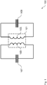
- Fig. 1 shows a diagram of a resonator circuit 100 according to an embodiment.
- the resonator circuit 100 comprises a transformer 101 comprising a primary winding 103 and a secondary winding 105, wherein the primary winding 103 is inductively coupled with the secondary winding 105, a primary capacitor 107 being connected to the primary winding 103, the primary capacitor 107 and the primary winding 103 forming a primary circuit, and a secondary capacitor 109 being connected to the secondary winding 105, the secondary capacitor 109 and the secondary winding 105 forming a secondary circuit, wherein the resonator circuit 100 has a common mode resonance frequency at an excitation of the primary circuit in a common mode, wherein the resonator circuit 100 has a differential mode resonance frequency at an excitation of the primary circuit in a differential mode, and wherein the common mode resonance frequency is different from the differential mode resonance frequency.
- the common mode resonance frequency is twice the differential mode resonance frequency.
- the resonator circuit 100 can be a tank circuit.
- the resonator circuit 100 can be used as a frequency selective element within a radio frequency oscillator.
- the resonator circuit 100 can be resonant when excited in the differential mode and in the common mode.
- the primary winding 103 and the secondary winding 105 can be arranged to provide a strong inductive coupling when the primary circuit is excited in the differential mode and a weak inductive coupling when the primary circuit is excited in the common mode.
- the resonance frequency in differential mode i.e. the differential mode resonance frequency
- the resonance frequency in common mode can depend on the inductance of the primary winding 103, the capacitance of the primary capacitor 107, the inductance of the secondary winding 105, and the capacitance of the secondary capacitor 109.
- the resonance frequency in common mode i.e. the common mode resonance frequency
- the resonance frequency in common mode may be independent from the inductance of the secondary winding 105, and the capacitance of the secondary capacitor 109.
- the diagram illustrates the overall structure of the resonator circuit 100, wherein the primary capacitor 107 can comprise a pair of single-ended capacitors, and wherein the secondary capacitor 109 can comprise a pair of differential capacitors.
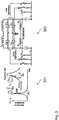
- Fig. 2 shows a diagram of a radio frequency oscillator 200 according to an embodiment.
- the radio frequency oscillator 200 comprises a resonator circuit 100, and an excitation circuit 201.
- the resonator circuit 100 comprises a transformer 101 comprising a primary winding 103 and a secondary winding 105, wherein the primary winding 103 is inductively coupled with the secondary winding 105, a primary capacitor 107 being connected to the primary winding 103, the primary capacitor 107 and the primary winding 103 forming a primary circuit, and a secondary capacitor 109 being connected to the secondary winding 105, the secondary capacitor 109 and the secondary winding 105 forming a secondary circuit, wherein the resonator circuit 100 has a common mode resonance frequency at an excitation of the primary circuit in a common mode, wherein the resonator circuit 100 has a differential mode resonance frequency at an excitation of the primary circuit in a differential mode, and wherein the common mode resonance frequency is different from the differential mode resonance frequency.
- the excitation circuit 201 comprises at least one transisbr, in particular at least one field-effect transistor, for exciting the primary circuit of the resonator circuit 100.
- at least two transistors may be employed.
- An up-conversion of flicker noise can degrade a close-in spectrum of a radio frequency oscillator, e.g. a complementary metal-oxide semiconductor (CMOS) radio frequency (RF) oscillator.
- CMOS complementary metal-oxide semiconductor
- RF radio frequency
- the resulting 1/f 3 phase noise (PN) can further be an issue within phase-locked loops (PLLs) having a loop bandwidth of e.g. less than 1 MHz, which practically relates to the majority of cellular phones.
- PLLs phase-locked loops
- a major flicker noise up-conversion mechanism in nanoscale CMOS is the Groszkowski effect.
- the presence of harmonics in a current of an active device can cause a frequency drift of a resonance frequency of a resonator circuit, due to perturbing reactive energy in the resonator circuit.
- Any variation in a higher to fundamental current harmonics ratio e.g. due to the flicker noise can modulate the frequency drift and can show itself as a 1/f 3 phase noise.
- Embodiments of the invention reduce the flicker noise up-conversion due to the Groszkowski effect in radio frequency oscillators significantly.
- the resonator circuit 100 can be applied for flicker noise up-conversion reduction within the radio frequency oscillator 200, wherein the radio frequency oscillator 200 can be a class F oscillator.
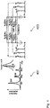
- Fig. 3 shows an input impedance response 301 and an equivalent circuit 303 of a resonator circuit.
- the diagram illustrates current harmonic paths and frequency drifts for the resonator circuit without resistive traps at higher harmonics.
- harmonics of a current of an active device can cause a frequency drift of a resonance frequency ⁇ 0 of a resonator circuit as depicted in Fig. 3 .
- a fundamental drain current I H1 can flow into the resistors having the resistance R p , which can be the equivalent parallel resistance of the resonator circuit, while its second and third harmonics, I H2 and I H3 , may mainly take the capacitance path due to its lower impedance.
- reactive energy stored in the inductors and capacitors e.g.
- Fig. 4 shows an input impedance response 401 and an equivalent circuit 403 of a resonator circuit 100 according to an embodiment.
- the diagram illustrates current harmonic paths and frequency drifts for the resonator circuit 100 with resistive traps at higher harmonics.
- the input impedance Z in of the resonator circuit 100 has further peaks at strong harmonics of the fundamental resonance frequency ⁇ 0 . These harmonics would then mainly flow into their relative equivalent resistance of Z in , instead of its capacitive part, as depicted in Fig. 4 . Consequently, Groszewski's effect on the flicker noise up-conversion can be reduced significantly.
- flicker noise of transistors, e.g. core transistors, of an excitation circuit can modulate the second harmonic of the virtual ground of the radio frequency oscillator. This modulation can generate a second harmonic current in parasitic gate-source capacitors C gs and can get injected into the resonator circuit 100. Consequently, the current I H2 can be the main contributor to the frequency drift.
- a dominant source of 1/f noise up-conversion in radio frequency oscillators is that current harmonics of the resonator circuits flow into the capacitive part of the resonator circuits as shown in Fig. 3 .
- An approach for reducing the 1/f noise up-conversion is illustrated in Fig. 4 .
- the current can flow into the equivalent resistance of the resonator circuit and 1/f noise up-conversion can be reduced.
- a resonator circuit 100 is generally shown in Fig. 1 .
- Embodiments of the invention apply a transformer-based resonator circuit topology that effectively traps the current I H2 in its resistive part without the cost of extra die area on a semiconductor substrate.
- the resonator circuit 100 can derive this characteristic from a different behavior of inductors and transformers in differential mode (DM) and common mode (CM) excitations.
- the transformer based resonator circuit 100 can be incorporated into the radio frequency oscillator 200, e.g. a class-F oscillator, in order to take advantage of its low phase noise in the 20dB/dec region and in order to improve the phase noise in the 30dB/dec region.
- the resonator circuit 100 can be based on the transformer 101, e.g. being a 1:2 turn transformer.
- the differential mode resonance frequency and the common mode resonance frequency can be different within the transformer 101, e.g. due to different coupling factors in differential mode and in common mode. An application of a switch is avoided.
- the resistive trap is realized by the common mode resonance.
- the common mode signal that excites the common mode resonance can be the second harmonic component of the current within the resonator circuit 100.
- the I H2 component can have a ⁇ /2 phase shift with regard to the fundamental current which can make it a common mode signal as illustrated in Fig. 3 and Fig. 4 .
- the common mode resonance frequency can be two times the differential mode resonance frequency. Then, the common mode second harmonic current component can flow into the equivalent resistance of the resonant peak and may not flow through the capacitive part. This approach mitigates disturbances of the reactive energy in the capacitive part and reduces the 1/f noise up-conversion.
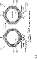
- Fig. 5 shows a transformer 101 comprising a primary winding 103 and a secondary winding 105 according to an embodiment.
- the diagram illustrates the currents within the primary winding 103 and the secondary winding 105 when the transformer 101 is excited in differential mode (DM) and in common mode (CM).
- the transformer 101 can be an F 2,3 transformer.
- the primary winding 103 of the transformer 101 and the secondary winding 105 of the transformer 101 are planar and are arranged on the same plane.
- the secondary winding 105 of the transformer 101 comprises a bridging portion being arranged at a different plane.
- the primary winding 103 of the transformer 101 and the secondary winding 105 of the transformer 101 are connected to a supply voltage or an AC ground potential.
- the connection is realized by a symmetrical center tapping of the primary winding 103 and the secondary winding 105.
- the transformer 101 having a 1:2 turn ratio, can be excited by differential mode and common mode input signals at its primary winding 103.
- differential mode excitation the induced currents at the secondary winding 105 can circulate in the same directions leading to a strong coupling factor k m .
- common mode excitation the induced currents can cancel each other, resulting in a weak coupling factor k m .
- the inductance of the primary winding 103 can be referred to as L p
- the inductance of the secondary winding 105 can be referred to as L s
- the capacitance of the primary capacitor 107 can be referred to as C p
- the capacitance of the secondary capacitor 109 can be referred to as C s .
- the primary winding 103, the secondary winding 105, the primary capacitor 107, and the secondary capacitor 109 are considered as individual concentrated components.
- the inductance of the primary winding 103 can be referred to as 2 L p
- the inductance of the secondary winding 105 can be referred to as 2 L s
- the capacitance of the primary capacitor 107 can be referred to as 0.5 C p
- the capacitance of the secondary capacitor 109 can be referred to as 0.5 C s
- the primary winding 103 and the secondary winding 105 are each formed by a pair of inductors connected in series, wherein the inductance of each inductor is referred to as L p or L s , respectively.
- the primary capacitor 107 and the secondary capacitor 109 are each formed by a pair of capacitors connected in series, wherein the capacitance of each capacitor is referred to as C p or C s , respectively.
- L pd can relate to half of the inductance of the primary winding 103 in differential mode, e.g. the inductance between a center tap of the primary winding 103 and one of the inputs, yielding a total differential primary capacitance of 2 L p .
- the inductance associated with the primary winding 103 in differential mode and the inductance associated with the primary winding 103 in common mode are considered to be equal.
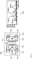
- Fig. 6 shows a resonator circuit 100 and an input impedance response 609 according to an embodiment.
- the resonator circuit 100 comprises a transformer 101 comprising a primary winding 103 and a secondary winding 105, wherein the primary winding 103 is inductively coupled with the secondary winding 105, a primary capacitor 107 being connected to the primary winding 103, the primary capacitor 107 and the primary winding 103 forming a primary circuit, and a secondary capacitor 109 being connected to the secondary winding 105, the secondary capacitor 109 and the secondary winding 105 forming a secondary circuit, wherein the resonator circuit 100 has a common mode resonance frequency at an excitation of the primary circuit in a common mode, wherein the resonator circuit 100 has a differential mode resonance frequency at an excitation of the primary circuit in a differential mode, and wherein the common mode resonance frequency is different from the differential mode resonance frequency.
- Fig. 6 shows a possible realization of the resonator circuit 100.
- the primary capacitor 107 of the primary circuit comprises a pair of single-ended capacitors 601, 603.
- the secondary capacitor 109 of the secondary circuit comprises a pair of differential capacitors 605, 607.
- the primary capacitor 107 and the secondary capacitor 109 are variable capacitors, in particular digitally tunable capacitors.
- the pair of single-ended capacitors 601, 603 and the pair of differential capacitors 605, 607 are variable capacitors, in particular digitally tunable capacitors.
- the differential mode resonance frequency and/or the common mode resonance frequency are tunable between a minimum frequency f min and a maximum frequency f max , respectively, as illustrated by the input impedance response 609.
- the input impedance of the resonator circuit 100 is denoted as Z in .
- the resonator circuit 100 can employ the transformer 101, the pair of single-ended capacitors 601, 603 within the primary circuit and the pair of differential capacitors 605, 607 within the secondary circuit.
- the resonator circuit 100 can be an F 2,3 resonator circuit.
- the transformer 101 can be an F 2,3 transformer.
- the resonator circuit 100 can have two differential mode resonance frequencies and one common mode resonance frequency.
- the inductance associated with the primary winding 103 in common mode L pc can be greater than the inductance associated with the primary winding 103 in differential mode L pd , i.e. L pc > L pd , due to a metal track inductance L T connecting e.g. a center tap of the primary winding 103 to a constant supply voltage.
- a lower coupling factor k m may be used in order to satisfy both F 2 and F 3 operation conditions of the resonator circuit 100.
- a careful design of the single-ended capacitors 601, 603 within the primary circuit and/or the differential capacitors 605, 607 within the secondary circuit, which can be variable capacitors, can maintain ⁇ CM / ⁇ 0,DM ⁇ 2 and ⁇ 1.DM / ⁇ 0,DM ⁇ 3 over the full tuning range (TR).
- Fig. 7 shows a diagram of a radio frequency oscillator 200 according to an embodiment.
- the radio frequency oscillator 200 comprises a resonator drcuit 100, and an excitation circuit 201.
- the resonator circuit 100 forms an implementation of the resonator circuit 100 as described in conjunction with Fig. 6 .
- the excitation circuit 201 comprises a transistor 701, a transistor 703, a tail resistor 705, and a tail capacitor 707.
- the radio frequency oscillator 200 is a class F oscillator.
- the specific impulse sensitivity function (ISF) of the pseudo square-wave oscillation waveform can lead to an improved phase noise performance.
- the current I H2 can be as high as the current I H3 .
- a class F 3 resonator circuit is replaced by a class F 2,3 resonator circuit.
- the pseudo square-wave oscillation waveform of class F oscillators can be preserved, wherein a 1/f 3 phase noise corner frequency can be reduced e.g.
- Embodiments of the invention use an F 2,3 resonator circuit and the different characteristics of a 1:2 turn transformer in differential mode and common mode excitations in order to provide a resistive trap at the second harmonic 2 ⁇ 0 , resulting in a reduction of flicker noise up-conversion in radio frequency oscillators.
- Fig. 8 shows a diagram of a single-ended capacitor 601, 603 according to an embodiment.
- the single-ended capacitor 601, 603 comprises a capacitor 801, a capacitor 803, a transistor 805, a transistor 807, a resistor 809, a resistor 811, an inverter 813, and an inverter 815.
- the single-ended capacitor 601, 603 is arranged within the primary circuit.
- the transistor 805 and the transistor 807 can be switched between a conducting state and a non-conducting state. Consequently, the capacitance of the single-ended capacitor 601, 603 can be digitally tuned.
- a plurality of single-ended capacitors 601, 603 can be connected in parallel.
- Fig. 9 shows a diagram of a differential capacitor 605, 607 according to an embodiment.
- the differential capacitor 605, 607 comprises a capacitor 901, a capacitor 903, a transistor 905, a resistor 907, a resistor 909, an inverter 911, and an inverter 913.
- the differential capacitor 605, 607 is arranged within the secondary circuit.
- the transistor 905 By applying a digital switching signal b i , the transistor 905 can be switched between a conducting state and a non-conducting state. Consequently, the capacitance of the differential capacitor 605, 607 can be digitally tuned. A plurality of differential capacitors 605, 607 can be connected in parallel.
- Fig. 10 shows a diagram of a tail resistor 705 of a radio frequency oscillator 200 according to an embodiment.
- the tail resistor 705 comprises a transistor 1001, and a resistor 1003.
- the tail resistor 705 can be used for current control within the radio frequency oscillator 200.
- the transistor 1001 By applying a digital switching signal b i , the transistor 1001 can be switched between a conducting state and a non-conducting state. Consequently, the current within the radio frequency oscillator 200 can be controlled.
- a plurality of tail resistors 705 can be connected in parallel and/or in series.
- Fig. 11 shows a phase noise power spectral density 1101 of a radio frequency oscillator 200 according to an embodiment.
- the diagram depicts the phase noise power spectral density in dBc/Hz over a carrier frequency offset in Hz.
- the radio frequency oscillator 200 is a class F 2,3 oscillator.
- the diagram relates to a minimum frequency of 5.4 GHz and a maximum frequency of 7 GHz.
- a 1/f 3 phase noise corner is further depicted in the diagram.
Landscapes
- Engineering & Computer Science (AREA)
- Power Engineering (AREA)
- Computer Networks & Wireless Communication (AREA)
- Signal Processing (AREA)
- Inductance-Capacitance Distribution Constants And Capacitance-Resistance Oscillators (AREA)
- Filters And Equalizers (AREA)
Description
- The invention relates to the field of radio frequency (RF) resonator circuits.
- Resonator circuits, also denoted as tank circuits, are widely used as frequency selective elements in a variety of radio frequency components, such as filters, amplifiers, and oscillators. Typically, resonator circuits comprise inductors and capacitors, wherein the inductors and capacitors are connected to be in resonance at a specific resonance frequency. The quality of resonator circuits is thereby characterized by a quality factor. The characteristics of resonator circuits are of major interest in the design of radio frequency oscillators, in particular when implemented as radio frequency integrated circuits (RFICs) on semiconductor substrates. In particular, the response of the resonator circuits with regard to leakage currents or currents at harmonic frequencies can have a major impact on the frequency stability and phase noise performance of the radio frequency oscillators.
- Common resonator circuits exhibit a resistive characteristic when excited at the resonance frequency, and a capacitive characteristic when excited at frequencies above the resonance frequency. Consequently, higher order current components in conjunction with the Groszkowski effect may lead to reduced frequency stability and increased flicker noise up-conversion, i.e. reduced close-in phase noise performance, of radio frequency oscillators.
- For improving the phase noise performance of radio frequency oscillators, noise filtering techniques are applied. These techniques rely on interposing a further resonator circuit having a resonance frequency at 2ω0 in a common source of the transistors, e.g. core transistors. These techniques, however, use an additional tunable inductor and increase the die area on the semiconductor substrate.
- For reducing an amount of higher order drain current harmonics, resistors are added in series with the sources of the transistors for linearizing the operation of the transistors. However, the radio frequency oscillator start-up margin is usually reduced.
- By adding resistors in series with the drain of the transistors, the resistance in conjunction with a parasitic drain capacitance can introduce a delay in a loop gain for shifting both an impulse sensitivity function (ISF) and a current waveform of the radio frequency oscillators. Flicker noise up-conversion is reduced by specifically tailoring the component values. However, the phase noise performance in the 20dB/decade region is degraded particularly at low supply voltages and high current consumptions.
- In J. Groszkowski, "The interdependence of frequency variation and harmonic content, and the problem of constant-frequency oscillators," Proc. IRE, vol. 21, no. 7, pp. 958-981, Jul. 1934, the Groszkowski effect is studied.
- In M. Babaie and R. B. Staszewski, "A class-F CMOS oscillator," IEEE JSSC, vol. 48, no.12, pp. 3120-3133, Dec. 2013, a resonator circuit and a radio frequency oscillator are described.
-
US 2012/0161890 A1 describes a VCO including an LC resonator having an even and odd resonant mode. - The document "Transformer-Based Dual-Mode Voltage-Controlled Oscillators", IEEE TRANSACTIONS ON CIRCUITS AND SYSTEMS II: ANALOG AND DIGITALSIGNAL PROCESSING, INSTITUTE OF ELECTRICAL AND ELECTRONICS ENGINEERS INC, 345 EAST 47 STREET, NEW YORK, N.Y. 10017, USA, vol. 54, no. 4, pages 293-297, XP011176988 describes a dual-mode oscillator built using a transformer-based resonator.
-
US 2011/018644 A1 relates to an oscillator connected to a resonance unit suited to oscillate frequencies in multiple bands. - DONGHYUN BAEK ET AL: "A dual-band (13/22-GHz) VCO based on resonant mode switching", IEEE MICROWAVE AND WIRELESS COMPONENTS LETTERS, IEEE SERVICE CENTER, NEW YORK, NY, US, vol. 13, no. 10, pages 443-445, XP011427858, relates to a dual band voltage controlled oscillator that can cover two bands.
-
US 2014/077890 A1 and the document "A Class-F CMOS Oscillator", IEEE Journal of Solid-State Circuits, vol. 48, no. 12, pages 3120-3133, XP055214112 disclose an oscillator exploiting the time-variant phase noise model, - The document "Third-harmonic injection technique applied to a 5.87-to-7.56GHz 65nm CMOS Class-F oscillator with 192dBc/Hz FOM", SOLID-STATE CIRCUITS CONFERENCE DIGEST OF TECHNICAL PAPERS, pages 348-349, XP032350601, describes an oscillator with a resonator including a transformer and tuning capacitors.
- It is an object of the invention to provide an efficient resonator circuit.
- This object is achieved by the features of
independent claim 1. Further implementation forms are apparent from the dependent claims, the description and the figures. - The invention is based on the finding that a transformer-based resonator circuit can be employed exhibiting different characteristics when excited in a differential mode and in a common mode. In particular, the inductive coupling factor of the transformer may be different in differential mode and common mode excitations, wherein a differential mode resonance frequency can be different from a common mode resonance frequency. In particular, the common mode resonance frequency can be designed to be twice the differential mode resonance frequency.
- The resonator circuit enables an efficient operation of a radio frequency oscillator. In particular, a second harmonic can be exposed to a resistive path provided by the resonator circuit. Consequently, the Groszkowski effect can be mitigated and frequency stability and phase noise performance of the radio frequency oscillator can be improved.
- The resonator circuit and the radio frequency oscillator are suited for implementation as radio frequency integrated circuits (RFICs) on semiconductor substrates.
- According to a first aspect, the invention relates to a resonator circuit, the resonator circuit comprising a transformer comprising a primary winding and a secondary winding, wherein the primary winding is inductively coupled with the secondary winding, a primary capacitor being connected to the primary winding, the primary capacitor and the primary winding forming a primary circuit, and a secondary capacitor being connected to the secondary winding, the secondary capacitor and the secondary winding forming a secondary circuit, wherein the resonator circuit has a common mode resonance frequency at an excitation of the primary circuit in a common mode, wherein the resonator circuit has a differential mode resonance frequency at an excitation of the primary circuit in a differential mode, wherein the common mode resonance frequency is different from the differential mode resonance frequency, and wherein a ratio of turns of the primary winding and the secondary winding is 1:2, with the primary winding of the transformer or the secondary winding of the transformer being planar and arranged on the same plane, wherein the common mode resonance frequency is twice the differential mode resonance frequency. Thus, an efficient resonator circuit is provided.
- The resonator circuit can be a tank circuit. The resonator circuit can be used as a frequency selective element within a radio frequency oscillator. The resonator circuit can be resonant when excited in the differential mode and in the common mode.
- The primary winding and the secondary winding can be arranged to provide a strong inductive coupling when the primary circuit is excited in the differential mode and a weak inductive coupling when the primary circuit is excited in the common mode.
- The primary capacitor can comprise a pair of single-ended capacitors being connected in series to form the primary capacitor. The primary capacitor can be regarded as a primary capacitive structure. The secondary capacitor can comprise a pair of differential capacitors being connected in series to form the secondary capacitor. The secondary capacitor can be regarded as a secondary capacitive structure.
- The resonance frequency in differential mode, i.e. the differential mode resonance frequency, can depend on the inductance of the primary winding, the capacitance of the primary capacitor, the inductance of the secondary winding, and the capacitance of the secondary capacitor. The resonance frequency in common mode, i.e. the common mode resonance frequency, can depend on the inductance of the primary winding and the capacitance of the primary capacitor. The resonance frequency in common mode, i.e. the common mode resonance frequency, may be independent from the inductance of the secondary winding, and the capacitance of the secondary capacitor. Odd order harmonic components of the current injected into the resonator circuit can be differential mode signals and even order harmonic components can be common mode signals.
- In a first implementation form of the resonator circuit according to the first aspect as such, the common mode resonance frequency is twice the differential mode resonance frequency. Thus, a resistive path for a second harmonic at an excitation of the primary circuit in the common mode is realized.
- In a second implementation form of the resonator circuit according to the first aspect as such or any preceding implementation form of the first aspect, the resonator circuit has a further differential mode resonance frequency at an excitation of the primary circuit in the differential mode, wherein the further differential mode resonance frequency is different from the differential mode resonance frequency and the common mode resonance frequency. Thus, a further differential mode resonance at the further differential mode resonance frequency is realized.
- In a third implementation form of the resonator circuit according to the second implementation form of the first aspect, the further differential mode resonance frequency is three times the differential mode resonance frequency. Thus, a resistive path for a third harmonic at an excitation of the primary circuit in the differential mode is realized. The further differential mode resonance frequency can specifically be designed to be three times the differential mode resonance frequency.
- In a fourth implementation form of the resonator circuit according to the first aspect as such or any preceding implementation form of the first aspect, the primary winding of the transformer comprises one turn, and the secondary winding of the transformer comprises two turns. Thus, the resonator circuit is implemented efficiently.
- The primary winding of the transformer and/or the secondary winding of the transformer can comprise a bridging portion being arranged at a different plane.
- In a fifth implementation form of the resonator circuit according to the first aspect as such or any preceding implementation form of the first aspect, the primary winding of the transformer and/or the secondary winding of the transformer is connected to a constant voltage source or a ground potential. Thus, a tapping of the primary winding and/or the secondary winding is realized. Both the primary winding and the secondary winding may be connected to a constant voltage source respectively in order to enable an efficient start-up of the resonator circuit.
- The tapping of the primary winding and/or the secondary winding can be a symmetrical center tapping of the primary winding and/or the secondary winding.
- In a sixth implementation form of the resonator circuit according to the first aspect as such or any preceding implementation form of the first aspect, the primary capacitor of the primary circuit comprises a pair of single-ended capacitors. Thus, a reference to ground potential of the primary circuit is realized. The pair of single-ended capacitors can have the same capacitance as the primary capacitor. A single-ended capacitor can be realized as a plurality of switched capacitors, wherein the plurality of switched capacitors can be arranged in parallel. The capacitances of the switched capacitors can be different.
- In a seventh implementation form of the resonator circuit according to the first aspect as such or any preceding implementation form of the first aspect, the secondary capacitor of the secondary circuit comprises a pair of differential capacitors. Thus, a reference to ground potential of the secondary circuit is avoided. A differential capacitor can be realized as a plurality of switched capacitors, wherein the plurality of switched capacitors can be arranged in parallel. The pair of differential capacitors can be a pair of balanced capacitors.
- In an eighth implementation form of the resonator circuit according to the first aspect as such or any preceding implementation form of the first aspect, the primary capacitor and/or the secondary capacitor comprises a variable capacitor, in particular a digitally tunable capacitor. Thus, a variation of the differential mode resonance frequency and/or the common mode resonance frequency can be realized efficiently.
- In a ninth implementation form of the resonator circuit according to the first aspect as such or any preceding implementation form of the first aspect, the primary capacitor is connected in parallel to the primary winding, and/or the secondary capacitor is connected in parallel to the secondary winding. Thus, the resonator circuit is implemented efficiently. According to a second aspect, the invention relates to a radio frequency oscillator, the radio frequency oscillator comprising a resonator circuit according to the first aspect as such or any implementation form of the first aspect, and an excitation circuit being configured to excite the primary circuit of the resonator circuit in the differential mode. Thus, an efficient radio frequency oscillator is provided.
- The radio frequency oscillator can exhibit improved frequency stability and phase noise performance, e.g. close-in phase noise performance. In particular, flicker noise up-conversion due to the Groszkowski effect can be mitigated efficiently. The approach may be effective to mitigate a 1/f phase noise up-conversion and may therefore improve a 1/f3 phase noise characteristic. A 1/f2 phase noise characteristic may be unchanged.
- Further features of the radio frequency oscillator directly result from the functionality of the resonator circuit according to the first aspect as such or any implementation form of the first aspect.
- In a first implementation form of the radio frequency oscillator according to the second aspect as such, the excitation circuit comprises at least one transistor, in particular at least one field-effect transistor, for exciting the primary circuit of the resonator circuit. Thus, an active device is employed for exciting the primary circuit of the resonator circuit. In order to realize a cross-coupled oscillator structure at least two transistors may be employed. The transistors can be metal-oxide-semiconductor field-effect transistors (MOSFETs).
- In a second implementation form of the radio frequency oscillator according to the second aspect as such or any preceding implementation form of the second aspect, the radio frequency oscillator is a class F oscillator. Thus, an efficient oscillator structure is applied.
- Within the class F oscillator, a first harmonic and a third harmonic can be excited in order to obtain a pseudo square-wave oscillation waveform. Within the class F oscillator, the third harmonic may not be filtered due to the further differential mode resonance frequency. The oscillation signal can have a pseudo square-wave oscillation waveform.
- The invention can be implemented using hardware and/or software.
- Embodiments of the invention will be described with respect to the following figures, in which:
- Fig. 1
- shows a diagram of a resonator circuit according to an embodiment;
- Fig. 2
- shows a diagram of a radio frequency oscillator according to an embodiment;
- Fig. 3
- shows an input impedance response and an equivalent circuit of a resonator circuit;
- Fig. 4
- shows an input impedance response and an equivalent circuit of a resonator circuit according to an embodiment;
- Fig. 5
- shows a transformer comprising a primary winding and a secondary winding according to an embodiment;
- Fig. 6
- shows a resonator circuit and an input impedance response according to an embodiment;
- Fig. 7
- shows a diagram of a radio frequency oscillator according to an embodiment;
- Fig. 8
- shows a diagram of a single-ended capacitor according to an embodiment;
- Fig. 9
- shows a diagram of a differential capacitor according to an embodiment;
- Fig. 10
- shows a diagram of a tail resistor of a radio frequency oscillator according to an embodiment; and
- Fig. 11
- shows a phase noise power spectral density of a radio frequency oscillator according to an embodiment.
-
Fig. 1 shows a diagram of aresonator circuit 100 according to an embodiment. Theresonator circuit 100 comprises atransformer 101 comprising a primary winding 103 and a secondary winding 105, wherein the primary winding 103 is inductively coupled with the secondary winding 105, aprimary capacitor 107 being connected to the primary winding 103, theprimary capacitor 107 and the primary winding 103 forming a primary circuit, and asecondary capacitor 109 being connected to the secondary winding 105, thesecondary capacitor 109 and the secondary winding 105 forming a secondary circuit, wherein theresonator circuit 100 has a common mode resonance frequency at an excitation of the primary circuit in a common mode, wherein theresonator circuit 100 has a differential mode resonance frequency at an excitation of the primary circuit in a differential mode, and wherein the common mode resonance frequency is different from the differential mode resonance frequency. In an embodiment, the common mode resonance frequency is twice the differential mode resonance frequency. - The
resonator circuit 100 can be a tank circuit. Theresonator circuit 100 can be used as a frequency selective element within a radio frequency oscillator. Theresonator circuit 100 can be resonant when excited in the differential mode and in the common mode. - The primary winding 103 and the secondary winding 105 can be arranged to provide a strong inductive coupling when the primary circuit is excited in the differential mode and a weak inductive coupling when the primary circuit is excited in the common mode.
- The resonance frequency in differential mode, i.e. the differential mode resonance frequency, can depend on the inductance of the primary winding 103, the capacitance of the
primary capacitor 107, the inductance of the secondary winding 105, and the capacitance of thesecondary capacitor 109. The resonance frequency in common mode, i.e. the common mode resonance frequency, can depend on the inductance of the primary winding 103 and the capacitance of theprimary capacitor 107. The resonance frequency in common mode, i.e. the common mode resonance frequency, may be independent from the inductance of the secondary winding 105, and the capacitance of thesecondary capacitor 109. - The diagram illustrates the overall structure of the
resonator circuit 100, wherein theprimary capacitor 107 can comprise a pair of single-ended capacitors, and wherein thesecondary capacitor 109 can comprise a pair of differential capacitors. -
Fig. 2 shows a diagram of aradio frequency oscillator 200 according to an embodiment. Theradio frequency oscillator 200 comprises aresonator circuit 100, and anexcitation circuit 201. Theresonator circuit 100 comprises atransformer 101 comprising a primary winding 103 and a secondary winding 105, wherein the primary winding 103 is inductively coupled with the secondary winding 105, aprimary capacitor 107 being connected to the primary winding 103, theprimary capacitor 107 and the primary winding 103 forming a primary circuit, and asecondary capacitor 109 being connected to the secondary winding 105, thesecondary capacitor 109 and the secondary winding 105 forming a secondary circuit, wherein theresonator circuit 100 has a common mode resonance frequency at an excitation of the primary circuit in a common mode, wherein theresonator circuit 100 has a differential mode resonance frequency at an excitation of the primary circuit in a differential mode, and wherein the common mode resonance frequency is different from the differential mode resonance frequency. Theexcitation circuit 201 is configured to excite the primary circuit of theresonator circuit 100 in the differential mode. Theexcitation circuit 201 can exemplarily comprise an exciting element, e.g. a feedback amplifier, providing a trans-conductance Gm. - In an embodiment, the
excitation circuit 201 comprises at least one transisbr, in particular at least one field-effect transistor, for exciting the primary circuit of theresonator circuit 100. In order to realize a cross-coupled oscillator structure at least two transistors may be employed. - In the following, further implementation forms and embodiments of the
resonator circuit 100 and the radio frequency oscillator200 are described. - An up-conversion of flicker noise, e.g. 1/f noise, can degrade a close-in spectrum of a radio frequency oscillator, e.g. a complementary metal-oxide semiconductor (CMOS) radio frequency (RF) oscillator. The resulting 1/f3 phase noise (PN) can further be an issue within phase-locked loops (PLLs) having a loop bandwidth of e.g. less than 1 MHz, which practically relates to the majority of cellular phones. A major flicker noise up-conversion mechanism in nanoscale CMOS is the Groszkowski effect.
- The presence of harmonics in a current of an active device, such as a transistor of an excitation circuit, can cause a frequency drift of a resonance frequency of a resonator circuit, due to perturbing reactive energy in the resonator circuit. Any variation in a higher to fundamental current harmonics ratio e.g. due to the flicker noise can modulate the frequency drift and can show itself as a 1/f3 phase noise. Embodiments of the invention reduce the flicker noise up-conversion due to the Groszkowski effect in radio frequency oscillators significantly. The
resonator circuit 100 can be applied for flicker noise up-conversion reduction within theradio frequency oscillator 200, wherein theradio frequency oscillator 200 can be a class F oscillator. -
Fig. 3 shows aninput impedance response 301 and anequivalent circuit 303 of a resonator circuit. The diagram illustrates current harmonic paths and frequency drifts for the resonator circuit without resistive traps at higher harmonics. - The presence of harmonics of a current of an active device, such as a transistor of an excitation circuit, can cause a frequency drift of a resonance frequency ω0 of a resonator circuit as depicted in
Fig. 3 . A fundamental drain current IH1 can flow into the resistors having the resistance Rp, which can be the equivalent parallel resistance of the resonator circuit, while its second and third harmonics, IH2 and IH3, may mainly take the capacitance path due to its lower impedance. As a consequence, reactive energy stored in the inductors and capacitors, e.g. having inductances Lp and capacitances Cc and Cd, can be perturbed, shifting the resonance frequency ω0 and/or the oscillation frequency by Δω lower in order to satisfy the resonance condition. This shift may be static but any variation in the ratio of the currents IH2 (or IH3) to IH1 e.g. due to flicker noise can modulate Δω and can show itself as a 1/f3 phase noise. -
Fig. 4 shows aninput impedance response 401 and anequivalent circuit 403 of aresonator circuit 100 according to an embodiment. The diagram illustrates current harmonic paths and frequency drifts for theresonator circuit 100 with resistive traps at higher harmonics. - Suppose that the input impedance Zin of the
resonator circuit 100 has further peaks at strong harmonics of the fundamental resonance frequency ω0. These harmonics would then mainly flow into their relative equivalent resistance of Zin, instead of its capacitive part, as depicted inFig. 4 . Consequently, Groszewski's effect on the flicker noise up-conversion can be reduced significantly. On the other hand, flicker noise of transistors, e.g. core transistors, of an excitation circuit can modulate the second harmonic of the virtual ground of the radio frequency oscillator. This modulation can generate a second harmonic current in parasitic gate-source capacitors Cgs and can get injected into theresonator circuit 100. Consequently, the current IH2 can be the main contributor to the frequency drift. - In other words, a dominant source of 1/f noise up-conversion in radio frequency oscillators, in particular without tail transistors, is that current harmonics of the resonator circuits flow into the capacitive part of the resonator circuits as shown in
Fig. 3 . An approach for reducing the 1/f noise up-conversion is illustrated inFig. 4 . For resonance frequencies at higher harmonics, the current can flow into the equivalent resistance of the resonator circuit and 1/f noise up-conversion can be reduced. Aresonator circuit 100 is generally shown inFig. 1 . - Embodiments of the invention apply a transformer-based resonator circuit topology that effectively traps the current IH2 in its resistive part without the cost of extra die area on a semiconductor substrate. The
resonator circuit 100 can derive this characteristic from a different behavior of inductors and transformers in differential mode (DM) and common mode (CM) excitations. The transformer basedresonator circuit 100 can be incorporated into theradio frequency oscillator 200, e.g. a class-F oscillator, in order to take advantage of its low phase noise in the 20dB/dec region and in order to improve the phase noise in the 30dB/dec region. - The
resonator circuit 100 can be based on thetransformer 101, e.g. being a 1:2 turn transformer. The differential mode resonance frequency and the common mode resonance frequency can be different within thetransformer 101, e.g. due to different coupling factors in differential mode and in common mode. An application of a switch is avoided. The resistive trap is realized by the common mode resonance. - The common mode signal that excites the common mode resonance can be the second harmonic component of the current within the
resonator circuit 100. The IH2 component can have a π/2 phase shift with regard to the fundamental current which can make it a common mode signal as illustrated inFig. 3 andFig. 4 . - If the space of the primary winding and/or the secondary winding is designed accurately and a ratio Cs/Cp is chosen accurately, the common mode resonance frequency can be two times the differential mode resonance frequency. Then, the common mode second harmonic current component can flow into the equivalent resistance of the resonant peak and may not flow through the capacitive part. This approach mitigates disturbances of the reactive energy in the capacitive part and reduces the 1/f noise up-conversion.
-
Fig. 5 shows atransformer 101 comprising a primary winding 103 and a secondary winding 105 according to an embodiment. The diagram illustrates the currents within the primary winding 103 and the secondary winding 105 when thetransformer 101 is excited in differential mode (DM) and in common mode (CM). Thetransformer 101 can be an F2,3 transformer. - The primary winding 103 of the
transformer 101 and the secondary winding 105 of thetransformer 101 are planar and are arranged on the same plane. The secondary winding 105 of thetransformer 101 comprises a bridging portion being arranged at a different plane. - The primary winding 103 of the
transformer 101 and the secondary winding 105 of thetransformer 101 are connected to a supply voltage or an AC ground potential. The connection is realized by a symmetrical center tapping of the primary winding 103 and the secondary winding 105. - The
transformer 101, having a 1:2 turn ratio, can be excited by differential mode and common mode input signals at its primary winding 103. In differential mode excitation, the induced currents at the secondary winding 105 can circulate in the same directions leading to a strong coupling factor km. On the other hand, in common mode excitation, the induced currents can cancel each other, resulting in a weak coupling factor km. - The inductance of the primary winding 103 can be referred to as Lp, the inductance of the secondary winding 105 can be referred to as Ls, the capacitance of the
primary capacitor 107 can be referred to as Cp, and the capacitance of thesecondary capacitor 109 can be referred to as Cs. According to this definition, the primary winding 103, the secondary winding 105, theprimary capacitor 107, and thesecondary capacitor 109 are considered as individual concentrated components. - Alternatively, the inductance of the primary winding 103 can be referred to as 2 Lp, the inductance of the secondary winding 105 can be referred to as 2 Ls, the capacitance of the
primary capacitor 107 can be referred to as 0.5 Cp, and the capacitance of thesecondary capacitor 109 can be referred to as 0.5 Cs. According to this definition, the primary winding 103 and the secondary winding 105 are each formed by a pair of inductors connected in series, wherein the inductance of each inductor is referred to as Lp or Ls, respectively. Furthermore, theprimary capacitor 107 and thesecondary capacitor 109 are each formed by a pair of capacitors connected in series, wherein the capacitance of each capacitor is referred to as Cp or Cs, respectively. - The differential mode resonance frequency can be determined according to the following equation:

primary capacitor 107, Ls denotes an inductance associated with the secondary winding 105, and Cs denotes a capacitance associated with asecondary capacitor 109. - The common mode resonance frequency can be determined according to the following equation:

primary capacitor 107. - Lpd can relate to half of the inductance of the primary winding 103 in differential mode, e.g. the inductance between a center tap of the primary winding 103 and one of the inputs, yielding a total differential primary capacitance of 2 Lp. This is due to the consideration that the inductance LT may not be seen in differential excitation but may affect the inductance in common mode excitation. The total inductance in common mode excitation can be equal to 2 Lpd + 2 LT, or Lpc = Lpd + LT as used in the equations.
- In an embodiment, the inductance associated with the primary winding 103 in differential mode and the inductance associated with the primary winding 103 in common mode are considered to be equal.
-
Fig. 6 shows aresonator circuit 100 and aninput impedance response 609 according to an embodiment. Theresonator circuit 100 comprises atransformer 101 comprising a primary winding 103 and a secondary winding 105, wherein the primary winding 103 is inductively coupled with the secondary winding 105, aprimary capacitor 107 being connected to the primary winding 103, theprimary capacitor 107 and the primary winding 103 forming a primary circuit, and asecondary capacitor 109 being connected to the secondary winding 105, thesecondary capacitor 109 and the secondary winding 105 forming a secondary circuit, wherein theresonator circuit 100 has a common mode resonance frequency at an excitation of the primary circuit in a common mode, wherein theresonator circuit 100 has a differential mode resonance frequency at an excitation of the primary circuit in a differential mode, and wherein the common mode resonance frequency is different from the differential mode resonance frequency.Fig. 6 shows a possible realization of theresonator circuit 100. - The
primary capacitor 107 of the primary circuit comprises a pair of single-endedcapacitors secondary capacitor 109 of the secondary circuit comprises a pair ofdifferential capacitors primary capacitor 107 and thesecondary capacitor 109 are variable capacitors, in particular digitally tunable capacitors. In particular, the pair of single-endedcapacitors differential capacitors input impedance response 609. The input impedance of theresonator circuit 100 is denoted as Zin. - The
resonator circuit 100 can employ thetransformer 101, the pair of single-endedcapacitors differential capacitors resonator circuit 100 can be an F2,3 resonator circuit. Thetransformer 101 can be an F2,3 transformer. Theresonator circuit 100 can have two differential mode resonance frequencies and one common mode resonance frequency. - For class-F3 operation, ω1,DM = 3ω0,DM, and for resistive traps at the second and third harmonics, ωCM = 2ω0,DM and ω1,DM=3ω0,DM. This can result in LsCs = 3LpCp and km = 0.72, wherein km denotes the coupling factor between the primary winding 103 and the secondary winding 105.
- When implementing the
resonator circuit 100, the inductance associated with the primary winding 103 in common mode Lpc can be greater than the inductance associated with the primary winding 103 in differential mode Lpd, i.e. Lpc > Lpd, due to a metal track inductance LT connecting e.g. a center tap of the primary winding 103 to a constant supply voltage. Thus, a lower coupling factor km may be used in order to satisfy both F2 and F3 operation conditions of theresonator circuit 100. A careful design of the single-endedcapacitors differential capacitors - In an embodiment, the inductance associated with the primary winding 103 in common mode Lpc is determined according to the following equation:

-
Fig. 7 shows a diagram of aradio frequency oscillator 200 according to an embodiment. Theradio frequency oscillator 200 comprises aresonator drcuit 100, and anexcitation circuit 201. Theresonator circuit 100 forms an implementation of theresonator circuit 100 as described in conjunction withFig. 6 . Theexcitation circuit 201 comprises atransistor 701, atransistor 703, atail resistor 705, and atail capacitor 707. Theradio frequency oscillator 200 is a class F oscillator. - Class F3 oscillators can have a pseudo square-wave oscillation waveform by designing ω1,DM = 3ω0,DM, and avoiding filtering the current IH3 in a resonator circuit. The specific impulse sensitivity function (ISF) of the pseudo square-wave oscillation waveform can lead to an improved phase noise performance. In this oscillator, the current IH2 can be as high as the current IH3. In a class F2,3 oscillator, a class F3 resonator circuit is replaced by a class F2,3 resonator circuit. The pseudo square-wave oscillation waveform of class F oscillators can be preserved, wherein a 1/f3 phase noise corner frequency can be reduced e.g. from 300 kHz to 700 kHz to less than 30 kHz. Embodiments of the invention use an F2,3 resonator circuit and the different characteristics of a 1:2 turn transformer in differential mode and common mode excitations in order to provide a resistive trap at the second harmonic 2ω0, resulting in a reduction of flicker noise up-conversion in radio frequency oscillators.
-
Fig. 8 shows a diagram of a single-endedcapacitor capacitor capacitor 801, acapacitor 803, atransistor 805, atransistor 807, aresistor 809, aresistor 811, aninverter 813, and aninverter 815. The single-endedcapacitor - By applying a digital switching signal bi, the
transistor 805 and thetransistor 807 can be switched between a conducting state and a non-conducting state. Consequently, the capacitance of the single-endedcapacitor capacitors -
Fig. 9 shows a diagram of adifferential capacitor differential capacitor capacitor 901, acapacitor 903, atransistor 905, aresistor 907, aresistor 909, aninverter 911, and aninverter 913. Thedifferential capacitor - By applying a digital switching signal bi, the
transistor 905 can be switched between a conducting state and a non-conducting state. Consequently, the capacitance of thedifferential capacitor differential capacitors -
Fig. 10 shows a diagram of atail resistor 705 of aradio frequency oscillator 200 according to an embodiment. Thetail resistor 705 comprises atransistor 1001, and aresistor 1003. Thetail resistor 705 can be used for current control within theradio frequency oscillator 200. - By applying a digital switching signal bi, the
transistor 1001 can be switched between a conducting state and a non-conducting state. Consequently, the current within theradio frequency oscillator 200 can be controlled. A plurality oftail resistors 705 can be connected in parallel and/or in series. -
Fig. 11 shows a phase noise powerspectral density 1101 of aradio frequency oscillator 200 according to an embodiment. The diagram depicts the phase noise power spectral density in dBc/Hz over a carrier frequency offset in Hz. Theradio frequency oscillator 200 is a class F2,3 oscillator. - The diagram relates to a minimum frequency of 5.4 GHz and a maximum frequency of 7 GHz. A 1/f3 phase noise corner is further depicted in the diagram.
Claims (12)
- A resonator circuit (100), comprising:a transformer (101) comprising a primary winding (103) and a secondary winding (105), wherein the primary winding (103) is inductively coupled with the secondary winding (105);a primary capacitor (107) being connected to the primary winding (103), the primary capacitor (107) and the primary winding (103) forming a primary circuit; anda secondary capacitor (109) being connected to the secondary winding (105), the secondary capacitor (109) and the secondary winding (105) forming a secondary circuit;wherein the resonator circuit (100) has a common mode resonance frequency at an excitation of the primary circuit in a common mode, wherein the resonator circuit (100) has a differential mode resonance frequency at an excitation of the primary circuit in a differential mode, and wherein the common mode resonance frequency is different from the differential mode resonance frequency,characterized in thata ratio of turns of the primary winding and the secondary winding is 1:2, with the primary winding (103) of the transformer (101) or the secondary winding (105) of the transformer (101) being planar and arranged on the same plane, wherein the common mode resonance frequency is twice the differential mode resonance frequency.
- The resonator circuit (100) of any of the preceding claims, wherein the resonator circuit (100) has a further differential mode resonance frequency at an excitation of the primary circuit in the differential mode, wherein the further differential mode resonance frequency is different from the differential mode resonance frequency and the common mode resonance frequency.
- The resonator circuit (100) of claim 2, wherein the further differential mode resonance frequency is three times the differential mode resonance frequency.
- The resonator circuit (100) of any of the preceding claims, wherein the primary winding (103) of the transformer (101) comprises one turn, and wherein the secondary winding (105) of the transformer (101) comprises two turns.
- The resonator circuit (100) of any of the preceding claims, wherein the primary winding (103) of the transformer (101) or the secondary winding (105) of the transformer (101) is connected to a constant voltage source or a ground potential.
- The resonator circuit (100) of any of the preceding claims, wherein the primary capacitor (107) of the primary circuit comprises a pair of single-ended capacitors (601, 603).
- The resonator circuit (100) of any of the preceding claims, wherein the secondary capacitor (109) of the secondary circuit comprises a pair of differential capacitors (605, 607).
- The resonator circuit (100) of any of the preceding claims, wherein the primary capacitor (107) or the secondary capacitor (109) comprises a variable capacitor, in particular a digitally tunable capacitor.
- The resonator circuit (100) of any of the preceding claims, wherein the primary capacitor (107) is connected in parallel to the primary winding (103), or wherein the secondary capacitor (109) is connected in parallel to the secondary winding (105).
- A radio frequency oscillator (200), comprising:a resonator circuit (100) according to any of the claims 1 to 9; andan excitation circuit (201) being configured to excite the primary circuit of the resonator circuit (100) in the differential mode.
- The radio frequency oscillator (200) of claim 10, wherein the excitation circuit (201) comprises at least one transistor (701, 703), in particular at least one field-effect transistor, for exciting the primary circuit of the resonator circuit (100).
- The radio frequency oscillator (200) of claims 10 or 11, wherein the radio frequency oscillator (200) is a class F oscillator.
Priority Applications (1)
| Application Number | Priority Date | Filing Date | Title |
|---|---|---|---|
| EP21176396.6A EP3952106A3 (en) | 2015-01-27 | 2015-01-27 | A resonator circuit |
Applications Claiming Priority (1)
| Application Number | Priority Date | Filing Date | Title |
|---|---|---|---|
| PCT/EP2015/051573 WO2016119823A1 (en) | 2015-01-27 | 2015-01-27 | A resonator circuit |
Related Child Applications (1)
| Application Number | Title | Priority Date | Filing Date |
|---|---|---|---|
| EP21176396.6A Division EP3952106A3 (en) | 2015-01-27 | 2015-01-27 | A resonator circuit |
Publications (2)
| Publication Number | Publication Date |
|---|---|
| EP3158641A1 EP3158641A1 (en) | 2017-04-26 |
| EP3158641B1 true EP3158641B1 (en) | 2021-06-16 |
Family
ID=52432809
Family Applications (2)
| Application Number | Title | Priority Date | Filing Date |
|---|---|---|---|
| EP15701524.9A Active EP3158641B1 (en) | 2015-01-27 | 2015-01-27 | A resonator circuit |
| EP21176396.6A Pending EP3952106A3 (en) | 2015-01-27 | 2015-01-27 | A resonator circuit |
Family Applications After (1)
| Application Number | Title | Priority Date | Filing Date |
|---|---|---|---|
| EP21176396.6A Pending EP3952106A3 (en) | 2015-01-27 | 2015-01-27 | A resonator circuit |
Country Status (4)
| Country | Link |
|---|---|
| US (4) | US10637395B2 (en) |
| EP (2) | EP3158641B1 (en) |
| CN (3) | CN111510070A (en) |
| WO (1) | WO2016119823A1 (en) |
Families Citing this family (10)
| Publication number | Priority date | Publication date | Assignee | Title |
|---|---|---|---|---|
| CN111510070A (en) * | 2015-01-27 | 2020-08-07 | 华为技术有限公司 | resonator circuit |
| WO2016119824A1 (en) | 2015-01-27 | 2016-08-04 | Huawei Technologies Co., Ltd. | A radio frequency oscillator |
| WO2018023367A1 (en) * | 2016-08-02 | 2018-02-08 | 华为技术有限公司 | Voltage waveform shaping oscillator |
| EP3504790A1 (en) * | 2016-08-23 | 2019-07-03 | Telefonaktiebolaget LM Ericsson (publ) | Biasing circuit for capacitor switch transistor and method therefore |
| CN111756329A (en) * | 2016-11-04 | 2020-10-09 | 华为技术有限公司 | Dual Mode Oscillators and Multiphase Oscillators |
| CN107731480B (en) * | 2017-08-21 | 2020-10-30 | 武汉船用电力推进装置研究所(中国船舶重工集团公司第七一二研究所) | High leakage inductance differential mode reactor for power electronic converter |
| US10652050B2 (en) * | 2018-05-01 | 2020-05-12 | Linear Technology Holding Llc | Power over data lines system using split or coupled CMCs and DMCs for coupling DC voltage and attenuating common mode noise |
| CN111277228B (en) * | 2018-12-04 | 2023-04-07 | 炬芯科技股份有限公司 | Radio frequency transceiver, storage medium and even harmonic suppression method of power amplifier |
| US10778145B2 (en) * | 2019-01-02 | 2020-09-15 | Mediatek Inc. | Magnetically pumped voltage controlled oscillator |
| CN111147021B (en) * | 2020-04-03 | 2020-07-24 | 恒玄科技(上海)股份有限公司 | Voltage controlled oscillator |
Citations (2)
| Publication number | Priority date | Publication date | Assignee | Title |
|---|---|---|---|---|
| US6606008B2 (en) * | 2000-11-17 | 2003-08-12 | Infineon Technologies Ag | Oscillator circuit |
| US20130309983A1 (en) * | 2011-12-19 | 2013-11-21 | Ori Ashckenazi | Voltage-controlled oscillator with reduced single-ended capacitance |
Family Cites Families (22)
| Publication number | Priority date | Publication date | Assignee | Title |
|---|---|---|---|---|
| US7091813B2 (en) * | 2002-06-13 | 2006-08-15 | International Business Machines Corporation | Integrated circuit transformer for radio frequency applications |
| US7158049B2 (en) | 2003-03-24 | 2007-01-02 | Schlumberger Technology Corporation | Wireless communication circuit |
| US7116183B2 (en) * | 2004-02-05 | 2006-10-03 | Qualcomm Incorporated | Temperature compensated voltage controlled oscillator |
| JP2005303839A (en) * | 2004-04-14 | 2005-10-27 | Matsushita Electric Ind Co Ltd | Voltage controlled oscillator |
| US7154349B2 (en) * | 2004-08-11 | 2006-12-26 | Qualcomm, Incorporated | Coupled-inductor multi-band VCO |
| US7764127B2 (en) * | 2006-11-30 | 2010-07-27 | Qualcomm, Incorporated | High resolution digitally controlled oscillator |
| US7683733B2 (en) * | 2008-02-04 | 2010-03-23 | Freescale Semiconductor, Inc. | Balun transformer with improved harmonic suppression |
| US7936224B2 (en) * | 2008-04-22 | 2011-05-03 | Mediatek Inc. | Voltage controlled oscillator |
| US8736392B2 (en) * | 2009-03-18 | 2014-05-27 | Qualcomm Incorporated | Transformer-based CMOS oscillators |
| US8264293B2 (en) * | 2009-07-27 | 2012-09-11 | Electronics And Telecommunications Research Institute | Oscillator |
| SG10201508705VA (en) * | 2010-10-21 | 2015-11-27 | Univ Nanyang Tech | Integrated Circuit Architecture With Strongly Coupled LC Tanks |
| US8294528B2 (en) * | 2010-12-28 | 2012-10-23 | Qualcomm Incorporated | Wideband multi-mode VCO |
| CN102255502B (en) * | 2011-07-16 | 2014-04-16 | 西安电子科技大学 | Primary inductance correction circuit applied to flyback switching power supply |
| WO2013091708A1 (en) * | 2011-12-22 | 2013-06-27 | Huawei Technologies Co., Ltd. | Oscillator circuit and method for generating an oscillation |
| US9118335B2 (en) * | 2012-09-16 | 2015-08-25 | Technische Universiteit Delft | High resolution millimeter wave digitally controlled oscillator with reconfigurable distributed metal capacitor passive resonators |
| US9330832B2 (en) * | 2013-02-13 | 2016-05-03 | Nokia Technologies Oy | Integrated transformer balun with enhanced common-mode rejection for radio frequency, microwave, and millimeter-wave integrated circuits |
| US9077310B2 (en) * | 2013-05-30 | 2015-07-07 | Mediatek Inc. | Radio frequency transmitter, power combiners and terminations therefor |
| CN103762859A (en) * | 2014-02-26 | 2014-04-30 | 杨华新 | Non-electrolytic isolated type syntonic switching power supply |
| US9667193B2 (en) * | 2014-07-30 | 2017-05-30 | Texas Instruments Incorporated | Low power wide tuning range oscillator |
| WO2016054612A1 (en) * | 2014-10-03 | 2016-04-07 | Zaretsky, Howard | Switching current source radio frequency oscillator |
| WO2016119824A1 (en) * | 2015-01-27 | 2016-08-04 | Huawei Technologies Co., Ltd. | A radio frequency oscillator |
| CN111510070A (en) * | 2015-01-27 | 2020-08-07 | 华为技术有限公司 | resonator circuit |
-
2015
- 2015-01-27 CN CN202010279868.5A patent/CN111510070A/en active Pending
- 2015-01-27 EP EP15701524.9A patent/EP3158641B1/en active Active
- 2015-01-27 WO PCT/EP2015/051573 patent/WO2016119823A1/en not_active Ceased
- 2015-01-27 EP EP21176396.6A patent/EP3952106A3/en active Pending
- 2015-01-27 CN CN202010279883.XA patent/CN111510071B/en active Active
- 2015-01-27 CN CN201580044943.7A patent/CN106664059B/en active Active
-
2017
- 2017-07-25 US US15/659,204 patent/US10637395B2/en active Active
-
2020
- 2020-03-27 US US16/833,182 patent/US11025197B2/en active Active
-
2021
- 2021-04-20 US US17/235,474 patent/US11323069B2/en active Active
-
2022
- 2022-04-01 US US17/711,825 patent/US11646697B2/en active Active
Patent Citations (2)
| Publication number | Priority date | Publication date | Assignee | Title |
|---|---|---|---|---|
| US6606008B2 (en) * | 2000-11-17 | 2003-08-12 | Infineon Technologies Ag | Oscillator circuit |
| US20130309983A1 (en) * | 2011-12-19 | 2013-11-21 | Ori Ashckenazi | Voltage-controlled oscillator with reduced single-ended capacitance |
Also Published As
| Publication number | Publication date |
|---|---|
| US20220294393A1 (en) | 2022-09-15 |
| CN111510070A (en) | 2020-08-07 |
| CN111510071B (en) | 2023-12-08 |
| US11646697B2 (en) | 2023-05-09 |
| CN111510071A (en) | 2020-08-07 |
| CN106664059A (en) | 2017-05-10 |
| CN106664059B (en) | 2020-04-28 |
| EP3952106A2 (en) | 2022-02-09 |
| EP3158641A1 (en) | 2017-04-26 |
| US20170366137A1 (en) | 2017-12-21 |
| US11025197B2 (en) | 2021-06-01 |
| US10637395B2 (en) | 2020-04-28 |
| US20200304068A1 (en) | 2020-09-24 |
| EP3952106A3 (en) | 2022-05-04 |
| WO2016119823A1 (en) | 2016-08-04 |
| US11323069B2 (en) | 2022-05-03 |
| US20210313931A1 (en) | 2021-10-07 |
Similar Documents
| Publication | Publication Date | Title |
|---|---|---|
| US11646697B2 (en) | Resonator circuit | |
| US11770101B2 (en) | Radio frequency oscillator | |
| US9337847B2 (en) | Oscillator | |
| US20140077890A1 (en) | Class-f cmos oscillator | |
| US20090289727A1 (en) | Oscillator for generating different oscillations | |
| US20090289732A1 (en) | Semiconductor integrated circuit device and frequency synthesizer | |
| US20110074513A1 (en) | Dual-Band Voltage-Controlled Oscillator Arrangement | |
| US7286024B2 (en) | Voltage-controlled oscillator with differential output | |
| Khan et al. | Low power LC-quadrature VCO with superior phase noise performance in 0.13 µm RF-CMOS process for modern WLAN application | |
| US9099957B2 (en) | Voltage-controlled oscillators and related systems | |
| US9698727B1 (en) | Coupled inductor-based resonator | |
| US9106179B2 (en) | Voltage-controlled oscillators and related systems | |
| Azizi Poor et al. | A low phase noise quadrature VCO using superharmonic injection, current reuse, and negative resistance techniques in CMOS technology | |
| Wu et al. | A 12.5–50 GHz frequency synthesizer for Software-Defined Radios in 40-nm CMOS |
Legal Events
| Date | Code | Title | Description |
|---|---|---|---|
| STAA | Information on the status of an ep patent application or granted ep patent |
Free format text: STATUS: THE INTERNATIONAL PUBLICATION HAS BEEN MADE |
|
| PUAI | Public reference made under article 153(3) epc to a published international application that has entered the european phase |
Free format text: ORIGINAL CODE: 0009012 |
|
| STAA | Information on the status of an ep patent application or granted ep patent |
Free format text: STATUS: REQUEST FOR EXAMINATION WAS MADE |
|
| 17P | Request for examination filed |
Effective date: 20170123 |
|
| AK | Designated contracting states |
Kind code of ref document: A1 Designated state(s): AL AT BE BG CH CY CZ DE DK EE ES FI FR GB GR HR HU IE IS IT LI LT LU LV MC MK MT NL NO PL PT RO RS SE SI SK SM TR |
|
| AX | Request for extension of the european patent |
Extension state: BA ME |
|
| DAX | Request for extension of the european patent (deleted) | ||
| STAA | Information on the status of an ep patent application or granted ep patent |
Free format text: STATUS: EXAMINATION IS IN PROGRESS |
|
| 17Q | First examination report despatched |
Effective date: 20200102 |
|
| RAP1 | Party data changed (applicant data changed or rights of an application transferred) |
Owner name: HUAWEI TECHNOLOGIES CO., LTD. |
|
| GRAP | Despatch of communication of intention to grant a patent |
Free format text: ORIGINAL CODE: EPIDOSNIGR1 |
|
| STAA | Information on the status of an ep patent application or granted ep patent |
Free format text: STATUS: GRANT OF PATENT IS INTENDED |
|
| INTG | Intention to grant announced |
Effective date: 20201222 |
|
| GRAS | Grant fee paid |
Free format text: ORIGINAL CODE: EPIDOSNIGR3 |
|
| GRAA | (expected) grant |
Free format text: ORIGINAL CODE: 0009210 |
|
| STAA | Information on the status of an ep patent application or granted ep patent |
Free format text: STATUS: THE PATENT HAS BEEN GRANTED |
|
| AK | Designated contracting states |
Kind code of ref document: B1 Designated state(s): AL AT BE BG CH CY CZ DE DK EE ES FI FR GB GR HR HU IE IS IT LI LT LU LV MC MK MT NL NO PL PT RO RS SE SI SK SM TR |
|
| REG | Reference to a national code |
Ref country code: GB Ref legal event code: FG4D |
|
| REG | Reference to a national code |
Ref country code: CH Ref legal event code: EP |
|
| REG | Reference to a national code |
Ref country code: DE Ref legal event code: R096 Ref document number: 602015070402 Country of ref document: DE |
|
| REG | Reference to a national code |
Ref country code: AT Ref legal event code: REF Ref document number: 1403178 Country of ref document: AT Kind code of ref document: T Effective date: 20210715 |
|
| REG | Reference to a national code |
Ref country code: IE Ref legal event code: FG4D |
|
| REG | Reference to a national code |
Ref country code: LT Ref legal event code: MG9D |
|
| PG25 | Lapsed in a contracting state [announced via postgrant information from national office to epo] |
Ref country code: FI Free format text: LAPSE BECAUSE OF FAILURE TO SUBMIT A TRANSLATION OF THE DESCRIPTION OR TO PAY THE FEE WITHIN THE PRESCRIBED TIME-LIMIT Effective date: 20210616 Ref country code: LT Free format text: LAPSE BECAUSE OF FAILURE TO SUBMIT A TRANSLATION OF THE DESCRIPTION OR TO PAY THE FEE WITHIN THE PRESCRIBED TIME-LIMIT Effective date: 20210616 Ref country code: HR Free format text: LAPSE BECAUSE OF FAILURE TO SUBMIT A TRANSLATION OF THE DESCRIPTION OR TO PAY THE FEE WITHIN THE PRESCRIBED TIME-LIMIT Effective date: 20210616 Ref country code: BG Free format text: LAPSE BECAUSE OF FAILURE TO SUBMIT A TRANSLATION OF THE DESCRIPTION OR TO PAY THE FEE WITHIN THE PRESCRIBED TIME-LIMIT Effective date: 20210916 |
|
| REG | Reference to a national code |
Ref country code: AT Ref legal event code: MK05 Ref document number: 1403178 Country of ref document: AT Kind code of ref document: T Effective date: 20210616 |
|
| REG | Reference to a national code |
Ref country code: NL Ref legal event code: MP Effective date: 20210616 |
|
| PG25 | Lapsed in a contracting state [announced via postgrant information from national office to epo] |
Ref country code: GR Free format text: LAPSE BECAUSE OF FAILURE TO SUBMIT A TRANSLATION OF THE DESCRIPTION OR TO PAY THE FEE WITHIN THE PRESCRIBED TIME-LIMIT Effective date: 20210917 Ref country code: LV Free format text: LAPSE BECAUSE OF FAILURE TO SUBMIT A TRANSLATION OF THE DESCRIPTION OR TO PAY THE FEE WITHIN THE PRESCRIBED TIME-LIMIT Effective date: 20210616 Ref country code: NO Free format text: LAPSE BECAUSE OF FAILURE TO SUBMIT A TRANSLATION OF THE DESCRIPTION OR TO PAY THE FEE WITHIN THE PRESCRIBED TIME-LIMIT Effective date: 20210916 Ref country code: RS Free format text: LAPSE BECAUSE OF FAILURE TO SUBMIT A TRANSLATION OF THE DESCRIPTION OR TO PAY THE FEE WITHIN THE PRESCRIBED TIME-LIMIT Effective date: 20210616 Ref country code: SE Free format text: LAPSE BECAUSE OF FAILURE TO SUBMIT A TRANSLATION OF THE DESCRIPTION OR TO PAY THE FEE WITHIN THE PRESCRIBED TIME-LIMIT Effective date: 20210616 |
|
| PG25 | Lapsed in a contracting state [announced via postgrant information from national office to epo] |
Ref country code: SM Free format text: LAPSE BECAUSE OF FAILURE TO SUBMIT A TRANSLATION OF THE DESCRIPTION OR TO PAY THE FEE WITHIN THE PRESCRIBED TIME-LIMIT Effective date: 20210616 Ref country code: SK Free format text: LAPSE BECAUSE OF FAILURE TO SUBMIT A TRANSLATION OF THE DESCRIPTION OR TO PAY THE FEE WITHIN THE PRESCRIBED TIME-LIMIT Effective date: 20210616 Ref country code: CZ Free format text: LAPSE BECAUSE OF FAILURE TO SUBMIT A TRANSLATION OF THE DESCRIPTION OR TO PAY THE FEE WITHIN THE PRESCRIBED TIME-LIMIT Effective date: 20210616 Ref country code: EE Free format text: LAPSE BECAUSE OF FAILURE TO SUBMIT A TRANSLATION OF THE DESCRIPTION OR TO PAY THE FEE WITHIN THE PRESCRIBED TIME-LIMIT Effective date: 20210616 Ref country code: NL Free format text: LAPSE BECAUSE OF FAILURE TO SUBMIT A TRANSLATION OF THE DESCRIPTION OR TO PAY THE FEE WITHIN THE PRESCRIBED TIME-LIMIT Effective date: 20210616 Ref country code: PT Free format text: LAPSE BECAUSE OF FAILURE TO SUBMIT A TRANSLATION OF THE DESCRIPTION OR TO PAY THE FEE WITHIN THE PRESCRIBED TIME-LIMIT Effective date: 20211018 Ref country code: RO Free format text: LAPSE BECAUSE OF FAILURE TO SUBMIT A TRANSLATION OF THE DESCRIPTION OR TO PAY THE FEE WITHIN THE PRESCRIBED TIME-LIMIT Effective date: 20210616 Ref country code: ES Free format text: LAPSE BECAUSE OF FAILURE TO SUBMIT A TRANSLATION OF THE DESCRIPTION OR TO PAY THE FEE WITHIN THE PRESCRIBED TIME-LIMIT Effective date: 20210616 Ref country code: AT Free format text: LAPSE BECAUSE OF FAILURE TO SUBMIT A TRANSLATION OF THE DESCRIPTION OR TO PAY THE FEE WITHIN THE PRESCRIBED TIME-LIMIT Effective date: 20210616 |
|
| PG25 | Lapsed in a contracting state [announced via postgrant information from national office to epo] |
Ref country code: PL Free format text: LAPSE BECAUSE OF FAILURE TO SUBMIT A TRANSLATION OF THE DESCRIPTION OR TO PAY THE FEE WITHIN THE PRESCRIBED TIME-LIMIT Effective date: 20210616 |
|
| REG | Reference to a national code |
Ref country code: DE Ref legal event code: R097 Ref document number: 602015070402 Country of ref document: DE |
|
| PLBE | No opposition filed within time limit |
Free format text: ORIGINAL CODE: 0009261 |
|
| STAA | Information on the status of an ep patent application or granted ep patent |
Free format text: STATUS: NO OPPOSITION FILED WITHIN TIME LIMIT |
|
| PG25 | Lapsed in a contracting state [announced via postgrant information from national office to epo] |
Ref country code: DK Free format text: LAPSE BECAUSE OF FAILURE TO SUBMIT A TRANSLATION OF THE DESCRIPTION OR TO PAY THE FEE WITHIN THE PRESCRIBED TIME-LIMIT Effective date: 20210616 |
|
| 26N | No opposition filed |
Effective date: 20220317 |
|
| PG25 | Lapsed in a contracting state [announced via postgrant information from national office to epo] |
Ref country code: AL Free format text: LAPSE BECAUSE OF FAILURE TO SUBMIT A TRANSLATION OF THE DESCRIPTION OR TO PAY THE FEE WITHIN THE PRESCRIBED TIME-LIMIT Effective date: 20210616 |
|
| PG25 | Lapsed in a contracting state [announced via postgrant information from national office to epo] |
Ref country code: IT Free format text: LAPSE BECAUSE OF FAILURE TO SUBMIT A TRANSLATION OF THE DESCRIPTION OR TO PAY THE FEE WITHIN THE PRESCRIBED TIME-LIMIT Effective date: 20210616 |
|
| REG | Reference to a national code |
Ref country code: DE Ref legal event code: R119 Ref document number: 602015070402 Country of ref document: DE |
|
| PG25 | Lapsed in a contracting state [announced via postgrant information from national office to epo] |
Ref country code: MC Free format text: LAPSE BECAUSE OF FAILURE TO SUBMIT A TRANSLATION OF THE DESCRIPTION OR TO PAY THE FEE WITHIN THE PRESCRIBED TIME-LIMIT Effective date: 20210616 |
|
| REG | Reference to a national code |
Ref country code: CH Ref legal event code: PL |
|
| REG | Reference to a national code |
Ref country code: BE Ref legal event code: MM Effective date: 20220131 |
|
| PG25 | Lapsed in a contracting state [announced via postgrant information from national office to epo] |
Ref country code: LU Free format text: LAPSE BECAUSE OF NON-PAYMENT OF DUE FEES Effective date: 20220127 Ref country code: DE Free format text: LAPSE BECAUSE OF NON-PAYMENT OF DUE FEES Effective date: 20220802 |
|
| PG25 | Lapsed in a contracting state [announced via postgrant information from national office to epo] |
Ref country code: FR Free format text: LAPSE BECAUSE OF NON-PAYMENT OF DUE FEES Effective date: 20220131 Ref country code: BE Free format text: LAPSE BECAUSE OF NON-PAYMENT OF DUE FEES Effective date: 20220131 |
|
| PG25 | Lapsed in a contracting state [announced via postgrant information from national office to epo] |
Ref country code: LI Free format text: LAPSE BECAUSE OF NON-PAYMENT OF DUE FEES Effective date: 20220131 Ref country code: CH Free format text: LAPSE BECAUSE OF NON-PAYMENT OF DUE FEES Effective date: 20220131 |
|
| PG25 | Lapsed in a contracting state [announced via postgrant information from national office to epo] |
Ref country code: IE Free format text: LAPSE BECAUSE OF NON-PAYMENT OF DUE FEES Effective date: 20220127 |
|
| P01 | Opt-out of the competence of the unified patent court (upc) registered |
Effective date: 20230524 |
|
| PG25 | Lapsed in a contracting state [announced via postgrant information from national office to epo] |
Ref country code: HU Free format text: LAPSE BECAUSE OF FAILURE TO SUBMIT A TRANSLATION OF THE DESCRIPTION OR TO PAY THE FEE WITHIN THE PRESCRIBED TIME-LIMIT; INVALID AB INITIO Effective date: 20150127 |
|
| PG25 | Lapsed in a contracting state [announced via postgrant information from national office to epo] |
Ref country code: MK Free format text: LAPSE BECAUSE OF FAILURE TO SUBMIT A TRANSLATION OF THE DESCRIPTION OR TO PAY THE FEE WITHIN THE PRESCRIBED TIME-LIMIT Effective date: 20210616 Ref country code: CY Free format text: LAPSE BECAUSE OF FAILURE TO SUBMIT A TRANSLATION OF THE DESCRIPTION OR TO PAY THE FEE WITHIN THE PRESCRIBED TIME-LIMIT Effective date: 20210616 |
|
| PG25 | Lapsed in a contracting state [announced via postgrant information from national office to epo] |
Ref country code: TR Free format text: LAPSE BECAUSE OF FAILURE TO SUBMIT A TRANSLATION OF THE DESCRIPTION OR TO PAY THE FEE WITHIN THE PRESCRIBED TIME-LIMIT Effective date: 20210616 |
|
| PG25 | Lapsed in a contracting state [announced via postgrant information from national office to epo] |
Ref country code: MT Free format text: LAPSE BECAUSE OF FAILURE TO SUBMIT A TRANSLATION OF THE DESCRIPTION OR TO PAY THE FEE WITHIN THE PRESCRIBED TIME-LIMIT Effective date: 20210616 |
|
| PGFP | Annual fee paid to national office [announced via postgrant information from national office to epo] |
Ref country code: GB Payment date: 20251204 Year of fee payment: 12 |